US8611113B2 - Fault protection in voltage source converters with redundant switching cells via mechanical switches being closed pyrotechnically - Google Patents
Fault protection in voltage source converters with redundant switching cells via mechanical switches being closed pyrotechnically Download PDFInfo
- Publication number
- US8611113B2 US8611113B2 US13/144,649 US200913144649A US8611113B2 US 8611113 B2 US8611113 B2 US 8611113B2 US 200913144649 A US200913144649 A US 200913144649A US 8611113 B2 US8611113 B2 US 8611113B2
- Authority
- US
- United States
- Prior art keywords
- switching assembly
- converter according
- switching
- mechanical switch
- semiconductor
- Prior art date
- Legal status (The legal status is an assumption and is not a legal conclusion. Google has not performed a legal analysis and makes no representation as to the accuracy of the status listed.)
- Active, expires
Links
Images


Classifications
-
- H—ELECTRICITY
- H02—GENERATION; CONVERSION OR DISTRIBUTION OF ELECTRIC POWER
- H02M—APPARATUS FOR CONVERSION BETWEEN AC AND AC, BETWEEN AC AND DC, OR BETWEEN DC AND DC, AND FOR USE WITH MAINS OR SIMILAR POWER SUPPLY SYSTEMS; CONVERSION OF DC OR AC INPUT POWER INTO SURGE OUTPUT POWER; CONTROL OR REGULATION THEREOF
- H02M1/00—Details of apparatus for conversion
- H02M1/32—Means for protecting converters other than automatic disconnection
-
- H—ELECTRICITY
- H01—ELECTRIC ELEMENTS
- H01H—ELECTRIC SWITCHES; RELAYS; SELECTORS; EMERGENCY PROTECTIVE DEVICES
- H01H39/00—Switching devices actuated by an explosion produced within the device and initiated by an electric current
-
- H—ELECTRICITY
- H01—ELECTRIC ELEMENTS
- H01H—ELECTRIC SWITCHES; RELAYS; SELECTORS; EMERGENCY PROTECTIVE DEVICES
- H01H39/00—Switching devices actuated by an explosion produced within the device and initiated by an electric current
- H01H39/004—Closing switches
-
- H—ELECTRICITY
- H02—GENERATION; CONVERSION OR DISTRIBUTION OF ELECTRIC POWER
- H02M—APPARATUS FOR CONVERSION BETWEEN AC AND AC, BETWEEN AC AND DC, OR BETWEEN DC AND DC, AND FOR USE WITH MAINS OR SIMILAR POWER SUPPLY SYSTEMS; CONVERSION OF DC OR AC INPUT POWER INTO SURGE OUTPUT POWER; CONTROL OR REGULATION THEREOF
- H02M7/00—Conversion of ac power input into dc power output; Conversion of dc power input into ac power output
- H02M7/42—Conversion of dc power input into ac power output without possibility of reversal
- H02M7/44—Conversion of dc power input into ac power output without possibility of reversal by static converters
- H02M7/48—Conversion of dc power input into ac power output without possibility of reversal by static converters using discharge tubes with control electrode or semiconductor devices with control electrode
- H02M7/483—Converters with outputs that each can have more than two voltages levels
- H02M7/4835—Converters with outputs that each can have more than two voltages levels comprising two or more cells, each including a switchable capacitor, the capacitors having a nominal charge voltage which corresponds to a given fraction of the input voltage, and the capacitors being selectively connected in series to determine the instantaneous output voltage
-
- H—ELECTRICITY
- H02—GENERATION; CONVERSION OR DISTRIBUTION OF ELECTRIC POWER
- H02M—APPARATUS FOR CONVERSION BETWEEN AC AND AC, BETWEEN AC AND DC, OR BETWEEN DC AND DC, AND FOR USE WITH MAINS OR SIMILAR POWER SUPPLY SYSTEMS; CONVERSION OF DC OR AC INPUT POWER INTO SURGE OUTPUT POWER; CONTROL OR REGULATION THEREOF
- H02M7/00—Conversion of ac power input into dc power output; Conversion of dc power input into ac power output
- H02M7/66—Conversion of ac power input into dc power output; Conversion of dc power input into ac power output with possibility of reversal
- H02M7/68—Conversion of ac power input into dc power output; Conversion of dc power input into ac power output with possibility of reversal by static converters
- H02M7/72—Conversion of ac power input into dc power output; Conversion of dc power input into ac power output with possibility of reversal by static converters using discharge tubes with control electrode or semiconductor devices with control electrode
- H02M7/79—Conversion of ac power input into dc power output; Conversion of dc power input into ac power output with possibility of reversal by static converters using discharge tubes with control electrode or semiconductor devices with control electrode using devices of a triode or transistor type requiring continuous application of a control signal
- H02M7/797—Conversion of ac power input into dc power output; Conversion of dc power input into ac power output with possibility of reversal by static converters using discharge tubes with control electrode or semiconductor devices with control electrode using devices of a triode or transistor type requiring continuous application of a control signal using semiconductor devices only
-
- H—ELECTRICITY
- H02—GENERATION; CONVERSION OR DISTRIBUTION OF ELECTRIC POWER
- H02M—APPARATUS FOR CONVERSION BETWEEN AC AND AC, BETWEEN AC AND DC, OR BETWEEN DC AND DC, AND FOR USE WITH MAINS OR SIMILAR POWER SUPPLY SYSTEMS; CONVERSION OF DC OR AC INPUT POWER INTO SURGE OUTPUT POWER; CONTROL OR REGULATION THEREOF
- H02M1/00—Details of apparatus for conversion
- H02M1/32—Means for protecting converters other than automatic disconnection
- H02M1/325—Means for protecting converters other than automatic disconnection with means for allowing continuous operation despite a fault, i.e. fault tolerant converters
Definitions
- the present invention relates to a Voltage Source Converter having at least one phase leg connecting to opposite poles of a direct voltage side of the converter and comprising a series connection of switching assemblies, each switching assembly having an electrically conducting plate member carrying a plurality of semiconductor chips each having at least a semiconductor device of turn-off type and a free-wheeling diode connected in parallel therewith said chips being connected in parallel with each other by each being connected by an individual conductor member to a said plate member of an adjacent switching assembly of said series connection of switching assemblies, a midpoint of said series connection forming a phase output being configured to be connected to an alternating voltage side of the converter and to divide the phase leg into an upper valve branch and a lower valve branch.
- Such converters with any number of said phase legs are comprised, but they have normally three such phase legs for having a three phase alternating voltage on the alternating voltage side thereof.
- the present invention is not restricted to any type of Voltage Source Converters, but it comprises for example Voltage Source Converters of the type known through for example DE 101 03 031 A1 and WO 2007/023064 A1, which are normally called multiple-cell converters of M2LCs, as well as two-level converters having current valves controlled for alternatively connecting one of said poles to said phase output and NPC (Neutral Point Clamped) converters.
- a Voltage Source Converter of this type may be used in all kinds of situations, in which direct voltage is to be converted into alternating voltage and conversely, in which examples of such uses are in stations of HVDC-plants (High Voltage Direct Current), in which direct voltage is normally converted into a three-phase alternating voltage or conversely, or in so-called back-to-back-stations in which alternating voltage is firstly converted into direct voltage and this is then converted into alternating voltage, as well as in SVCs (Static Var Compensator), in which the direct voltage side consists of capacitors hanging freely.
- HVDC-plants High Voltage Direct Current
- SVCs Static Var Compensator
- the direct voltage side consists of capacitors hanging freely.
- the present invention is not restricted to these applications, but other applications are also conceivable, such as in different types of drive systems for machines, vehicles etc.
- the present invention is not restricted to any particular voltage levels between said opposite poles of the direct voltage side of the converter, but these levels shall be that high that a comparatively high number of switching assemblies are to be connected in series for making it possible for them to together hold said voltage in a blocking state of said semiconductor devices.
- a switching assembly in such a Voltage Source Converter has a plurality of said semiconductor chips connected in parallel, the IGBTs of which are controlled simultaneously to be in a conducting or a blocking state and to share the current through the switching assembly when they are in a conducting state. Continued operation of the Voltage Source Converter has to be ensured would one IGBT fail. Extra switching assemblies, i.e. more switching assemblies than are needed for holding the voltage to be held thereby for taking the voltage between said two poles, are in a Voltage Source Converter of this type arranged in said series connection of switching assemblies, so that it would not constitute any problem if one of them would stop function as long as this does not stop the current through the converter.
- One type of Voltage Source Converters has said individual conductor members connecting the respective semiconductor chip to a said plate member in the form of bonded wires, and in a case of a short circuit in one IGBT of such a chip all the current through the switching assembly will flow through this chip and the bonded wire connected thereto will burn through and the current will then jump to another semiconductor chip in parallel therewith.
- all the semiconductor chips of the switching assembly have been consumed in this way operation of the Voltage Source Converter has to be stopped and the switching assembly failed has to be replaced.
- the object of the present invention is to provide a Voltage Source Converter of the type defined in the introduction, which is improved in at least some aspect with respect to the ability of handling failures of semiconductor chips thereof compared to such Voltage Source Converters already known.
- This object is according to the invention obtained by providing such a Voltage Source Converter, which is characterized in that
- a Voltage Source Converter of this type may be designed to conduct very high DC-currents, such as in the order of twice as much as otherwise or more, without any necessity of premature operation stops of the converter. More exactly, no thought have to be spent on for how long time a semiconductor device may take a certain short circuit current when the number of the semiconductor devices connected in parallel in each switching assembly is selected, but this number may be determined by solely considering the current to be conducted therethrough during normal operation.
- a plurality of said conductor members of each semiconductor assembly are designed to burn through upon occurrence of a short circuit current through the relevant semiconductor chip while creating an arc
- said fuse member is associated with a plurality of these conductor members designed to burn through.
- said at least one conductor member designed to burn through is a wire, preferably a flexible wire, such as a thin bonded wire.
- a wire preferably a flexible wire, such as a thin bonded wire.
- said release mechanism comprises an explosive medium, such as gun powder, configured to be ignited by said fuse member so as to move said movable contact to a position corresponding to a closed state of the mechanical switch.
- said release mechanism comprises a member storing potential energy and means holding this member under pretention, and said holding means is configured to be released by burning of a said fuse member associated therewith while allowing said potential energy storing member to release potential energy while urging said movable contact to a position corresponding to a closed state of said mechanical switch.
- said potential energy storing member is preferably a spring member, such as a mechanical compression spring.
- each switching assembly comprises at least one energy storing capacitor connected in parallel with said semiconductor chips thereof, and said switching assembly is configured to obtain two switching states by control of said semiconductor devices of each semiconductor chip, namely a first switching state and a second switching state, in which the voltage across said at least one energy storing capacitor and a zero voltage, respectively, is applied across said plate member of said switching assembly and the plate member to which the semiconductor chips belonging to this switching assembly connect, for obtaining a determined alternating voltage on said phase output.
- Such a Voltage Source Converter is particularly interesting when high powers are to be transmitted therethrough, which means that the number of switching assemblies connected in series in said phase leg is comparatively high.
- a high number of such switching assemblies connected in series means that it will be possible to control these switching assemblies to change between said first and second switching state and by that already at said phase output obtain an alternating voltage being very close to a sinusoidal voltage.
- This may be obtained already by means of substantially lower switching frequencies than typically used in known Voltage Source Converters having fewer possible levels, such as only two or three, of the voltage pulses delivered to said phase output of the converter. This makes it possible to obtain substantially lower losses and also considerably reduces problems of filtering and harmonic currents and radio interferences, so that equipment therefore may be less costly.
- the present invention also relates to a converter having switching assemblies belonging to the same said valve branch configured to be controlled simultaneously so as to alternatively connect one of said opposite poles to said phase output, which constitutes another embodiment of the invention.
- said semiconductor devices of the semiconductor chips are IGBTs (Insulated Gate Bipolar Transistor), IGBTs (Integrated Gate Commutated Thyristor) or GTOs (Gate Turn-Off Thyristor), in which the invention is particularly directed to the case of IGBTs.
- IGBTs Insulated Gate Bipolar Transistor
- IGBTs Integrated Gate Commutated Thyristor
- GTOs Gate Turn-Off Thyristor
- said converter is configured to have said direct voltage side connected to a direct voltage network for transmitting High Voltage Direct Current (HVDC) and the alternating voltage side connected to an alternating voltage phase line belonging to an alternating voltage network.
- HVDC High Voltage Direct Current
- the converter is a part of a SVC (Static Var Compensator) with a direct voltage side formed by energy storing capacitors and the alternating voltage phase output connected to an alternating voltage network.
- SVC Static Var Compensator
- the converter is configured to have a direct voltage across said two poles being 1 kV-1200 kV, 10 kV-1200 kV or 100 kV-1200 kV.
- the invention is the more interesting the higher the direct voltage is.
- the converter is configured to conduct a current of 200 A to 10 kA or 1 kA to 7 kA or 2 kA to 5 kA on the direct voltage side thereof.
- a current of 200 A to 10 kA or 1 kA to 7 kA or 2 kA to 5 kA on the direct voltage side thereof.
- currents above 2 kA are mostly in Voltage Source Converters of this type already known not complying with the existing requirements of operation without stops, but these current levels are well possible to allow in a Voltage Source Converter according to the present invention.
- the invention also relates to a plant for transmitting electric power according to the appended claim therefor.
- the stations of such a plant may be given a high reliability to a competitively low cost.
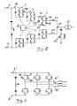
- FIG. 1 is a very simplified view of a Voltage Source Converter of the type according to the present invention
- FIG. 2 is a simplified view very schematically illustrating a Voltage Source Converter of a type to which the present invention may be applied,
- FIG. 3 is a simplified view very schematically illustrating a Voltage Source Converter according to another type to which the present invention may be applied,
- FIG. 4 is a very simplified view illustrating the principle of connecting switching assemblies in series in a Voltage Source Converter
- FIG. 5 is a very simplified view from above of a switching assembly in a Voltage Source Converter
- FIG. 6 is a view corresponding to FIG. 4 of a part of a switching assembly in a Voltage Source Converter according to a first embodiment of the present invention in a state of normal operation of this switching assembly,
- FIG. 7 is a view corresponding to FIG. 6 in a state of bypassing said switching assembly
- FIG. 8 is a view corresponding to FIG. 6 of a switching assembly in a Voltage Source Converter according to a second embodiment of the invention.
- FIG. 1 illustrates very schematically the general construction of a Voltage Source Converter 1 of the type to which the present invention relates.
- This converter has three phase legs 2 - 4 connected to opposite poles 5 , 6 of a direct voltage side of the converter, such as a direct voltage network for transmitting high voltage direct current.
- Each phase leg comprises a series connection of switching assemblies 7 indicated by boxes, in the present case 16 to the number, but this number may be much higher, such as 50, and there are some more than required for holding the voltage they have to hold together between said poles.
- This series connection is divided into two equal parts, an upper valve branch 8 and a lower valve branch 9 , separated by a mid point 10 - 12 forming a phase output being configured to be connected to an alternating voltage side of the converter.
- the phase outputs 10 - 12 may possibly through a transformer connect to a three phase alternating voltage network, load, etc. Filtering equipment is also arranged on said alternating voltage side for improving the shape of the alternating voltage on said alternating voltage side.
- a control arrangement 13 is arranged for controlling the switching assemblies 7 and by that the converter to convert direct voltage into alternating voltage and conversely.
- the Voltage Source Converter has switching assemblies 7 of the type having a plurality of semiconductor chips with each a semiconductor device of turn-off type and a free wheeling diode connected in parallel therewith. These chips are connected in parallel with each other.
- at least one energy storing capacitor is connected in parallel with the semiconductor chips.
- the terminals 14 , 15 of the switching assemblies are adapted to be connected to adjacent switching assemblies in the series connection of switching assemblies forming a phase leg.
- the semiconductor devices 16 , 17 are in this case IGBTs connected in parallel with diodes 18 , 19 .
- An energy storing capacitor 20 is connected in parallel with the respective series connection of the diodes and the semiconductor devices.
- One terminal 14 is connected to the mid point between the two semiconductor devices as well as the mid point between the two diodes.
- the other terminal 15 is connected to the energy storing capacitor 20 .
- the switching assemblies shown in FIG. 2 may be controlled to obtain one of a) a first switching state and b) a second switching state, in which for a) the voltage across the capacitor 20 and for b) a zero voltage is applied across the terminals 14 , 15 .
- FIG. 2 shows the converter according to FIG. 1 , in which totally ten switching assemblies have been left out for simplifying the drawing.
- the control arrangement 13 is adapted to control the switching assemblies by controlling the semiconductor devices thereof, so that they will either deliver a zero voltage or the voltage across the capacitor to be added to the voltages of the other switching assemblies in said series connection.
- a transformer 21 and filtering equipment 22 are here also indicated. It is shown how each valve branch is through a phase reactor 50 , 51 connected to the phase output 10 , and such phase reactors should also be there in FIG. 1 for the phase outputs 10 , 11 and 12 , but have there been left out for simplifying the illustration.
- FIG. 3 schematically illustrates another type of Voltage Source Converter to which the present invention may apply, which is of a so-called two level type and the switching assemblies 7 ′ belonging to the same valve branch are here for the sake of simplicity summarised by one single current valve.
- the switching assemblies belonging to the same said valve branch are here configured to be controlled simultaneously so as to alternatively connect one of said of said opposite poles 5 , 6 to a respective phase output 10 ′, 11 ′ and 12 ′.
- Each switching assembly 7 comprises an electrically conducting plate member 30 carrying a plurality of semiconductor chips 31 each having at least a semiconductor device of turn-off type and a free wheeling diode connected in parallel therewith as indicated in FIGS. 2 and 3 . Said chips 31 are connected in parallel with each other by each being connected by an individual conductor member 32 to a said plate member 30 of an adjacent switching assembly of said series connection of switching assemblies.
- These conductors 35 , 36 are in the embodiment according to the present invention designed to burn through upon occurrence of a short circuit current through the semiconductor chip to which the respective conductor member is connected while creating and arc. This may be accomplished by making them of thin bonded wires. The arc will then be formed, since the current will increase some hundred times and the power in the wires some ten thousand times upon occurrence of such a short circuit.
- a fuse member 37 such as a pyro fuse member, is associated with the conductor members 35 , 36 , is configured to be ignited by a said arc and extends to a release mechanism 38 for a mechanical switch 39 .
- This mechanical switch 39 is configured to be open under normal operation of the switching assembly and configured to enable a connection of the plate member 30 thereof to the plate member of an adjacent switching assembly for bypassing the semiconductor chips 31 of the switching assembly to which the mechanical switch belongs.
- the release mechanism 38 is for this sake configured to, when triggered, move a movable contact 40 of said mechanical switch for transferring the switch from an opened to a closed state. This is ensured by arranging an explosive medium 41 , such as gun powder, in a space of said release mechanism and connect this space to the fuse member 37 . Insulating parts for maintaining the mechanical switch in an open state in normal operation of the switching assembly are indicated at 42 in FIG. 6 .
- This arc will ignite the fuse member 37 , which will burn and in it's turn ignite the gun powder 41 applying a very strong force upon the movable contact 40 of this switch pushing this contact to a position defining a closed state of the mechanical switch, as shown in FIG. 7 .
- the switching assembly having at least one failing semiconductor chip is in this way permanently short circuited by creating a current path between two adjacent plate members 30 in this way.
- the time between ignition of the pyro fuse member 37 and a firm short circuit could typically be five to ten milliseconds.
- FIG. 8 illustrates how the present invention is realised in a Voltage Source Converter of the type described in the introduction with said conductor members in the form of bonded wires 32 .
- An alternative way of realizing the release mechanism is also shown, and this has in this case a compression spring 43 enclosed in a space 44 of the mechanical contact and held by holding means in the form of a wire 45 under pretension while storing potential energy.
- a fuse member 37 is associated with at least some of the conductors 32 or all of them and extends to the wire 45 of the release mechanism 38 ′. The behaviour of this switching assembly upon occurrence of a failure of one of the semiconductor chips 31 is apparent and as follows.
- a short circuit current through such a semiconductor chip will create an arc in a said wire 32 , which will ignite the fuse member 37 , which will in its turn burn and burn through the wire 45 holding the compression spring 44 . This will then force the movable contact 40 into a closed state of the mechanical switch while releasing potential energy and firmly hold the movable contact in this state and by that creating a permanent current path bypassing the semiconductor assembly.
Abstract
Description
-
- each said switching assembly has a mechanical switch configured to be open under normal operation of said switching assembly and configured to enable connection of said plate member of this switching assembly to the plate member of an adjacent switching assembly for bypassing said semiconductor chips of the switching assembly to which the mechanical switch belongs,
- a release mechanism is associated with each said mechanical switch and configured to, when triggered, move a movable contact of said mechanical switch for transferring the switch from an open to a closed state,
- at least one said conductor member of each switching assembly is designed to burn through upon occurrence of a short circuit current through the semiconductor chip to which this conductor member is connected while creating an arc, and
- each switching assembly comprises a fuse member associated with said at least one said conductor member, configured to be ignited by a said arc and extending to said release mechanism for triggering thereof upon ignition of said fuse member for establishing a current path between said two adjacent plate members bypassing said semiconductor chips of said switching assembly.
Claims (20)
Applications Claiming Priority (1)
| Application Number | Priority Date | Filing Date | Title |
|---|---|---|---|
| PCT/EP2009/050489 WO2010081555A1 (en) | 2009-01-16 | 2009-01-16 | Fault protection in voltage source converters with redundant switching cells via mechanical switches being closed pyrotechnically |
Publications (2)
| Publication Number | Publication Date |
|---|---|
| US20110267852A1 US20110267852A1 (en) | 2011-11-03 |
| US8611113B2 true US8611113B2 (en) | 2013-12-17 |
Family
ID=41130476
Family Applications (1)
| Application Number | Title | Priority Date | Filing Date |
|---|---|---|---|
| US13/144,649 Active 2030-01-06 US8611113B2 (en) | 2009-01-16 | 2009-01-16 | Fault protection in voltage source converters with redundant switching cells via mechanical switches being closed pyrotechnically |
Country Status (7)
| Country | Link |
|---|---|
| US (1) | US8611113B2 (en) |
| EP (1) | EP2387821B1 (en) |
| JP (1) | JP5437392B2 (en) |
| KR (1) | KR101275992B1 (en) |
| CN (1) | CN102282751B (en) |
| CA (1) | CA2749042C (en) |
| WO (1) | WO2010081555A1 (en) |
Cited By (4)
| Publication number | Priority date | Publication date | Assignee | Title |
|---|---|---|---|---|
| US9419539B2 (en) | 2014-08-25 | 2016-08-16 | General Electric Company | Systems and methods for enhanced operation and protection of power converters |
| US10263506B2 (en) | 2015-03-05 | 2019-04-16 | Ge Energy Power Conversion Technology Ltd | Circuit arrangement and method for gate-controlled power semiconductor devices |
| US10476373B2 (en) | 2015-11-02 | 2019-11-12 | General Electric Company | Electronic apparatus and system and method for controlling series connected switch modules |
| US10630068B2 (en) | 2016-03-30 | 2020-04-21 | General Electric Company | System and switch assembly thereof with fault protection and associated method |
Families Citing this family (22)
| Publication number | Priority date | Publication date | Assignee | Title |
|---|---|---|---|---|
| DE102010010669A1 (en) * | 2010-03-04 | 2011-09-08 | Siemens Aktiengesellschaft | Switch with fixed terminals on both sides |
| EP2567455B1 (en) * | 2010-03-23 | 2017-06-28 | ABB Schweiz AG | A voltage source converter and a method for fault handling thereof |
| EP2594015B1 (en) * | 2010-07-15 | 2015-03-04 | ABB Technology AG | Cell based dc/dc converter |
| WO2012175112A1 (en) | 2011-06-21 | 2012-12-27 | Abb Technology Ag | Power semiconductor housing with contact mechanism |
| EP2745389B1 (en) * | 2011-09-29 | 2018-12-05 | Siemens Aktiengesellschaft | Stackable power semiconductor switch with bond wires |
| EP2748906B1 (en) * | 2011-09-29 | 2018-11-14 | Siemens Aktiengesellschaft | Short circuit current protection for module of a modular multilevel converter (mmc) |
| GB201120640D0 (en) | 2011-11-30 | 2012-01-11 | Univ Birmingham | Power converter |
| WO2013097906A1 (en) * | 2011-12-30 | 2013-07-04 | Abb Technology Ltd | Modular voltage source converter |
| CN104350569B (en) | 2012-06-13 | 2016-06-15 | Abb技术有限公司 | By-pass switch assembly |
| EP2926449B8 (en) * | 2012-11-27 | 2017-05-17 | ABB Schweiz AG | Thyristor based voltage source converter |
| EP2987229B1 (en) | 2013-04-18 | 2018-06-13 | ABB Schweiz AG | Mechanical bypass switch device, converter arm and power converter |
| JP6334201B2 (en) * | 2014-02-28 | 2018-05-30 | 株式会社日立製作所 | Power converter and control method of power converter |
| EP3062413A1 (en) * | 2015-02-27 | 2016-08-31 | Alstom Technology Ltd | Voltage source converter and control thereof |
| CN107580724B (en) * | 2015-05-07 | 2020-01-14 | Abb瑞士股份有限公司 | Permanent short-circuit device |
| KR20180025132A (en) | 2016-08-30 | 2018-03-08 | (주)와이엔피 | Switching surge and transient voltage/current reducing method and apparatus in parallel connection with mechanical switch of capacitor bank and Transformer |
| DE202017000338U1 (en) | 2016-11-15 | 2018-02-16 | Liebherr-Components Biberach Gmbh | Power electronics with isolation fuse |
| CN110546870B (en) * | 2017-04-28 | 2021-06-08 | Abb瑞士股份有限公司 | Power module, control method and use thereof, and power module stack |
| DE102017209783A1 (en) * | 2017-06-09 | 2018-12-13 | Siemens Aktiengesellschaft | Power electronic switching module |
| JP6933558B2 (en) * | 2017-11-02 | 2021-09-08 | 株式会社東芝 | Power converters and power converters |
| SI25615A (en) * | 2018-03-14 | 2019-09-30 | Nela Razvojni Center Za Elektroindustrijo In Elektroniko, D.O.O. | Alternatively changeable electric circuit and method for changing of electric current path within an electric circuit |
| CN111345889B (en) * | 2020-03-30 | 2021-03-02 | 四川锦江电子科技有限公司 | Pulse generation circuit applied to pulsed electric field ablation technology and control method |
| CN116721848B (en) * | 2023-06-05 | 2024-04-02 | 中国南方电网有限责任公司超高压输电公司广州局 | On-load tap changer and control method thereof |
Citations (7)
| Publication number | Priority date | Publication date | Assignee | Title |
|---|---|---|---|---|
| US5383108A (en) * | 1991-06-06 | 1995-01-17 | Mitsubishi Denki Kabushiki Kaisha | Inverter apparatus |
| US5796568A (en) * | 1994-11-19 | 1998-08-18 | Asea Brown Boveri Ag | Current limiter device |
| US5995394A (en) * | 1997-10-10 | 1999-11-30 | Asea Brown Boveri Ab | Device for connecting a VSC converter to a source of alternating voltage |
| US6075350A (en) * | 1998-04-24 | 2000-06-13 | Lockheed Martin Energy Research Corporation | Power line conditioner using cascade multilevel inverters for voltage regulation, reactive power correction, and harmonic filtering |
| DE10103031A1 (en) | 2001-01-24 | 2002-07-25 | Rainer Marquardt | Current rectification circuit for voltage source inverters with separate energy stores replaces phase blocks with energy storing capacitors |
| EP1282145A1 (en) | 2001-07-30 | 2003-02-05 | Abb Research Ltd. | Method and device for self ignitioned pyrotechnical short circuiting |
| WO2007023064A1 (en) | 2005-08-26 | 2007-03-01 | Siemens Aktiengesellschaft | Rectifier circuit with distributed energy stores |
Family Cites Families (6)
| Publication number | Priority date | Publication date | Assignee | Title |
|---|---|---|---|---|
| US4546499A (en) * | 1982-12-13 | 1985-10-15 | Possis Medical, Inc. | Method of supplying blood to blood receiving vessels |
| US4490817A (en) * | 1982-12-13 | 1984-12-25 | At&T Bell Laboratories | Packet error rate measurements by distributed controllers |
| DE19817133A1 (en) * | 1998-04-19 | 1999-10-28 | Lell Peter | Power disconnecting switch for emergency use in high current circuits, especially vehicles |
| SE521885C2 (en) * | 2001-04-11 | 2003-12-16 | Abb Ab | DC Drives |
| CN101026618B (en) * | 2006-02-22 | 2011-04-20 | 华为技术有限公司 | Method for realizing negotiated message receiving terminal for session initiation protocol domain |
| EP1992000B1 (en) * | 2006-02-23 | 2013-10-30 | Siemens Aktiengesellschaft | Device for short-circuiting power semiconductor modules |
-
2009
- 2009-01-16 JP JP2011545638A patent/JP5437392B2/en not_active Expired - Fee Related
- 2009-01-16 WO PCT/EP2009/050489 patent/WO2010081555A1/en active Application Filing
- 2009-01-16 CN CN200980154656.6A patent/CN102282751B/en not_active Expired - Fee Related
- 2009-01-16 US US13/144,649 patent/US8611113B2/en active Active
- 2009-01-16 KR KR1020117016622A patent/KR101275992B1/en active IP Right Grant
- 2009-01-16 CA CA2749042A patent/CA2749042C/en not_active Expired - Fee Related
- 2009-01-16 EP EP09778958.0A patent/EP2387821B1/en not_active Not-in-force
Patent Citations (8)
| Publication number | Priority date | Publication date | Assignee | Title |
|---|---|---|---|---|
| US5383108A (en) * | 1991-06-06 | 1995-01-17 | Mitsubishi Denki Kabushiki Kaisha | Inverter apparatus |
| US5796568A (en) * | 1994-11-19 | 1998-08-18 | Asea Brown Boveri Ag | Current limiter device |
| US5995394A (en) * | 1997-10-10 | 1999-11-30 | Asea Brown Boveri Ab | Device for connecting a VSC converter to a source of alternating voltage |
| US6075350A (en) * | 1998-04-24 | 2000-06-13 | Lockheed Martin Energy Research Corporation | Power line conditioner using cascade multilevel inverters for voltage regulation, reactive power correction, and harmonic filtering |
| DE10103031A1 (en) | 2001-01-24 | 2002-07-25 | Rainer Marquardt | Current rectification circuit for voltage source inverters with separate energy stores replaces phase blocks with energy storing capacitors |
| EP1282145A1 (en) | 2001-07-30 | 2003-02-05 | Abb Research Ltd. | Method and device for self ignitioned pyrotechnical short circuiting |
| WO2007023064A1 (en) | 2005-08-26 | 2007-03-01 | Siemens Aktiengesellschaft | Rectifier circuit with distributed energy stores |
| US20080232145A1 (en) | 2005-08-26 | 2008-09-25 | Siemens Aktiengesellschaft | Inverter Circuit with Distributed Energy Stores |
Cited By (4)
| Publication number | Priority date | Publication date | Assignee | Title |
|---|---|---|---|---|
| US9419539B2 (en) | 2014-08-25 | 2016-08-16 | General Electric Company | Systems and methods for enhanced operation and protection of power converters |
| US10263506B2 (en) | 2015-03-05 | 2019-04-16 | Ge Energy Power Conversion Technology Ltd | Circuit arrangement and method for gate-controlled power semiconductor devices |
| US10476373B2 (en) | 2015-11-02 | 2019-11-12 | General Electric Company | Electronic apparatus and system and method for controlling series connected switch modules |
| US10630068B2 (en) | 2016-03-30 | 2020-04-21 | General Electric Company | System and switch assembly thereof with fault protection and associated method |
Also Published As
| Publication number | Publication date |
|---|---|
| EP2387821A1 (en) | 2011-11-23 |
| JP2012515522A (en) | 2012-07-05 |
| CN102282751B (en) | 2014-04-16 |
| WO2010081555A1 (en) | 2010-07-22 |
| US20110267852A1 (en) | 2011-11-03 |
| KR101275992B1 (en) | 2013-06-17 |
| CA2749042A1 (en) | 2010-07-22 |
| EP2387821B1 (en) | 2017-09-13 |
| CN102282751A (en) | 2011-12-14 |
| CA2749042C (en) | 2014-03-04 |
| JP5437392B2 (en) | 2014-03-12 |
| KR20110095421A (en) | 2011-08-24 |
Similar Documents
| Publication | Publication Date | Title |
|---|---|---|
| US8611113B2 (en) | Fault protection in voltage source converters with redundant switching cells via mechanical switches being closed pyrotechnically | |
| KR101225322B1 (en) | A voltage source converter | |
| JP5241820B2 (en) | Converter module protection device | |
| US9438136B2 (en) | Converter for electric power | |
| EP2781013B1 (en) | A power electronic module | |
| CN208433908U (en) | Voltage source converter module and inverter | |
| EP3043368B1 (en) | Bypass switch for hvdc transmission | |
| CN109075722B (en) | Current transformer device | |
| CN104205281A (en) | Device for switching a DC current in a pole of a DC voltage network | |
| DK2926455T3 (en) | DEVICE FOR SWITCHING OF DC DIRECTIONS IN THE DEFINITIONS OF A DC TENSION | |
| EP2839573B1 (en) | Passive circuit for improved failure mode handling in power electronics modules | |
| WO2010069399A1 (en) | A voltage source converter | |
| RU2446550C1 (en) | Voltage converter | |
| EP3796540A1 (en) | Cell for use in a converter | |
| CN212063828U (en) | Modular multilevel converter and converter cell |
Legal Events
| Date | Code | Title | Description |
|---|---|---|---|
| AS | Assignment |
Owner name: ABB TECHNOLOGY AG, SWITZERLAND Free format text: ASSIGNMENT OF ASSIGNORS INTEREST;ASSIGNOR:ASPLUND, GUNNAR;REEL/FRAME:026599/0677 Effective date: 20110620 |
|
| STCF | Information on status: patent grant |
Free format text: PATENTED CASE |
|
| FEPP | Fee payment procedure |
Free format text: PAYOR NUMBER ASSIGNED (ORIGINAL EVENT CODE: ASPN); ENTITY STATUS OF PATENT OWNER: LARGE ENTITY |
|
| AS | Assignment |
Owner name: ABB SCHWEIZ AG, SWITZERLAND Free format text: MERGER;ASSIGNOR:ABB TECHNOLOGY LTD.;REEL/FRAME:040621/0822 Effective date: 20160509 |
|
| FPAY | Fee payment |
Year of fee payment: 4 |
|
| AS | Assignment |
Owner name: ABB POWER GRIDS SWITZERLAND AG, SWITZERLAND Free format text: ASSIGNMENT OF ASSIGNORS INTEREST;ASSIGNOR:ABB SCHWEIZ AG;REEL/FRAME:052916/0001 Effective date: 20191025 |
|
| MAFP | Maintenance fee payment |
Free format text: PAYMENT OF MAINTENANCE FEE, 8TH YEAR, LARGE ENTITY (ORIGINAL EVENT CODE: M1552); ENTITY STATUS OF PATENT OWNER: LARGE ENTITY Year of fee payment: 8 |