US8624951B2 - Optical scanning device and image forming apparatus - Google Patents
Optical scanning device and image forming apparatus Download PDFInfo
- Publication number
- US8624951B2 US8624951B2 US12/362,050 US36205009A US8624951B2 US 8624951 B2 US8624951 B2 US 8624951B2 US 36205009 A US36205009 A US 36205009A US 8624951 B2 US8624951 B2 US 8624951B2
- Authority
- US
- United States
- Prior art keywords
- light
- scanning device
- optical
- zone
- optical scanning
- Prior art date
- Legal status (The legal status is an assumption and is not a legal conclusion. Google has not performed a legal analysis and makes no representation as to the accuracy of the status listed.)
- Active, expires
Links
Images


Classifications
-
- B—PERFORMING OPERATIONS; TRANSPORTING
- B41—PRINTING; LINING MACHINES; TYPEWRITERS; STAMPS
- B41J—TYPEWRITERS; SELECTIVE PRINTING MECHANISMS, i.e. MECHANISMS PRINTING OTHERWISE THAN FROM A FORME; CORRECTION OF TYPOGRAPHICAL ERRORS
- B41J2/00—Typewriters or selective printing mechanisms characterised by the printing or marking process for which they are designed
- B41J2/435—Typewriters or selective printing mechanisms characterised by the printing or marking process for which they are designed characterised by selective application of radiation to a printing material or impression-transfer material
- B41J2/47—Typewriters or selective printing mechanisms characterised by the printing or marking process for which they are designed characterised by selective application of radiation to a printing material or impression-transfer material using the combination of scanning and modulation of light
- B41J2/471—Typewriters or selective printing mechanisms characterised by the printing or marking process for which they are designed characterised by selective application of radiation to a printing material or impression-transfer material using the combination of scanning and modulation of light using dot sequential main scanning by means of a light deflector, e.g. a rotating polygonal mirror
-
- G—PHYSICS
- G02—OPTICS
- G02B—OPTICAL ELEMENTS, SYSTEMS OR APPARATUS
- G02B26/00—Optical devices or arrangements for the control of light using movable or deformable optical elements
- G02B26/08—Optical devices or arrangements for the control of light using movable or deformable optical elements for controlling the direction of light
- G02B26/10—Scanning systems
- G02B26/12—Scanning systems using multifaceted mirrors
- G02B26/124—Details of the optical system between the light source and the polygonal mirror
-
- G—PHYSICS
- G02—OPTICS
- G02B—OPTICAL ELEMENTS, SYSTEMS OR APPARATUS
- G02B27/00—Optical systems or apparatus not provided for by any of the groups G02B1/00 - G02B26/00, G02B30/00
- G02B27/42—Diffraction optics, i.e. systems including a diffractive element being designed for providing a diffractive effect
- G02B27/4205—Diffraction optics, i.e. systems including a diffractive element being designed for providing a diffractive effect having a diffractive optical element [DOE] contributing to image formation, e.g. whereby modulation transfer function MTF or optical aberrations are relevant
- G02B27/4227—Diffraction optics, i.e. systems including a diffractive element being designed for providing a diffractive effect having a diffractive optical element [DOE] contributing to image formation, e.g. whereby modulation transfer function MTF or optical aberrations are relevant in image scanning systems
-
- G—PHYSICS
- G02—OPTICS
- G02B—OPTICAL ELEMENTS, SYSTEMS OR APPARATUS
- G02B27/00—Optical systems or apparatus not provided for by any of the groups G02B1/00 - G02B26/00, G02B30/00
- G02B27/42—Diffraction optics, i.e. systems including a diffractive element being designed for providing a diffractive effect
- G02B27/4283—Diffraction optics, i.e. systems including a diffractive element being designed for providing a diffractive effect having a diffractive element with major temperature dependent properties
-
- G—PHYSICS
- G02—OPTICS
- G02B—OPTICAL ELEMENTS, SYSTEMS OR APPARATUS
- G02B5/00—Optical elements other than lenses
- G02B5/18—Diffraction gratings
- G02B5/1876—Diffractive Fresnel lenses; Zone plates; Kinoforms
- G02B5/189—Structurally combined with optical elements not having diffractive power
Definitions
- the present invention relates to a technology for scanning a target surface with a light beam.
- the oscillation wavelength of the light source or the shape of an optical element may change, and these changes may cause a shift in imaging position, which decreases the image quality.
- a diffractive optical element can be regarded as an optical element having negative dispersion.
- the entire scanning optical system is temperature compensated by endowing the diffractive optical element with diffraction power high enough to cancel out a shift in mage-forming position, thus enhancing the stability of image quality.
- the laser-scanning apparatus disclosed in Japanese Patent Application Laid-open No. 2002-287062 has a problem in that manufacturing is difficult and expensive because a transmissive surface and a reflecting surface need to be formed and a curved reflecting surface also needs to be provided in one optical element.
- this laser-scanning apparatus includes an optical element with a large height in the sub-scanning direction, if it is used, for example, in a so-called tandem color machine, the size of the machine will be increased.
- an optical scanning device that scans a scanning surface with a light beam.
- the optical scanning device includes a light source that emits the light beam; and a pre-deflector optical system that includes at least one diffractive optical element including a diffraction surface having no power at room temperature.
- the diffraction surface has a multi-step shape having a plurality of zone surfaces substantially perpendicular to an optical axis and a plurality of step surfaces each adjacent to each of the zone surfaces. On a cross sectional plane of the diffraction surface including the optical axis, each of the zone surfaces and each of the step surfaces makes an obtuse angle.
- an image forming apparatus including at least one image carrier; and at least one optical scanning device that scans the at least one image carrier with a light beam modulated according to image information.
- the optical scanning device includes a light source that emits the light beam and a pre-deflector optical system that includes at least one diffractive optical element including a diffraction surface having no power at room temperature.
- the diffraction surface has a multi-step shape having a plurality of zone surfaces substantially perpendicular to an optical axis and a plurality of step surfaces each adjacent to each of the zone surfaces. On a cross sectional plane of the diffraction surface including the optical axis, each of the zone surfaces and each of the step surfaces makes an obtuse angle.
- FIG. 1 is a schematic diagram of an exemplary structure of a laser printer according to an embodiment of the present invention
- FIG. 2 is a schematic diagram of an optical scanning device in FIG. 1 ;
- FIGS. 3A to 3C are diagrams for explaining a laser diode (LD) array included in a light source 14 a in FIG. 2 ;
- LD laser diode
- FIGS. 4A to 4C are diagrams for explaining an LD array included in a light source 14 b in FIG. 2 ;
- FIG. 5 is a diagram of the positional relationship between the LD arrays in the direction corresponding to sub-scanning
- FIG. 6 is a diagram of scanning lines on the surface of a photosensitive drum
- FIG. 7 is a diagram of the positional relationship between the light sources on a plane including the direction corresponding to main scanning
- FIG. 8 is a diagram of a coupling lens in FIG. 2 ;
- FIG. 9 is a diagram of a diffraction surface of a coupling lens in FIG. 2 ;
- FIG. 10 is a graph for explaining the relationship between the amount of change in imaging position and temperature according to the embodiment.
- FIG. 11 is a graph for explaining the relationship between the amount of change in imaging position and temperature in a case where the diffractive optical element is not used;
- FIG. 12 is a diagram of step surfaces on a diffraction surface
- FIG. 13A is a diagram of the shape of a far-field pattern (FFP) in a reference state
- FIG. 13B is a diagram of the shape of an FFP in a rotation state
- FIG. 14A is a diagram of emittance of a light beam on a plane orthogonal to the direction corresponding to sub-scanning in the reference state;
- FIG. 14B is a diagram of emittance of a light beam on a plane orthogonal to the direction corresponding to sub-scanning in the rotation state;
- FIGS. 15A and 15B are diagrams of the relationship between the focal length of a coupling lens and the amount of light at an effective diameter
- FIG. 16 is a graph for explaining the depth of spot size when an LD array is in the reference state
- FIG. 17 is a graph for explaining the depth of spot size when an LD array is rotated by 70° relative to the reference state
- FIGS. 18A and 18B are diagrams (No. 1) of reflected light at a diffraction surface
- FIGS. 19A and 19B are diagrams (No. 2) of reflected light at a diffraction surface
- FIG. 20 is a table for explaining the optical surface shape of a deflector-side scanning lens
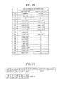
- FIG. 21 is a table for explaining the optical surface shape of an image-side scanning lens
- FIG. 22 is a table for explaining the optical surface shape of a collimator lens
- FIG. 23 is a diagram (No. 1) for explaining the positional relationship among major optical elements in an optical system shown in FIG. 2 ;
- FIG. 24 is a table (No. 2) for explaining the positional relationship among major optical elements in an optical system shown in FIG. 2 ;
- FIG. 25 is a table for explaining the optical surface shape of a deflector-side scanning lens in an optical system with another example structure
- FIG. 26 is a table for explaining the optical surface shape of an image-side scanning lens in an optical system with another example structure
- FIG. 27 is a table for explaining the positional relationship among major optical elements in an optical system with another example structure
- FIG. 28 is a graph for explaining the relationship between the amount of change in imaging position and temperature in an optical system with another example structure
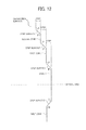
- FIG. 29 is a diagram of a first embodiment of a light-source unit
- FIG. 30A is a diagram of a second embodiment of a light-source unit
- FIG. 30B is a diagram of a third embodiment of a light-source unit.
- FIG. 31 is a schematic diagram of an exemplary structure of a tandem color printer.
- FIG. 1 is a schematic diagram of a laser printer 1000 as an image forming apparatus according to the present invention.
- the laser printer 1000 includes an optical scanning device 1010 according to a first embodiment of the present invention, a photosensitive drum 1030 , a charging unit 1031 , a developing roller 1032 , a transfer charging unit 1033 , a neutralizing unit 1034 , a cleaning unit 1035 , a toner cartridge 1036 , a feed roller 1037 , a feed tray 1038 , a pair of registration rollers 1039 , a fixing roller 1041 , a discharge roller 1042 , a discharge tray 1043 , a communication control unit 1050 , a printer control unit 1060 that controls each of the components, and so forth. These components are arranged at predetermined positions in a printer casing 1044 .
- the communication control unit 1050 controls a bi-directional communication with an upper-level device (e.g., a personal computer (PC)) via a network.
- an upper-level device e.g., a personal computer (PC)
- the photosensitive drum 1030 is a cylindrical member having a photosensitive layer formed on the surface thereof.
- the surface of the photosensitive drum 1030 is a scanning surface to be scanned.
- the photosensitive drum 1030 rotates in the direction indicated by the arrow shown in FIG. 1 .
- the charging unit 1031 , the developing roller 1032 , the transfer charging unit 1033 , the neutralizing unit 1034 , and the cleaning unit 1035 are arranged near the surface of the photosensitive drum 1030 . More specifically, they are arranged in following order along the rotational direction of the photosensitive drum 1030 : the charging unit 1031 ⁇ the developing roller 1032 ⁇ the transfer charging unit 1033 ⁇ the neutralizing unit 1034 ⁇ the cleaning unit 1035 .
- the charging unit 1031 uniformly charges the surface of the photosensitive drum 1030 .
- the optical scanning device 1010 irradiates the surface of the photosensitive drum 1030 charged by the charging unit 1031 with a light beam modulated based on image information from the upper-level device. By doing so, a latent image corresponding to the image information is formed on the surface of the photosensitive drum 1030 .
- the formed latent image moves towards the developing roller 1032 along with the rotation of the photosensitive drum 1030 .
- Toner stored in the toner cartridge 1036 is supplied to the developing roller 1032 .
- the developing roller 1032 applies the toner supplied from the toner cartridge 1036 onto the latent image formed on the surface of the photosensitive drum 1030 to make the image information a visual image.
- the latent image having the toner applied thereon (hereinafter, also referred to as “a toner image” for the sake of convenience) moves towards the transfer charging unit 1033 along with the rotation of the photosensitive drum 1030 .
- Recording sheets 1040 are stored in the feed tray 1038 .
- the feed roller 1037 Near the feed tray 1038 is the feed roller 1037 , which takes the recording sheets 1040 out of the feed tray 1038 one at a time and transports the recording sheet 1040 to the registration rollers 1039 .
- the registration rollers 1039 temporarily holds the recording sheet 1040 taken out by the feed roller 1037 and feeds the recording sheet 1040 to between the photosensitive drum 1030 and the transfer charging unit 1033 along with the rotation of the photosensitive drum 1030 .
- a voltage of opposite polarity to that of the toner is applied to the transfer charging unit 1033 to electrically transfer the toner on the surface of the photosensitive drum 1030 onto the recording sheet 1040 .
- the toner image on the surface of the photosensitive drum 1030 is transferred to the recording sheet 1040 .
- the recording sheet 1040 with the transferred toner is sent to the fixing roller 1041 .
- the fixing roller 1041 applies heat and pressure to the recording sheet 1040 , thereby causing the toner to be fixed on the recording sheet 1040 .
- the recording sheets 1040 on which toner has been fixed in this manner are sent to the discharge tray 1043 via the discharge roller 1042 and are stacked on the discharge tray 1043 sequentially.
- the neutralizing unit 1034 neutralizes the surface of the photosensitive drum 1030 .
- the cleaning unit 1035 removes any toner (residual toner) remaining on the surface of the photosensitive drum 1030 after transferring the toner image.
- the surface of the photosensitive drum 1030 from which the residual toner has been removed returns to a position facing the charging unit 1031 .
- the structure of the optical scanning device 1010 will now be described.
- the optical scanning device 1010 includes two light sources ( 14 a and 14 b ), two coupling lenses ( 15 a and 15 b ), two aperture plates ( 16 a and 16 b ), a cylindrical lens 17 , a reflecting mirror 18 , a polygon mirror 13 , a deflector-side scanning lens 11 a , an image-side scanning lens 11 b , a scan control apparatus (not shown in the figure), and so forth. These components are installed at predetermined positions in a housing 30 .
- the direction along the longitudinal direction of the photosensitive drum 1030 is the Y-axis direction and the direction along the optical axis of the scanning lenses ( 11 a and 11 b ) is the X-axis direction in the XYZ three-dimensional Cartesian coordinate system.
- the direction corresponding to the main-scanning direction is referred to as “a direction corresponding to the main scanning” and the direction corresponding to the sub-scanning direction is referred to as “a direction corresponding to the sub-scanning” for the sake of convenience.
- the light source 14 a includes an LD array 100 a having two light-emitting units arranged along the longitudinal direction.
- the Ma direction represents the direction corresponding to main scanning
- the Sa direction represents the direction corresponding to sub-scanning (same as the Z-axis direction in the embodiment).
- the Wa direction represents the exit direction of maximum intensity of a light beam from each of the light-emitting units.
- the distance D between the light-emitting units along the longitudinal direction is larger than the distance d between the light-emitting units in a case where the spacing p between neighboring scanning lines on the surface of the photosensitive drum 1030 gives half the desired resolution (1200 dpi in the embodiment).
- the distance between the light-emitting units refers to the center-to-center distance between the two light-emitting units.
- the distance between the light-emitting units in the Sa direction is set to d, which is given by rotating the LD array 100 a about an axis that passes through the center of the LD array 100 a and is parallel to the Wa direction.
- the rotational angle ⁇ of the LD array 100 a in this case is 55.5°.
- the light source 14 b includes, for example, an LD array 100 b similar to the LD array 100 a .
- the Mb direction represents the direction corresponding to main scanning
- the Sb direction represents the direction corresponding to sub-scanning (same as the Z-axis direction in the embodiment).
- the Wb direction represents the exit direction of maximum intensity of a light beam from each of the light-emitting units.
- the LD array 100 b is rotated by angle ⁇ (55.5° in the embodiment) about an axis that passes through the center of the LD array 100 b and is parallel to the Wb direction.
- the distance between the light-emitting units in the Sb direction after rotation is set to d.
- the spacing p between neighboring scanning lines on the surface of the photosensitive drum 1030 gives a resolution that is half the desired resolution (1200 dpi in the embodiment).
- the surface of the photosensitive drum 1030 can be scanned simultaneously with four light beams.
- the light source 14 a and the light source 14 b are disposed, for example, in the direction corresponding to sub-scanning (same as the Z-axis direction in the embodiment) such that the four light-emitting units are arranged at regular intervals d/2 when they are orthogonally projected onto an imaginary line extending in the direction corresponding to sub-scanning.
- the spacing between neighboring scanning lines on the surface of the photosensitive drum 1030 gives the desired resolution (1200 dpi in the embodiment).
- Reference numerals La 1 and La 2 in FIG. 6 denote the scanning lines of two light beams from the light source 14 a
- reference numerals Lb 1 and Lb 2 denote the scanning lines of two light beams from the light source 14 b.
- the light source 14 a and the light source 14 b are disposed such that the angle (crossing angle) between the Wa direction and the Wb direction is, for example, ⁇ (3.1° in the embodiment) on the XY plane.
- Each of the light-emitting units is an edge-emitting laser with a design oscillation wavelength of 655 nm.
- the coupling lens 15 a is disposed in the light path of the light beam from the light source 14 a . Furthermore, the coupling lens 15 b is disposed in the light path of the light beam from the light source 14 b.
- Each of the coupling lenses converts the light beam from the corresponding light source into substantially collimated light.
- the light beam from the corresponding light source is converted into a light beam shape suitable for the subsequent optical systems.
- a suitable light beam shape can be a collimated light beam, a weakly diverging light beam, or a weakly converging light beam.
- the positions of the coupling lenses can be adjusted individually in the optical-axis direction, the direction corresponding to main scanning, and the direction corresponding to sub-scanning.
- the position of each coupling lens is adjusted separately according to the oscillation wavelength of the corresponding LD array so that a shift in imaging position resulting from variation in oscillation wavelength across the LD arrays becomes small.
- Each of the coupling lenses is a glass lens with a focal length f of 27 mm at the design wavelength.
- this glass has the following physical properties: the refractive index for 655-nm light is 1.57719 at standard temperature (25° C.), the refractive index for 655-nm light when the temperature is increased by 20° C. from the standard temperature is 1.57727, and the linear expansion coefficient is 7.0 ⁇ 10 ⁇ 6 /K.
- Each of the coupling lenses includes a refractive surface as an output plane (see FIG. 8 ).
- This refractive surface is a rotationally symmetric aspherical surface with a paraxial radius of curvature of ⁇ 15.6 mm.
- Each of the coupling lenses includes a diffraction surface as an incidence plane (see FIG. 8 ).
- this diffraction surface is generated by combining a surface exhibiting a diffraction effect (hereinafter, also referred to as “a first surface” for the sake of convenience) and a surface exhibiting a refraction effect (hereinafter, also referred to as “a second surface” for the sake of convenience).
- the diffraction surface is set such that the power of the first surface and the power of the second surface offset each other. Therefore, the diffraction surface of each coupling lens exhibits no power from a geometrical-optics standpoint.
- a plurality of diffraction grooves on the diffraction surface of each coupling lens form concentric circular steps having the centers thereof aligned with the optical axis (see FIG. 9 ).
- a plurality of multi-level diffraction grooves are formed on the diffraction surface of each of the coupling lenses 15 .
- each of the steps is 1.135 ⁇ m.
- the minimum pitch (outermost zone) is 72.523 ⁇ m, and the number of steps is 20.
- each of the coupling lenses is endowed with more intense diffraction power than diffraction power required for correction of chromatic aberration at normal temperature.
- the diffraction power of each coupling lens is set to perform overcorrection.
- FIG. 10 is a graph showing the amount of change in imaging position along the main-scanning direction on the surface of the photosensitive drum 1030 when the environmental temperature is 10° C., 45° C., and 60° C. As is apparent from this graph, the amount of change in the imaging position is within 0.20 mm, which ensures that sufficient temperature compensation is performed.
- FIG. 11 is a graph showing a comparative example where no diffraction surface is provided. The amount of change in imaging position in this case reaches almost 2.00 mm, which indicates that it is difficult to maintain superior imaging quality.
- the diffraction surface has a shape formed by folding the shape of a refractive surface with appropriate steps and pitches, the pitches gradually become smaller towards the outer edge of the lens. Therefore, it is difficult to make a mold for forming the diffraction surface.
- the diffraction surface is formed by combining the first surface and the second surface having opposite power to each other, the zone surfaces are substantially orthogonal to the optical axis. This makes shape measurement easy.
- the zone surfaces are orthogonal to the optical axis.
- the angles ⁇ between the zone surfaces and the step surfaces neighboring the zone surfaces on a cross-sectional plane including the optical axis are all obtuse angles. More specifically, to build steps with a height of 1.135 ⁇ m in the optical-axis direction between zone surfaces, each of the step surfaces has a width of about 6 ⁇ m in the height direction, and the angle ⁇ between each zone surface and the neighboring step surface is 165°.
- a coupling lens is produced by molding. Because the angle ⁇ is an obtuse angle in each of the coupling lenses according to the embodiment, a sufficiently large draft is provided. Therefore, the molded product is easy to remove from the mold, thereby enhancing the molding performance.
- the angle ⁇ should preferably be larger than 135° and smaller than 170°.
- the multi-step diffraction surface exhibits no power from a geometrical-optics standpoint, the system is immune to a shift in the center of the incidence plane and the center of the output plane. This eliminates the need to achieve extremely high accuracy and allows a low-cost manufacturing process to be adopted.
- the far-field pattern (FFP) of the light beam emitted from an edge-emitting laser diode (LD) is typically elliptical.
- the divergence angle (half width) is 19° in the long-axis direction and 9° in the short-axis direction.
- a plurality of light-emitting units are normally arranged along the short-axis direction of the FFP (see FIG. 13A ).
- the reference state a state in which a plurality of light-emitting units are arranged along the direction corresponding to sub-scanning is referred to as the reference state for the sake of convenience.
- rotation of an LD array refers to rotation about a rotation axis that is parallel to the optical axis and passes through the center of the LD array.
- rotational angle refers to a rotational angle relative to the reference state. Therefore, the reference state is a state in which the rotational angle is 0°.
- the elliptical shape of the FFP When an LD array is rotated relative to the reference state, the elliptical shape of the FFP also rotates along with the rotation of the LD array, causing the elliptical shape of the FFP to change from the state shown in FIG. 13A to the state shown in FIG. 13B .
- FIG. 14A depicts the state of divergence of the light beam from an LD array on a plane orthogonal to the direction corresponding to sub-scanning in a case where the elliptical shape of the FFP is as shown in FIG. 13A .
- FIG. 14B depicts the state of divergence of the light beam from an LD array on a plane orthogonal to the direction corresponding to sub-scanning in a case where the elliptical shape of the FFP is as shown in FIG. 13B .
- the apodization can be prevented from becoming worse by increasing the focal length f of the coupling lens.
- the focal length f of the coupling lens should preferably satisfy Inequality (3) below using the thickness T of the coupling lens. 0.08 ⁇ T/f ⁇ 0.16 (3)
- T/f is 0.16 or more, that is, if the thickness is large, costs increase. If T/f is 0.08 or less, the amount of light is insufficient.
- the thickness of the coupling lens significantly affects costs and the light transmittance, a good balance can be established among low costs, the light transmittance, and the amount of light by satisfying Inequality (3) above.
- the thickness of the coupling lens is set to 2.5 mm, and the focal length at the design wavelength is set to 27 mm.
- FIG. 16 is a graph showing so-called depth of spot size of a light beam focused onto the surface of the photosensitive drum 1030 when an LD array is in the reference state.
- depth of spot size refers to the amount of defocus in which a beam spot size of 50 ⁇ m or less is maintained with any image height.
- FIG. 17 is a graph showing the depth of spot size as obtained by rotating the LD array by 70° relative to the reference state.
- the depth of spot size becomes small with the rotation of the LD array.
- each of the coupling lenses is endowed with diffraction power high enough to compensate for a change in imaging position due to a temperature change, as described above, the required depth of spot size can be achieved even when the LD array is rotated relative to the reference state.
- the light reflected at the multi-step diffraction surface returns via the same light path as that of the incident light because the multi-step diffraction surface exhibits no power from a geometrical-optics standpoint.
- FIG. 18B for example, when uncollimated light is incident upon the multi-step diffraction surface, the light reflected at the multi-step diffraction surface becomes a diverging light beam.
- the output plane of the coupling lens is formed as a multi-step diffraction surface
- the reflected light from the multi-step diffraction surface returns to the light source via the same light path as that of the incident light, because the light beam from the light source is converted into a collimated light beam before it reaches the output plane.
- This return light causes the output from the light source to be unstable, acting as a factor that degrades the image quality.
- each of the coupling lenses is formed as a multi-step diffraction surface, for example, as shown in FIG. 19B , the reflected light from the multi-step diffraction surface is converted into a diverging light beam. Therefore, there is no risk of making the output from the light source unstable.
- each of the coupling lenses has an edge portion around an outer circumference thereof (see FIG. 8 ), and the transmittance of ultraviolet light at the edge portion is at least 30%. Because of this, after adjustment, the coupling lens can be bonded, for example, on an LD unit with UV curable resin. For this reason, a supporting mechanism that holds the coupling lens is not necessary, which contributes to a further reduction in cost.
- the aperture plate 16 a includes an aperture portion to specify the beam diameter of a light beam that has passed through the coupling lens 15 a .
- the aperture plate 16 b includes an aperture portion to specify the beam diameter of a light beam that has passed through the coupling lens 15 b.
- the cylindrical lens 17 focuses, in the direction corresponding to sub-scanning (the Z-axis direction in the embodiment), the light beam that has passed through the aperture portion of each aperture plate onto a point near the deflecting reflection surface of the polygon mirror 13 via the reflecting mirror 18 .
- the cylindrical lens 17 is made of glass that has the following physical properties: the refractive index for 655-nm light is 1.5144 at standard temperature (25° C.) and the linear expansion coefficient is 7.5 ⁇ 10 ⁇ 6 /K.
- the incidence plane of the cylindrical lens 17 is a cylindrical surface with a paraxial radius of curvature of 36.1 mm in the direction corresponding to sub-scanning (the Z-axis direction in the embodiment).
- the optical system disposed in the light path between each of the light sources and the polygon mirror 13 is also referred to as a pre-deflector optical system.
- the pre-deflector optical system includes the two coupling lenses ( 15 a and 15 b ), the two aperture plates ( 16 a and 16 b ), the cylindrical lens 17 , and the reflecting mirror 18 .
- Soundproof glass 21 is disposed between the reflecting mirror 18 and the polygon mirror 13 and between the polygon mirror 13 and the deflector-side scanning lens 11 a.
- the polygon mirror 13 includes, for example, a hexagonal mirror unit whose inscribed circle has a radius of 18 mm, and the mirrors each function as a deflecting reflection surface.
- the polygon mirror 13 deflects the light beam from the reflecting mirror 18 while rotating at a constant speed about an axis parallel to the direction corresponding to sub-scanning (the Z-axis direction in the embodiment).
- the incident angle of the light beam from the light source 14 a upon the polygon mirror 13 is 56.45° relative to the direction corresponding to main scanning and 0° relative to the direction corresponding to sub-scanning. Furthermore, the incident angle of the light beam from the light source 14 b upon the polygon mirror 13 is 59.55° relative to the direction corresponding to main scanning and 0° relative to the direction corresponding to sub-scanning.
- the deflector-side scanning lens 11 a is arranged on the optical path of the light beam deflected by the polygon mirror 13 .
- the image-side scanning lens 11 b is arranged on the optical path of the light beam that has passed through the deflector-side scanning lens 11 a.
- the optical system disposed in the light path between the polygon mirror 13 and the photosensitive drum 1030 is also called a scanning optical system.
- the scanning optical system includes the deflector-side scanning lens 11 a and the image-side scanning lens 11 b.
- the light beam deflected at the polygon mirror 13 is focused onto the surface of the photosensitive drum 1030 by the scanning optical system.
- the light spot on the surface of the photosensitive drum 1030 moves in the longitudinal direction of the photosensitive drum 1030 along with the rotation of the polygon mirror 13 .
- the surface of the photosensitive drum 1030 is scanned.
- the moving direction of the light spot in this case corresponds to the “main-scanning direction”.
- dust-tight glass 22 is disposed between the image-side scanning lens 11 b and the photosensitive drum 1030 .
- Each of the scanning lenses is made of resin and has a larger degree of expansion/contraction resulting from a temperature change than that of a glass lens.
- This resin has the following physical properties: the refractive index for 655-nm light is 1.5273 at standard temperature and the linear expansion coefficient is 7.0 ⁇ 10 ⁇ 5 /K.
- the incidence plane (first surface) of the deflector-side scanning lens 11 a and each surface of the image-side scanning lens 11 b are a special toroidal surface.
- Each of the special toroidal surfaces is a surface whose curvature in the direction corresponding to sub-scanning changes according to the height of the lens in the direction corresponding to main scanning, represented as Equations (4) and (5) below.
- x represents a depth in the optical-axis direction
- R y represents a paraxial radius of curvature in the direction corresponding to main scanning (the Y-axis direction in the embodiment)
- the output plane (second surface) of the deflector-side scanning lens 11 a is a rotationally symmetric aspherical surface.
- the aspherical surface used in the embodiment is given by Equation (6) below
- FIG. 20 is a table showing values on the incidence plane (first surface) and the output plane (second surface) of the deflector-side scanning lens 11 a.
- FIG. 21 is a table showing values on the incidence plane (third surface) and the output plane (fourth surface) of the image-side scanning lens 11 b.
- FIG. 22 is a table showing values on the output plane of each of the coupling lenses.
- the lateral magnification of the scanning optical system in the sub-scanning direction is ⁇ 0.9879.
- the length (writing width in the main-scanning direction) of the effective scanning area on the photosensitive drum 1030 is 320 mm.
- the half angle of view is 36.1°.
- FIGS. 23 and 24 show specific positional relationships among major optical elements.
- the optical scanning device 1010 includes the two light sources ( 14 a and 14 b ), the pre-deflector optical system, the polygon mirror 13 , and the scanning optical system.
- the pre-deflector optical system includes the two coupling lenses ( 15 a and 15 b ), the two aperture plates ( 16 a and 16 b ), the cylindrical lens 17 , and the reflecting mirror 18 .
- Each of the coupling lenses has no power at room temperature and includes a multi-level diffraction surface having a plurality of zone surfaces substantially orthogonal to the optical axis and at least one step surface neighboring each of the zone surfaces.
- the angle between each of the zone surfaces and its neighboring step surface is an obtuse angle on a cross-sectional plane including the optical axis.
- each of the coupling lenses according to the embodiment is substantially equivalent to a planoconvex lens
- light-emitting units disposed far away from the optical axis can easily be corrected for aberration by forming a multi-step diffraction surface (substantially flat surface) on the coupling-lens surface upon which a diverging light beam is incident.
- each coupling lens can be rotationally symmetric with respect to the optical axis.
- ease of mold making is further enhanced, and a coupling lens can be produced via lower-cost processes.
- each coupling lens should also preferably be rotationally symmetric. By doing so, the need to consider rotation about the optical axis is eliminated at the time of assembly, and the work required for assembly can be reduced.
- a technique for using a plurality of LD elements each having one light-emitting unit to combine the light beams from the LD elements into multiple light beams may be employed.
- variation in oscillation wavelength across the LD elements is within a range of about ⁇ 10 nm, which is several times larger than the variation in oscillation wavelength across light-emitting units in one LD array.
- diffractive lenses with different light beam wavelengths cause different imaging positions, the variation in oscillation wavelength across LD elements is not negligible.
- One diffractive lens can be provided for each LD element if the coupling lens is realized by a diffractive lens. As a result, even if the oscillation wavelengths of a plurality of LD elements are different from one another, a desired light beam can be obtained according to the oscillation wavelength.
- the laser printer 1000 includes the optical scanning device 1010 that makes it possible to perform stable optical scanning without increasing costs, a high-quality image can be produced stably without bringing about high cost.
- each of the light sources includes two light-emitting units
- the number of light-emitting units is not limited to two.
- the rotational angle ⁇ of the LD array in each of the light sources is 55.5°
- the rotational angle ⁇ is not limited to 55.5°.
- the rotational angle ⁇ is determined according to the distance between the light-emitting units and the desired resolution in the LD array.
- the polygon mirror 13 includes the hexagonal mirror unit
- the polygon mirror 13 is not limited to a hexagonal mirror unit.
- the structure of the optical scanning device 1010 according to the embodiment described above is just one example, and the structure is not limited to this example. Another example structure that can be adopted for the optical scanning device 1010 will now be described briefly with reference to FIGS. 25 to 28 .
- the following description focuses only on differences from the embodiment described above. Components that are same as or similar to those in the embodiment described above are denoted by the same reference numerals, and a description thereof will be simplified or omitted.
- FIG. 28 is a graph showing the amount of change in imaging position along the main-scanning direction on the surface of the photosensitive drum 1030 at environmental temperatures of 10° C., 45° C., and 60° C. in this case. As is apparent from this graph, the amount of change in imaging position is within 0.20 mm, which ensures sufficient temperature compensation, as with the embodiment described above.
- each of the light sources and each of the coupling lenses may be combined into a light-source unit.
- FIG. 29 is a diagram of a first embodiment of the light-source unit.
- Semiconductor lasers ( 403 and 404 ) are individually fitted into two respective fitting holes (not shown in the figure) formed on the rear surface of a substrate 405 .
- the fitting holes are tilted relative to each other by a predetermined angle (about 1.5° in the embodiment) on a plane including the direction corresponding to main scanning.
- the semiconductor lasers fitted into the respective fitting holes are also tilted with respect to each other by a predetermined angle (about 1.5° in the embodiment) on a plane including the direction corresponding to main scanning.
- notches are formed in cylindrical heatsinks ( 403 - 1 and 404 - 1 ) of the semiconductor lasers.
- the array directions of the light sources are aligned by fitting protrusions ( 406 - 1 and 407 - 1 ) formed in the central round holes of holding members ( 406 and 407 ) to the notch portions of the heatsinks.
- Each of the semiconductor lasers is fixed on the substrate 405 by retaining the holding members ( 406 and 407 ) to the substrate 405 with screws 412 from the rear side thereof.
- each of coupling lenses ( 408 and 409 ) is carried out by fitting the outer circumferences of the coupling lenses ( 408 and 409 ) along semi-circular mounting guide surfaces ( 405 - 4 and 405 - 5 ) of the substrate 405 for appropriate positioning, so that the diverging light beam emitted from the light-emitting units becomes a collimated light beam.
- the fitting holes and the semi-circular mounting guide surfaces ( 405 - 4 and 405 - 5 ) are tilted along the direction of light beam.
- the substrate 405 is fixed to a holder 410 by bringing a cylindrical engaging portion 405 - 3 of the substrate 405 into engagement with the holder 410 and screwing a screw 413 into screw holes ( 405 - 6 and 405 - 7 ) through a through-hole 410 - 2 .
- a cylindrical portion 410 - 1 of the holder 410 is fitted into a reference hole 411 - 1 provided on a mounting wall 411 of an optical housing.
- the holder 410 is held in close contact with the rear side of the mounting wall 411 by inserting a spring 611 from the front side of the mounting wall 411 and bringing a stopper 612 into engagement with a protrusion 410 - 3 on the cylindrical portion, thus holding the light-source unit.
- Rotary force about the center of the cylindrical portion, serving as a rotation axis is exerted on the light-source unit by hooking one end of the spring 611 to a protrusion 411 - 2 on the mounting wall 411 and hooking the other end of the spring 611 to the light-source unit.
- An adjusting screw 613 is included to lock the rotary force of the light-source unit, and with the adjusting screw 613 , the entire unit can be made to turn about the optical axis ( ⁇ direction) for pitch adjustment.
- FIG. 30A is a diagram of a second embodiment of the light-source unit.
- reference numeral 706 denotes a holding member
- reference numeral 705 denotes a substrate
- reference numeral 710 denotes a holder.
- the second embodiment differs from the first embodiment in that only one semiconductor laser 703 is provided as the light source, and in accordance with the, only one holding member 706 is provided; other structures are basically the same.
- FIG. 30B is a diagram of a characteristic part of a third embodiment of the light-source unit.
- the third embodiment is similar to the second embodiment in structure; in the third embodiment, the light source includes a semiconductor laser array 801 with four light-emitting units. The light beams from the semiconductor laser array 801 are combined by the beam combining unit.
- the basic components according to the third embodiment are the same as those according to the first embodiment and the second embodiment, and a description thereof will be omitted.
- a vertical-cavity surface-emitting laser (VCSEL) array (surface-emitting laser array) may be used in place of the LD array.
- VCSEL vertical-cavity surface-emitting laser
- the image forming apparatus is not limited to a laser printer.
- any image forming apparatus including the optical scanning device 1010 can form high-quality images stably without increasing costs.
- an image forming apparatus in which media that develop color with a laser beam (e.g., paper sheet) are irradiated directly with a laser beam is also acceptable.
- media that develop color with a laser beam e.g., paper sheet
- a laser beam e.g., paper sheet
- an image forming apparatus in which silver-halide film is used as the image bearing member is also acceptable.
- a latent image is formed on the silver-halide film by optical scanning, and the latent image can be visualized through processing similar to a development process of the normal silver-halide photographic process. Thereafter, the visualized image can be transferred to printing paper through processing similar to printing of the normal silver-halide photographic process.
- Such an image forming apparatus can be realized as a photo-platemaking apparatus or a photo-imaging apparatus that produces, for example, CT scan images.
- image forming apparatuses that form multi-color images can form high-quality images at high speed without increasing costs by using an optical scanning device that supports color images.
- a color printer 2000 including a plurality of photosensitive drums is also acceptable, as shown in FIG. 31 .
- the color printer 2000 is a tandem multi-color printer that forms full-color images by overlapping four colors (black, cyan, magenta, and yellow).
- the color printer 2000 includes a photosensitive drum K 1 , a charging apparatus K 2 , a developing apparatus K 4 , a cleaning unit K 5 , and a transfer apparatus K 6 for black; a photosensitive drum C 1 , a charging apparatus C 2 , a developing apparatus C 4 , a cleaning unit C 5 , and a transfer apparatus C 6 for cyan; a photosensitive drum M 1 , a charging apparatus M 2 , a developing apparatus M 4 , a cleaning unit M 5 , and a transfer apparatus M 6 for magenta; a photosensitive drum Y 1 , a charging apparatus Y 2 , a developing apparatus Y 4 , a cleaning unit Y 5 , and a transfer apparatus Y 6 for yellow; an optical scanning device 2010 ; a conveyor belt 2080 ; a fixing unit 2030 ; and so forth.
- Each of the photosensitive drums rotates in the direction indicated by the corresponding arrow in FIG. 31 .
- a charging apparatus Around each of the photosensitive drums, a charging apparatus, a developing apparatus, a transfer apparatus, and a cleaning unit are arranged along the rotational direction.
- Each of the charging apparatuses uniformly charges the surface of the corresponding photosensitive drum.
- the surface of each of the photosensitive drums charged by the charging apparatus is irradiated with light from the optical scanning device 2010 , and an electrostatic latent image is formed on each of the photosensitive drums.
- a toner image is formed on the surface of each of the photosensitive drums by the corresponding developing apparatus.
- a toner image of each color is transferred onto a recording sheet by the corresponding transfer apparatus, and finally an image is fixed on the recording sheet by the fixing unit 2030 .
- the optical scanning device 2010 includes a light source similar to the light sources ( 14 a and 14 b ) described above, a pre-deflector optical system similar to the pre-deflector optical system described above, and a scanning optical system similar to the scanning optical system described above, for each color.
- the light beam from each of the light sources is deflected by a common deflector and emitted to the corresponding photosensitive drum via the corresponding scanning optical system.
- the optical scanning device 2010 includes a plurality of coupling lenses each having a diffraction surface with no power at room temperature.
- Each of the coupling lenses includes a multi-level diffraction surface having a plurality of zone surfaces substantially orthogonal to the optical axis and at least one step surface neighboring each of the zone surfaces.
- the angle between each of the zone surfaces and its neighboring step surface is an obtuse angle on a cross-sectional plane including the optical axis.
- the optical scanning device 2010 can afford similar advantages to those of the optical scanning device 1010 .
- the color printer 2000 can form high-quality color images stably without increasing costs.
- the optical scanning device 1010 described above may be employed for each color in place of the optical scanning device 2010 described above.
Abstract
Description
φ(H)=C H ·H 2 (1)
where CH=−1.519×10⁻³ (mm−1).
x(H)=(1/2R)·H 2 (2)
where the radius of curvature is, for example, R=−190 mm.
0.08<T/f<0.16 (3)
where x represents a depth in the optical-axis direction, Ry represents a paraxial radius of curvature in the direction corresponding to main scanning (the Y-axis direction in the embodiment), Rz represents a paraxial radius of curvature in the direction corresponding to sub-scanning (the Z-axis direction in the embodiment), y represents a distance from the optical axis in the direction corresponding to main scanning, z represents a distance from the optical axis in the direction corresponding to sub-scanning, K represents a conic constant, and A4, A6, A8, A10, A12, B1, B2, B3, . . . are all coefficients.
where C is the reciprocal of the paraxial radius of curvature (paraxial curvature) and H is the height from the optical axis.
- (1) The rotational angle α of the LD array in each of the light sources is 70.6°. Furthermore, the incident angle of the light beam from the
light source 14 a upon thepolygon mirror 13 is 62.45° relative to the direction corresponding to main scanning and 0° relative to the direction corresponding to sub-scanning. In addition, the incident angle of the light beam from thelight source 14 b upon thepolygon mirror 13 is 65.55° relative to the direction corresponding to main scanning and 0° relative to the direction corresponding to sub-scanning. - (2) For each of the coupling lenses, CH=−1.560×10⁻³, and the radius of curvature R of the second surface is −185 mm (R=−185 mm). Furthermore, the size of each of the multiple steps is 1.135 μm. The minimum pitch (outermost zone) is 69.878 μm, and the number of steps is 21.
- (3) The
polygon mirror 13 includes a tetragonal mirror unit whose inscribed circle has a radius of 8 mm. - (4)
FIG. 25 is a table showing values on the incidence plane (first surface) and the output plane (second surface) of the deflector-side scanning lens 11 a. - (5)
FIG. 26 is a table showing values on the incidence plane (third surface) and the output plane (fourth surface) of the image-side scanning lens 11 b. - (6)
FIG. 27 is a table showing one example of specific values (in units of mm) of reference numerals d1 to d10.
Claims (16)
Applications Claiming Priority (2)
| Application Number | Priority Date | Filing Date | Title |
|---|---|---|---|
| JP2008-020019 | 2008-01-31 | ||
| JP2008020019A JP5022253B2 (en) | 2008-01-31 | 2008-01-31 | Optical scanning apparatus and image forming apparatus |
Publications (2)
| Publication Number | Publication Date |
|---|---|
| US20090214261A1 US20090214261A1 (en) | 2009-08-27 |
| US8624951B2 true US8624951B2 (en) | 2014-01-07 |
Family
ID=40998453
Family Applications (1)
| Application Number | Title | Priority Date | Filing Date |
|---|---|---|---|
| US12/362,050 Active 2030-04-24 US8624951B2 (en) | 2008-01-31 | 2009-01-29 | Optical scanning device and image forming apparatus |
Country Status (2)
| Country | Link |
|---|---|
| US (1) | US8624951B2 (en) |
| JP (1) | JP5022253B2 (en) |
Families Citing this family (9)
| Publication number | Priority date | Publication date | Assignee | Title |
|---|---|---|---|---|
| JP5316759B2 (en) * | 2008-10-16 | 2013-10-16 | 株式会社リコー | Optical scanning device, adjustment method, and image forming apparatus |
| JP2010197990A (en) * | 2009-02-02 | 2010-09-09 | Ricoh Co Ltd | Optical scanning device, image forming apparatus, control method and program |
| JP5691528B2 (en) | 2011-01-07 | 2015-04-01 | 株式会社リコー | Optical scanning apparatus and image forming apparatus |
| JP2012145823A (en) * | 2011-01-13 | 2012-08-02 | Ricoh Co Ltd | Optical scanning device and image forming device |
| JP5896215B2 (en) | 2012-01-24 | 2016-03-30 | 株式会社リコー | Optical scanning apparatus and image forming apparatus |
| JP6244663B2 (en) | 2012-07-05 | 2017-12-13 | 株式会社リコー | Optical scanning apparatus and image forming apparatus |
| JP6351257B2 (en) * | 2013-12-26 | 2018-07-04 | キヤノン株式会社 | Optical scanning device and image forming apparatus having the same |
| JP6492966B2 (en) | 2015-05-22 | 2019-04-03 | 株式会社リコー | Light source unit and image display device |
| CN105005152B (en) * | 2015-07-17 | 2018-03-09 | 北京空间机电研究所 | A kind of wide spectrum diffraction optics imaging system |
Citations (90)
| Publication number | Priority date | Publication date | Assignee | Title |
|---|---|---|---|---|
| US5557448A (en) | 1994-06-28 | 1996-09-17 | Ricoh Company, Ltd. | Optical scanner |
| US5570224A (en) | 1993-04-08 | 1996-10-29 | Ricoh Company, Ltd. | Optical scanning apparatus |
| US5581392A (en) | 1993-10-13 | 1996-12-03 | Ricoh Company, Ltd. | Optical Scanner |
| US5652670A (en) | 1995-03-01 | 1997-07-29 | Ricoh Company, Ltd. | Scanning image forming lens and optical scanner |
| US5875051A (en) | 1995-10-25 | 1999-02-23 | Ricoh Company, Ltd. | Optical scanning device and a scanning lens therefor |
| US6069724A (en) | 1997-02-17 | 2000-05-30 | Ricoh Company, Ltd. | Optical scanning lens and optical scanning apparatus |
| JP2000171741A (en) | 1998-12-08 | 2000-06-23 | Fuji Photo Optical Co Ltd | Optical scanner |
| US6081386A (en) | 1997-04-15 | 2000-06-27 | Ricoh Company, Ltd. | Optical scanning lens, optical scanning and imaging system and optical scanning apparatus incorporating same |
| US6104522A (en) | 1996-09-13 | 2000-08-15 | Ricoh Company, Ltd. | Optical scanning apparatus with controlled sag and ghost |
| US6185026B1 (en) | 1998-08-06 | 2001-02-06 | Ricoh Company, Ltd. | Multi-beam scanning apparatus |
| US6198562B1 (en) | 1999-03-03 | 2001-03-06 | Ricoh Co., Ltd. | Multi-beam scanning device and image forming system and method using the same |
| US20020036827A1 (en) * | 2000-09-27 | 2002-03-28 | Takehiko Nakai | Diffractive optical element and optical system having the same |
| US6369927B2 (en) | 1998-02-13 | 2002-04-09 | Ricoh Company, Ltd. | Optical scanning apparatus |
| US6400391B1 (en) | 1999-06-09 | 2002-06-04 | Ricoh Company, Ltd. | Optical scanning lens, optical scanning device and image forming apparatus |
| US6404530B1 (en) * | 1999-10-28 | 2002-06-11 | Asahi Kogaku Kogyo Kabushiki Kaisha | Scanning optical system |
| JP2002287062A (en) | 2001-03-26 | 2002-10-03 | Minolta Co Ltd | Laser scanner |
| US6462853B2 (en) | 2000-04-05 | 2002-10-08 | Ricoh Company, Ltd. | Optical scanning device |
| US20020149668A1 (en) * | 2001-01-29 | 2002-10-17 | Manabu Kato | Scanning optical device and image forming apparatus using the same |
| US20030053156A1 (en) | 2001-08-20 | 2003-03-20 | Yukito Satoh | Optical scanning device and image forming apparatus using the same |
| US6587245B2 (en) | 2000-07-24 | 2003-07-01 | Ricoh Company, Ltd. | Optical scanning device, optical scanning method, and image forming apparatus |
| US6657765B2 (en) | 2001-03-01 | 2003-12-02 | Ricoh Company, Ltd. | Optical deflecting unit, optical scanning unit, image forming apparatus, and method of producing optical unit |
| US20040036936A1 (en) | 2002-07-02 | 2004-02-26 | Tomohiro Nakajima | Optical scanner and image forming apparatus |
| US6757089B2 (en) | 2000-09-08 | 2004-06-29 | Ricoh Company, Ltd. | Optical scanning device having a deflection mirror to scan a scanned surface at a constant velocity via a light beam to obtain a large effective write width |
| US20040136043A1 (en) * | 2002-12-26 | 2004-07-15 | Pentax Corporation | Scanning optical system |
| US6768506B2 (en) | 2000-10-27 | 2004-07-27 | Ricoh Company, Ltd. | Image formation with a reduced recording position deviation between scanning optical systems |
| US6771407B2 (en) | 2001-09-20 | 2004-08-03 | Ricoh Company, Ltd. | Optical scanner and image formation apparatus |
| US6771296B2 (en) | 2000-10-03 | 2004-08-03 | Ricoh Company, Ltd. | Optical scanning device and method for providing specific dot offsets at center and ends of scan width |
| US6788444B2 (en) | 2001-10-24 | 2004-09-07 | Ricoh Company, Ltd. | Method and apparatus for optical scanning capable of reducing a dot position displacement and a dot diameter variation |
| US6803941B2 (en) | 2000-02-03 | 2004-10-12 | Ricoh Company, Ltd. | Image forming apparatus with overlapped light fluxes forming a dot |
| US6804064B2 (en) | 2002-10-23 | 2004-10-12 | Ricoh Company, Ltd. | Zoom lens, camera, and portable information terminal apparatus |
| US6829102B2 (en) | 2002-03-20 | 2004-12-07 | Ricoh Company, Ltd. | Zoom lens, and camera and portable information terminal for utilizing zoom lens |
| US6903856B2 (en) | 2000-12-28 | 2005-06-07 | Ricoh Company, Ltd. | Optical scanning device decreasing amount of change in relative scanning position |
| US6906739B2 (en) | 2002-03-01 | 2005-06-14 | Ricoh Company, Ltd. | Optical scanner and imaging apparatus using the same |
| US6934061B2 (en) | 2002-08-28 | 2005-08-23 | Ricoh Company, Ltd. | Optical scanner and image reproducing apparatus |
| US20050201219A1 (en) * | 2004-01-23 | 2005-09-15 | Tooru Hotsuta | Optical head device |
| US6956685B2 (en) | 2000-05-19 | 2005-10-18 | Ricoh Company, Ltd. | Multi-beam scanner, multi-beam scanning method, synchronizing beam detecting method and image forming apparatus |
| US20050243396A1 (en) | 2004-04-12 | 2005-11-03 | Mitsumi Fujii | Deflector mirror, optical scanning device, and image forming apparatus |
| US20050265151A1 (en) * | 2004-05-27 | 2005-12-01 | Konica Minolta Opto, Inc. | Objective optical system, optical pickup apparatus and optical disk drive apparatus |
| US6987593B2 (en) | 2002-03-08 | 2006-01-17 | Ricoh Company, Ltd. | Optical scanning device and image forming apparatus using the same |
| US7006120B2 (en) | 2002-08-07 | 2006-02-28 | Ricoh Company, Ltd. | Multi-beam optical scanning apparatus and image forming apparatus |
| US7050210B2 (en) | 2002-05-01 | 2006-05-23 | Ricoh Company, Ltd. | Optical scanning device and imaging apparatus implementing the same |
| US7068296B2 (en) | 2001-09-14 | 2006-06-27 | Ricoh Company, Ltd. | Optical scanning device for reducing a dot position displacement at a joint of scanning lines |
| US7088484B2 (en) | 2002-03-25 | 2006-08-08 | Ricoh Company, Inc. | Optical scanning method and system capable of performing high speed scanning and high resolution, and image forming apparatus having the optical scanning system |
| US7106483B2 (en) | 2003-06-12 | 2006-09-12 | Ricoh Company, Limited | Optical scanner and image forming apparatus |
| US20060232659A1 (en) | 2005-03-31 | 2006-10-19 | Yoshinori Hayashi | Optical scanning device and image forming apparatus |
| US20060239312A1 (en) * | 2005-04-23 | 2006-10-26 | Telaris Inc. | Semiconductor Lasers in Optical Phase-Locked Loops |
| US20060245009A1 (en) | 2005-04-07 | 2006-11-02 | Hiroshi Akiyama | Optical scanning device and image forming apparatus |
| US7145705B2 (en) | 2003-09-19 | 2006-12-05 | Ricoh Company, Limited | Optical scanner and image forming apparatus |
| US20060284968A1 (en) | 2005-06-20 | 2006-12-21 | Yoshinori Hayashi | Optical scanning device and image forming apparatus |
| US20070002417A1 (en) | 2005-06-29 | 2007-01-04 | Makoto Hirakawa | Optical scanning device and image forming apparatus |
| US20070030538A1 (en) | 2005-08-04 | 2007-02-08 | Makoto Hirakawa | Optical scanning apparatus and image forming apparatus |
| US20070058255A1 (en) | 2005-09-09 | 2007-03-15 | Shigeaki Imai | Optical scanner and image forming apparatus |
| US20070064291A1 (en) * | 2005-09-16 | 2007-03-22 | Fuji Xerox Co., Ltd. | Optical scanning apparatus |
| US7218432B2 (en) | 2005-06-20 | 2007-05-15 | Ricoh Company, Limited. | Optical scanning apparatus and image forming apparatus |
| US7236281B2 (en) | 2003-02-27 | 2007-06-26 | Ricoh Company, Limited. | Optical scanner and image forming apparatus |
| US7253937B2 (en) | 2005-10-20 | 2007-08-07 | Ricoh Company, Ltd. | Multi-beam optical scanning device and image forming apparatus |
| US20070211324A1 (en) | 2006-03-13 | 2007-09-13 | Ricoh Company, Limited | Optical scanning device and image forming apparatus |
| JP2007233002A (en) | 2006-02-28 | 2007-09-13 | Ricoh Co Ltd | Optical scanning device and image forming apparatus |
| US7271823B2 (en) | 2003-08-29 | 2007-09-18 | Ricoh Company, Ltd. | Optical scanner and image forming apparatus |
| US7271824B2 (en) | 2001-09-28 | 2007-09-18 | Ricoh Company, Ltd. | Pixel clock generating apparatus, optical writing apparatus using a pixel clock, imaging apparatus, and method for generating pixel clocks |
| JP2007241182A (en) | 2006-03-13 | 2007-09-20 | Ricoh Co Ltd | Optical scanner and image forming apparatus |
| US20070253048A1 (en) | 2006-04-27 | 2007-11-01 | Kohji Sakai | Optical scanning device, optical writing device, and image forming apparatus |
| JP2007293182A (en) | 2006-04-27 | 2007-11-08 | Ricoh Co Ltd | Optical scanner, optical write-in apparatus and image forming apparatus |
| US20070297036A1 (en) | 2006-06-21 | 2007-12-27 | Tadashi Nakamura | Optical scanning apparatus and image forming apparatus |
| US20080024849A1 (en) | 2006-07-24 | 2008-01-31 | Yoshinori Hayashi | Optical scanning apparatus and image forming apparatus |
| US20080025759A1 (en) | 2006-07-27 | 2008-01-31 | Ichii Daisuke | Optical scanning device and image forming apparatus |
| US20080062491A1 (en) | 2006-09-07 | 2008-03-13 | Tadashi Nakamura | Light-source device, optical scanning device, and image forming apparatus |
| US20080068693A1 (en) | 2006-09-19 | 2008-03-20 | Yoshinori Hayashi | Optical scanner and image forming apparatus using optical scanner |
| US20080068689A1 (en) | 2006-09-15 | 2008-03-20 | Kenichiro Saisho | Diffractive-optical element, scanning optical system, optical scanner, and image forming apparatus |
| US7362486B2 (en) | 2004-09-29 | 2008-04-22 | Ricoh Company, Ltd. | Optical scanning device with at least one resin lens for controlling a beam waist position shift |
| US20080100920A1 (en) * | 2006-10-30 | 2008-05-01 | Kyocera Mita Corporation | Optical scanning device and image forming apparatus having the same |
| US20080100895A1 (en) | 2006-10-25 | 2008-05-01 | Yoshinori Hayashi | Scanning unit and image forming apparatus |
| US20080123159A1 (en) | 2006-11-24 | 2008-05-29 | Yoshinori Hayashi | Scanning unit and image forming apparatus |
| US7385181B2 (en) | 2006-03-14 | 2008-06-10 | Ricoh Company, Ltd. | Optical scanning device and image forming device |
| US20080180772A1 (en) | 2007-01-31 | 2008-07-31 | Naoki Miyatake | Optical scanning device and image forming apparatus |
| US20080192319A1 (en) | 2007-02-09 | 2008-08-14 | Naoki Miyatake | Optical scanning device and image forming apparatus |
| US7417777B2 (en) | 2006-09-04 | 2008-08-26 | Ricoh Company, Ltd. | Optical scanning device and image forming apparatus |
| US20080204842A1 (en) | 2007-02-27 | 2008-08-28 | Nobuyuki Arai | Optical scanning device and image forming apparatus |
| US20080204840A1 (en) | 2007-02-28 | 2008-08-28 | Naoto Watanabe | Optical scanning device and image forming apparatus |
| US20080204841A1 (en) | 2007-02-22 | 2008-08-28 | Seizo Suzuki | Optical scanning device and image forming apparatus |
| US20080212999A1 (en) | 2007-03-02 | 2008-09-04 | Kensuke Masuda | Light-amount detecting device, light source device, optical scanning unit and image forming apparatus |
| US20080218827A1 (en) | 2007-03-09 | 2008-09-11 | Naoto Watanabe | Optical scanning device and image forming apparatus |
| US20080219601A1 (en) | 2007-03-07 | 2008-09-11 | Nobuyuki Arai | Optical scanner and image forming apparatus |
| US20080267663A1 (en) | 2007-04-26 | 2008-10-30 | Ichii Daisuke | Optical scanning device and image forming apparatus |
| US20080266633A1 (en) | 2007-04-24 | 2008-10-30 | Makoto Hirakawa | Optical scanning device and image forming apparatus |
| US20080267662A1 (en) | 2007-04-24 | 2008-10-30 | Nobuyuki Arai | Light scanning device and image forming apparatus |
| US20080284838A1 (en) | 2007-05-14 | 2008-11-20 | Seizo Suzuki | Optical scan apparatus and image formation apparatus |
| US20080285104A1 (en) | 2007-05-14 | 2008-11-20 | Nobuyuki Arai | Optical scanner and image forming apparatus |
| US7471434B2 (en) | 2006-09-01 | 2008-12-30 | Ricoh Company, Ltd. | Optical scanning device and image forming apparatus |
| US20090060582A1 (en) | 2007-09-04 | 2009-03-05 | Ichii Daisuke | Optical scanning device and method for adjusting errors |
-
2008
- 2008-01-31 JP JP2008020019A patent/JP5022253B2/en not_active Expired - Fee Related
-
2009
- 2009-01-29 US US12/362,050 patent/US8624951B2/en active Active
Patent Citations (93)
| Publication number | Priority date | Publication date | Assignee | Title |
|---|---|---|---|---|
| US5570224A (en) | 1993-04-08 | 1996-10-29 | Ricoh Company, Ltd. | Optical scanning apparatus |
| US5581392A (en) | 1993-10-13 | 1996-12-03 | Ricoh Company, Ltd. | Optical Scanner |
| US5557448A (en) | 1994-06-28 | 1996-09-17 | Ricoh Company, Ltd. | Optical scanner |
| US5652670A (en) | 1995-03-01 | 1997-07-29 | Ricoh Company, Ltd. | Scanning image forming lens and optical scanner |
| US5875051A (en) | 1995-10-25 | 1999-02-23 | Ricoh Company, Ltd. | Optical scanning device and a scanning lens therefor |
| US6104522A (en) | 1996-09-13 | 2000-08-15 | Ricoh Company, Ltd. | Optical scanning apparatus with controlled sag and ghost |
| US6069724A (en) | 1997-02-17 | 2000-05-30 | Ricoh Company, Ltd. | Optical scanning lens and optical scanning apparatus |
| US6081386A (en) | 1997-04-15 | 2000-06-27 | Ricoh Company, Ltd. | Optical scanning lens, optical scanning and imaging system and optical scanning apparatus incorporating same |
| US6369927B2 (en) | 1998-02-13 | 2002-04-09 | Ricoh Company, Ltd. | Optical scanning apparatus |
| US6185026B1 (en) | 1998-08-06 | 2001-02-06 | Ricoh Company, Ltd. | Multi-beam scanning apparatus |
| JP2000171741A (en) | 1998-12-08 | 2000-06-23 | Fuji Photo Optical Co Ltd | Optical scanner |
| US6198562B1 (en) | 1999-03-03 | 2001-03-06 | Ricoh Co., Ltd. | Multi-beam scanning device and image forming system and method using the same |
| US6400391B1 (en) | 1999-06-09 | 2002-06-04 | Ricoh Company, Ltd. | Optical scanning lens, optical scanning device and image forming apparatus |
| US6404530B1 (en) * | 1999-10-28 | 2002-06-11 | Asahi Kogaku Kogyo Kabushiki Kaisha | Scanning optical system |
| US6803941B2 (en) | 2000-02-03 | 2004-10-12 | Ricoh Company, Ltd. | Image forming apparatus with overlapped light fluxes forming a dot |
| US6462853B2 (en) | 2000-04-05 | 2002-10-08 | Ricoh Company, Ltd. | Optical scanning device |
| US6956685B2 (en) | 2000-05-19 | 2005-10-18 | Ricoh Company, Ltd. | Multi-beam scanner, multi-beam scanning method, synchronizing beam detecting method and image forming apparatus |
| US20050269496A1 (en) * | 2000-05-19 | 2005-12-08 | Ricoh Company, Ltd. | Multi-beam scanner, multi-beam scanning method, synchronizing beam detecting method and image forming apparatus |
| US6587245B2 (en) | 2000-07-24 | 2003-07-01 | Ricoh Company, Ltd. | Optical scanning device, optical scanning method, and image forming apparatus |
| US6757089B2 (en) | 2000-09-08 | 2004-06-29 | Ricoh Company, Ltd. | Optical scanning device having a deflection mirror to scan a scanned surface at a constant velocity via a light beam to obtain a large effective write width |
| US20020036827A1 (en) * | 2000-09-27 | 2002-03-28 | Takehiko Nakai | Diffractive optical element and optical system having the same |
| US6771296B2 (en) | 2000-10-03 | 2004-08-03 | Ricoh Company, Ltd. | Optical scanning device and method for providing specific dot offsets at center and ends of scan width |
| US6768506B2 (en) | 2000-10-27 | 2004-07-27 | Ricoh Company, Ltd. | Image formation with a reduced recording position deviation between scanning optical systems |
| US6903856B2 (en) | 2000-12-28 | 2005-06-07 | Ricoh Company, Ltd. | Optical scanning device decreasing amount of change in relative scanning position |
| US20020149668A1 (en) * | 2001-01-29 | 2002-10-17 | Manabu Kato | Scanning optical device and image forming apparatus using the same |
| US6657765B2 (en) | 2001-03-01 | 2003-12-02 | Ricoh Company, Ltd. | Optical deflecting unit, optical scanning unit, image forming apparatus, and method of producing optical unit |
| US6822671B2 (en) | 2001-03-26 | 2004-11-23 | Minolta Co., Ltd. | Light scanning apparatus having stable performance with changes in temperature and wavelength |
| JP2002287062A (en) | 2001-03-26 | 2002-10-03 | Minolta Co Ltd | Laser scanner |
| US20030053156A1 (en) | 2001-08-20 | 2003-03-20 | Yukito Satoh | Optical scanning device and image forming apparatus using the same |
| US7068296B2 (en) | 2001-09-14 | 2006-06-27 | Ricoh Company, Ltd. | Optical scanning device for reducing a dot position displacement at a joint of scanning lines |
| US6771407B2 (en) | 2001-09-20 | 2004-08-03 | Ricoh Company, Ltd. | Optical scanner and image formation apparatus |
| US7271824B2 (en) | 2001-09-28 | 2007-09-18 | Ricoh Company, Ltd. | Pixel clock generating apparatus, optical writing apparatus using a pixel clock, imaging apparatus, and method for generating pixel clocks |
| US6788444B2 (en) | 2001-10-24 | 2004-09-07 | Ricoh Company, Ltd. | Method and apparatus for optical scanning capable of reducing a dot position displacement and a dot diameter variation |
| US6906739B2 (en) | 2002-03-01 | 2005-06-14 | Ricoh Company, Ltd. | Optical scanner and imaging apparatus using the same |
| US6987593B2 (en) | 2002-03-08 | 2006-01-17 | Ricoh Company, Ltd. | Optical scanning device and image forming apparatus using the same |
| US6829102B2 (en) | 2002-03-20 | 2004-12-07 | Ricoh Company, Ltd. | Zoom lens, and camera and portable information terminal for utilizing zoom lens |
| US7088484B2 (en) | 2002-03-25 | 2006-08-08 | Ricoh Company, Inc. | Optical scanning method and system capable of performing high speed scanning and high resolution, and image forming apparatus having the optical scanning system |
| US7050210B2 (en) | 2002-05-01 | 2006-05-23 | Ricoh Company, Ltd. | Optical scanning device and imaging apparatus implementing the same |
| US20040036936A1 (en) | 2002-07-02 | 2004-02-26 | Tomohiro Nakajima | Optical scanner and image forming apparatus |
| US7006120B2 (en) | 2002-08-07 | 2006-02-28 | Ricoh Company, Ltd. | Multi-beam optical scanning apparatus and image forming apparatus |
| US6934061B2 (en) | 2002-08-28 | 2005-08-23 | Ricoh Company, Ltd. | Optical scanner and image reproducing apparatus |
| US6804064B2 (en) | 2002-10-23 | 2004-10-12 | Ricoh Company, Ltd. | Zoom lens, camera, and portable information terminal apparatus |
| US20040136043A1 (en) * | 2002-12-26 | 2004-07-15 | Pentax Corporation | Scanning optical system |
| US7236281B2 (en) | 2003-02-27 | 2007-06-26 | Ricoh Company, Limited. | Optical scanner and image forming apparatus |
| US7106483B2 (en) | 2003-06-12 | 2006-09-12 | Ricoh Company, Limited | Optical scanner and image forming apparatus |
| US7271823B2 (en) | 2003-08-29 | 2007-09-18 | Ricoh Company, Ltd. | Optical scanner and image forming apparatus |
| US7145705B2 (en) | 2003-09-19 | 2006-12-05 | Ricoh Company, Limited | Optical scanner and image forming apparatus |
| US20050201219A1 (en) * | 2004-01-23 | 2005-09-15 | Tooru Hotsuta | Optical head device |
| US20050243396A1 (en) | 2004-04-12 | 2005-11-03 | Mitsumi Fujii | Deflector mirror, optical scanning device, and image forming apparatus |
| US20050265151A1 (en) * | 2004-05-27 | 2005-12-01 | Konica Minolta Opto, Inc. | Objective optical system, optical pickup apparatus and optical disk drive apparatus |
| US7362486B2 (en) | 2004-09-29 | 2008-04-22 | Ricoh Company, Ltd. | Optical scanning device with at least one resin lens for controlling a beam waist position shift |
| US20060232659A1 (en) | 2005-03-31 | 2006-10-19 | Yoshinori Hayashi | Optical scanning device and image forming apparatus |
| US20060245009A1 (en) | 2005-04-07 | 2006-11-02 | Hiroshi Akiyama | Optical scanning device and image forming apparatus |
| US20060239312A1 (en) * | 2005-04-23 | 2006-10-26 | Telaris Inc. | Semiconductor Lasers in Optical Phase-Locked Loops |
| US7218432B2 (en) | 2005-06-20 | 2007-05-15 | Ricoh Company, Limited. | Optical scanning apparatus and image forming apparatus |
| US20060284968A1 (en) | 2005-06-20 | 2006-12-21 | Yoshinori Hayashi | Optical scanning device and image forming apparatus |
| US20070002417A1 (en) | 2005-06-29 | 2007-01-04 | Makoto Hirakawa | Optical scanning device and image forming apparatus |
| US20070030538A1 (en) | 2005-08-04 | 2007-02-08 | Makoto Hirakawa | Optical scanning apparatus and image forming apparatus |
| US20070058255A1 (en) | 2005-09-09 | 2007-03-15 | Shigeaki Imai | Optical scanner and image forming apparatus |
| US20070064291A1 (en) * | 2005-09-16 | 2007-03-22 | Fuji Xerox Co., Ltd. | Optical scanning apparatus |
| US7253937B2 (en) | 2005-10-20 | 2007-08-07 | Ricoh Company, Ltd. | Multi-beam optical scanning device and image forming apparatus |
| JP2007233002A (en) | 2006-02-28 | 2007-09-13 | Ricoh Co Ltd | Optical scanning device and image forming apparatus |
| US20070211324A1 (en) | 2006-03-13 | 2007-09-13 | Ricoh Company, Limited | Optical scanning device and image forming apparatus |
| JP2007241182A (en) | 2006-03-13 | 2007-09-20 | Ricoh Co Ltd | Optical scanner and image forming apparatus |
| US7443558B2 (en) | 2006-03-13 | 2008-10-28 | Ricoh Company, Ltd. | Optical scanning device and image forming apparatus |
| US7385181B2 (en) | 2006-03-14 | 2008-06-10 | Ricoh Company, Ltd. | Optical scanning device and image forming device |
| JP2007293182A (en) | 2006-04-27 | 2007-11-08 | Ricoh Co Ltd | Optical scanner, optical write-in apparatus and image forming apparatus |
| US20070253048A1 (en) | 2006-04-27 | 2007-11-01 | Kohji Sakai | Optical scanning device, optical writing device, and image forming apparatus |
| US20070297036A1 (en) | 2006-06-21 | 2007-12-27 | Tadashi Nakamura | Optical scanning apparatus and image forming apparatus |
| US20080024849A1 (en) | 2006-07-24 | 2008-01-31 | Yoshinori Hayashi | Optical scanning apparatus and image forming apparatus |
| US20080025759A1 (en) | 2006-07-27 | 2008-01-31 | Ichii Daisuke | Optical scanning device and image forming apparatus |
| US7471434B2 (en) | 2006-09-01 | 2008-12-30 | Ricoh Company, Ltd. | Optical scanning device and image forming apparatus |
| US7417777B2 (en) | 2006-09-04 | 2008-08-26 | Ricoh Company, Ltd. | Optical scanning device and image forming apparatus |
| US20080062491A1 (en) | 2006-09-07 | 2008-03-13 | Tadashi Nakamura | Light-source device, optical scanning device, and image forming apparatus |
| US20080068689A1 (en) | 2006-09-15 | 2008-03-20 | Kenichiro Saisho | Diffractive-optical element, scanning optical system, optical scanner, and image forming apparatus |
| US20080068693A1 (en) | 2006-09-19 | 2008-03-20 | Yoshinori Hayashi | Optical scanner and image forming apparatus using optical scanner |
| US20080100895A1 (en) | 2006-10-25 | 2008-05-01 | Yoshinori Hayashi | Scanning unit and image forming apparatus |
| US20080100920A1 (en) * | 2006-10-30 | 2008-05-01 | Kyocera Mita Corporation | Optical scanning device and image forming apparatus having the same |
| US20080123159A1 (en) | 2006-11-24 | 2008-05-29 | Yoshinori Hayashi | Scanning unit and image forming apparatus |
| US20080180772A1 (en) | 2007-01-31 | 2008-07-31 | Naoki Miyatake | Optical scanning device and image forming apparatus |
| US20080192319A1 (en) | 2007-02-09 | 2008-08-14 | Naoki Miyatake | Optical scanning device and image forming apparatus |
| US20080204841A1 (en) | 2007-02-22 | 2008-08-28 | Seizo Suzuki | Optical scanning device and image forming apparatus |
| US20080204842A1 (en) | 2007-02-27 | 2008-08-28 | Nobuyuki Arai | Optical scanning device and image forming apparatus |
| US20080204840A1 (en) | 2007-02-28 | 2008-08-28 | Naoto Watanabe | Optical scanning device and image forming apparatus |
| US20080212999A1 (en) | 2007-03-02 | 2008-09-04 | Kensuke Masuda | Light-amount detecting device, light source device, optical scanning unit and image forming apparatus |
| US20080219601A1 (en) | 2007-03-07 | 2008-09-11 | Nobuyuki Arai | Optical scanner and image forming apparatus |
| US20080218827A1 (en) | 2007-03-09 | 2008-09-11 | Naoto Watanabe | Optical scanning device and image forming apparatus |
| US20080266633A1 (en) | 2007-04-24 | 2008-10-30 | Makoto Hirakawa | Optical scanning device and image forming apparatus |
| US20080267662A1 (en) | 2007-04-24 | 2008-10-30 | Nobuyuki Arai | Light scanning device and image forming apparatus |
| US20080267663A1 (en) | 2007-04-26 | 2008-10-30 | Ichii Daisuke | Optical scanning device and image forming apparatus |
| US20080284838A1 (en) | 2007-05-14 | 2008-11-20 | Seizo Suzuki | Optical scan apparatus and image formation apparatus |
| US20080285104A1 (en) | 2007-05-14 | 2008-11-20 | Nobuyuki Arai | Optical scanner and image forming apparatus |
| US20090060582A1 (en) | 2007-09-04 | 2009-03-05 | Ichii Daisuke | Optical scanning device and method for adjusting errors |
Non-Patent Citations (1)
| Title |
|---|
| Japanese Office Action (2008-020019) dated Oct. 27, 2011. |
Also Published As
| Publication number | Publication date |
|---|---|
| JP5022253B2 (en) | 2012-09-12 |
| US20090214261A1 (en) | 2009-08-27 |
| JP2009180939A (en) | 2009-08-13 |
Similar Documents
| Publication | Publication Date | Title |
|---|---|---|
| US8624951B2 (en) | Optical scanning device and image forming apparatus | |
| US8223418B2 (en) | Optical scanning device and image forming apparatus | |
| US7973990B2 (en) | Optical scanning device, optical writing device, and image forming apparatus | |
| US8134766B2 (en) | Optical scanning device and image forming apparatus | |
| JP5024928B2 (en) | Optical scanning apparatus and image forming apparatus | |
| US8451307B2 (en) | Optical scanning device and image forming apparatus | |
| US7940292B2 (en) | Optical scanning device and image forming apparatus | |
| JP2009053379A (en) | Optical scanner and image forming apparatus | |
| US7586661B2 (en) | Optical scanning device and image forming apparatus | |
| JP2009053378A (en) | Optical scanner and image forming apparatus | |
| US9494793B2 (en) | Light beam scanning device and image forming apparatus | |
| US8223417B2 (en) | Optical scanning device and image forming apparatus | |
| JP2007011113A (en) | Optical scanner and image forming apparatus | |
| US8913098B2 (en) | Optical scanning device and image forming apparatus | |
| JP5316759B2 (en) | Optical scanning device, adjustment method, and image forming apparatus | |
| CN110208942B (en) | Optical scanning unit and electrophotographic image forming apparatus | |
| JP2006235069A (en) | Optical scanner and image forming apparatus | |
| JP4979444B2 (en) | Optical scanning apparatus and image forming apparatus | |
| JP2007241182A (en) | Optical scanner and image forming apparatus | |
| JP5332087B2 (en) | Optical scanning apparatus and image forming apparatus | |
| JP2001305453A (en) | Optical scanner, line image forming optical system in optical scanner, image-formation adjustment method in optical scanner and image forming device | |
| US8456502B2 (en) | Optical scanner and image forming apparatus using the same | |
| JP4891146B2 (en) | Optical scanning apparatus and image forming apparatus | |
| JP6234085B2 (en) | Optical scanning device and image forming apparatus using the same | |
| JP2009063940A (en) | Optical scanner and image forming apparatus |
Legal Events
| Date | Code | Title | Description |
|---|---|---|---|
| AS | Assignment |
Owner name: RICOH CO., LTD., JAPAN Free format text: ASSIGNMENT OF ASSIGNORS INTEREST;ASSIGNORS:HIRAKAWA, MAKOTO;HAYASHI, YOSHINORI;REEL/FRAME:022175/0477 Effective date: 20090126 |
|
| FEPP | Fee payment procedure |
Free format text: PAYOR NUMBER ASSIGNED (ORIGINAL EVENT CODE: ASPN); ENTITY STATUS OF PATENT OWNER: LARGE ENTITY |
|
| STCF | Information on status: patent grant |
Free format text: PATENTED CASE |
|
| FPAY | Fee payment |
Year of fee payment: 4 |
|
| MAFP | Maintenance fee payment |
Free format text: PAYMENT OF MAINTENANCE FEE, 8TH YEAR, LARGE ENTITY (ORIGINAL EVENT CODE: M1552); ENTITY STATUS OF PATENT OWNER: LARGE ENTITY Year of fee payment: 8 |