US8647554B2 - Residual layer thickness measurement and correction - Google Patents
Residual layer thickness measurement and correction Download PDFInfo
- Publication number
- US8647554B2 US8647554B2 US12/835,009 US83500910A US8647554B2 US 8647554 B2 US8647554 B2 US 8647554B2 US 83500910 A US83500910 A US 83500910A US 8647554 B2 US8647554 B2 US 8647554B2
- Authority
- US
- United States
- Prior art keywords
- drops
- substrate
- thickness
- layer
- residual layer
- Prior art date
- Legal status (The legal status is an assumption and is not a legal conclusion. Google has not performed a legal analysis and makes no representation as to the accuracy of the status listed.)
- Active, expires
Links
Images


Classifications
-
- G—PHYSICS
- G03—PHOTOGRAPHY; CINEMATOGRAPHY; ANALOGOUS TECHNIQUES USING WAVES OTHER THAN OPTICAL WAVES; ELECTROGRAPHY; HOLOGRAPHY
- G03F—PHOTOMECHANICAL PRODUCTION OF TEXTURED OR PATTERNED SURFACES, e.g. FOR PRINTING, FOR PROCESSING OF SEMICONDUCTOR DEVICES; MATERIALS THEREFOR; ORIGINALS THEREFOR; APPARATUS SPECIALLY ADAPTED THEREFOR
- G03F7/00—Photomechanical, e.g. photolithographic, production of textured or patterned surfaces, e.g. printing surfaces; Materials therefor, e.g. comprising photoresists; Apparatus specially adapted therefor
- G03F7/0002—Lithographic processes using patterning methods other than those involving the exposure to radiation, e.g. by stamping
-
- B—PERFORMING OPERATIONS; TRANSPORTING
- B29—WORKING OF PLASTICS; WORKING OF SUBSTANCES IN A PLASTIC STATE IN GENERAL
- B29C—SHAPING OR JOINING OF PLASTICS; SHAPING OF MATERIAL IN A PLASTIC STATE, NOT OTHERWISE PROVIDED FOR; AFTER-TREATMENT OF THE SHAPED PRODUCTS, e.g. REPAIRING
- B29C43/00—Compression moulding, i.e. applying external pressure to flow the moulding material; Apparatus therefor
- B29C43/003—Compression moulding, i.e. applying external pressure to flow the moulding material; Apparatus therefor characterised by the choice of material
-
- B—PERFORMING OPERATIONS; TRANSPORTING
- B29—WORKING OF PLASTICS; WORKING OF SUBSTANCES IN A PLASTIC STATE IN GENERAL
- B29C—SHAPING OR JOINING OF PLASTICS; SHAPING OF MATERIAL IN A PLASTIC STATE, NOT OTHERWISE PROVIDED FOR; AFTER-TREATMENT OF THE SHAPED PRODUCTS, e.g. REPAIRING
- B29C43/00—Compression moulding, i.e. applying external pressure to flow the moulding material; Apparatus therefor
- B29C43/02—Compression moulding, i.e. applying external pressure to flow the moulding material; Apparatus therefor of articles of definite length, i.e. discrete articles
- B29C43/021—Compression moulding, i.e. applying external pressure to flow the moulding material; Apparatus therefor of articles of definite length, i.e. discrete articles characterised by the shape of the surface
-
- B—PERFORMING OPERATIONS; TRANSPORTING
- B29—WORKING OF PLASTICS; WORKING OF SUBSTANCES IN A PLASTIC STATE IN GENERAL
- B29C—SHAPING OR JOINING OF PLASTICS; SHAPING OF MATERIAL IN A PLASTIC STATE, NOT OTHERWISE PROVIDED FOR; AFTER-TREATMENT OF THE SHAPED PRODUCTS, e.g. REPAIRING
- B29C43/00—Compression moulding, i.e. applying external pressure to flow the moulding material; Apparatus therefor
- B29C43/32—Component parts, details or accessories; Auxiliary operations
- B29C43/58—Measuring, controlling or regulating
-
- B—PERFORMING OPERATIONS; TRANSPORTING
- B82—NANOTECHNOLOGY
- B82Y—SPECIFIC USES OR APPLICATIONS OF NANOSTRUCTURES; MEASUREMENT OR ANALYSIS OF NANOSTRUCTURES; MANUFACTURE OR TREATMENT OF NANOSTRUCTURES
- B82Y10/00—Nanotechnology for information processing, storage or transmission, e.g. quantum computing or single electron logic
-
- B—PERFORMING OPERATIONS; TRANSPORTING
- B82—NANOTECHNOLOGY
- B82Y—SPECIFIC USES OR APPLICATIONS OF NANOSTRUCTURES; MEASUREMENT OR ANALYSIS OF NANOSTRUCTURES; MANUFACTURE OR TREATMENT OF NANOSTRUCTURES
- B82Y40/00—Manufacture or treatment of nanostructures
-
- B—PERFORMING OPERATIONS; TRANSPORTING
- B29—WORKING OF PLASTICS; WORKING OF SUBSTANCES IN A PLASTIC STATE IN GENERAL
- B29C—SHAPING OR JOINING OF PLASTICS; SHAPING OF MATERIAL IN A PLASTIC STATE, NOT OTHERWISE PROVIDED FOR; AFTER-TREATMENT OF THE SHAPED PRODUCTS, e.g. REPAIRING
- B29C43/00—Compression moulding, i.e. applying external pressure to flow the moulding material; Apparatus therefor
- B29C43/02—Compression moulding, i.e. applying external pressure to flow the moulding material; Apparatus therefor of articles of definite length, i.e. discrete articles
- B29C43/021—Compression moulding, i.e. applying external pressure to flow the moulding material; Apparatus therefor of articles of definite length, i.e. discrete articles characterised by the shape of the surface
- B29C2043/023—Compression moulding, i.e. applying external pressure to flow the moulding material; Apparatus therefor of articles of definite length, i.e. discrete articles characterised by the shape of the surface having a plurality of grooves
- B29C2043/025—Compression moulding, i.e. applying external pressure to flow the moulding material; Apparatus therefor of articles of definite length, i.e. discrete articles characterised by the shape of the surface having a plurality of grooves forming a microstructure, i.e. fine patterning
-
- B—PERFORMING OPERATIONS; TRANSPORTING
- B29—WORKING OF PLASTICS; WORKING OF SUBSTANCES IN A PLASTIC STATE IN GENERAL
- B29C—SHAPING OR JOINING OF PLASTICS; SHAPING OF MATERIAL IN A PLASTIC STATE, NOT OTHERWISE PROVIDED FOR; AFTER-TREATMENT OF THE SHAPED PRODUCTS, e.g. REPAIRING
- B29C43/00—Compression moulding, i.e. applying external pressure to flow the moulding material; Apparatus therefor
- B29C43/32—Component parts, details or accessories; Auxiliary operations
- B29C43/58—Measuring, controlling or regulating
- B29C2043/5825—Measuring, controlling or regulating dimensions or shape, e.g. size, thickness
-
- B—PERFORMING OPERATIONS; TRANSPORTING
- B29—WORKING OF PLASTICS; WORKING OF SUBSTANCES IN A PLASTIC STATE IN GENERAL
- B29C—SHAPING OR JOINING OF PLASTICS; SHAPING OF MATERIAL IN A PLASTIC STATE, NOT OTHERWISE PROVIDED FOR; AFTER-TREATMENT OF THE SHAPED PRODUCTS, e.g. REPAIRING
- B29C43/00—Compression moulding, i.e. applying external pressure to flow the moulding material; Apparatus therefor
- B29C43/32—Component parts, details or accessories; Auxiliary operations
- B29C43/58—Measuring, controlling or regulating
- B29C2043/5891—Measuring, controlling or regulating using imaging devices, e.g. cameras
Definitions
- Nano-fabrication involves the fabrication of very small structures, e.g., having features on the order of nanometers or smaller.
- One area in which nano-fabrication has had a sizeable impact is in the processing of integrated circuits.
- nano-fabrication becomes increasingly important. Nano-fabrication provides greater process control while allowing increased reduction of the minimum feature dimension of the structures formed.
- Other areas of development in which nano-fabrication has been employed include biotechnology, optical technology, mechanical systems and the like.
- An exemplary nano-fabrication technique is commonly referred to as imprint lithography.
- Exemplary imprint lithography processes are described in detail in numerous publications, such as U.S. patent application publication 2004/0065976 filed as U.S. patent application Ser. No. 10/264,960, entitled, “Method and a Mold to Arrange Features on a Substrate to Replicate Features having Minimal Dimensional Variability”; U.S. patent application publication 2004/0065252 filed as U.S. patent application Ser. No. 10/264,926, entitled “Method of Forming a Layer on a Substrate to Facilitate Fabrication of Metrology Standards”; and U.S. Pat. No. 6,936,194, entitled “Functional Patterning Material for Imprint Lithography Processes,” all of which are assigned to the assignee of the present invention.
- Imprint lithography disclosed in each of the aforementioned U.S. patent application publications and U.S. patent includes formation of a relief pattern in a polymerizable layer and transferring a pattern corresponding to the relief pattern into an underlying substrate.
- the substrate may be positioned upon a motion stage to obtain a desired position to facilitate patterning thereof.
- a template is employed spaced-apart from the substrate with a formable liquid present between the template and the substrate.
- the liquid is solidified to form a solidified layer that has a pattern recorded therein that is conforming to a shape of the surface of the template in contact with the liquid.
- the template is then separated from the solidified layer such that the template and the substrate are spaced-apart.
- the substrate and the solidified layer are then subjected to processes to transfer, into the substrate, a relief image that corresponds to the pattern in the solidified layer.
- the solidified layer may comprise a residual layer of material, i.e., a contiguous layer.
- Residual layer thickness (RLT) and residual layer thickness uniformity are key metrics for evaluating the quality of imprinted wafers.
- a plasma etch step directly follows imprinting.
- Film thickness uniformity requirements for plasma etching are well known in the field.
- RLT uniformity determines the film thickness uniformity of imprinted samples to be etched.
- residual layer thickness uniformity is evaluated using the unaided eye to look at fringe patterns. To that end, there is no quantitative feedback to improve the residual layer uniformity once the liquid is positioned between the template and the substrate.
- FIG. 1 is a simplified side view of a lithographic system having a template spaced-apart from a substrate;
- FIG. 2 illustrates a residual layer
- FIG. 3 is a simplified elevation view of a film thickness measurement tool proximate the substrate, shown in FIG. 1 ;
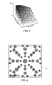
- FIG. 4 illustrates an image taken by the thickness measurement tool, shown in FIG. 3 ;
- FIG. 5 is simplified three dimensional representation of the image, shown in FIG. 4 ;
- FIG. 6 is a top down view of the substrate having a drop pattern positioned thereon;
- FIGS. 7A-7D illustrate exemplary steps for addressing a non-uniform residual layer
- FIG. 8 illustrates a process for compensating for a non-uniform residual layer.
- a system 8 to form a relief pattern on a substrate 12 includes a stage 10 upon which substrate 12 is supported and a template 14 , having a patterning surface 18 thereon.
- substrate 12 may be coupled to a substrate chuck (not shown), the substrate chuck (not shown) being any chuck including, but not limited to, vacuum and electromagnetic.
- Template 14 and/or mold 16 may be formed from such materials including but not limited to, fused-silica, quartz, silicon, organic polymers, siloxane polymers, borosilicate glass, fluorocarbon polymers, metal, and hardened sapphire.
- patterning surface 18 comprises features defined by a plurality of spaced-apart recesses 17 and protrusions 19 .
- patterning surface 18 may be substantially smooth and/or planar. Patterning surface 18 may define an original pattern that forms the basis of a pattern to be formed on substrate 12 .
- Template 14 may be coupled to an imprint head 20 to facilitate movement of template 14 , and therefore, mold 16 .
- template 14 may be coupled to a template chuck (not shown), the template chuck (not shown) being any chuck including, but not limited to, vacuum and electromagnetic.
- a fluid dispense system 22 is coupled to be selectively placed in fluid communication with substrate 12 so as to deposit polymeric material 24 thereon. It should be understood that polymeric material 24 may be deposited using any known technique, e.g., drop dispense, spin-coating, dip coating, chemical vapor deposition (CVD), physical vapor deposition (PVD), and the like.
- a source 26 of energy 28 is coupled to direct energy 28 along a path 30 .
- Imprint head 20 and stage 10 are configured to arrange mold 16 and substrate 12 , respectively, to be in superimposition and disposed in path 30 . Either imprint head 20 , stage 10 , or both vary a distance between mold 16 and substrate 12 to define a desired volume therebetween that is filled by polymeric material 24 .
- polymeric material 24 is disposed upon substrate 12 before the desired volume is defined between mold 16 and substrate 12 .
- polymeric material 24 may fill the volume after the desired volume has been obtained.
- source 26 produces energy 28 , e.g., broadband energy that causes polymeric material 24 to solidify and/or cross-link conforming to the shape of a surface 25 of substrate 12 and patterning surface 18 , defining a patterned layer 50 on substrate 12 having a contiguous formation of polymeric material 24 over surface 25 .
- patterned layer 50 comprises sub-portions 34 a and 34 b , with sub-portions 34 b being in superimposition with protrusions 19 , with sub-portions 34 a having a thickness t 1 and sub-portions 34 b having a thickness t 2 , with sub-portions 34 b commonly referred to as the residual layer.
- Thicknesses t 1 and t 2 may be any thickness desired, dependent upon the application.
- the broadband energy may comprise an actinic component including, but not limited to, ultraviolet wavelengths, thermal energy, electromagnetic energy, visible light and the like.
- the actinic component employed is known to one skilled in the art and typically depends on the material from which imprinting layer 12 is formed. Control of this process is regulated by a processor 32 that is in data communication with stage 10 , imprint head 20 , fluid dispense system 22 , source 26 , operating on a computer readable program stored in memory 34 .
- System 8 may further include a film thickness measurement tool 60 coupled with the substrate chuck (not shown), described further below. Film thickness measurement tool 60 may comprise an optical detection system, and further may be in data communication with processor 32 . Film thickness measurement tool 60 may be a stand alone tool commonly used in semiconductor fabrication. Such tools are commercially available from Metrosol, Inc., Filmetrics, Rudolph Technologies, and J.A. Woolam.
- Patterned layer 50 may have variations among thicknesses t 2 , which may be undesirable. More specifically, minimizing, if not preventing, variations among sub-portions 34 b , and thus, the residual layer may result in improved control of the critical dimension of pattered layer 50 , which may be desired. In an example, it may be desirable to reduce variations among sub-portions 34 b below the approximately 30 nm level seen in typical imprints in order to minimize, if not prevent, the impact to etched feature critical dimension.
- variations in thicknesses t 2 of sub-portions 34 b may be measured generating measured data, with the measured data facilitating a design in positioning of polymeric material 24 upon substrate 12 .
- polymeric material 24 is positioned as a plurality of droplets upon substrate 12 , and thus, the measured data facilitates a design in the drop pattern of polymeric material 24 .
- uniformity in thicknesses t 2 of the sub-portions 34 b may be achieved.
- the variations in thicknesses t 2 of sub-portions 34 b may be measured at a plurality of points employing film thickness measurement tool 60 , with the optical detection system digitizing imprinted fields, i.e., patterned layer 50 , and subsequently employing processor 32 operating on a computer readable program stored in memory 34 to analyze said imprinted fields to construct a map of the thickness t 2 of sub-portions 34 b across patterned layer 50 .
- the drop pattern of polymeric material 24 may be varied, i.e., droplets may be added or subtracted, the drop offset may be varied, individual drop volumes of the plurality of drops, based upon the variations in thickness t 2 of sub-portions 34 b to generate a drop pattern that may facilitate patterned layer 50 comprising sub-portions 34 b having a desired thickness uniformity.
- film thickness measurement tool 60 may be positioned at a fixed angle and distance from substrate 12 , with the distance from the imprint field, i.e., patterned layer 50 , to film thickness measurement tool 60 being calculated.
- a calibration process may be required to obtain accurate dimensions of the imprint field.
- An alternative method for measuring the residual layer thickness measures the optical properties of the film, such as reflected intensity versus wavelength or circular versus elliptical polarization of light reflected from the field. These spectroscopic measurements are then fit to a model of the film stack to determine parameters of interest such as film thickness. Such a process can be implemented using the commercially available film thickness measurement tools noted above.
- processor 32 operating on a computer readable program stored in memory 34 may employ an algorithm to convert the image into a square (or, rectangle, circular, etc.) imprint area. Subsequently, processor 32 may convert differences in color and shade grades into a Z-height profile of the imprint field.
- FIG. 5 shows an example of a three-dimensional representation of the field shown in FIG. 4 .
- the computer readable program stored in memory 34 may comprise a program entitled ImageJ available from http://rsb.info.nih.gov/ij/.
- the slope g(x,y) will be used to calculate the offsets in X and Y directions of the drop pattern.
- Deviation function w(x,y) will be used to control local unit fluid volume; number of drops, position of drops and drop volume itself.
- FIG. 6 shows an exemplary drop pattern of polymeric material 24 used for imprinting that produced a desired thickness profile shown on FIG. 5 .
- various drop patterns can be generated on the substrate, such as a uniform grid superimposed with localized compensating drops.
- the drop pattern on FIG. 6 corresponds to the following drop matrix, M(x,y):
- i and j are the unit vectors along X and Y axes.
- A, B are the proportionality coefficients that need to be determined experimentally, for instance, using a blank mesa template. Imprint new field and measure g(x,y) again. Verify that the slope in X and Y is near zero.
- M′(x,y) M ( x,y )* w ′( x,y )
- FIGS. 7A-7D and 8 A process for obtaining a uniform residual layer thickness (RLT) is illustrated in FIGS. 7A-7D and 8 .
- the imprint tool is calibrated to determine how much fluid to dispense to make an imprint with a desired thickness.
- a uniform distribution of fluid is deposited on the substrate as illustrated in FIG. 7A .
- An imprint is performed. Evaporation and other non-uniformities may cause the RLT to be non-uniform.
- RLT uniformity is measured across a dense array of points in the imprinted field using the film thickness measurement tool 60 .
- step 804 if a desired uniformity is achieved, then the process may end in step 805 . If not (see FIG.
- step 806 the process proceeds to step 806 , where one of the above algorithms is employed, such as in software running in processor 32 , to calculate a new corrected drop pattern, which will add drops, or increase drop size, to thin areas and/or remove drops, or decrease drop size, from thick areas to achieve improved RLT uniformity.
- the process then returns to step 802 to make a new imprint using the corrected drop pattern (see FIG. 7C ), and steps 803 and 804 are performed again. This process may be repeated as needed until a desired uniformity RLT is achieved, as illustrated in FIG. 7D .
- This above-mentioned method may be employed to obtain a desired volume of polymeric fluid 24 positioned upon substrate 12 to the volume of features (protrusions 17 and recesses 19 ) in mold 16 .
- the above-mentioned method may be employed to compensate for evaporation in the plurality of droplets of polymeric material 24 after positioning the same upon substrate 12 and prior to contact with mold 16 .
- matching a volume of polymeric material 24 upon substrate 12 to the volume of features in mold 16 result in improved residual layer uniformity, i.e., variations among thicknesses t 2 of sub-portions 34 b .
- This improved residual layer uniformity enables better control of feature CDs across imprinted and etched wafers.
- the above-mentioned may also minimize, if not reduce, and impact of faceting during a breakthrough etch of the residual layer.
Abstract
Description
-
- (0,0) refers to the center of the template
S=−A grad(g(x,y))i−B grad(g(x,y))j,
w′(x,y)=w(x,y)/(max(w(x,y))−min(w(x,y)))
M′(x,y)=M(x,y)*w′(x,y)
Claims (20)
Priority Applications (1)
| Application Number | Priority Date | Filing Date | Title |
|---|---|---|---|
| US12/835,009 US8647554B2 (en) | 2004-06-15 | 2010-07-13 | Residual layer thickness measurement and correction |
Applications Claiming Priority (5)
| Application Number | Priority Date | Filing Date | Title |
|---|---|---|---|
| US57987804P | 2004-06-15 | 2004-06-15 | |
| US11/143,092 US20050270312A1 (en) | 2004-06-03 | 2005-06-02 | Fluid dispensing and drop-on-demand dispensing for nano-scale manufacturing |
| US78880806P | 2006-04-03 | 2006-04-03 | |
| US11/694,017 US20070228593A1 (en) | 2006-04-03 | 2007-03-30 | Residual Layer Thickness Measurement and Correction |
| US12/835,009 US8647554B2 (en) | 2004-06-15 | 2010-07-13 | Residual layer thickness measurement and correction |
Related Parent Applications (1)
| Application Number | Title | Priority Date | Filing Date |
|---|---|---|---|
| US11/694,017 Continuation US20070228593A1 (en) | 2004-06-15 | 2007-03-30 | Residual Layer Thickness Measurement and Correction |
Publications (2)
| Publication Number | Publication Date |
|---|---|
| US20100286811A1 US20100286811A1 (en) | 2010-11-11 |
| US8647554B2 true US8647554B2 (en) | 2014-02-11 |
Family
ID=39468401
Family Applications (2)
| Application Number | Title | Priority Date | Filing Date |
|---|---|---|---|
| US11/694,017 Abandoned US20070228593A1 (en) | 2004-06-15 | 2007-03-30 | Residual Layer Thickness Measurement and Correction |
| US12/835,009 Active 2027-06-14 US8647554B2 (en) | 2004-06-15 | 2010-07-13 | Residual layer thickness measurement and correction |
Family Applications Before (1)
| Application Number | Title | Priority Date | Filing Date |
|---|---|---|---|
| US11/694,017 Abandoned US20070228593A1 (en) | 2004-06-15 | 2007-03-30 | Residual Layer Thickness Measurement and Correction |
Country Status (3)
| Country | Link |
|---|---|
| US (2) | US20070228593A1 (en) |
| TW (1) | TWI360835B (en) |
| WO (1) | WO2008066562A2 (en) |
Cited By (5)
| Publication number | Priority date | Publication date | Assignee | Title |
|---|---|---|---|---|
| US9811671B1 (en) | 2000-05-24 | 2017-11-07 | Copilot Ventures Fund Iii Llc | Authentication method and system |
| US9846814B1 (en) | 2008-04-23 | 2017-12-19 | Copilot Ventures Fund Iii Llc | Authentication method and system |
| US9993962B2 (en) * | 2016-05-23 | 2018-06-12 | Canon Kabushiki Kaisha | Method of imprinting to correct for a distortion within an imprint system |
| US10150231B2 (en) | 2012-04-27 | 2018-12-11 | Canon Kabushiki Kaisha | Method for manufacturing photo cured material |
| US11927883B2 (en) | 2018-03-30 | 2024-03-12 | Canon Kabushiki Kaisha | Method and apparatus to reduce variation of physical attribute of droplets using performance characteristic of dispensers |
Families Citing this family (42)
| Publication number | Priority date | Publication date | Assignee | Title |
|---|---|---|---|---|
| US7019819B2 (en) | 2002-11-13 | 2006-03-28 | Molecular Imprints, Inc. | Chucking system for modulating shapes of substrates |
| US7442336B2 (en) * | 2003-08-21 | 2008-10-28 | Molecular Imprints, Inc. | Capillary imprinting technique |
| US8211214B2 (en) | 2003-10-02 | 2012-07-03 | Molecular Imprints, Inc. | Single phase fluid imprint lithography method |
| US20060062922A1 (en) | 2004-09-23 | 2006-03-23 | Molecular Imprints, Inc. | Polymerization technique to attenuate oxygen inhibition of solidification of liquids and composition therefor |
| MY144847A (en) | 2005-12-08 | 2011-11-30 | Molecular Imprints Inc | Method and system for double-sided patterning of substrates |
| US7670530B2 (en) | 2006-01-20 | 2010-03-02 | Molecular Imprints, Inc. | Patterning substrates employing multiple chucks |
| US8142850B2 (en) * | 2006-04-03 | 2012-03-27 | Molecular Imprints, Inc. | Patterning a plurality of fields on a substrate to compensate for differing evaporation times |
| WO2007124007A2 (en) * | 2006-04-21 | 2007-11-01 | Molecular Imprints, Inc. | Method for detecting a particle in a nanoimprint lithography system |
| US8215946B2 (en) | 2006-05-18 | 2012-07-10 | Molecular Imprints, Inc. | Imprint lithography system and method |
| US20090014917A1 (en) * | 2007-07-10 | 2009-01-15 | Molecular Imprints, Inc. | Drop Pattern Generation for Imprint Lithography |
| JP4908369B2 (en) * | 2007-10-02 | 2012-04-04 | 株式会社東芝 | Imprint method and imprint system |
| US8119052B2 (en) * | 2007-11-02 | 2012-02-21 | Molecular Imprints, Inc. | Drop pattern generation for imprint lithography |
| US20090148619A1 (en) * | 2007-12-05 | 2009-06-11 | Molecular Imprints, Inc. | Controlling Thickness of Residual Layer |
| WO2009078881A1 (en) * | 2007-12-19 | 2009-06-25 | Hewlett-Packard Development Company, L.P. | Imprint lithography apparatus and method |
| US8361371B2 (en) * | 2008-02-08 | 2013-01-29 | Molecular Imprints, Inc. | Extrusion reduction in imprint lithography |
| TWI423306B (en) * | 2008-06-09 | 2014-01-11 | Univ Texas | Adaptive nanotopography sculpting |
| JP5349588B2 (en) * | 2008-06-09 | 2013-11-20 | ボード・オブ・リージエンツ,ザ・ユニバーシテイ・オブ・テキサス・システム | Adaptive nanotopography sculpting |
| JP2010076219A (en) * | 2008-09-25 | 2010-04-08 | Canon Inc | Method for processing substrate by nanoimprint |
| US8512797B2 (en) | 2008-10-21 | 2013-08-20 | Molecular Imprints, Inc. | Drop pattern generation with edge weighting |
| US8586126B2 (en) | 2008-10-21 | 2013-11-19 | Molecular Imprints, Inc. | Robust optimization to generate drop patterns in imprint lithography which are tolerant of variations in drop volume and drop placement |
| US20100101493A1 (en) * | 2008-10-27 | 2010-04-29 | Molecular Imprints, Inc. | Dispense System |
| US20100104747A1 (en) * | 2008-10-28 | 2010-04-29 | Molecular Imprints, Inc. | Drop Deposition Control |
| US20100112220A1 (en) * | 2008-11-03 | 2010-05-06 | Molecular Imprints, Inc. | Dispense system set-up and characterization |
| JP4892026B2 (en) * | 2009-03-19 | 2012-03-07 | 株式会社東芝 | Pattern formation method |
| JP5238742B2 (en) * | 2010-03-19 | 2013-07-17 | 株式会社東芝 | Processing method and processing apparatus |
| JP5460541B2 (en) * | 2010-03-30 | 2014-04-02 | 富士フイルム株式会社 | Nanoimprint method, droplet arrangement pattern creation method, and substrate processing method |
| JP5744422B2 (en) | 2010-06-17 | 2015-07-08 | キヤノン株式会社 | Imprint method, imprint apparatus, sample shot extraction method, and article manufacturing method using the same |
| JP5337776B2 (en) | 2010-09-24 | 2013-11-06 | 富士フイルム株式会社 | Nanoimprint method and substrate processing method using the same |
| JP5595949B2 (en) | 2011-02-15 | 2014-09-24 | 株式会社東芝 | Imprint apparatus, imprint method, and method of manufacturing uneven plate |
| JP2012181166A (en) * | 2011-03-03 | 2012-09-20 | Dainippon Screen Mfg Co Ltd | Film shape acquisition device and film shape acquisition method |
| JP5611912B2 (en) | 2011-09-01 | 2014-10-22 | 株式会社東芝 | Imprint resist material, pattern forming method, and imprint apparatus |
| US9623623B2 (en) | 2012-08-24 | 2017-04-18 | Hewlett-Packard Indigo B.V. | Thickness calibration of an embossing die |
| JP6395352B2 (en) * | 2013-07-12 | 2018-09-26 | キヤノン株式会社 | Imprint apparatus, imprint method, and article manufacturing method using the same |
| JP2015088667A (en) * | 2013-10-31 | 2015-05-07 | 株式会社東芝 | Microfabrication system, microfabrication device, and microfabrication method |
| JP6262015B2 (en) * | 2014-02-17 | 2018-01-17 | 東芝メモリ株式会社 | Resist placement method and resist placement program |
| US10120276B2 (en) * | 2015-03-31 | 2018-11-06 | Canon Kabushiki Kaisha | Imprint apparatus, imprint method, and method of manufacturing article |
| JP6602033B2 (en) * | 2015-03-31 | 2019-11-06 | キヤノン株式会社 | Imprint apparatus, supply amount distribution generation method, imprint method, and article manufacturing method |
| JP6611450B2 (en) * | 2015-03-31 | 2019-11-27 | キヤノン株式会社 | Imprint apparatus, imprint method, and article manufacturing method |
| JP6742177B2 (en) * | 2016-07-15 | 2020-08-19 | キヤノン株式会社 | Imprint apparatus and article manufacturing method |
| US11036130B2 (en) * | 2017-10-19 | 2021-06-15 | Canon Kabushiki Kaisha | Drop placement evaluation |
| KR102527567B1 (en) * | 2018-02-23 | 2023-05-03 | 에스케이하이닉스 주식회사 | Method of forming imprinted patterns for suppressing template damages from particles |
| US10725375B2 (en) | 2018-12-04 | 2020-07-28 | Canon Kabushiki Kaisha | Using non-linear fluid dispensers for forming thick films |
Citations (125)
| Publication number | Priority date | Publication date | Assignee | Title |
|---|---|---|---|---|
| US1236304A (en) | 1917-02-03 | 1917-08-07 | Riley L Howell | Cushioned hand-stamp. |
| US3503538A (en) | 1966-11-29 | 1970-03-31 | Bp Chem Int Ltd | Metering process and apparatus |
| US3781214A (en) | 1970-11-25 | 1973-12-25 | Dainippon Ink & Chemicals | Photopolymerizable printing ink |
| US4512848A (en) | 1984-02-06 | 1985-04-23 | Exxon Research And Engineering Co. | Procedure for fabrication of microstructures over large areas using physical replication |
| US4731155A (en) | 1987-04-15 | 1988-03-15 | General Electric Company | Process for forming a lithographic mask |
| US4848911A (en) | 1986-06-11 | 1989-07-18 | Kabushiki Kaisha Toshiba | Method for aligning first and second objects, relative to each other, and apparatus for practicing this method |
| US4936465A (en) | 1987-12-07 | 1990-06-26 | Zoeld Tibor | Method and apparatus for fast, reliable, and environmentally safe dispensing of fluids, gases and individual particles of a suspension through pressure control at well defined parts of a closed flow-through system |
| US4959252A (en) | 1986-09-29 | 1990-09-25 | Rhone-Poulenc Chimie | Highly oriented thermotropic optical disc member |
| US5028366A (en) | 1988-01-12 | 1991-07-02 | Air Products And Chemicals, Inc. | Water based mold release compositions for making molded polyurethane foam |
| US5110514A (en) | 1989-05-01 | 1992-05-05 | Soane Technologies, Inc. | Controlled casting of a shrinkable material |
| US5148037A (en) | 1988-09-09 | 1992-09-15 | Canon Kabushiki Kaisha | Position detecting method and apparatus |
| US5151754A (en) | 1989-10-06 | 1992-09-29 | Kabushiki Kaisha Toshiba | Method and an apparatus for measuring a displacement between two objects and a method and an apparatus for measuring a gap distance between two objects |
| US5240550A (en) | 1990-09-21 | 1993-08-31 | U.S. Philips Corp. | Method of forming at least one groove in a substrate layer |
| US5259926A (en) | 1991-09-24 | 1993-11-09 | Hitachi, Ltd. | Method of manufacturing a thin-film pattern on a substrate |
| US5362940A (en) | 1990-11-09 | 1994-11-08 | Litel Instruments | Use of Fresnel zone plates for material processing |
| US5371822A (en) | 1992-06-09 | 1994-12-06 | Digital Equipment Corporation | Method of packaging and assembling opto-electronic integrated circuits |
| US5425848A (en) | 1993-03-16 | 1995-06-20 | U.S. Philips Corporation | Method of providing a patterned relief of cured photoresist on a flat substrate surface and device for carrying out such a method |
| US5445195A (en) | 1992-07-15 | 1995-08-29 | Kim; Dae S. | Automatic computer-controlled liquid dispenser |
| US5449117A (en) | 1993-10-04 | 1995-09-12 | Technical Concepts, L.P. | Apparatus and method for controllably dispensing drops of liquid |
| US5480047A (en) | 1993-06-04 | 1996-01-02 | Sharp Kabushiki Kaisha | Method for forming a fine resist pattern |
| US5512131A (en) | 1993-10-04 | 1996-04-30 | President And Fellows Of Harvard College | Formation of microstamped patterns on surfaces and derivative articles |
| US5542605A (en) | 1994-04-07 | 1996-08-06 | Flow-Rite Controls, Ltd. | Automatic liquid dispenser |
| US5545367A (en) | 1992-04-15 | 1996-08-13 | Soane Technologies, Inc. | Rapid prototype three dimensional stereolithography |
| US5601641A (en) | 1992-07-21 | 1997-02-11 | Tse Industries, Inc. | Mold release composition with polybutadiene and method of coating a mold core |
| US5669303A (en) | 1996-03-04 | 1997-09-23 | Motorola | Apparatus and method for stamping a surface |
| US5723176A (en) | 1994-03-02 | 1998-03-03 | Telecommunications Research Laboratories | Method and apparatus for making optical components by direct dispensing of curable liquid |
| US5747102A (en) | 1995-11-16 | 1998-05-05 | Nordson Corporation | Method and apparatus for dispensing small amounts of liquid material |
| US5772905A (en) | 1995-11-15 | 1998-06-30 | Regents Of The University Of Minnesota | Nanoimprint lithography |
| US5776748A (en) | 1993-10-04 | 1998-07-07 | President And Fellows Of Harvard College | Method of formation of microstamped patterns on plates for adhesion of cells and other biological materials, devices and uses therefor |
| US5812629A (en) | 1997-04-30 | 1998-09-22 | Clauser; John F. | Ultrahigh resolution interferometric x-ray imaging |
| US5820769A (en) | 1995-05-24 | 1998-10-13 | Regents Of The University Of Minnesota | Method for making magnetic storage having discrete elements with quantized magnetic moments |
| US5849222A (en) | 1995-09-29 | 1998-12-15 | Johnson & Johnson Vision Products, Inc. | Method for reducing lens hole defects in production of contact lens blanks |
| US5849209A (en) | 1995-03-31 | 1998-12-15 | Johnson & Johnson Vision Products, Inc. | Mold material made with additives |
| US5858580A (en) | 1997-09-17 | 1999-01-12 | Numerical Technologies, Inc. | Phase shifting circuit manufacture method and apparatus |
| US5886650A (en) | 1996-10-31 | 1999-03-23 | Mitsumi Electric Co., Ltd. | Car navigation system with FM multi-broadcast signal receiving function |
| US5948470A (en) | 1997-04-28 | 1999-09-07 | Harrison; Christopher | Method of nanoscale patterning and products made thereby |
| US5974150A (en) | 1997-09-30 | 1999-10-26 | Tracer Detection Technology Corp. | System and method for authentication of goods |
| US6027595A (en) | 1998-07-02 | 2000-02-22 | Samsung Electronics Co., Ltd. | Method of making optical replicas by stamping in photoresist and replicas formed thereby |
| US6046056A (en) | 1996-06-28 | 2000-04-04 | Caliper Technologies Corporation | High throughput screening assay systems in microscale fluidic devices |
| US6048623A (en) | 1996-12-18 | 2000-04-11 | Kimberly-Clark Worldwide, Inc. | Method of contact printing on gold coated films |
| US6074827A (en) | 1996-07-30 | 2000-06-13 | Aclara Biosciences, Inc. | Microfluidic method for nucleic acid purification and processing |
| US6089853A (en) | 1997-12-24 | 2000-07-18 | International Business Machines Corporation | Patterning device for patterning a substrate with patterning cavities fed by service cavities |
| US6218316B1 (en) | 1998-10-22 | 2001-04-17 | Micron Technology, Inc. | Planarization of non-planar surfaces in device fabrication |
| US6274294B1 (en) | 1999-02-03 | 2001-08-14 | Electroformed Stents, Inc. | Cylindrical photolithography exposure process and apparatus |
| US6279474B1 (en) | 1993-08-13 | 2001-08-28 | Heidelberger Druckmaschinen Ag | Method and device for transferring ink in a printing unit of an offset printing press |
| US6306467B1 (en) | 1999-06-14 | 2001-10-23 | Ford Global Technologies, Inc. | Method of solid free form fabrication of objects |
| US6309580B1 (en) | 1995-11-15 | 2001-10-30 | Regents Of The University Of Minnesota | Release surfaces, particularly for use in nanoimprint lithography |
| US6326627B1 (en) | 2000-08-02 | 2001-12-04 | Archimedes Technology Group, Inc. | Mass filtering sputtered ion source |
| US6334960B1 (en) | 1999-03-11 | 2002-01-01 | Board Of Regents, The University Of Texas System | Step and flash imprint lithography |
| US20020005880A1 (en) | 1996-04-23 | 2002-01-17 | Xaar Technology Limited | Droplet deposition apparatus |
| US6348999B1 (en) | 1995-05-10 | 2002-02-19 | Epigem Limited | Micro relief element and preparation thereof |
| US6355198B1 (en) | 1996-03-15 | 2002-03-12 | President And Fellows Of Harvard College | Method of forming articles including waveguides via capillary micromolding and microtransfer molding |
| US20020042027A1 (en) | 1998-10-09 | 2002-04-11 | Chou Stephen Y. | Microscale patterning and articles formed thereby |
| US6387330B1 (en) | 2000-04-12 | 2002-05-14 | George Steven Bova | Method and apparatus for storing and dispensing reagents |
| US6391217B2 (en) | 1999-12-23 | 2002-05-21 | University Of Massachusetts | Methods and apparatus for forming submicron patterns on films |
| US20020094496A1 (en) | 2000-07-17 | 2002-07-18 | Choi Byung J. | Method and system of automatic fluid dispensing for imprint lithography processes |
| US20020122873A1 (en) | 2000-01-05 | 2002-09-05 | Mirkin Chad A. | Nanolithography methods and products therefor and produced thereby |
| US20020132482A1 (en) | 2000-07-18 | 2002-09-19 | Chou Stephen Y. | Fluid pressure imprint lithography |
| US20020135099A1 (en) | 2001-01-19 | 2002-09-26 | Robinson Timothy R. | Mold with metal oxide surface compatible with ionic release agents |
| EP1254704A2 (en) | 2001-04-30 | 2002-11-06 | Agilent Technologies Inc | Error detection in a chemical array fabrication |
| US20020168578A1 (en) | 1996-09-18 | 2002-11-14 | Numerical Technologies, Inc. | Phase shifting circuit manufacture method and apparatus |
| US20020170880A1 (en) | 2001-03-22 | 2002-11-21 | Yong Chen | Scanning probe based lithographic alignment |
| US6498640B1 (en) | 1999-12-30 | 2002-12-24 | Koninklijke Philips Electronics N.V. | Method to measure alignment using latent image grating structures |
| US20030001992A1 (en) | 2001-06-29 | 2003-01-02 | Seiko Epson Corporation | Color filter substrate, method for manufacturing color filter substrates, liquid crystal display device, electro-optical device, method of manufacturing electro-optical device, and electronic apparatus |
| US20030025895A1 (en) | 2001-08-03 | 2003-02-06 | Michael Binnard | Apparatus and methods for detecting tool-induced shift in microlithography apparatus |
| US6517977B2 (en) | 2001-03-28 | 2003-02-11 | Motorola, Inc. | Lithographic template and method of formation and use |
| US6517995B1 (en) | 1999-09-14 | 2003-02-11 | Massachusetts Institute Of Technology | Fabrication of finely featured devices by liquid embossing |
| US6518189B1 (en) | 1995-11-15 | 2003-02-11 | Regents Of The University Of Minnesota | Method and apparatus for high density nanostructures |
| US20030062334A1 (en) | 2001-09-25 | 2003-04-03 | Lee Hong Hie | Method for forming a micro-pattern on a substrate by using capillary force |
| US20030080471A1 (en) | 2001-10-29 | 2003-05-01 | Chou Stephen Y. | Lithographic method for molding pattern with nanoscale features |
| US20030081193A1 (en) | 2001-06-01 | 2003-05-01 | White Donald L. | Holder, system, and process for improving overlay in lithography |
| US6580172B2 (en) | 2001-03-02 | 2003-06-17 | Motorola, Inc. | Lithographic template and method of formation and use |
| US20030137494A1 (en) | 2000-05-01 | 2003-07-24 | Tulbert David J. | Human-machine interface |
| US6621960B2 (en) | 2002-01-24 | 2003-09-16 | Oplink Communications, Inc. | Method of fabricating multiple superimposed fiber Bragg gratings |
| US20030174435A1 (en) | 2002-03-18 | 2003-09-18 | International Business Machines Corporation | Method and apparatus for providing an aligned coil for an inductive head structure using a patterned seed layer |
| US6623579B1 (en) | 1999-11-02 | 2003-09-23 | Alien Technology Corporation | Methods and apparatus for fluidic self assembly |
| US20030186140A1 (en) | 2001-06-27 | 2003-10-02 | Fries David P. | Maskless photolithography for using photoreactive agents |
| US6646662B1 (en) | 1998-05-26 | 2003-11-11 | Seiko Epson Corporation | Patterning method, patterning apparatus, patterning template, and method for manufacturing the patterning template |
| US20040029041A1 (en) | 2002-02-27 | 2004-02-12 | Brewer Science, Inc. | Novel planarization method for multi-layer lithography processing |
| US6696220B2 (en) | 2000-10-12 | 2004-02-24 | Board Of Regents, The University Of Texas System | Template for room temperature, low pressure micro-and nano-imprint lithography |
| US20040036201A1 (en) | 2000-07-18 | 2004-02-26 | Princeton University | Methods and apparatus of field-induced pressure imprint lithography |
| US20040046288A1 (en) | 2000-07-18 | 2004-03-11 | Chou Stephen Y. | Laset assisted direct imprint lithography |
| US20040058067A1 (en) | 2002-09-19 | 2004-03-25 | Law Kam S. | Method and apparatus for metallization of large area substrates |
| US20040065976A1 (en) | 2002-10-04 | 2004-04-08 | Sreenivasan Sidlgata V. | Method and a mold to arrange features on a substrate to replicate features having minimal dimensional variability |
| US20040110856A1 (en) | 2002-12-04 | 2004-06-10 | Young Jung Gun | Polymer solution for nanoimprint lithography to reduce imprint temperature and pressure |
| US20040131718A1 (en) | 2000-07-18 | 2004-07-08 | Princeton University | Lithographic apparatus for fluid pressure imprint lithography |
| US20040137734A1 (en) | 1995-11-15 | 2004-07-15 | Princeton University | Compositions and processes for nanoimprinting |
| US20040156108A1 (en) | 2001-10-29 | 2004-08-12 | Chou Stephen Y. | Articles comprising nanoscale patterns with reduced edge roughness and methods of making same |
| US6776094B1 (en) | 1993-10-04 | 2004-08-17 | President & Fellows Of Harvard College | Kit For Microcontact Printing |
| US20040192041A1 (en) | 2003-03-27 | 2004-09-30 | Jun-Ho Jeong | UV nanoimprint lithography process using elementwise embossed stamp and selectively additive pressurization |
| US20040197843A1 (en) | 2001-07-25 | 2004-10-07 | Chou Stephen Y. | Nanochannel arrays and their preparation and use for high throughput macromolecular analysis |
| US20040231781A1 (en) | 2003-05-23 | 2004-11-25 | Agency For Science, Technology And Research | Methods of creating patterns on substrates and articles of manufacture resulting therefrom |
| US20040250945A1 (en) | 2003-06-10 | 2004-12-16 | Industrial Technology Research Institute | Method for and apparatus for bonding patterned imprint to a substrate by adhering means |
| US20040261703A1 (en) | 2003-06-27 | 2004-12-30 | Jeffrey D. Chinn | Apparatus and method for controlled application of reactive vapors to produce thin films and coatings |
| US6849558B2 (en) | 2002-05-22 | 2005-02-01 | The Board Of Trustees Of The Leland Stanford Junior University | Replication and transfer of microstructures and nanostructures |
| US6855293B1 (en) | 1999-03-23 | 2005-02-15 | Hahn-Schickard-Gesellschaft Fuer Angewandte Forschung E.V. | Fluids manipulation device with format conversion |
| US20050037143A1 (en) | 2000-07-18 | 2005-02-17 | Chou Stephen Y. | Imprint lithography with improved monitoring and control and apparatus therefor |
| US6873087B1 (en) | 1999-10-29 | 2005-03-29 | Board Of Regents, The University Of Texas System | High precision orientation alignment and gap control stages for imprint lithography processes |
| US6879162B2 (en) | 2000-11-07 | 2005-04-12 | Sri International | System and method of micro-fluidic handling and dispensing using micro-nozzle structures |
| US20050106321A1 (en) | 2003-11-14 | 2005-05-19 | Molecular Imprints, Inc. | Dispense geometery to achieve high-speed filling and throughput |
| US6900881B2 (en) | 2002-07-11 | 2005-05-31 | Molecular Imprints, Inc. | Step and repeat imprint lithography systems |
| US6908861B2 (en) | 2002-07-11 | 2005-06-21 | Molecular Imprints, Inc. | Method for imprint lithography using an electric field |
| US20050145119A1 (en) | 2000-07-18 | 2005-07-07 | Hua Tan | Apparatus for fluid pressure imprint lithography |
| US6916585B2 (en) | 2000-07-16 | 2005-07-12 | Board Of Regents, The University Of Texas Systems | Method of varying template dimensions to achieve alignment during imprint lithography |
| US6916584B2 (en) | 2002-08-01 | 2005-07-12 | Molecular Imprints, Inc. | Alignment methods for imprint lithography |
| US20050160011A1 (en) | 2004-01-20 | 2005-07-21 | Molecular Imprints, Inc. | Method for concurrently employing differing materials to form a layer on a substrate |
| US20050156357A1 (en) | 2002-12-12 | 2005-07-21 | Board Of Regents, The University Of Texas System | Planarization method of patterning a substrate |
| US20050156353A1 (en) | 2004-01-15 | 2005-07-21 | Watts Michael P. | Method to improve the flow rate of imprinting material |
| US20050170670A1 (en) | 2003-11-17 | 2005-08-04 | King William P. | Patterning of sacrificial materials |
| US20050176242A1 (en) | 2002-07-26 | 2005-08-11 | Seiko Epson Corporation | Patterning method |
| US6932934B2 (en) | 2002-07-11 | 2005-08-23 | Molecular Imprints, Inc. | Formation of discontinuous films during an imprint lithography process |
| US6936194B2 (en) | 2002-09-05 | 2005-08-30 | Molecular Imprints, Inc. | Functional patterning material for imprint lithography processes |
| US20050189676A1 (en) | 2004-02-27 | 2005-09-01 | Molecular Imprints, Inc. | Full-wafer or large area imprinting with multiple separated sub-fields for high throughput lithography |
| US20050230882A1 (en) | 2004-04-19 | 2005-10-20 | Molecular Imprints, Inc. | Method of forming a deep-featured template employed in imprint lithography |
| US6964793B2 (en) | 2002-05-16 | 2005-11-15 | Board Of Regents, The University Of Texas System | Method for fabricating nanoscale patterns in light curable compositions using an electric field |
| US20050253307A1 (en) | 2004-05-11 | 2005-11-17 | Molecualr Imprints, Inc. | Method of patterning a conductive layer on a substrate |
| US20050253137A1 (en) | 2003-11-20 | 2005-11-17 | President And Fellows Of Harvard College | Nanoscale arrays, robust nanostructures, and related devices |
| US20050276919A1 (en) | 2004-06-01 | 2005-12-15 | Molecular Imprints, Inc. | Method for dispensing a fluid on a substrate |
| US20050284886A1 (en) | 2004-06-25 | 2005-12-29 | Cristian Penciu | Apparatus for mixing and dispensing fluids |
| US20060076717A1 (en) | 2002-07-11 | 2006-04-13 | Molecular Imprints, Inc. | Step and repeat imprint lithography processes |
| US20060121728A1 (en) | 2004-12-07 | 2006-06-08 | Molecular Imprints, Inc. | Method for fast filling of templates for imprint lithography using on template dispense |
| US20060213441A1 (en) | 2003-06-27 | 2006-09-28 | Applied Microstructures, Inc. | Apparatus and method for controlled application of reactive vapors to produce thin films and coatings |
| US7122482B2 (en) | 2003-10-27 | 2006-10-17 | Molecular Imprints, Inc. | Methods for fabricating patterned features utilizing imprint lithography |
| US7128875B2 (en) | 1995-04-10 | 2006-10-31 | Cubicciotti Roger S | Signal processing devices comprising biological and bio-mimetic components |
| US20060279024A1 (en) | 2003-06-17 | 2006-12-14 | Molecular Imprints, Inc. | Method for providing desirable wetting and release characteristics between a mold and a polymerizable composition |
Family Cites Families (13)
| Publication number | Priority date | Publication date | Assignee | Title |
|---|---|---|---|---|
| US4731156A (en) * | 1987-02-25 | 1988-03-15 | Itt Avionics, A Division Of Itt Corporation | Plasma processes for surface modification of fluoropolymers using ammonia |
| JP2560362B2 (en) * | 1987-12-18 | 1996-12-04 | 富士通株式会社 | Multiple reflector |
| JP3197010B2 (en) * | 1990-03-05 | 2001-08-13 | 株式会社東芝 | Interval setting method and interval setting device |
| US5317386A (en) * | 1991-09-06 | 1994-05-31 | Eastman Kodak Company | Optical monitor for measuring a gap between two rollers |
| US5888650A (en) * | 1996-06-03 | 1999-03-30 | Minnesota Mining And Manufacturing Company | Temperature-responsive adhesive article |
| DE19741655A1 (en) * | 1997-03-12 | 1999-03-25 | Ascom Frako Gmbh | Circuit for continuously variable direct or indirect variation of the direct current and / or alternating current flowing through a consumer operated by a direct or alternating voltage or any combination thereof |
| JP3939048B2 (en) * | 1999-05-17 | 2007-06-27 | セイコーインスツル株式会社 | Piezoelectric actuator |
| TW519593B (en) * | 2000-06-20 | 2003-02-01 | Fatwire Corp | System and method for least work publishing |
| US7027156B2 (en) * | 2002-08-01 | 2006-04-11 | Molecular Imprints, Inc. | Scatterometry alignment for imprint lithography |
| US6846360B2 (en) * | 2003-01-13 | 2005-01-25 | Aptos Corporation | Apparatus and method for bubble-free application of a resin to a substrate |
| US7019835B2 (en) * | 2004-02-19 | 2006-03-28 | Molecular Imprints, Inc. | Method and system to measure characteristics of a film disposed on a substrate |
| KR101193918B1 (en) * | 2004-06-03 | 2012-10-29 | 몰레큘러 임프린츠 인코퍼레이티드 | Fluid dispensing and drop-on-demand dispensing for nano-scale menufacturing |
| US7360851B1 (en) * | 2006-02-15 | 2008-04-22 | Kla-Tencor Technologies Corporation | Automated pattern recognition of imprint technology |
-
2007
- 2007-03-30 US US11/694,017 patent/US20070228593A1/en not_active Abandoned
- 2007-04-03 TW TW096111821A patent/TWI360835B/en active
- 2007-04-03 WO PCT/US2007/008424 patent/WO2008066562A2/en active Application Filing
-
2010
- 2010-07-13 US US12/835,009 patent/US8647554B2/en active Active
Patent Citations (144)
| Publication number | Priority date | Publication date | Assignee | Title |
|---|---|---|---|---|
| US1236304A (en) | 1917-02-03 | 1917-08-07 | Riley L Howell | Cushioned hand-stamp. |
| US3503538A (en) | 1966-11-29 | 1970-03-31 | Bp Chem Int Ltd | Metering process and apparatus |
| US3781214A (en) | 1970-11-25 | 1973-12-25 | Dainippon Ink & Chemicals | Photopolymerizable printing ink |
| US4512848A (en) | 1984-02-06 | 1985-04-23 | Exxon Research And Engineering Co. | Procedure for fabrication of microstructures over large areas using physical replication |
| US4848911A (en) | 1986-06-11 | 1989-07-18 | Kabushiki Kaisha Toshiba | Method for aligning first and second objects, relative to each other, and apparatus for practicing this method |
| US4959252A (en) | 1986-09-29 | 1990-09-25 | Rhone-Poulenc Chimie | Highly oriented thermotropic optical disc member |
| US4731155A (en) | 1987-04-15 | 1988-03-15 | General Electric Company | Process for forming a lithographic mask |
| US4936465A (en) | 1987-12-07 | 1990-06-26 | Zoeld Tibor | Method and apparatus for fast, reliable, and environmentally safe dispensing of fluids, gases and individual particles of a suspension through pressure control at well defined parts of a closed flow-through system |
| US5028366A (en) | 1988-01-12 | 1991-07-02 | Air Products And Chemicals, Inc. | Water based mold release compositions for making molded polyurethane foam |
| US5148037A (en) | 1988-09-09 | 1992-09-15 | Canon Kabushiki Kaisha | Position detecting method and apparatus |
| US5110514A (en) | 1989-05-01 | 1992-05-05 | Soane Technologies, Inc. | Controlled casting of a shrinkable material |
| US5151754A (en) | 1989-10-06 | 1992-09-29 | Kabushiki Kaisha Toshiba | Method and an apparatus for measuring a displacement between two objects and a method and an apparatus for measuring a gap distance between two objects |
| US5240550A (en) | 1990-09-21 | 1993-08-31 | U.S. Philips Corp. | Method of forming at least one groove in a substrate layer |
| US5362940A (en) | 1990-11-09 | 1994-11-08 | Litel Instruments | Use of Fresnel zone plates for material processing |
| US5259926A (en) | 1991-09-24 | 1993-11-09 | Hitachi, Ltd. | Method of manufacturing a thin-film pattern on a substrate |
| US5545367A (en) | 1992-04-15 | 1996-08-13 | Soane Technologies, Inc. | Rapid prototype three dimensional stereolithography |
| US5371822A (en) | 1992-06-09 | 1994-12-06 | Digital Equipment Corporation | Method of packaging and assembling opto-electronic integrated circuits |
| US5445195A (en) | 1992-07-15 | 1995-08-29 | Kim; Dae S. | Automatic computer-controlled liquid dispenser |
| US5601641A (en) | 1992-07-21 | 1997-02-11 | Tse Industries, Inc. | Mold release composition with polybutadiene and method of coating a mold core |
| US5425848A (en) | 1993-03-16 | 1995-06-20 | U.S. Philips Corporation | Method of providing a patterned relief of cured photoresist on a flat substrate surface and device for carrying out such a method |
| US5480047A (en) | 1993-06-04 | 1996-01-02 | Sharp Kabushiki Kaisha | Method for forming a fine resist pattern |
| US6279474B1 (en) | 1993-08-13 | 2001-08-28 | Heidelberger Druckmaschinen Ag | Method and device for transferring ink in a printing unit of an offset printing press |
| US5449117A (en) | 1993-10-04 | 1995-09-12 | Technical Concepts, L.P. | Apparatus and method for controllably dispensing drops of liquid |
| US5512131A (en) | 1993-10-04 | 1996-04-30 | President And Fellows Of Harvard College | Formation of microstamped patterns on surfaces and derivative articles |
| US5776748A (en) | 1993-10-04 | 1998-07-07 | President And Fellows Of Harvard College | Method of formation of microstamped patterns on plates for adhesion of cells and other biological materials, devices and uses therefor |
| US6776094B1 (en) | 1993-10-04 | 2004-08-17 | President & Fellows Of Harvard College | Kit For Microcontact Printing |
| US5723176A (en) | 1994-03-02 | 1998-03-03 | Telecommunications Research Laboratories | Method and apparatus for making optical components by direct dispensing of curable liquid |
| US5542605A (en) | 1994-04-07 | 1996-08-06 | Flow-Rite Controls, Ltd. | Automatic liquid dispenser |
| US5849209A (en) | 1995-03-31 | 1998-12-15 | Johnson & Johnson Vision Products, Inc. | Mold material made with additives |
| US7128875B2 (en) | 1995-04-10 | 2006-10-31 | Cubicciotti Roger S | Signal processing devices comprising biological and bio-mimetic components |
| US6348999B1 (en) | 1995-05-10 | 2002-02-19 | Epigem Limited | Micro relief element and preparation thereof |
| US5956216A (en) | 1995-05-24 | 1999-09-21 | Regents Of The University Of Minnesota | Magnetic storage having discrete elements with quantized magnetic moments |
| US5820769A (en) | 1995-05-24 | 1998-10-13 | Regents Of The University Of Minnesota | Method for making magnetic storage having discrete elements with quantized magnetic moments |
| US5849222A (en) | 1995-09-29 | 1998-12-15 | Johnson & Johnson Vision Products, Inc. | Method for reducing lens hole defects in production of contact lens blanks |
| US5772905A (en) | 1995-11-15 | 1998-06-30 | Regents Of The University Of Minnesota | Nanoimprint lithography |
| US6309580B1 (en) | 1995-11-15 | 2001-10-30 | Regents Of The University Of Minnesota | Release surfaces, particularly for use in nanoimprint lithography |
| US6518189B1 (en) | 1995-11-15 | 2003-02-11 | Regents Of The University Of Minnesota | Method and apparatus for high density nanostructures |
| US6828244B2 (en) | 1995-11-15 | 2004-12-07 | Regents Of The University Of Minnesota | Method and apparatus for high density nanostructures |
| US20040137734A1 (en) | 1995-11-15 | 2004-07-15 | Princeton University | Compositions and processes for nanoimprinting |
| US6809356B2 (en) | 1995-11-15 | 2004-10-26 | Regents Of The University Of Minnesota | Method and apparatus for high density nanostructures |
| US5747102A (en) | 1995-11-16 | 1998-05-05 | Nordson Corporation | Method and apparatus for dispensing small amounts of liquid material |
| US5669303A (en) | 1996-03-04 | 1997-09-23 | Motorola | Apparatus and method for stamping a surface |
| US6355198B1 (en) | 1996-03-15 | 2002-03-12 | President And Fellows Of Harvard College | Method of forming articles including waveguides via capillary micromolding and microtransfer molding |
| US20020005880A1 (en) | 1996-04-23 | 2002-01-17 | Xaar Technology Limited | Droplet deposition apparatus |
| US6046056A (en) | 1996-06-28 | 2000-04-04 | Caliper Technologies Corporation | High throughput screening assay systems in microscale fluidic devices |
| US6074827A (en) | 1996-07-30 | 2000-06-13 | Aclara Biosciences, Inc. | Microfluidic method for nucleic acid purification and processing |
| US20020168578A1 (en) | 1996-09-18 | 2002-11-14 | Numerical Technologies, Inc. | Phase shifting circuit manufacture method and apparatus |
| US5886650A (en) | 1996-10-31 | 1999-03-23 | Mitsumi Electric Co., Ltd. | Car navigation system with FM multi-broadcast signal receiving function |
| US6048623A (en) | 1996-12-18 | 2000-04-11 | Kimberly-Clark Worldwide, Inc. | Method of contact printing on gold coated films |
| US5948470A (en) | 1997-04-28 | 1999-09-07 | Harrison; Christopher | Method of nanoscale patterning and products made thereby |
| US5812629A (en) | 1997-04-30 | 1998-09-22 | Clauser; John F. | Ultrahigh resolution interferometric x-ray imaging |
| US5858580A (en) | 1997-09-17 | 1999-01-12 | Numerical Technologies, Inc. | Phase shifting circuit manufacture method and apparatus |
| US5974150A (en) | 1997-09-30 | 1999-10-26 | Tracer Detection Technology Corp. | System and method for authentication of goods |
| US6089853A (en) | 1997-12-24 | 2000-07-18 | International Business Machines Corporation | Patterning device for patterning a substrate with patterning cavities fed by service cavities |
| US6646662B1 (en) | 1998-05-26 | 2003-11-11 | Seiko Epson Corporation | Patterning method, patterning apparatus, patterning template, and method for manufacturing the patterning template |
| US20030034329A1 (en) | 1998-06-30 | 2003-02-20 | Chou Stephen Y. | Lithographic method for molding pattern with nanoscale depth |
| US20020167117A1 (en) | 1998-06-30 | 2002-11-14 | Regents Of The University Of Minnesota | Release surfaces, particularly for use in nanoimprint lithography |
| US6027595A (en) | 1998-07-02 | 2000-02-22 | Samsung Electronics Co., Ltd. | Method of making optical replicas by stamping in photoresist and replicas formed thereby |
| US6713238B1 (en) | 1998-10-09 | 2004-03-30 | Stephen Y. Chou | Microscale patterning and articles formed thereby |
| US20040118809A1 (en) | 1998-10-09 | 2004-06-24 | Chou Stephen Y. | Microscale patterning and articles formed thereby |
| US20020042027A1 (en) | 1998-10-09 | 2002-04-11 | Chou Stephen Y. | Microscale patterning and articles formed thereby |
| US6218316B1 (en) | 1998-10-22 | 2001-04-17 | Micron Technology, Inc. | Planarization of non-planar surfaces in device fabrication |
| US6274294B1 (en) | 1999-02-03 | 2001-08-14 | Electroformed Stents, Inc. | Cylindrical photolithography exposure process and apparatus |
| US20050236739A1 (en) | 1999-03-11 | 2005-10-27 | Board Of Regents, The University Of Texas System | Step and flash imprint lithography |
| US6334960B1 (en) | 1999-03-11 | 2002-01-01 | Board Of Regents, The University Of Texas System | Step and flash imprint lithography |
| US6855293B1 (en) | 1999-03-23 | 2005-02-15 | Hahn-Schickard-Gesellschaft Fuer Angewandte Forschung E.V. | Fluids manipulation device with format conversion |
| US6306467B1 (en) | 1999-06-14 | 2001-10-23 | Ford Global Technologies, Inc. | Method of solid free form fabrication of objects |
| US6517995B1 (en) | 1999-09-14 | 2003-02-11 | Massachusetts Institute Of Technology | Fabrication of finely featured devices by liquid embossing |
| US6873087B1 (en) | 1999-10-29 | 2005-03-29 | Board Of Regents, The University Of Texas System | High precision orientation alignment and gap control stages for imprint lithography processes |
| US6623579B1 (en) | 1999-11-02 | 2003-09-23 | Alien Technology Corporation | Methods and apparatus for fluidic self assembly |
| US6391217B2 (en) | 1999-12-23 | 2002-05-21 | University Of Massachusetts | Methods and apparatus for forming submicron patterns on films |
| US6498640B1 (en) | 1999-12-30 | 2002-12-24 | Koninklijke Philips Electronics N.V. | Method to measure alignment using latent image grating structures |
| US20020122873A1 (en) | 2000-01-05 | 2002-09-05 | Mirkin Chad A. | Nanolithography methods and products therefor and produced thereby |
| US6387330B1 (en) | 2000-04-12 | 2002-05-14 | George Steven Bova | Method and apparatus for storing and dispensing reagents |
| US20030137494A1 (en) | 2000-05-01 | 2003-07-24 | Tulbert David J. | Human-machine interface |
| US6916585B2 (en) | 2000-07-16 | 2005-07-12 | Board Of Regents, The University Of Texas Systems | Method of varying template dimensions to achieve alignment during imprint lithography |
| US20020094496A1 (en) | 2000-07-17 | 2002-07-18 | Choi Byung J. | Method and system of automatic fluid dispensing for imprint lithography processes |
| US20020132482A1 (en) | 2000-07-18 | 2002-09-19 | Chou Stephen Y. | Fluid pressure imprint lithography |
| US20040046288A1 (en) | 2000-07-18 | 2004-03-11 | Chou Stephen Y. | Laset assisted direct imprint lithography |
| US20050037143A1 (en) | 2000-07-18 | 2005-02-17 | Chou Stephen Y. | Imprint lithography with improved monitoring and control and apparatus therefor |
| US6482742B1 (en) | 2000-07-18 | 2002-11-19 | Stephen Y. Chou | Fluid pressure imprint lithography |
| US20040131718A1 (en) | 2000-07-18 | 2004-07-08 | Princeton University | Lithographic apparatus for fluid pressure imprint lithography |
| US20050145119A1 (en) | 2000-07-18 | 2005-07-07 | Hua Tan | Apparatus for fluid pressure imprint lithography |
| US6946360B2 (en) | 2000-07-18 | 2005-09-20 | Nanonex Corporation | Fluid pressure bonding |
| US20040036201A1 (en) | 2000-07-18 | 2004-02-26 | Princeton University | Methods and apparatus of field-induced pressure imprint lithography |
| US6326627B1 (en) | 2000-08-02 | 2001-12-04 | Archimedes Technology Group, Inc. | Mass filtering sputtered ion source |
| US6696220B2 (en) | 2000-10-12 | 2004-02-24 | Board Of Regents, The University Of Texas System | Template for room temperature, low pressure micro-and nano-imprint lithography |
| US6879162B2 (en) | 2000-11-07 | 2005-04-12 | Sri International | System and method of micro-fluidic handling and dispensing using micro-nozzle structures |
| US20020135099A1 (en) | 2001-01-19 | 2002-09-26 | Robinson Timothy R. | Mold with metal oxide surface compatible with ionic release agents |
| US6580172B2 (en) | 2001-03-02 | 2003-06-17 | Motorola, Inc. | Lithographic template and method of formation and use |
| US6955767B2 (en) | 2001-03-22 | 2005-10-18 | Hewlett-Packard Development Company, Lp. | Scanning probe based lithographic alignment |
| US20020170880A1 (en) | 2001-03-22 | 2002-11-21 | Yong Chen | Scanning probe based lithographic alignment |
| US6517977B2 (en) | 2001-03-28 | 2003-02-11 | Motorola, Inc. | Lithographic template and method of formation and use |
| EP1254704A2 (en) | 2001-04-30 | 2002-11-06 | Agilent Technologies Inc | Error detection in a chemical array fabrication |
| US20030081193A1 (en) | 2001-06-01 | 2003-05-01 | White Donald L. | Holder, system, and process for improving overlay in lithography |
| US20030186140A1 (en) | 2001-06-27 | 2003-10-02 | Fries David P. | Maskless photolithography for using photoreactive agents |
| US20030001992A1 (en) | 2001-06-29 | 2003-01-02 | Seiko Epson Corporation | Color filter substrate, method for manufacturing color filter substrates, liquid crystal display device, electro-optical device, method of manufacturing electro-optical device, and electronic apparatus |
| US6870584B2 (en) | 2001-06-29 | 2005-03-22 | Seiko Epson Corporation | Color filter substrate, method for manufacturing color filter substrate, liquid crystal display device, electro-optical device, method for manufacturing electro-optical device, and electronic apparatus |
| US20040197843A1 (en) | 2001-07-25 | 2004-10-07 | Chou Stephen Y. | Nanochannel arrays and their preparation and use for high throughput macromolecular analysis |
| US20030025895A1 (en) | 2001-08-03 | 2003-02-06 | Michael Binnard | Apparatus and methods for detecting tool-induced shift in microlithography apparatus |
| US6678038B2 (en) | 2001-08-03 | 2004-01-13 | Nikon Corporation | Apparatus and methods for detecting tool-induced shift in microlithography apparatus |
| US20030062334A1 (en) | 2001-09-25 | 2003-04-03 | Lee Hong Hie | Method for forming a micro-pattern on a substrate by using capillary force |
| US20040156108A1 (en) | 2001-10-29 | 2004-08-12 | Chou Stephen Y. | Articles comprising nanoscale patterns with reduced edge roughness and methods of making same |
| US20030080472A1 (en) | 2001-10-29 | 2003-05-01 | Chou Stephen Y. | Lithographic method with bonded release layer for molding small patterns |
| US20030080471A1 (en) | 2001-10-29 | 2003-05-01 | Chou Stephen Y. | Lithographic method for molding pattern with nanoscale features |
| US6621960B2 (en) | 2002-01-24 | 2003-09-16 | Oplink Communications, Inc. | Method of fabricating multiple superimposed fiber Bragg gratings |
| US20040029041A1 (en) | 2002-02-27 | 2004-02-12 | Brewer Science, Inc. | Novel planarization method for multi-layer lithography processing |
| US7117583B2 (en) | 2002-03-18 | 2006-10-10 | International Business Machines Corporation | Method and apparatus using a pre-patterned seed layer for providing an aligned coil for an inductive head structure |
| US20030174435A1 (en) | 2002-03-18 | 2003-09-18 | International Business Machines Corporation | Method and apparatus for providing an aligned coil for an inductive head structure using a patterned seed layer |
| US6964793B2 (en) | 2002-05-16 | 2005-11-15 | Board Of Regents, The University Of Texas System | Method for fabricating nanoscale patterns in light curable compositions using an electric field |
| US6849558B2 (en) | 2002-05-22 | 2005-02-01 | The Board Of Trustees Of The Leland Stanford Junior University | Replication and transfer of microstructures and nanostructures |
| US6932934B2 (en) | 2002-07-11 | 2005-08-23 | Molecular Imprints, Inc. | Formation of discontinuous films during an imprint lithography process |
| US6900881B2 (en) | 2002-07-11 | 2005-05-31 | Molecular Imprints, Inc. | Step and repeat imprint lithography systems |
| US6908861B2 (en) | 2002-07-11 | 2005-06-21 | Molecular Imprints, Inc. | Method for imprint lithography using an electric field |
| US20060077374A1 (en) | 2002-07-11 | 2006-04-13 | Molecular Imprints, Inc. | Step and repeat imprint lithography systems |
| US7077992B2 (en) | 2002-07-11 | 2006-07-18 | Molecular Imprints, Inc. | Step and repeat imprint lithography processes |
| US20060076717A1 (en) | 2002-07-11 | 2006-04-13 | Molecular Imprints, Inc. | Step and repeat imprint lithography processes |
| US20050176242A1 (en) | 2002-07-26 | 2005-08-11 | Seiko Epson Corporation | Patterning method |
| US6916584B2 (en) | 2002-08-01 | 2005-07-12 | Molecular Imprints, Inc. | Alignment methods for imprint lithography |
| US6936194B2 (en) | 2002-09-05 | 2005-08-30 | Molecular Imprints, Inc. | Functional patterning material for imprint lithography processes |
| US20040058067A1 (en) | 2002-09-19 | 2004-03-25 | Law Kam S. | Method and apparatus for metallization of large area substrates |
| US20040065976A1 (en) | 2002-10-04 | 2004-04-08 | Sreenivasan Sidlgata V. | Method and a mold to arrange features on a substrate to replicate features having minimal dimensional variability |
| US20040110856A1 (en) | 2002-12-04 | 2004-06-10 | Young Jung Gun | Polymer solution for nanoimprint lithography to reduce imprint temperature and pressure |
| US20050156357A1 (en) | 2002-12-12 | 2005-07-21 | Board Of Regents, The University Of Texas System | Planarization method of patterning a substrate |
| US20040192041A1 (en) | 2003-03-27 | 2004-09-30 | Jun-Ho Jeong | UV nanoimprint lithography process using elementwise embossed stamp and selectively additive pressurization |
| US20040231781A1 (en) | 2003-05-23 | 2004-11-25 | Agency For Science, Technology And Research | Methods of creating patterns on substrates and articles of manufacture resulting therefrom |
| US20040250945A1 (en) | 2003-06-10 | 2004-12-16 | Industrial Technology Research Institute | Method for and apparatus for bonding patterned imprint to a substrate by adhering means |
| US20060279024A1 (en) | 2003-06-17 | 2006-12-14 | Molecular Imprints, Inc. | Method for providing desirable wetting and release characteristics between a mold and a polymerizable composition |
| US7157036B2 (en) | 2003-06-17 | 2007-01-02 | Molecular Imprints, Inc | Method to reduce adhesion between a conformable region and a pattern of a mold |
| US20040261703A1 (en) | 2003-06-27 | 2004-12-30 | Jeffrey D. Chinn | Apparatus and method for controlled application of reactive vapors to produce thin films and coatings |
| US20060213441A1 (en) | 2003-06-27 | 2006-09-28 | Applied Microstructures, Inc. | Apparatus and method for controlled application of reactive vapors to produce thin films and coatings |
| US7122482B2 (en) | 2003-10-27 | 2006-10-17 | Molecular Imprints, Inc. | Methods for fabricating patterned features utilizing imprint lithography |
| US20050106321A1 (en) | 2003-11-14 | 2005-05-19 | Molecular Imprints, Inc. | Dispense geometery to achieve high-speed filling and throughput |
| US20050170670A1 (en) | 2003-11-17 | 2005-08-04 | King William P. | Patterning of sacrificial materials |
| US20050253137A1 (en) | 2003-11-20 | 2005-11-17 | President And Fellows Of Harvard College | Nanoscale arrays, robust nanostructures, and related devices |
| US20050156353A1 (en) | 2004-01-15 | 2005-07-21 | Watts Michael P. | Method to improve the flow rate of imprinting material |
| US20060125154A1 (en) | 2004-01-15 | 2006-06-15 | Molecular Imprints, Inc. | Method to improve the flow rate of imprinting material employing an absorption layer |
| US20050160011A1 (en) | 2004-01-20 | 2005-07-21 | Molecular Imprints, Inc. | Method for concurrently employing differing materials to form a layer on a substrate |
| US20050189676A1 (en) | 2004-02-27 | 2005-09-01 | Molecular Imprints, Inc. | Full-wafer or large area imprinting with multiple separated sub-fields for high throughput lithography |
| US20050230882A1 (en) | 2004-04-19 | 2005-10-20 | Molecular Imprints, Inc. | Method of forming a deep-featured template employed in imprint lithography |
| US20050253307A1 (en) | 2004-05-11 | 2005-11-17 | Molecualr Imprints, Inc. | Method of patterning a conductive layer on a substrate |
| US20050276919A1 (en) | 2004-06-01 | 2005-12-15 | Molecular Imprints, Inc. | Method for dispensing a fluid on a substrate |
| US20050284886A1 (en) | 2004-06-25 | 2005-12-29 | Cristian Penciu | Apparatus for mixing and dispensing fluids |
| US20060121728A1 (en) | 2004-12-07 | 2006-06-08 | Molecular Imprints, Inc. | Method for fast filling of templates for imprint lithography using on template dispense |
Non-Patent Citations (34)
| Title |
|---|
| Abstract of Japanese patent 02-192045, Jul. 27, 1990. |
| Abstract of Japanese Patent 02-24848, Jan. 26, 1990. |
| Abstract of Japanese Patent 02-92603, Aug. 12, 2004. |
| Bailey et al., Step and Flash Imprint Lithography: Defect Analysis, Journal of Vacuum Science, B 19(6), pp. 2806-2810 Nov. 1, 2001. |
| Bailey et al., Step and Flash imprint Lithography: Template Surface Treatment and Defect Analysis, Journal of Vacuum Science, B 18(6), pp. 3572-3577 Nov. 1, 2000. |
| Brubaker et al., Investigating the Use of Spray-Coating Technology in MEMS Applications, Micro Magazine, pp. 45-55 Mar. 1, 2004. |
| Casey et al., Control of Metal Deposition in a Web Coater, Controlling in both Transverse and Machine Direction, Proceedings, Annual Technical Conference-Society of Vacuum Coaters May 4, 1990. |
| Choi et al., Design of Orientation Stages for Step and Flash Imprint Lithography, Precision Engineering, pp. 192-199 Jan. 1, 2001. |
| Chou et al., Imprint Lithography with 25-Nanometer Resolution, Science vol. 272, pp. 85-87 Apr. 5, 1996. |
| Chou et al., Imprint Lithography with Sub-10 nm Feature Size and High Throughput. Microelectronic Engineering 35, pp. 237-240 Jan. 1, 1997. |
| Chou et al., Imprint of Sub-25 nm Vias and Trenches in Polymers, Appl. Phys. Lett. 67 (21) Nov. 20, 1995. |
| Chou et al., Lithographically Induced Self-assembly of Periodic Polymer Micropillar Arrays, J. Vac. Sci. Technol. B 17 (6), pp. 3197-3202 Nov. 1, 1999. |
| Chou et al., Nanoimprint Lithography, Journal of Vacuum Science Technolgoy B 14(16), pp. 4129-4133 Nov. 1, 1996. |
| Chou et al., Ultrafast and Direct Imprint of Nanostructures in Silicon, Nature, Col. 417, (Jun. 2002), pp. 835-837 Jun. 1, 2002. |
| Chou, Nanoimprint Lithography and Lithographically Induced Self-Assembly, MRS Bulletin, pp. 512-517 Jul. 1, 2001. |
| Colburn et al., Characterization and Modeling of Volumetric and Mechanical Properties for Step and Flash Imprint Lithography Photopolymers, Journal of Vacuum Science Technology, vol b. 19(6) Nov. 1, 2001. |
| Colburn et al., Development and Advantages of Step-and-Flash Lithography, Solid State Technology Jul. 1, 2001. |
| Colburn et al., Step and Flash Imprint Lithography for sub-100 nm Patterning, Proceedings of SPIE vol. 3997, pp. 453-457 Jan. 1, 2000. |
| Colburn et al., Step and Flash Imprint Lithography: A New Approach to High-Resolution Patterning, Proc. Of SPIE, vol. 3676 Mar. 1, 1999. |
| Colburn, Dissertation for the Degree of Doctor of Philosophy, Step and Flash Imprint Lithography: A Low-Pressure, Room-Temperature Nanoimprint Lithography Aug. 1, 2001. |
| Feynman, There's Plenty of Room at the Bottom, Dec. 1, 1959. |
| Haisma et al., Mold-assisted Nanolithography: A Process for Reliable Pattern Replication, J. Vac. Sci. Technol. B, pp. 4124-4128 Nov. 1, 1996. |
| Heidari, Nanoimprint Lithography at the 6 in. Wafer Scale, J. vac. Sci. Technol. B 18(6), pp. 3557-3560 Nov. 1, 2000. |
| Johnson et al., Advances in Step and Flash Imprint Lithography, SPIE Microlithography Conference Feb. 23, 2003. |
| Lu et al., The Effect of Deposition Parameters on Performance of VME-FPC, Proceedings of the IEEE International Vacuum Microelectronics Conference, IVMC Aug. 16, 2001. |
| Nerac.com Retro Search, Fluid Dispensing, May 4, 2005. |
| Nguyen, Asymmetric Fluid-Structure Dynamics in Nanoscale Imprint Lithography, The University of Texas at Austin, pp. 1-111 Aug. 1, 2001. |
| Schneider et al., Stripes of Partially Fluorinated Alkyl Chains: Dipolar Langmuir Monolayers, J. Chem. Phys. vol. 122, Issue 9 Mar. 1, 2005. |
| Translation of Japanese Patent 02-24848, Jan. 26, 1990. |
| Translation of Japanese Patent 02-92603, Apr. 3, 1990. |
| Williams et al., Magnetic Levitation Scanning Stage for Extreme Ultraviolet Lithography, American Society for Precision Engineering, vol. 20, pp. 583-586 Nov. 1, 1999. |
| Wronosky et al., Wafer and Reticle Positioning System for the Extreme Ultraviolet Lithography Engineering Test Stand, Emerging Lithography Technologies, Proceedings of SPIE vol. 3997, pp. 829-839 Jul. 1, 2000. |
| Xia et al., Soft Lithography, Angew. Chem. Int. Ed., pp. 550-575 Jan. 1, 1998. |
| Xu et al., Development of Imprint Materials for the Step and Flash Imprint Lithography Process, SPIE Microlithography Conference Feb. 1, 2004. |
Cited By (9)
| Publication number | Priority date | Publication date | Assignee | Title |
|---|---|---|---|---|
| US9811671B1 (en) | 2000-05-24 | 2017-11-07 | Copilot Ventures Fund Iii Llc | Authentication method and system |
| US9846814B1 (en) | 2008-04-23 | 2017-12-19 | Copilot Ventures Fund Iii Llc | Authentication method and system |
| US10275675B1 (en) | 2008-04-23 | 2019-04-30 | Copilot Ventures Fund Iii Llc | Authentication method and system |
| US11200439B1 (en) | 2008-04-23 | 2021-12-14 | Copilot Ventures Fund Iii Llc | Authentication method and system |
| US11600056B2 (en) | 2008-04-23 | 2023-03-07 | CoPilot Ventures III LLC | Authentication method and system |
| US11924356B2 (en) | 2008-04-23 | 2024-03-05 | Copilot Ventures Fund Iii Llc | Authentication method and system |
| US10150231B2 (en) | 2012-04-27 | 2018-12-11 | Canon Kabushiki Kaisha | Method for manufacturing photo cured material |
| US9993962B2 (en) * | 2016-05-23 | 2018-06-12 | Canon Kabushiki Kaisha | Method of imprinting to correct for a distortion within an imprint system |
| US11927883B2 (en) | 2018-03-30 | 2024-03-12 | Canon Kabushiki Kaisha | Method and apparatus to reduce variation of physical attribute of droplets using performance characteristic of dispensers |
Also Published As
| Publication number | Publication date |
|---|---|
| TW200746256A (en) | 2007-12-16 |
| WO2008066562A3 (en) | 2008-08-07 |
| TWI360835B (en) | 2012-03-21 |
| US20100286811A1 (en) | 2010-11-11 |
| US20070228593A1 (en) | 2007-10-04 |
| WO2008066562A2 (en) | 2008-06-05 |
Similar Documents
| Publication | Publication Date | Title |
|---|---|---|
| US8647554B2 (en) | Residual layer thickness measurement and correction | |
| US7854867B2 (en) | Method for detecting a particle in a nanoimprint lithography system | |
| US8480933B2 (en) | Fluid dispense device calibration | |
| US20090136654A1 (en) | Contact Angle Attenuations on Multiple Surfaces | |
| US11604409B2 (en) | Template replication | |
| US8628712B2 (en) | Misalignment management | |
| US7105452B2 (en) | Method of planarizing a semiconductor substrate with an etching chemistry | |
| KR102354220B1 (en) | Overlay improvement in nanoimprint lithography | |
| US10468247B2 (en) | Fluid droplet methodology and apparatus for imprint lithography | |
| JP7032907B2 (en) | How to adjust the position of the template, system and imprint lithography method | |
| US11567401B2 (en) | Nanofabrication method with correction of distortion within an imprint system | |
| US10578984B2 (en) | Adaptive chucking system | |
| KR102354619B1 (en) | Real-time correction of template deformation in nanoimprint lithography | |
| US10553501B2 (en) | Apparatus for use in forming an adaptive layer and a method of using the same | |
| US11762295B2 (en) | Fluid droplet methodology and apparatus for imprint lithography | |
| US20240066786A1 (en) | Nanofabrication method with correction of distortion within an imprint system | |
| US20220128901A1 (en) | System and Method for Shaping a Film with a Scaled Calibration Measurement Parameter | |
| US20230152687A1 (en) | Method for improving accuracy of imprint force application in imprint lithography |
Legal Events
| Date | Code | Title | Description |
|---|---|---|---|
| FEPP | Fee payment procedure |
Free format text: PAYOR NUMBER ASSIGNED (ORIGINAL EVENT CODE: ASPN); ENTITY STATUS OF PATENT OWNER: LARGE ENTITY |
|
| STCF | Information on status: patent grant |
Free format text: PATENTED CASE |
|
| AS | Assignment |
Owner name: MII NEWCO, INC., TEXAS Free format text: ASSIGNMENT OF JOINT OWNERSHIP;ASSIGNOR:MOLECULAR IMPRINTS, INC.;REEL/FRAME:033329/0280 Effective date: 20140710 |
|
| AS | Assignment |
Owner name: CANON NANOTECHNOLOGIES, INC., TEXAS Free format text: CHANGE OF NAME;ASSIGNOR:MOLECULAR IMPRINTS, INC.;REEL/FRAME:033400/0184 Effective date: 20140417 |
|
| AS | Assignment |
Owner name: MOLECULAR IMPRINTS, INC., TEXAS Free format text: CHANGE OF NAME;ASSIGNOR:MII NEWCO, INC.;REEL/FRAME:033449/0684 Effective date: 20140423 |
|
| AS | Assignment |
Owner name: MOLECULAR IMPRINTS, INC., TEXAS Free format text: CONFIRMATORY ASSIGNMENT OF JOINT PATENT OWNERSHIP;ASSIGNOR:CANON NANOTECHNOLOGIES, INC.;REEL/FRAME:035507/0559 Effective date: 20150427 |
|
| FPAY | Fee payment |
Year of fee payment: 4 |
|
| AS | Assignment |
Owner name: JP MORGAN CHASE BANK, N.A., NEW YORK Free format text: PATENT SECURITY AGREEMENT;ASSIGNORS:MAGIC LEAP, INC.;MOLECULAR IMPRINTS, INC.;MENTOR ACQUISITION ONE, LLC;REEL/FRAME:050138/0287 Effective date: 20190820 |
|
| AS | Assignment |
Owner name: CITIBANK, N.A., NEW YORK Free format text: ASSIGNMENT OF SECURITY INTEREST IN PATENTS;ASSIGNOR:JPMORGAN CHASE BANK, N.A.;REEL/FRAME:050967/0138 Effective date: 20191106 |
|
| MAFP | Maintenance fee payment |
Free format text: PAYMENT OF MAINTENANCE FEE, 8TH YEAR, LARGE ENTITY (ORIGINAL EVENT CODE: M1552); ENTITY STATUS OF PATENT OWNER: LARGE ENTITY Year of fee payment: 8 |