US8665624B2 - Semiconductor device - Google Patents
Semiconductor device Download PDFInfo
- Publication number
- US8665624B2 US8665624B2 US13/731,613 US201213731613A US8665624B2 US 8665624 B2 US8665624 B2 US 8665624B2 US 201213731613 A US201213731613 A US 201213731613A US 8665624 B2 US8665624 B2 US 8665624B2
- Authority
- US
- United States
- Prior art keywords
- substrate
- semiconductor memory
- memory element
- surface layer
- connector
- Prior art date
- Legal status (The legal status is an assumption and is not a legal conclusion. Google has not performed a legal analysis and makes no representation as to the accuracy of the status listed.)
- Active
Links
Images


Classifications
-
- G—PHYSICS
- G11—INFORMATION STORAGE
- G11C—STATIC STORES
- G11C5/00—Details of stores covered by group G11C11/00
- G11C5/02—Disposition of storage elements, e.g. in the form of a matrix array
- G11C5/04—Supports for storage elements, e.g. memory modules; Mounting or fixing of storage elements on such supports
-
- G—PHYSICS
- G06—COMPUTING; CALCULATING OR COUNTING
- G06F—ELECTRIC DIGITAL DATA PROCESSING
- G06F13/00—Interconnection of, or transfer of information or other signals between, memories, input/output devices or central processing units
- G06F13/38—Information transfer, e.g. on bus
- G06F13/42—Bus transfer protocol, e.g. handshake; Synchronisation
- G06F13/4282—Bus transfer protocol, e.g. handshake; Synchronisation on a serial bus, e.g. I2C bus, SPI bus
-
- G—PHYSICS
- G06—COMPUTING; CALCULATING OR COUNTING
- G06F—ELECTRIC DIGITAL DATA PROCESSING
- G06F16/00—Information retrieval; Database structures therefor; File system structures therefor
- G06F16/90—Details of database functions independent of the retrieved data types
- G06F16/95—Retrieval from the web
- G06F16/953—Querying, e.g. by the use of web search engines
- G06F16/9535—Search customisation based on user profiles and personalisation
-
- G—PHYSICS
- G11—INFORMATION STORAGE
- G11C—STATIC STORES
- G11C14/00—Digital stores characterised by arrangements of cells having volatile and non-volatile storage properties for back-up when the power is down
- G11C14/0009—Digital stores characterised by arrangements of cells having volatile and non-volatile storage properties for back-up when the power is down in which the volatile element is a DRAM cell
- G11C14/0018—Digital stores characterised by arrangements of cells having volatile and non-volatile storage properties for back-up when the power is down in which the volatile element is a DRAM cell whereby the nonvolatile element is an EEPROM element, e.g. a floating gate or metal-nitride-oxide-silicon [MNOS] transistor
-
- G—PHYSICS
- G11—INFORMATION STORAGE
- G11C—STATIC STORES
- G11C16/00—Erasable programmable read-only memories
- G11C16/02—Erasable programmable read-only memories electrically programmable
- G11C16/04—Erasable programmable read-only memories electrically programmable using variable threshold transistors, e.g. FAMOS
-
- G—PHYSICS
- G11—INFORMATION STORAGE
- G11C—STATIC STORES
- G11C5/00—Details of stores covered by group G11C11/00
- G11C5/02—Disposition of storage elements, e.g. in the form of a matrix array
-
- G—PHYSICS
- G11—INFORMATION STORAGE
- G11C—STATIC STORES
- G11C5/00—Details of stores covered by group G11C11/00
- G11C5/06—Arrangements for interconnecting storage elements electrically, e.g. by wiring
-
- G—PHYSICS
- G11—INFORMATION STORAGE
- G11C—STATIC STORES
- G11C5/00—Details of stores covered by group G11C11/00
- G11C5/06—Arrangements for interconnecting storage elements electrically, e.g. by wiring
- G11C5/063—Voltage and signal distribution in integrated semi-conductor memory access lines, e.g. word-line, bit-line, cross-over resistance, propagation delay
-
- G—PHYSICS
- G06—COMPUTING; CALCULATING OR COUNTING
- G06F—ELECTRIC DIGITAL DATA PROCESSING
- G06F2213/00—Indexing scheme relating to interconnection of, or transfer of information or other signals between, memories, input/output devices or central processing units
- G06F2213/0032—Serial ATA [SATA]
Definitions
- Embodiments disclosed herein relate generally to a semiconductor device.
- Semiconductor devices generally have been used which have a nonvolatile semiconductor memory element such as a NAND flash memory mounted on a substrate with a connector formed therein. Also, the semiconductor devices further include a volatile semiconductor memory element and a controller for controlling the nonvolatile semiconductor memory element and the nonvolatile semiconductor memory element besides the nonvolatile semiconductor memory element.
- a nonvolatile semiconductor memory element such as a NAND flash memory mounted on a substrate with a connector formed therein.
- the semiconductor devices further include a volatile semiconductor memory element and a controller for controlling the nonvolatile semiconductor memory element and the nonvolatile semiconductor memory element besides the nonvolatile semiconductor memory element.
- the shape and size of the substrate can be restricted according to the use environment thereof, specifications, etc. Therefore, it is required to dispose the nonvolatile semiconductor memory element and so on according to the shape and size of the substrate and to suppress deterioration of the performance characteristic of the semiconductor devices.
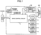
- FIG. 1 is a block diagram illustrating an example of a configuration of a semiconductor device according to a first embodiment
- FIG. 2 is a plan view illustrating a schematic configuration of the semiconductor device
- FIG. 3 is a plan view illustrating a detailed configuration of the semiconductor device
- FIG. 4 is a perspective view illustrating a schematic configuration of a resistive element
- FIG. 5 is a view illustrating a circuit configuration in a front surface layer (first layer) of the substrate
- FIG. 6 is a view illustrating a circuit configuration in a rear surface layer (eighth layer) of the substrate
- FIG. 7 is a view illustrating a configuration of wiring lines connecting a drive control circuit to NAND memories, and is a conceptual view of a layer structure of the substrate;
- FIG. 8 is a bottom view illustrating a schematic configuration of a semiconductor device according to a first modification of the first embodiment
- FIG. 9 is a view illustrating a configuration of wiring lines connecting a drive control circuit to NAND memories, and is a conceptual view of a layer structure of the substrate;
- FIG. 10 is a plan view illustrating a detailed configuration of a semiconductor device according to a second embodiment
- FIG. 11 is a cross-sectional view taken along line A-A of FIG. 10 in the direction of an arrow;
- FIG. 12 is a bottom view illustrating a schematic configuration of a semiconductor device according to a first modification of the second embodiment
- FIG. 13 is a cross-sectional view taken along line B-B of FIG. 12 in the direction of an arrow;
- FIG. 14 is a plan view illustrating a schematic configuration of a semiconductor device according to a third embodiment
- FIG. 15 is a view illustrating a bottom surface of a NAND memory
- FIG. 16 is a bottom view illustrating a schematic configuration of a semiconductor device according to a first modification of the third embodiment
- FIG. 17 is a plan view illustrating a schematic configuration of a semiconductor device according to a fourth embodiment.
- FIG. 18 is a bottom view illustrating a schematic configuration of a semiconductor device according to a first modification of the fourth embodiment.
- a semiconductor device includes a substrate, a connector, a volatile semiconductor memory element, nonvolatile semiconductor memory elements, and a controller.
- the substrate is a multi-layered structure with a wiring pattern formed therein, and has an almost rectangular shape in a plan view.
- the connector is provided on a short side of the surface to be connectable to a host device.
- the volatile semiconductor memory element is provided on the front surface layer side of the substrate.
- the nonvolatile semiconductor memory elements are provided on the front surface layer side of the substrate.
- the controller is provided on the front surface layer side of the substrate to control the volatile semiconductor memory element and the nonvolatile semiconductor memory element.
- the wiring pattern includes signal lines formed between the connector and the controller to connect the connector and the controller to each other. On the opposite side of the controller to the signal lines, multiple nonvolatile semiconductor memory elements are aligned along the longitudinal direction of the substrate.
- FIG. 1 is a block diagram illustrating an exemplary configuration of a semiconductor device according to a first embodiment.
- a semiconductor device 100 is connected to a host device (hereinafter, abbreviated as a host) 1 such as a personal computer or a CPU through a memory connection interface such as a SATA interface (ATA I/F) 2 , and functions as an external memory of the host 1 .
- a host device hereinafter, abbreviated as a host
- ATA I/F SATA interface
- the semiconductor device 100 can perform data communication with a debugging device 200 through a communication interface 3 such as RS232C interface (RS232C I/F).
- the semiconductor device 100 includes NAND-type flash memories (hereinafter, abbreviated as NAND memories) 10 serving as the nonvolatile semiconductor memory elements, a drive control circuit 4 serving as the controller, a DRAM 20 which is a volatile semiconductor memory element capable of a higher-speed memory operation than the NAND memories 10 , a power supply circuit 5 , an LED 6 for status display, and a temperature sensor 7 for detecting an internal temperature of a drive.
- the temperature sensor 7 directly or indirectly measures, for example, the temperature of the NAND memories 10 .
- the drive control circuit 4 restricts information writing and the like on the NAND memories 10 so as to suppress the temperature from rising any further.
- a non volatile semiconductor memory element such as MRAM (Magneto resistive Random Access Memory) for example, may be used instead of the DRAM 20 .
- the power supply circuit 5 generates multiple different internal DC power voltages from an external DC power supplied from a power supply circuit on the host 1 side, and supplies the internal DC power voltages to individual circuits in the semiconductor device 100 . Further, the power supply circuit 5 senses the rise of the external power, generates a power-on/reset signal, and provides the power-on/reset signal to the drive control circuit 4 .
- FIG. 2 is a plan view illustrating the schematic configuration of the semiconductor device 100 .
- FIG. 3 is a plan view illustrating the detailed configuration of the semiconductor device 100 .
- the power supply circuit 5 , the DRAM 20 , the drive control circuit 4 , and the NAND memories 10 are mounted on the substrate 8 with the wiring pattern formed therein.
- the substrate 8 has an almost rectangular shape in a plan view.
- a connector 9 is provided to be connected to the host 1 .
- the connector 9 functions as the above-mentioned SATA interface 2 and the communication interface 3 .
- the connector 9 also functions as a power input unit supplying the power input from the host 1 to the power supply circuit 5 .
- the connector 9 is, for example, a LIF connector.
- the connector 9 has a slit 9 a formed at a position deviating from the center of the substrate 8 in the widthwise direction of the substrate 8 such that, for example, a protrusion (not illustrated) provided on the host 1 side fits in the slit 9 a . Therefore, it is possible to prevent the semiconductor device 100 from being installed upside down.
- the substrate 8 is a multi-layered structure formed by stacking synthetic resins, for example, it is an 8-layer structure. However, the number of layers of the substrate 8 is not limited to 8.
- the wiring pattern is formed in various shapes on the surface or in the inside of each layer made of a synthetic resin. The wiring pattern formed in the substrate 8 electrically connects the power supply circuit 5 , the DRAM 20 , the drive control circuit 4 , and the NAND memories 10 mounted on the substrate 8 , to one another.
- the layout of the power supply circuit 5 , the DRAM 20 , the drive control circuit 4 , and the NAND memories 10 relative to the substrate 8 will be described.
- the power supply circuit 5 and the DRAM 20 are disposed near the connector 9 .
- the drive control circuit 4 is disposed next to the power supply circuit 5 and the DRAM 20 .
- the NAND memories 10 are disposed next to the drive control circuit 4 . That is, along the longitudinal direction of the substrate 8 from the connector 9 side, the DRAM 20 , the drive control circuit 4 , and the NAND memories 10 are disposed in this order.
- the multiple NAND memories 10 are mounted on the substrate 8 , and the multiple NAND memories 10 are disposed side by side along the longitudinal direction of the substrate 8 . In the first embodiment, four NAND memories 10 are disposed. However, as long as the number of NAND memories 10 is plural, the number of mounted NAND memories 10 is not limited thereto.
- two NAND memories 10 may be disposed on one long side of the substrate 8 , and the other two NAND memories 10 may be disposed on the other long side of the substrate 8 .
- FIG. 4 is a perspective view illustrating the schematic configuration of the resistive element 12 .
- the resistive element 12 is formed in such a form in which multiple resistive films 12 provided between electrodes 12 c are collectively covered with a protective coat 12 b .
- Each NAND memory 10 is provided with one resistive element 12 . Further, each resistive element 12 is disposed near the corresponding NAND memory 10 connected to the resistive element 12 .
- the wiring pattern formed in the substrate 8 will be described. As illustrated in FIG. 3 , between the power supply circuit 5 and the drive control circuit 4 , there is a region S where nearly no electronic components and the like are mounted. In the region S of the substrate 8 , signal lines (SATA signal lines) to connect the connector 9 to the drive control circuit 4 is formed as a portion of the wiring pattern. As described above, on the substrate 8 , on the connector 9 side relative to the drive control circuit 4 , the SATA signal lines 14 are formed, and on the opposite side of the drive control circuit 4 to the connector 9 , the NAND memories 10 are disposed side by side in a line along the longitudinal direction of the substrate 8 .
- SATA signal lines SATA signal lines
- FIG. 5 is a view illustrating the circuitry configuration on a front surface layer (first layer) L 1 of the substrate 8 .
- FIG. 6 is a view illustrating the circuitry configuration on a rear surface layer (eighth layer) L 8 of the substrate 8 .
- the SATA signal lines 14 are formed along the way from the position where the drive control circuit 4 is disposed near the connector 9 . Further, the SATA signal lines further extend from there through the via-holes 15 , which are formed to pass through the substrate 8 in the vicinity of the connector 9 . Then the SATA signal lines are connected to SATA signal lines 14 formed on the rear surface layer L 8 of the substrate 8 , thereby finally reaching the connector 9 .
- it is necessary to provide an electrode for the connector on the rear surface layer side of the substrate 8 it is required to form the SATA signal lines 14 to extend through the substrate 8 up to the rear surface layer L 8 as described above.
- the most region of the rear surface layer L 8 of the substrate 8 is a ground 18 . Further, although not illustrated, in inside layers between the front surface layer L 1 and the rear surface layer L 8 of the substrate 8 , in portions overlapping the SATA signal lines 14 , nearly no wiring patterns other than SATA signal lines 14 are formed. That is, in the portion overlapping the region S in the substrate 8 , no wiring patterns other than the SATA signal lines 14 are formed.
- the SATA signal lines 14 are partially broken on the front surface layer L 1 , but this is not especially problematic because signals running through the SATA signal lines 14 are relayed by relay terminals 16 (see FIG. 3 ) mounted on the corresponding portions on the substrate 8 . Furthermore, the front surface of the substrate 8 is covered with a protective coat (not illustrated) with an insulating property, such that the wiring pattern formed on the front surface layer L 1 is surely insulated.
- FIG. 7 is a view illustrating the configuration of wiring lines connecting the drive control circuit 4 to the NAND memories 10 , and is the conceptual view of a layer structure of the substrate 8 .
- FIG. 7 in order to simplify the drawing, a portion of the layer structure of the substrate 8 is not illustrated.
- the wiring line to connect the drive control circuit 4 to the resistive element 12 is connected to the drive control circuit 4 on the front surface layer of the substrate 8 and extends up to the inside layers of the substrate 8 through via-holes 21 .
- the wiring line runs around the inside layers, then extends further to the front surface layer through via-holes 22 again, and is connected to the resistive element 12 .
- the wiring line to connect the resistive element 12 to the NAND memory 10 is connected to the resistive element 12 on the front surface layer of the substrate 8 , and then extends up to the inside layers of the substrate 8 through via-holes 23 .
- the wiring line runs around the inside layers of the substrate 8 , then extends further up to the front surface layer of the substrate 8 through via-holes 24 , and is connected to the NAND memory 10 .
- the wiring line connecting the resistive element 12 to the NAND memory 10 is shorter than the wiring line connecting the drive control circuit 4 to the resistive element 12 .
- the semiconductor device 100 since the semiconductor device 100 includes the multiple NAND memories, multiple wiring lines are formed in the substrate 8 to connect the resistive elements 12 to the NAND memories 10 . Since the resistive elements 12 are disposed near the corresponding NAND memories 10 , a variation in length of multiple wiring lines connecting the resistive elements 12 to the NAND memories 10 is suppressed.
- the power supply circuit 5 , the drive control circuit 4 , the DRAM 20 , the NAND memories 10 , and the SATA signal lines 14 are disposed as described above, whereby it is possible to appropriately dispose those elements on the substrate 8 having an almost rectangular shape in a plan view.
- the power supply circuit 5 is disposed near the connector 9 , bypassing the SATA signal lines 14 . This makes it difficult for noise generated from the power supply circuit 5 to influence other elements or the SATA signal lines 14 , and improves the stability of the operation of the semiconductor device 100 .
- the DRAM 20 is disposed to bypass the SATA signal lines 14 . This makes it difficult for noise generated from the DRAM 20 to influence other elements or the SATA signal lines 14 , and improves the stability of the operation of the semiconductor device 100 .
- the DRAM 20 In general, it is preferable to dispose the DRAM 20 near the drive control circuit 4 . In the first embodiment, since the DRAM 20 is disposed near the drive control circuit 4 , it is possible to suppress deterioration of the performance characteristic of the semiconductor device 100 .
- NAND memories 10 are disposed on one long side of the substrate 8 , and the other two NAND memories 10 are disposed on the other long side of the substrate 8 .
- This configuration makes it possible to suppress the wiring pattern from being one-sided in the substrate 8 and to form the wiring pattern in balance.
- the resistive elements 12 are disposed near the corresponding NAND memories 10 , a variation in length of the multiple wiring lines connecting the resistive elements 12 to the NAND memories 10 is suppressed and thus it is possible to suppress deterioration of the performance characteristic of the semiconductor device 100 .
- the most region of the rear surface layer L 8 of the substrate 8 is a ground 18 , in a case where a device of the host 1 exists on the rear surface layer side of the semiconductor device 100 in a state in which the semiconductor device 100 is inserted into the host 1 , it is possible to suppress noise from the device from influencing each element, such as the wiring pattern and the NAND memories 10 , of the semiconductor device 100 . Similarly, it is difficult that noise from the wiring line and each element of the semiconductor device 100 influences the device on the host 1 side.
- the wiring pattern except for the SATA signal lines 14 is rarely formed. Therefore, it is possible to easily manage impedance relative to the SATA signal lines 14 .
- the substrate 8 having the eight-layer structure is given as an example.
- the present invention is not limited thereto.
- the number of layers of the substrate 8 may be changed.
- FIG. 8 is a bottom view illustrating the schematic configuration of a semiconductor device 100 according to a first modification of the first embodiment.
- FIG. 9 is a view illustrating the configuration of wiring lines connecting a drive control circuit 4 to NAND memories 10 , and is a conceptual view of a layer structure of the substrate 8 . In FIG. 9 , in order to simplify the drawing, a portion of the layer structure of the substrate 8 is not illustrated.
- NAND memories 10 are mounted, such that the semiconductor device 100 includes eight NAND memories 10 .
- the NAND memories 10 mounted on the rear surface layer side of the substrate 8 are disposed to be symmetrical to the NAND memories 10 mounted on the front surface layer side of the substrate 8 .
- the resistive elements 12 are not mounted on the rear surface layer side of the substrate 8 but only on the front surface layer. Therefore, wiring lines to connect the resistive elements 12 to the NAND memories 10 are formed to run around the inside layers of the substrate 8 , are divided by the via-holes 24 , and are present not only on the front surface layer L 1 of the substrate 8 but also on the rear surface layer L 8 .
- the wiring lines on the front surface layer L 1 are connected to the NAND memories 10 mounted on the front surface layer side, and the wiring lines on the rear surface layer L 8 are connected to the NAND memories 10 mounted on the rear surface layer side. That is, two NAND memories 10 are connected to one resistive element 12 .
- the NAND memories 10 are mounted on the both surfaces of the substrate 8 , increasing the memory capacity of the semiconductor device 100 . Further, it is possible to connect multiple (two in the modification) NAND memories 10 to each resistive element 12 by dividing the wiring line in the middle of it, and thus the semiconductor device 100 can include NAND memories 10 which are more than, in number, channels which the drive control circuit 4 has. In this modification, the drive control circuit 4 has four channels. In this case, eight NAND memories 10 can be incorporated. Further, each of two NAND memories 10 connected to one wiring line determines which of them operates, on the basis of whether a channel enable (CE) signal of the corresponding NAND memory is active or not.
- CE channel enable
- FIG. 10 is a plan view illustrating a detailed configuration of a semiconductor device according to a second embodiment.
- FIG. 11 is a cross-sectional view taken along line A-A of FIG. 10 in the direction of an arrow.
- the same components as in the above-mentioned embodiment are denoted by same reference symbols and the detailed description thereof is not repeated.
- a semiconductor device 102 has four NAND memories 10 all of which are disposed side by side on one long side of a substrate 8 , more specifically, on a long side where a power supply circuit 5 is provided. Since all of the NAND memories 10 are collectively disposed on one long side, in an empty space on the other long side, resistive elements 12 may be collectively disposed.
- the NAND memories 10 are configured to be higher than the other elements mounted on the substrate 8 . For this reason, of a region T along the other long side of the substrate 8 , in a portion where the resistive elements 12 are collectively disposed, as illustrated in FIG. 11 , it is possible to suppress the height of the semiconductor device 102 to be lower than a region U where the NAND memories 10 are disposed.
- the NAND memories 10 may be disposed to bypass the corresponding region, thereby obtaining the semiconductor device 102 satisfying the demand.
- the region along the other long side of the substrate 8 should be lower than the other region is given an example.
- a DRAM 20 and a temperature sensor 7 are also disposed in the region T.
- the DRAM 20 and the temperature sensor 7 are configured to be lower than the NAND memories 10 , it is possible to suppress the height of the semiconductor device 102 in the entire region T to be lower than the region U.
- FIG. 12 is a bottom view illustrating a schematic configuration of a semiconductor device 102 according to a first modification of the second embodiment.
- NAND memories 10 are disposed on the rear surface layer side of the substrate 8 to be symmetric to the NAND memories 10 disposed on the front surface layer side. Therefore, it is possible to increase the memory capability of the semiconductor device 102 .
- the NAND memories 10 are disposed to be symmetric to the NAND memories 10 disposed on the front surface layer side of the substrate 8 , even on the rear surface layer side of the substrate 8 , the NAND memories 10 are disposed on one long side. Therefore, it is possible to suppress the height of the semiconductor device 102 in the region T to be low.
- FIG. 14 is a plan view illustrating a schematic configuration of a semiconductor device according to a third embodiment.
- the same components as the above-mentioned embodiments are denoted by identical reference symbols and a detailed description thereof is omitted.
- two NAND memories 10 are disposed, and on the opposite side, two NAND memories 10 are further disposed. That is, along the longitudinal direction of the substrate 8 , multiple NAND memories 10 are disposed with the drive control circuit 4 interposed therebetween.
- the NAND memories 10 are separately disposed as described above, and thus it is possible to suppress a deviation in length among wiring lines connecting the NAND memories 10 and the drive control circuit 4 , as compared to a case where four NAND memories 10 are disposed side by side on one side of the drive control circuit 4 .
- the ratio of the shortest wiring line to the longest wiring line is about 1:4.
- the deviation in length among the wiring lines is suppressed, and thus it is possible to reduce a difference in optimal driver setting for the NAND memories 10 . Therefore, it is possible to suppress error generation of data and to stabilize the operation of the semiconductor device 103 .
- the NAND memories 10 provided on the connector 9 side relative to the drive control circuit 4 are mounted on SATA signal lines 14 .
- BGA ball grid array
- the NAND memories 10 in a case of forming the SATA signal lines 14 on the front surface layer L 1 , it is necessary to bypass ball-shaped electrodes (bumps) formed on the NAND memories 10 .
- the SATA signal lines 14 to connect the connector 9 and the drive control circuit 4 are formed in the inside layers of the substrate 8 .
- the NAND memories 10 are disposed on one long side of the substrate 8 , it is possible to suppress the height of the semiconductor device 103 in a region along the other long side. Further, the resistive elements 12 are disposed in the vicinities of the NAND memories 10 and thus it is possible to suppress deterioration of the performance characteristic of the semiconductor device 103 . Furthermore, the number of the NAND memories 10 which the semiconductor device 103 has is not limited to four, but may be two or more.
- FIG. 16 is a bottom view illustrating a schematic configuration of a semiconductor device according to a first modification of the third embodiment.
- NAND memories 10 are disposed on the rear surface layer side of the substrate 8 to be symmetric to the NAND memories 10 disposed on the front surface layer side. Therefore, it is possible to increase the memory capability of the semiconductor device 103 .
- the NAND memories 10 are disposed to be symmetric to the NAND memories 10 disposed on the front surface layer side of the substrate 8 , even on the rear surface layer side of the substrate 8 , the NAND memories 10 are disposed on one long side. Therefore, it is possible to suppress the height of the semiconductor device 102 in a region along the other long side to be low.
- FIG. 17 is a plan view illustrating a schematic configuration of a semiconductor device according to a fourth embodiment.
- the same components as the above-mentioned embodiments are denoted by identical reference symbols and a detailed description thereof is omitted.
- one NAND memory 10 is disposed, and on the opposite side, one NAND memory 10 is further disposed. That is, a semiconductor device 104 has two NAND memories 10 .
- the ratio of the shortest wiring line to the longest wiring line is about 1:2.
- the lengths of the multiple wiring lines are made substantially the same, and thus it is also possible to make optical driver setting for the NAND memories 10 substantially the same. Therefore, it is possible to suppress error generation of data and to stabilize the operation of the semiconductor device 104 .
- the SATA signal lines 14 are formed in the inside layers of the substrate 8 .
- the NAND memories 10 are disposed on one long side of the substrate 8 , it is possible to suppress the height of the semiconductor device 104 in a region along the other long side to be low.
- the resistive elements 12 are disposed in the vicinities of the NAND memories 10 and thus it is possible to suppress deterioration of the performance characteristic of the semiconductor device 104 .
- FIG. 18 is a bottom view illustrating a schematic configuration of the semiconductor device according to a first modification of the fourth embodiment.
- NAND memories 10 are disposed on the rear surface layer side of the substrate 8 to be symmetric to the NAND memories 10 disposed on the front surface layer side. Therefore, it is possible to increase the memory capability of the semiconductor device 104 .
- the NAND memories 10 are disposed to be symmetric to the NAND memories 10 disposed on the front surface layer side of the substrate 8 , even on the rear surface layer side of the substrate 8 , the NAND memories 10 are disposed on one long side. Therefore, it is possible to suppress the height of the semiconductor device 104 in a region along the other long side to be low.
Abstract
Description
Claims (18)
Priority Applications (1)
| Application Number | Priority Date | Filing Date | Title |
|---|---|---|---|
| US13/731,613 US8665624B2 (en) | 2011-02-23 | 2012-12-31 | Semiconductor device |
Applications Claiming Priority (4)
| Application Number | Priority Date | Filing Date | Title |
|---|---|---|---|
| JP2011037344A JP5396415B2 (en) | 2011-02-23 | 2011-02-23 | Semiconductor device |
| JP2011-037344 | 2011-02-23 | ||
| US13/052,425 US8379427B2 (en) | 2011-02-23 | 2011-03-21 | Semiconductor device |
| US13/731,613 US8665624B2 (en) | 2011-02-23 | 2012-12-31 | Semiconductor device |
Related Parent Applications (1)
| Application Number | Title | Priority Date | Filing Date |
|---|---|---|---|
| US13/052,425 Continuation US8379427B2 (en) | 2011-02-23 | 2011-03-21 | Semiconductor device |
Publications (2)
| Publication Number | Publication Date |
|---|---|
| US20130121074A1 US20130121074A1 (en) | 2013-05-16 |
| US8665624B2 true US8665624B2 (en) | 2014-03-04 |
Family
ID=46652605
Family Applications (13)
| Application Number | Title | Priority Date | Filing Date |
|---|---|---|---|
| US13/052,425 Active 2031-07-28 US8379427B2 (en) | 2011-02-23 | 2011-03-21 | Semiconductor device |
| US13/731,613 Active US8665624B2 (en) | 2011-02-23 | 2012-12-31 | Semiconductor device |
| US13/731,599 Active US8611126B2 (en) | 2011-02-23 | 2012-12-31 | Semiconductor device |
| US13/954,254 Active US8817513B2 (en) | 2011-02-23 | 2013-07-30 | Semiconductor device |
| US14/328,552 Active 2031-06-06 US9449654B2 (en) | 2011-02-23 | 2014-07-10 | Semiconductor device |
| US14/731,712 Active US9373363B2 (en) | 2011-02-23 | 2015-06-05 | Semiconductor device |
| US15/646,360 Active US10056119B2 (en) | 2011-02-23 | 2017-07-11 | Semiconductor device |
| US16/044,912 Active US10339981B2 (en) | 2011-02-23 | 2018-07-25 | Semiconductor device |
| US16/423,665 Active US10566033B2 (en) | 2011-02-23 | 2019-05-28 | Semiconductor device |
| US16/736,945 Active US10847190B2 (en) | 2011-02-23 | 2020-01-08 | Semiconductor device |
| US17/077,560 Active US11244708B2 (en) | 2011-02-23 | 2020-10-22 | Semiconductor device |
| US17/565,713 Active US11735230B2 (en) | 2011-02-23 | 2021-12-30 | Semiconductor device |
| US18/347,517 Pending US20230343371A1 (en) | 2011-02-23 | 2023-07-05 | Semiconductor device |
Family Applications Before (1)
| Application Number | Title | Priority Date | Filing Date |
|---|---|---|---|
| US13/052,425 Active 2031-07-28 US8379427B2 (en) | 2011-02-23 | 2011-03-21 | Semiconductor device |
Family Applications After (11)
| Application Number | Title | Priority Date | Filing Date |
|---|---|---|---|
| US13/731,599 Active US8611126B2 (en) | 2011-02-23 | 2012-12-31 | Semiconductor device |
| US13/954,254 Active US8817513B2 (en) | 2011-02-23 | 2013-07-30 | Semiconductor device |
| US14/328,552 Active 2031-06-06 US9449654B2 (en) | 2011-02-23 | 2014-07-10 | Semiconductor device |
| US14/731,712 Active US9373363B2 (en) | 2011-02-23 | 2015-06-05 | Semiconductor device |
| US15/646,360 Active US10056119B2 (en) | 2011-02-23 | 2017-07-11 | Semiconductor device |
| US16/044,912 Active US10339981B2 (en) | 2011-02-23 | 2018-07-25 | Semiconductor device |
| US16/423,665 Active US10566033B2 (en) | 2011-02-23 | 2019-05-28 | Semiconductor device |
| US16/736,945 Active US10847190B2 (en) | 2011-02-23 | 2020-01-08 | Semiconductor device |
| US17/077,560 Active US11244708B2 (en) | 2011-02-23 | 2020-10-22 | Semiconductor device |
| US17/565,713 Active US11735230B2 (en) | 2011-02-23 | 2021-12-30 | Semiconductor device |
| US18/347,517 Pending US20230343371A1 (en) | 2011-02-23 | 2023-07-05 | Semiconductor device |
Country Status (2)
| Country | Link |
|---|---|
| US (13) | US8379427B2 (en) |
| JP (1) | JP5396415B2 (en) |
Families Citing this family (15)
| Publication number | Priority date | Publication date | Assignee | Title |
|---|---|---|---|---|
| JP5396415B2 (en) | 2011-02-23 | 2014-01-22 | 株式会社東芝 | Semiconductor device |
| US9659600B2 (en) | 2014-07-10 | 2017-05-23 | Sap Se | Filter customization for search facilitation |
| TW201250702A (en) * | 2011-06-14 | 2012-12-16 | Hon Hai Prec Ind Co Ltd | Solid state drive |
| CN102855912A (en) * | 2011-06-30 | 2013-01-02 | 鸿富锦精密工业(深圳)有限公司 | Solid state drive |
| CN102890964B (en) * | 2011-07-21 | 2015-10-07 | 光宝科技股份有限公司 | Solid state storage device and corresponding control methods thereof |
| CN103000214A (en) * | 2011-09-15 | 2013-03-27 | 鸿富锦精密工业(深圳)有限公司 | Solid state drive combination |
| US9460813B2 (en) | 2013-03-14 | 2016-10-04 | Kabushiki Kaisha Toshiba | Memory system |
| CN104346232A (en) * | 2013-08-06 | 2015-02-11 | 慧荣科技股份有限公司 | Data storage device and access limiting method thereof |
| JP2015122924A (en) * | 2013-12-25 | 2015-07-02 | 株式会社東芝 | Semiconductor system, power supply component, and semiconductor component |
| US10001963B2 (en) * | 2015-12-01 | 2018-06-19 | Alson Technology Limited | Dynamic random access memory |
| US10714148B2 (en) * | 2015-12-30 | 2020-07-14 | Shenzhen Longsys Electronics Co., Ltd. | SSD storage module, SSD component, and SSD |
| WO2018013900A1 (en) | 2016-07-15 | 2018-01-18 | Momentive Performance Materials Inc. | Method of stabilizing imino-functional silane |
| TWI645623B (en) * | 2017-09-30 | 2018-12-21 | 慧榮科技股份有限公司 | Memory device |
| JP7385113B2 (en) | 2019-10-21 | 2023-11-22 | 株式会社バッファロー | semiconductor memory device |
| US11301401B1 (en) * | 2020-12-18 | 2022-04-12 | Micron Technology, Inc. | Ball grid array storage for a memory sub-system |
Citations (12)
| Publication number | Priority date | Publication date | Assignee | Title |
|---|---|---|---|---|
| US6011741A (en) | 1991-04-11 | 2000-01-04 | Sandisk Corporation | Computer memory cards using flash EEPROM integrated circuit chips and memory-controller systems |
| JP2005150490A (en) | 2003-11-18 | 2005-06-09 | Canon Inc | Sheet component between ic and printed wiring board |
| JP3131669U (en) | 2007-02-28 | 2007-05-17 | オリオン電機株式会社 | Circuit board and display device |
| JP2008103462A (en) | 2006-10-18 | 2008-05-01 | Flat Denshi:Kk | Chip type network resistor, surface mounting component, and method for manufacturing the same |
| US7477522B2 (en) | 2006-10-23 | 2009-01-13 | International Business Machines Corporation | High density high reliability memory module with a fault tolerant address and command bus |
| JP2009010913A (en) | 2007-05-29 | 2009-01-15 | Shinko Electric Ind Co Ltd | Delay circuit, and delay time adjustment method |
| US7516903B2 (en) * | 2000-04-28 | 2009-04-14 | Renesas Technology Corp. | IC card |
| JP2009163409A (en) | 2007-12-28 | 2009-07-23 | Toshiba Corp | Semiconductor memory |
| US7581058B2 (en) | 2002-04-05 | 2009-08-25 | Renesas Technology Corp. | Non-volatile memory having multiple erase operations |
| JP2010061438A (en) | 2008-09-04 | 2010-03-18 | Sony Corp | Information processor |
| US20100073860A1 (en) | 2008-09-24 | 2010-03-25 | Takakatsu Moriai | Ssd apparatus |
| US8379427B2 (en) | 2011-02-23 | 2013-02-19 | Kabushiki Kaisha Toshiba | Semiconductor device |
Family Cites Families (38)
| Publication number | Priority date | Publication date | Assignee | Title |
|---|---|---|---|---|
| JPS5593029U (en) * | 1978-12-20 | 1980-06-27 | ||
| JP3438375B2 (en) | 1994-02-15 | 2003-08-18 | 株式会社日立製作所 | Signal transmission device and signal receiving module |
| JPH07282217A (en) * | 1994-04-13 | 1995-10-27 | Canon Inc | Storage device |
| JPH07325898A (en) | 1994-06-02 | 1995-12-12 | Hitachi Ltd | Storage device |
| JPH09147545A (en) | 1995-09-19 | 1997-06-06 | Ricoh Co Ltd | Memory card and information processing device |
| US5661677A (en) | 1996-05-15 | 1997-08-26 | Micron Electronics, Inc. | Circuit and method for on-board programming of PRD Serial EEPROMS |
| JP3957237B2 (en) | 1998-01-19 | 2007-08-15 | 富士通株式会社 | Integrated circuit device module |
| JPH11251490A (en) * | 1998-03-03 | 1999-09-17 | Toshiba Corp | Semiconductor device and semiconductor package |
| JPH11251516A (en) | 1998-03-04 | 1999-09-17 | Hitachi Ltd | Semiconductor module |
| JP3914651B2 (en) | 1999-02-26 | 2007-05-16 | エルピーダメモリ株式会社 | Memory module and manufacturing method thereof |
| JP4487352B2 (en) | 1999-11-12 | 2010-06-23 | ソニー株式会社 | Communication terminal device |
| JP3815936B2 (en) * | 2000-01-25 | 2006-08-30 | 株式会社ルネサステクノロジ | IC card |
| JP2002026073A (en) | 2000-07-07 | 2002-01-25 | Hitachi Ltd | Semiconductor device and its manufacturing method |
| CN100426417C (en) * | 2001-07-17 | 2008-10-15 | 三洋电机株式会社 | Semiconductor memory device |
| JP4094370B2 (en) | 2002-07-31 | 2008-06-04 | エルピーダメモリ株式会社 | Memory module and memory system |
| US6646948B1 (en) * | 2002-08-29 | 2003-11-11 | Motorola, Inc. | Data storage system utilizing a non-volatile IC based memory for reduction of data retrieval time |
| JP4234529B2 (en) * | 2003-08-12 | 2009-03-04 | 株式会社東芝 | Cable modem module device and electronic device |
| JP2006049411A (en) | 2004-08-02 | 2006-02-16 | Toshiba Mach Co Ltd | Method and device for monitoring joining section of power element by estimating temperature rise of the section |
| JP4632122B2 (en) | 2004-12-16 | 2011-02-16 | エルピーダメモリ株式会社 | module |
| JP4811905B2 (en) | 2005-02-25 | 2011-11-09 | ローム株式会社 | Semiconductor light emitting device |
| JP4674850B2 (en) | 2005-02-25 | 2011-04-20 | ルネサスエレクトロニクス株式会社 | Semiconductor device |
| JP2007102977A (en) * | 2005-10-07 | 2007-04-19 | Toshiba Corp | Semiconductor memory apparatus |
| JP4389228B2 (en) | 2006-11-29 | 2009-12-24 | エルピーダメモリ株式会社 | Memory module |
| JP5409996B2 (en) * | 2006-12-25 | 2014-02-05 | ピーエスフォー ルクスコ エスエイアールエル | Multilayer printed wiring board |
| KR101257912B1 (en) | 2007-02-14 | 2013-04-24 | 삼성전자주식회사 | Semiconductor memory device and method of arranging terminals of the same, and memory module comprising the device and method of arranging terminals and lines on board of the same |
| JP4447615B2 (en) | 2007-02-19 | 2010-04-07 | 株式会社ルネサステクノロジ | Semiconductor module |
| US7644216B2 (en) * | 2007-04-16 | 2010-01-05 | International Business Machines Corporation | System and method for providing an adapter for re-use of legacy DIMMS in a fully buffered memory environment |
| JP4544281B2 (en) | 2007-08-31 | 2010-09-15 | ソニー株式会社 | Card type peripheral device |
| JP5579369B2 (en) | 2008-01-24 | 2014-08-27 | ピーエスフォー ルクスコ エスエイアールエル | Semiconductor device |
| JP2010080744A (en) * | 2008-09-26 | 2010-04-08 | Fujitsu Ltd | Printed circuit board and electronic apparatus |
| JP4575484B2 (en) | 2008-09-26 | 2010-11-04 | 株式会社東芝 | Storage device and storage device control method |
| KR20100041515A (en) * | 2008-10-14 | 2010-04-22 | 삼성전자주식회사 | Method for testing a solid state drive having a removable auxiliary test terminals |
| US7826181B2 (en) * | 2008-11-12 | 2010-11-02 | Seagate Technology Llc | Magnetic memory with porous non-conductive current confinement layer |
| US8472199B2 (en) | 2008-11-13 | 2013-06-25 | Mosaid Technologies Incorporated | System including a plurality of encapsulated semiconductor chips |
| JP5473317B2 (en) | 2008-12-24 | 2014-04-16 | ピーエスフォー ルクスコ エスエイアールエル | Memory module and layout method thereof |
| JP4679656B2 (en) | 2009-08-31 | 2011-04-27 | 株式会社東芝 | Information processing apparatus and nonvolatile semiconductor memory drive |
| TWM375289U (en) * | 2009-10-01 | 2010-03-01 | Orient Semiconductor Elect Ltd | Package for electronic storage device |
| KR101921619B1 (en) | 2009-12-28 | 2018-11-26 | 가부시키가이샤 한도오따이 에네루기 켄큐쇼 | Method for manufacturing semiconductor device |
-
2011
- 2011-02-23 JP JP2011037344A patent/JP5396415B2/en active Active
- 2011-03-21 US US13/052,425 patent/US8379427B2/en active Active
-
2012
- 2012-12-31 US US13/731,613 patent/US8665624B2/en active Active
- 2012-12-31 US US13/731,599 patent/US8611126B2/en active Active
-
2013
- 2013-07-30 US US13/954,254 patent/US8817513B2/en active Active
-
2014
- 2014-07-10 US US14/328,552 patent/US9449654B2/en active Active
-
2015
- 2015-06-05 US US14/731,712 patent/US9373363B2/en active Active
-
2017
- 2017-07-11 US US15/646,360 patent/US10056119B2/en active Active
-
2018
- 2018-07-25 US US16/044,912 patent/US10339981B2/en active Active
-
2019
- 2019-05-28 US US16/423,665 patent/US10566033B2/en active Active
-
2020
- 2020-01-08 US US16/736,945 patent/US10847190B2/en active Active
- 2020-10-22 US US17/077,560 patent/US11244708B2/en active Active
-
2021
- 2021-12-30 US US17/565,713 patent/US11735230B2/en active Active
-
2023
- 2023-07-05 US US18/347,517 patent/US20230343371A1/en active Pending
Patent Citations (14)
| Publication number | Priority date | Publication date | Assignee | Title |
|---|---|---|---|---|
| US6011741A (en) | 1991-04-11 | 2000-01-04 | Sandisk Corporation | Computer memory cards using flash EEPROM integrated circuit chips and memory-controller systems |
| US7516903B2 (en) * | 2000-04-28 | 2009-04-14 | Renesas Technology Corp. | IC card |
| US7581058B2 (en) | 2002-04-05 | 2009-08-25 | Renesas Technology Corp. | Non-volatile memory having multiple erase operations |
| JP2005150490A (en) | 2003-11-18 | 2005-06-09 | Canon Inc | Sheet component between ic and printed wiring board |
| JP2008103462A (en) | 2006-10-18 | 2008-05-01 | Flat Denshi:Kk | Chip type network resistor, surface mounting component, and method for manufacturing the same |
| US7477522B2 (en) | 2006-10-23 | 2009-01-13 | International Business Machines Corporation | High density high reliability memory module with a fault tolerant address and command bus |
| JP3131669U (en) | 2007-02-28 | 2007-05-17 | オリオン電機株式会社 | Circuit board and display device |
| JP2009010913A (en) | 2007-05-29 | 2009-01-15 | Shinko Electric Ind Co Ltd | Delay circuit, and delay time adjustment method |
| JP2009163409A (en) | 2007-12-28 | 2009-07-23 | Toshiba Corp | Semiconductor memory |
| US20100153625A1 (en) | 2007-12-28 | 2010-06-17 | Kabushiki Kaisha Toshiba | Semiconductor memory device |
| JP2010061438A (en) | 2008-09-04 | 2010-03-18 | Sony Corp | Information processor |
| US20100073860A1 (en) | 2008-09-24 | 2010-03-25 | Takakatsu Moriai | Ssd apparatus |
| JP2010079445A (en) | 2008-09-24 | 2010-04-08 | Toshiba Corp | Ssd device |
| US8379427B2 (en) | 2011-02-23 | 2013-02-19 | Kabushiki Kaisha Toshiba | Semiconductor device |
Non-Patent Citations (6)
| Title |
|---|
| "Disassemble New MacBook Air-investigate a secret of thinness and competitive price", Nikkei Electronics, Nikkei Business Publications, Inc., No. 1045, Dec. 13, 2010, pp. 83-90. |
| "Solid State Drives", Transcend, , 2 pages (with English Translation). |
| "Disassemble New MacBook Air—investigate a secret of thinness and competitive price", Nikkei Electronics, Nikkei Business Publications, Inc., No. 1045, Dec. 13, 2010, pp. 83-90. |
| "Solid State Drives", Transcend, <URL:http://www.transcend.co.jp/Products/CatList.asp?Func1No=1&FldNo=21>, 2 pages (with English Translation). |
| Office Action issued Jul. 2, 2013, in Japanese Patent Application No. 2011-037344 (with English-language translation). |
| Office Action mailed Apr. 3, 2013 in co-pending U.S. Appl. No. 13/731,599. |
Also Published As
| Publication number | Publication date |
|---|---|
| US20140321187A1 (en) | 2014-10-30 |
| US8817513B2 (en) | 2014-08-26 |
| US20220122640A1 (en) | 2022-04-21 |
| US10339981B2 (en) | 2019-07-02 |
| US20120212988A1 (en) | 2012-08-23 |
| US10056119B2 (en) | 2018-08-21 |
| US20130314991A1 (en) | 2013-11-28 |
| JP2012174126A (en) | 2012-09-10 |
| US9373363B2 (en) | 2016-06-21 |
| US20230343371A1 (en) | 2023-10-26 |
| JP5396415B2 (en) | 2014-01-22 |
| US8611126B2 (en) | 2013-12-17 |
| US20210043235A1 (en) | 2021-02-11 |
| US10847190B2 (en) | 2020-11-24 |
| US9449654B2 (en) | 2016-09-20 |
| US20150269973A1 (en) | 2015-09-24 |
| US8379427B2 (en) | 2013-02-19 |
| US11735230B2 (en) | 2023-08-22 |
| US20190279686A1 (en) | 2019-09-12 |
| US20130121073A1 (en) | 2013-05-16 |
| US10566033B2 (en) | 2020-02-18 |
| US20170309313A1 (en) | 2017-10-26 |
| US20200143848A1 (en) | 2020-05-07 |
| US20180330764A1 (en) | 2018-11-15 |
| US20130121074A1 (en) | 2013-05-16 |
| US11244708B2 (en) | 2022-02-08 |
Similar Documents
| Publication | Publication Date | Title |
|---|---|---|
| US11735230B2 (en) | Semiconductor device | |
| US9721621B2 (en) | Semiconductor device | |
| JP6672522B2 (en) | Semiconductor storage device | |
| JP7238177B2 (en) | system | |
| JP6833086B2 (en) | system | |
| JP6621503B2 (en) | Semiconductor memory device | |
| JP7023393B2 (en) | Semiconductor storage device | |
| JP7464769B2 (en) | Semiconductor memory device | |
| JP6381769B2 (en) | Semiconductor memory device | |
| JP6253824B2 (en) | Semiconductor memory device | |
| JP5940752B1 (en) | Semiconductor memory device | |
| JP5902335B2 (en) | Semiconductor memory device and system | |
| JP2023067900A (en) | semiconductor storage device | |
| JP2016181320A (en) | Semiconductor storage device | |
| JP2014059948A (en) | Semiconductor device |
Legal Events
| Date | Code | Title | Description |
|---|---|---|---|
| STCF | Information on status: patent grant |
Free format text: PATENTED CASE |
|
| FEPP | Fee payment procedure |
Free format text: PAYOR NUMBER ASSIGNED (ORIGINAL EVENT CODE: ASPN); ENTITY STATUS OF PATENT OWNER: LARGE ENTITY |
|
| AS | Assignment |
Owner name: TOSHIBA MEMORY CORPORATION, JAPAN Free format text: ASSIGNMENT OF ASSIGNORS INTEREST;ASSIGNOR:KABUSHIKI KAISHA TOSHIBA;REEL/FRAME:043088/0620 Effective date: 20170612 |
|
| MAFP | Maintenance fee payment |
Free format text: PAYMENT OF MAINTENANCE FEE, 4TH YEAR, LARGE ENTITY (ORIGINAL EVENT CODE: M1551) Year of fee payment: 4 |
|
| AS | Assignment |
Owner name: K.K. PANGEA, JAPAN Free format text: MERGER;ASSIGNOR:TOSHIBA MEMORY CORPORATION;REEL/FRAME:055659/0471 Effective date: 20180801 Owner name: TOSHIBA MEMORY CORPORATION, JAPAN Free format text: CHANGE OF NAME AND ADDRESS;ASSIGNOR:K.K. PANGEA;REEL/FRAME:055669/0401 Effective date: 20180801 Owner name: KIOXIA CORPORATION, JAPAN Free format text: CHANGE OF NAME AND ADDRESS;ASSIGNOR:TOSHIBA MEMORY CORPORATION;REEL/FRAME:055669/0001 Effective date: 20191001 |
|
| MAFP | Maintenance fee payment |
Free format text: PAYMENT OF MAINTENANCE FEE, 8TH YEAR, LARGE ENTITY (ORIGINAL EVENT CODE: M1552); ENTITY STATUS OF PATENT OWNER: LARGE ENTITY Year of fee payment: 8 |