US8669614B2 - Monolithic metal oxide semiconductor field effect transistor-Schottky diode device - Google Patents
Monolithic metal oxide semiconductor field effect transistor-Schottky diode device Download PDFInfo
- Publication number
- US8669614B2 US8669614B2 US13/349,572 US201213349572A US8669614B2 US 8669614 B2 US8669614 B2 US 8669614B2 US 201213349572 A US201213349572 A US 201213349572A US 8669614 B2 US8669614 B2 US 8669614B2
- Authority
- US
- United States
- Prior art keywords
- schottky diode
- mosfet
- region
- termination
- monolithic
- Prior art date
- Legal status (The legal status is an assumption and is not a legal conclusion. Google has not performed a legal analysis and makes no representation as to the accuracy of the status listed.)
- Expired - Fee Related, expires
Links
- 239000004065 semiconductor Substances 0.000 title claims abstract description 7
- 230000005669 field effect Effects 0.000 title claims abstract description 4
- 229910044991 metal oxide Inorganic materials 0.000 title claims abstract description 4
- 150000004706 metal oxides Chemical class 0.000 title claims abstract description 4
- 230000004888 barrier function Effects 0.000 claims description 8
- 230000009977 dual effect Effects 0.000 claims description 3
- 239000010410 layer Substances 0.000 description 51
- 239000000758 substrate Substances 0.000 description 19
- 239000000463 material Substances 0.000 description 12
- VYPSYNLAJGMNEJ-UHFFFAOYSA-N Silicium dioxide Chemical compound O=[Si]=O VYPSYNLAJGMNEJ-UHFFFAOYSA-N 0.000 description 5
- 238000009413 insulation Methods 0.000 description 5
- 229910052814 silicon oxide Inorganic materials 0.000 description 5
- 229910021420 polycrystalline silicon Inorganic materials 0.000 description 4
- RYGMFSIKBFXOCR-UHFFFAOYSA-N Copper Chemical compound [Cu] RYGMFSIKBFXOCR-UHFFFAOYSA-N 0.000 description 3
- 229910052782 aluminium Inorganic materials 0.000 description 3
- XAGFODPZIPBFFR-UHFFFAOYSA-N aluminium Chemical compound [Al] XAGFODPZIPBFFR-UHFFFAOYSA-N 0.000 description 3
- 229910052802 copper Inorganic materials 0.000 description 3
- 239000010949 copper Substances 0.000 description 3
- 239000011229 interlayer Substances 0.000 description 3
- 229910052751 metal Inorganic materials 0.000 description 3
- 239000002184 metal Substances 0.000 description 3
- 230000003071 parasitic effect Effects 0.000 description 3
- 230000008901 benefit Effects 0.000 description 2
- 230000003247 decreasing effect Effects 0.000 description 2
- 238000012986 modification Methods 0.000 description 2
- 230000004048 modification Effects 0.000 description 2
- 238000005516 engineering process Methods 0.000 description 1
- 230000000630 rising effect Effects 0.000 description 1
Images


Classifications
-
- H—ELECTRICITY
- H01—ELECTRIC ELEMENTS
- H01L—SEMICONDUCTOR DEVICES NOT COVERED BY CLASS H10
- H01L29/00—Semiconductor devices adapted for rectifying, amplifying, oscillating or switching, or capacitors or resistors with at least one potential-jump barrier or surface barrier, e.g. PN junction depletion layer or carrier concentration layer; Details of semiconductor bodies or of electrodes thereof ; Multistep manufacturing processes therefor
- H01L29/66—Types of semiconductor device ; Multistep manufacturing processes therefor
- H01L29/68—Types of semiconductor device ; Multistep manufacturing processes therefor controllable by only the electric current supplied, or only the electric potential applied, to an electrode which does not carry the current to be rectified, amplified or switched
- H01L29/76—Unipolar devices, e.g. field effect transistors
- H01L29/772—Field effect transistors
- H01L29/78—Field effect transistors with field effect produced by an insulated gate
- H01L29/7801—DMOS transistors, i.e. MISFETs with a channel accommodating body or base region adjoining a drain drift region
- H01L29/7802—Vertical DMOS transistors, i.e. VDMOS transistors
- H01L29/7811—Vertical DMOS transistors, i.e. VDMOS transistors with an edge termination structure
-
- H—ELECTRICITY
- H01—ELECTRIC ELEMENTS
- H01L—SEMICONDUCTOR DEVICES NOT COVERED BY CLASS H10
- H01L27/00—Devices consisting of a plurality of semiconductor or other solid-state components formed in or on a common substrate
- H01L27/02—Devices consisting of a plurality of semiconductor or other solid-state components formed in or on a common substrate including semiconductor components specially adapted for rectifying, oscillating, amplifying or switching and having at least one potential-jump barrier or surface barrier; including integrated passive circuit elements with at least one potential-jump barrier or surface barrier
- H01L27/04—Devices consisting of a plurality of semiconductor or other solid-state components formed in or on a common substrate including semiconductor components specially adapted for rectifying, oscillating, amplifying or switching and having at least one potential-jump barrier or surface barrier; including integrated passive circuit elements with at least one potential-jump barrier or surface barrier the substrate being a semiconductor body
- H01L27/06—Devices consisting of a plurality of semiconductor or other solid-state components formed in or on a common substrate including semiconductor components specially adapted for rectifying, oscillating, amplifying or switching and having at least one potential-jump barrier or surface barrier; including integrated passive circuit elements with at least one potential-jump barrier or surface barrier the substrate being a semiconductor body including a plurality of individual components in a non-repetitive configuration
- H01L27/0611—Devices consisting of a plurality of semiconductor or other solid-state components formed in or on a common substrate including semiconductor components specially adapted for rectifying, oscillating, amplifying or switching and having at least one potential-jump barrier or surface barrier; including integrated passive circuit elements with at least one potential-jump barrier or surface barrier the substrate being a semiconductor body including a plurality of individual components in a non-repetitive configuration integrated circuits having a two-dimensional layout of components without a common active region
- H01L27/0617—Devices consisting of a plurality of semiconductor or other solid-state components formed in or on a common substrate including semiconductor components specially adapted for rectifying, oscillating, amplifying or switching and having at least one potential-jump barrier or surface barrier; including integrated passive circuit elements with at least one potential-jump barrier or surface barrier the substrate being a semiconductor body including a plurality of individual components in a non-repetitive configuration integrated circuits having a two-dimensional layout of components without a common active region comprising components of the field-effect type
- H01L27/0629—Devices consisting of a plurality of semiconductor or other solid-state components formed in or on a common substrate including semiconductor components specially adapted for rectifying, oscillating, amplifying or switching and having at least one potential-jump barrier or surface barrier; including integrated passive circuit elements with at least one potential-jump barrier or surface barrier the substrate being a semiconductor body including a plurality of individual components in a non-repetitive configuration integrated circuits having a two-dimensional layout of components without a common active region comprising components of the field-effect type in combination with diodes, or resistors, or capacitors
-
- H—ELECTRICITY
- H01—ELECTRIC ELEMENTS
- H01L—SEMICONDUCTOR DEVICES NOT COVERED BY CLASS H10
- H01L29/00—Semiconductor devices adapted for rectifying, amplifying, oscillating or switching, or capacitors or resistors with at least one potential-jump barrier or surface barrier, e.g. PN junction depletion layer or carrier concentration layer; Details of semiconductor bodies or of electrodes thereof ; Multistep manufacturing processes therefor
- H01L29/02—Semiconductor bodies ; Multistep manufacturing processes therefor
- H01L29/06—Semiconductor bodies ; Multistep manufacturing processes therefor characterised by their shape; characterised by the shapes, relative sizes, or dispositions of the semiconductor regions ; characterised by the concentration or distribution of impurities within semiconductor regions
- H01L29/0603—Semiconductor bodies ; Multistep manufacturing processes therefor characterised by their shape; characterised by the shapes, relative sizes, or dispositions of the semiconductor regions ; characterised by the concentration or distribution of impurities within semiconductor regions characterised by particular constructional design considerations, e.g. for preventing surface leakage, for controlling electric field concentration or for internal isolations regions
- H01L29/0607—Semiconductor bodies ; Multistep manufacturing processes therefor characterised by their shape; characterised by the shapes, relative sizes, or dispositions of the semiconductor regions ; characterised by the concentration or distribution of impurities within semiconductor regions characterised by particular constructional design considerations, e.g. for preventing surface leakage, for controlling electric field concentration or for internal isolations regions for preventing surface leakage or controlling electric field concentration
- H01L29/0611—Semiconductor bodies ; Multistep manufacturing processes therefor characterised by their shape; characterised by the shapes, relative sizes, or dispositions of the semiconductor regions ; characterised by the concentration or distribution of impurities within semiconductor regions characterised by particular constructional design considerations, e.g. for preventing surface leakage, for controlling electric field concentration or for internal isolations regions for preventing surface leakage or controlling electric field concentration for increasing or controlling the breakdown voltage of reverse biased devices
- H01L29/0615—Semiconductor bodies ; Multistep manufacturing processes therefor characterised by their shape; characterised by the shapes, relative sizes, or dispositions of the semiconductor regions ; characterised by the concentration or distribution of impurities within semiconductor regions characterised by particular constructional design considerations, e.g. for preventing surface leakage, for controlling electric field concentration or for internal isolations regions for preventing surface leakage or controlling electric field concentration for increasing or controlling the breakdown voltage of reverse biased devices by the doping profile or the shape or the arrangement of the PN junction, or with supplementary regions, e.g. junction termination extension [JTE]
- H01L29/0619—Semiconductor bodies ; Multistep manufacturing processes therefor characterised by their shape; characterised by the shapes, relative sizes, or dispositions of the semiconductor regions ; characterised by the concentration or distribution of impurities within semiconductor regions characterised by particular constructional design considerations, e.g. for preventing surface leakage, for controlling electric field concentration or for internal isolations regions for preventing surface leakage or controlling electric field concentration for increasing or controlling the breakdown voltage of reverse biased devices by the doping profile or the shape or the arrangement of the PN junction, or with supplementary regions, e.g. junction termination extension [JTE] with a supplementary region doped oppositely to or in rectifying contact with the semiconductor containing or contacting region, e.g. guard rings with PN or Schottky junction
-
- H—ELECTRICITY
- H01—ELECTRIC ELEMENTS
- H01L—SEMICONDUCTOR DEVICES NOT COVERED BY CLASS H10
- H01L29/00—Semiconductor devices adapted for rectifying, amplifying, oscillating or switching, or capacitors or resistors with at least one potential-jump barrier or surface barrier, e.g. PN junction depletion layer or carrier concentration layer; Details of semiconductor bodies or of electrodes thereof ; Multistep manufacturing processes therefor
- H01L29/40—Electrodes ; Multistep manufacturing processes therefor
- H01L29/402—Field plates
- H01L29/404—Multiple field plate structures
-
- H—ELECTRICITY
- H01—ELECTRIC ELEMENTS
- H01L—SEMICONDUCTOR DEVICES NOT COVERED BY CLASS H10
- H01L29/00—Semiconductor devices adapted for rectifying, amplifying, oscillating or switching, or capacitors or resistors with at least one potential-jump barrier or surface barrier, e.g. PN junction depletion layer or carrier concentration layer; Details of semiconductor bodies or of electrodes thereof ; Multistep manufacturing processes therefor
- H01L29/66—Types of semiconductor device ; Multistep manufacturing processes therefor
- H01L29/68—Types of semiconductor device ; Multistep manufacturing processes therefor controllable by only the electric current supplied, or only the electric potential applied, to an electrode which does not carry the current to be rectified, amplified or switched
- H01L29/76—Unipolar devices, e.g. field effect transistors
- H01L29/772—Field effect transistors
- H01L29/78—Field effect transistors with field effect produced by an insulated gate
- H01L29/7801—DMOS transistors, i.e. MISFETs with a channel accommodating body or base region adjoining a drain drift region
- H01L29/7802—Vertical DMOS transistors, i.e. VDMOS transistors
- H01L29/7803—Vertical DMOS transistors, i.e. VDMOS transistors structurally associated with at least one other device
- H01L29/7806—Vertical DMOS transistors, i.e. VDMOS transistors structurally associated with at least one other device the other device being a Schottky barrier diode
-
- H—ELECTRICITY
- H01—ELECTRIC ELEMENTS
- H01L—SEMICONDUCTOR DEVICES NOT COVERED BY CLASS H10
- H01L29/00—Semiconductor devices adapted for rectifying, amplifying, oscillating or switching, or capacitors or resistors with at least one potential-jump barrier or surface barrier, e.g. PN junction depletion layer or carrier concentration layer; Details of semiconductor bodies or of electrodes thereof ; Multistep manufacturing processes therefor
- H01L29/66—Types of semiconductor device ; Multistep manufacturing processes therefor
- H01L29/68—Types of semiconductor device ; Multistep manufacturing processes therefor controllable by only the electric current supplied, or only the electric potential applied, to an electrode which does not carry the current to be rectified, amplified or switched
- H01L29/76—Unipolar devices, e.g. field effect transistors
- H01L29/772—Field effect transistors
- H01L29/78—Field effect transistors with field effect produced by an insulated gate
- H01L29/7801—DMOS transistors, i.e. MISFETs with a channel accommodating body or base region adjoining a drain drift region
- H01L29/7802—Vertical DMOS transistors, i.e. VDMOS transistors
- H01L29/7813—Vertical DMOS transistors, i.e. VDMOS transistors with trench gate electrode, e.g. UMOS transistors
-
- H—ELECTRICITY
- H01—ELECTRIC ELEMENTS
- H01L—SEMICONDUCTOR DEVICES NOT COVERED BY CLASS H10
- H01L29/00—Semiconductor devices adapted for rectifying, amplifying, oscillating or switching, or capacitors or resistors with at least one potential-jump barrier or surface barrier, e.g. PN junction depletion layer or carrier concentration layer; Details of semiconductor bodies or of electrodes thereof ; Multistep manufacturing processes therefor
- H01L29/66—Types of semiconductor device ; Multistep manufacturing processes therefor
- H01L29/86—Types of semiconductor device ; Multistep manufacturing processes therefor controllable only by variation of the electric current supplied, or only the electric potential applied, to one or more of the electrodes carrying the current to be rectified, amplified, oscillated or switched
- H01L29/861—Diodes
- H01L29/872—Schottky diodes
-
- H—ELECTRICITY
- H01—ELECTRIC ELEMENTS
- H01L—SEMICONDUCTOR DEVICES NOT COVERED BY CLASS H10
- H01L29/00—Semiconductor devices adapted for rectifying, amplifying, oscillating or switching, or capacitors or resistors with at least one potential-jump barrier or surface barrier, e.g. PN junction depletion layer or carrier concentration layer; Details of semiconductor bodies or of electrodes thereof ; Multistep manufacturing processes therefor
- H01L29/02—Semiconductor bodies ; Multistep manufacturing processes therefor
- H01L29/06—Semiconductor bodies ; Multistep manufacturing processes therefor characterised by their shape; characterised by the shapes, relative sizes, or dispositions of the semiconductor regions ; characterised by the concentration or distribution of impurities within semiconductor regions
- H01L29/0603—Semiconductor bodies ; Multistep manufacturing processes therefor characterised by their shape; characterised by the shapes, relative sizes, or dispositions of the semiconductor regions ; characterised by the concentration or distribution of impurities within semiconductor regions characterised by particular constructional design considerations, e.g. for preventing surface leakage, for controlling electric field concentration or for internal isolations regions
- H01L29/0607—Semiconductor bodies ; Multistep manufacturing processes therefor characterised by their shape; characterised by the shapes, relative sizes, or dispositions of the semiconductor regions ; characterised by the concentration or distribution of impurities within semiconductor regions characterised by particular constructional design considerations, e.g. for preventing surface leakage, for controlling electric field concentration or for internal isolations regions for preventing surface leakage or controlling electric field concentration
- H01L29/0611—Semiconductor bodies ; Multistep manufacturing processes therefor characterised by their shape; characterised by the shapes, relative sizes, or dispositions of the semiconductor regions ; characterised by the concentration or distribution of impurities within semiconductor regions characterised by particular constructional design considerations, e.g. for preventing surface leakage, for controlling electric field concentration or for internal isolations regions for preventing surface leakage or controlling electric field concentration for increasing or controlling the breakdown voltage of reverse biased devices
- H01L29/0615—Semiconductor bodies ; Multistep manufacturing processes therefor characterised by their shape; characterised by the shapes, relative sizes, or dispositions of the semiconductor regions ; characterised by the concentration or distribution of impurities within semiconductor regions characterised by particular constructional design considerations, e.g. for preventing surface leakage, for controlling electric field concentration or for internal isolations regions for preventing surface leakage or controlling electric field concentration for increasing or controlling the breakdown voltage of reverse biased devices by the doping profile or the shape or the arrangement of the PN junction, or with supplementary regions, e.g. junction termination extension [JTE]
- H01L29/0619—Semiconductor bodies ; Multistep manufacturing processes therefor characterised by their shape; characterised by the shapes, relative sizes, or dispositions of the semiconductor regions ; characterised by the concentration or distribution of impurities within semiconductor regions characterised by particular constructional design considerations, e.g. for preventing surface leakage, for controlling electric field concentration or for internal isolations regions for preventing surface leakage or controlling electric field concentration for increasing or controlling the breakdown voltage of reverse biased devices by the doping profile or the shape or the arrangement of the PN junction, or with supplementary regions, e.g. junction termination extension [JTE] with a supplementary region doped oppositely to or in rectifying contact with the semiconductor containing or contacting region, e.g. guard rings with PN or Schottky junction
- H01L29/0623—Buried supplementary region, e.g. buried guard ring
-
- H—ELECTRICITY
- H01—ELECTRIC ELEMENTS
- H01L—SEMICONDUCTOR DEVICES NOT COVERED BY CLASS H10
- H01L29/00—Semiconductor devices adapted for rectifying, amplifying, oscillating or switching, or capacitors or resistors with at least one potential-jump barrier or surface barrier, e.g. PN junction depletion layer or carrier concentration layer; Details of semiconductor bodies or of electrodes thereof ; Multistep manufacturing processes therefor
- H01L29/02—Semiconductor bodies ; Multistep manufacturing processes therefor
- H01L29/06—Semiconductor bodies ; Multistep manufacturing processes therefor characterised by their shape; characterised by the shapes, relative sizes, or dispositions of the semiconductor regions ; characterised by the concentration or distribution of impurities within semiconductor regions
- H01L29/0684—Semiconductor bodies ; Multistep manufacturing processes therefor characterised by their shape; characterised by the shapes, relative sizes, or dispositions of the semiconductor regions ; characterised by the concentration or distribution of impurities within semiconductor regions characterised by the shape, relative sizes or dispositions of the semiconductor regions or junctions between the regions
- H01L29/0692—Surface layout
- H01L29/0696—Surface layout of cellular field-effect devices, e.g. multicellular DMOS transistors or IGBTs
Definitions
- the present invention relates to a semiconductor device, in particular, to a monolithic metal oxide semiconductor field effect transistor (MOSFET)-Schottky diode device.
- MOSFET metal oxide semiconductor field effect transistor
- a Schottky diode is integrated into a semiconductor power device such as a MOSFET, so that the Schottky diode is configured in parallel with the MOSFET. In this manner, on resistance and gate capacity may be reduced, thereby further reducing power consumption and increasing a switching speed of a switch of the semiconductor power device.
- the Schottky diodes and the MOSFETs are integrated inside a unit cell, that is, the Schottky diodes are interspersed among the MOSFETs, and termination structures surround the Schottky diodes and the MOSFETs.
- the other manner is a manner of a multi-chip module, in which the Schottky diodes and the MOSFETs are respectively made on different chips, and then the Schottky diodes and the MOSFETs are encapsulated together.
- the Schottky diodes and the MOSFETs are respectively made on different chips, and termination structures are respectively disposed around the Schottky diodes and the MOSFETs, bonding wires need to be additionally disposed to electrically connect the Schottky diodes and the MOSFETs, which causes the rising of a parasitic inductance value, thereby affecting device efficiency.
- the present invention is directed to a monolithic MOSFET-Schottky diode device, which is capable of shrinking a device size and improving device efficiency.
- the present invention provides a monolithic MOSFET-Schottky diode device, which includes a chip, a MOSFET, a Schottky diode and a termination structure.
- the chip is divided into a transistor region, a diode region and a termination region.
- the MOSFET is disposed on the transistor region.
- the Schottky diode is disposed on the diode region.
- the termination structure is disposed on the termination region.
- the transistor region and the diode region are divided by the termination region.
- the MOSFET and the Schottky diode share the termination structure.
- the termination structure surrounds the MOFSET and the Schottky diode.
- the MOSFET may be a flat MOSFET or a trench MOSFET.
- the MOSFET may be a super junction MOSFET, a dual gate MOSFET or a floating gate MOSFET.
- the Schottky diode may be a junction barrier Schottky diode or a trench Schottky diode.
- the termination structure may be a guard ring structure, a floating limitation rings structure, a field plate structure, or a structure of field plate with floating limitation rings.
- the MOSFET and the Schottky diode are integrated on a single chip in the present invention; in addition, the MOSFET and the Schottky diode share the termination structure, therefore shrinking the device size, reducing a parasitic inductance value caused by bonding wires, reducing current surges and decreasing electromagnetic interference.
- FIG. 1 is a top view of a monolithic MOSFET-Schottky diode device according to an embodiment of the present invention.
- FIG. 2 is a sectional view of FIG. 1 along a line A-A′.
- FIG. 3 is a sectional view of a flat MOSFET.
- FIG. 4 is a sectional view of a junction barrier Schottky diode.
- FIG. 5 is a sectional view of another field plate structure.
- FIG. 6 is a sectional view of a guard ring structure.
- a MOSFET and a Schottky diode are integrated in a single chip; in addition, the MOSFET and the Schottky diode share a termination structure.
- Types of the MOSFET are not limited in the present invention, which may be divided into a flat MOSFET and a trench MOSFET from the perspective of a gate disposing manner; and may be divided into a super junction MOSFET, a dual gate MOSFET and a floating gate MOSFET from the perspective of a design layout manner.
- Types of the Schottky diode are not limited in the present invention, and the Schottky diode may be a junction barrier Schottky diode or a trench Schottky diode.
- Types of the termination structure are not limited in the present invention, and the termination structure may be a guard ring structure, a floating limitation rings structure, a field plate structure or a structure of field plate with floating limitation rings.
- FIG. 1 is a top view of a monolithic MOSFET-Schottky diode device according to an embodiment of the present invention.
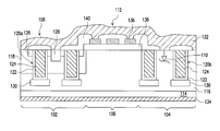
- FIG. 2 is a sectional view of FIG. 1 along a line A-A′.
- a monolithic MOSFET-Schottky diode device includes a chip 100 .
- the chip 100 is divided into a transistor region 102 , a diode region 104 and a termination region 106 .
- the transistor region 102 and the diode region 104 are divided by the termination region 106 , and the termination region 106 surrounds the transistor region 102 and the diode region 104 .
- a MOSFET 108 is an N-type trench MOSFET
- a Schottky diode 110 is a trench Schottky diode
- a termination structure 112 is a field plate structure.
- the MOSFETs 108 are disposed on the transistor region 102 .
- the Schottky diodes 110 are disposed on the diode region 104 .
- the termination structures 112 are disposed on the termination region 106 .
- the MOSFETs 108 are disposed on an N + -type substrate 114 .
- An N ⁇ -type doped region 116 is disposed on the N + -type substrate 114 .
- a P ⁇ -type doped region 118 is disposed on the N ⁇ -type doped region 116 .
- the MOFSET 108 includes a dielectric layer 122 disposed inside a groove 120 a , a conductive layer 124 served as a gate, and an N + -type source 126 .
- a material of the dielectric layer 122 may be, for example, silicon oxide.
- a material of the conductive layer 124 may be, for example, doped polycrystalline silicon.
- a P + -type doped region 128 is disposed between the N + -type sources 126 of two adjacent MOSFETs 108 .
- a conductive layer 132 contacts the P + -type doped region 128 .
- a material of the conductive layer 132 includes metal such as aluminum and copper.
- a P + -type doped region 130 may also be selectively disposed on a bottom portion of the groove 120 a .
- Another surface of the N + -type substrate 114 opposite to the MOSFET 108 is disposed with a conductive layer 134 .
- the conductive layer 134 is used as a drain of the MOSFET 108 .
- the same dielectric layer 122 and the conductive layer 124 filling groove 120 b is also disposed in the groove 120 b .
- the conductive layer 132 is disposed on the N + -type substrate 114 .
- the conductive layer 132 contacts the N ⁇ -type doped region 116 among the grooves 120 b , and is served as an anode of the Schottky diode 110 .
- the conductive layer 134 is disposed on another surface of the N + -type substrate 114 opposite to the Schottky diode 110 and is served as a cathode of the Schottky diode 110 .
- a bottom portion of the groove 120 b may also be selectively disposed with a P + -type doped region 130 .
- interlayer insulation layers 140 covering the conductive layers 124 or conductive layers 136 may be disposed on the N + -type substrate 114 .
- a field oxide layer 138 is formed on the N + -type substrate 114 .
- a material of the field oxide layer 138 may be, for example, silicon oxide.
- a plurality of conductive layers 136 are formed on the field oxide layer 138 .
- a material of the conductive layer 136 may be, for example, doped polycrystalline silicon.
- FIG. 3 is a sectional view of a flat MOSFET.
- the MOSFET in the monolithic MOSFET-Schottky diode device of the present invention may also be the flat MOSFET.
- a plurality of MOSFETs 208 are disposed on an N + -type substrate 214 .
- the N + -type substrate 214 is disposed with an N ⁇ -type doped region 216 .
- a P ⁇ -type doped region 218 is disposed in the N ⁇ -type doped region 216 .
- the MOSFET 208 includes a dielectric layer 222 disposed on the N + -type substrate 214 , a conductive layer 224 served as a gate, and an N + -type source 226 .
- a material of the dielectric layer 222 may be, for example, silicon oxide.
- a material of the conductive layer 224 may be, for example, doped polycrystalline silicon.
- a P + -type doped region 228 is disposed between the N + -type sources 226 of two adjacent MOSFETs 208 .
- a conductive layer 232 contacts the P + -type doped region 228 .
- a material of the conductive layer 232 includes metal such as aluminum and copper.
- Another surface of the N + -type substrate 214 opposite to the MOSFETs 208 is disposed with a conductive layer 234 .
- the conductive layer 234 is served as a drain of the MOSFET 208 .
- a material of the conductive layer 234 includes metal such as aluminum and copper.
- interlayer insulation layers 254 covering the conductive layers 224 are disposed on the N + -type substrate 114 .
- FIG. 4 is a sectional view of a junction barrier Schottky diode.
- the Schottky diode in the monolithic MOSFET-Schottky diode device of the present invention may also be the junction barrier Schottky diode.
- P + -type doped regions 240 are disposed in an N + -type substrate 214 .
- a conductive layer 232 is disposed on the N + -type substrate 214 .
- the conductive layer 232 contacts an N ⁇ -type doped region 216 among the P + -type doped regions 240 , and is served as an anode of the Schottky diode 210 .
- Another surface of the N + -type substrate 214 opposite to the Schottky diodes 210 is disposed with a conductive layer 234 .
- the conductive layer 234 is used to serve as a cathode of the Schottky diode 210 .
- FIG. 5 is a sectional view of another field plate structure.
- a termination structure of a monolithic MOSFET-Schottky diode device in the present invention may also be a field plate structure as shown in FIG. 5 .
- a plurality of field oxide layers 246 are formed on an N + -type substrate 214 .
- a material of the field oxide layer 246 is, for example, silicon oxide.
- a plurality of conductive layers 248 are respectively formed on the field oxide layer 246 .
- a material of the conductive layer 248 may be, for example, doped polycrystalline silicon.
- a P + -type doped region 250 is formed in an N ⁇ -type doped region 216 among the field oxide layers 246 .
- the P + -type doped region 250 and the conductive layers 248 connect the MOSFET and the Schottky diode through the conductive layer 252 .
- interlayer insulation layers 254 covering a part of the field oxide layers 246 and the conductive layers 248 are disposed on the N + -type substrate 214 .
- FIG. 6 is a sectional view of a guard ring structure.
- a termination structure of a monolithic MOSFET-Schottky diode device in the present invention may also be a guard ring structure.
- P + -type doped regions (guard rings) 242 are disposed in an N + -type substrate 214 .
- the P + -type doped regions 242 may surround the MOSFETs and the Schottky diodes for example.
- An insulation layer 244 is disposed on the N + -type substrate 214 .
- a material of the insulation layer 244 may be, for example, silicon oxide.
- the MOSFETs and the Schottky diodes only need to be integrated in a single chip; in addition, the MOSFETs and the Schottky diodes share the termination structures. Therefore, the MOSFETs, the Schottky diodes and the termination structures do not need to be limited. Instead, any combination of the MOSFETs, the Schottky diodes and the termination structures is allowed.
- the MOSFETs and the Schottky diodes are integrated in a single chip in the present invention; in addition, the MOSFETs and the Schottky diodes share the termination structures, therefore shrinking a device size, reducing a parasitic inductance value caused by bonding wires, reducing current surges and decreasing electromagnetic interference.
Abstract
Description
Claims (9)
Applications Claiming Priority (3)
| Application Number | Priority Date | Filing Date | Title |
|---|---|---|---|
| TW100117791A | 2011-05-20 | ||
| TW100117791 | 2011-05-20 | ||
| TW100117791A TW201248854A (en) | 2011-05-20 | 2011-05-20 | Monolithic metal oxide semiconductor field effect transistors with schottky diode device |
Publications (2)
| Publication Number | Publication Date |
|---|---|
| US20120292695A1 US20120292695A1 (en) | 2012-11-22 |
| US8669614B2 true US8669614B2 (en) | 2014-03-11 |
Family
ID=47174311
Family Applications (1)
| Application Number | Title | Priority Date | Filing Date |
|---|---|---|---|
| US13/349,572 Expired - Fee Related US8669614B2 (en) | 2011-05-20 | 2012-01-13 | Monolithic metal oxide semiconductor field effect transistor-Schottky diode device |
Country Status (2)
| Country | Link |
|---|---|
| US (1) | US8669614B2 (en) |
| TW (1) | TW201248854A (en) |
Cited By (6)
| Publication number | Priority date | Publication date | Assignee | Title |
|---|---|---|---|---|
| US9614043B2 (en) | 2012-02-09 | 2017-04-04 | Vishay-Siliconix | MOSFET termination trench |
| US9842911B2 (en) | 2012-05-30 | 2017-12-12 | Vishay-Siliconix | Adaptive charge balanced edge termination |
| US9882044B2 (en) | 2014-08-19 | 2018-01-30 | Vishay-Siliconix | Edge termination for super-junction MOSFETs |
| US9887259B2 (en) | 2014-06-23 | 2018-02-06 | Vishay-Siliconix | Modulated super junction power MOSFET devices |
| US10084079B2 (en) | 2015-06-16 | 2018-09-25 | Samsung Electronics Co., Ltd. | Semiconductor device having a drift region with non-uniform impurity concentration profile |
| US11031472B2 (en) | 2018-12-28 | 2021-06-08 | General Electric Company | Systems and methods for integrated diode field-effect transistor semiconductor devices |
Citations (5)
| Publication number | Priority date | Publication date | Assignee | Title |
|---|---|---|---|---|
| US6351018B1 (en) | 1999-02-26 | 2002-02-26 | Fairchild Semiconductor Corporation | Monolithically integrated trench MOSFET and Schottky diode |
| US6433396B1 (en) | 1999-10-05 | 2002-08-13 | International Rectifier Corporation | Trench MOSFET with integrated schottky device and process for its manufacture |
| US20090315107A1 (en) | 2008-06-23 | 2009-12-24 | Force Mos Technology Co. Ltd. | Integrated trench mosfet and junction barrier schottky rectifier with trench contact structures |
| US20100176446A1 (en) | 2009-01-13 | 2010-07-15 | Force Mos Technology Co. Ltd. | MOSFET with source contact in trench and integrated schottky diode |
| US8222678B2 (en) * | 2009-08-17 | 2012-07-17 | Excelliance Mos Corporation | Semiconductor structure |
-
2011
- 2011-05-20 TW TW100117791A patent/TW201248854A/en unknown
-
2012
- 2012-01-13 US US13/349,572 patent/US8669614B2/en not_active Expired - Fee Related
Patent Citations (5)
| Publication number | Priority date | Publication date | Assignee | Title |
|---|---|---|---|---|
| US6351018B1 (en) | 1999-02-26 | 2002-02-26 | Fairchild Semiconductor Corporation | Monolithically integrated trench MOSFET and Schottky diode |
| US6433396B1 (en) | 1999-10-05 | 2002-08-13 | International Rectifier Corporation | Trench MOSFET with integrated schottky device and process for its manufacture |
| US20090315107A1 (en) | 2008-06-23 | 2009-12-24 | Force Mos Technology Co. Ltd. | Integrated trench mosfet and junction barrier schottky rectifier with trench contact structures |
| US20100176446A1 (en) | 2009-01-13 | 2010-07-15 | Force Mos Technology Co. Ltd. | MOSFET with source contact in trench and integrated schottky diode |
| US8222678B2 (en) * | 2009-08-17 | 2012-07-17 | Excelliance Mos Corporation | Semiconductor structure |
Cited By (10)
| Publication number | Priority date | Publication date | Assignee | Title |
|---|---|---|---|---|
| US9614043B2 (en) | 2012-02-09 | 2017-04-04 | Vishay-Siliconix | MOSFET termination trench |
| US9935193B2 (en) | 2012-02-09 | 2018-04-03 | Siliconix Technology C. V. | MOSFET termination trench |
| US9842911B2 (en) | 2012-05-30 | 2017-12-12 | Vishay-Siliconix | Adaptive charge balanced edge termination |
| US10229988B2 (en) | 2012-05-30 | 2019-03-12 | Vishay-Siliconix | Adaptive charge balanced edge termination |
| US9887259B2 (en) | 2014-06-23 | 2018-02-06 | Vishay-Siliconix | Modulated super junction power MOSFET devices |
| US10283587B2 (en) | 2014-06-23 | 2019-05-07 | Vishay-Siliconix | Modulated super junction power MOSFET devices |
| US9882044B2 (en) | 2014-08-19 | 2018-01-30 | Vishay-Siliconix | Edge termination for super-junction MOSFETs |
| US10340377B2 (en) | 2014-08-19 | 2019-07-02 | Vishay-Siliconix | Edge termination for super-junction MOSFETs |
| US10084079B2 (en) | 2015-06-16 | 2018-09-25 | Samsung Electronics Co., Ltd. | Semiconductor device having a drift region with non-uniform impurity concentration profile |
| US11031472B2 (en) | 2018-12-28 | 2021-06-08 | General Electric Company | Systems and methods for integrated diode field-effect transistor semiconductor devices |
Also Published As
| Publication number | Publication date |
|---|---|
| TW201248854A (en) | 2012-12-01 |
| US20120292695A1 (en) | 2012-11-22 |
Similar Documents
| Publication | Publication Date | Title |
|---|---|---|
| US6707128B2 (en) | Vertical MISFET transistor surrounded by a Schottky barrier diode with a common source and anode electrode | |
| US11557587B2 (en) | Semiconductor device and semiconductor package | |
| US10388781B2 (en) | Device structure having inter-digitated back to back MOSFETs | |
| US9368617B2 (en) | Superjunction device and semiconductor structure comprising the same | |
| US8669614B2 (en) | Monolithic metal oxide semiconductor field effect transistor-Schottky diode device | |
| US9437728B2 (en) | Semiconductor device | |
| US20020179945A1 (en) | Power semiconductor device | |
| US9209293B2 (en) | Integrated device having MOSFET cell array embedded with barrier Schottky diode | |
| US10249759B2 (en) | Connection arrangements for integrated lateral diffusion field effect transistors | |
| JP6000513B2 (en) | Insulated gate semiconductor device | |
| US8319284B2 (en) | Laterally diffused metal-oxide-semiconductor device | |
| US11335627B2 (en) | Connection arrangements for integrated lateral diffusion field effect transistors having a backside contact | |
| US20130168767A1 (en) | Lateral Diffused Metal-Oxide-Semiconductor Device | |
| US7888733B2 (en) | Power semiconductor device | |
| US20140117424A1 (en) | Semiconductor device | |
| JP2009071059A (en) | Semiconductor device | |
| JP2023022141A (en) | Semiconductor device and power module | |
| WO2016185544A1 (en) | Semiconductor device and power conversion device | |
| CN103681669B (en) | Public drain electrode power supply folder for battery pack protection MOSFET | |
| JP5338448B2 (en) | Semiconductor device | |
| CN102800670A (en) | One-chip type metal-oxide semiconductor field effect transistor-Schottky diode element | |
| CN113410200A (en) | Chip packaging frame and chip packaging structure |
Legal Events
| Date | Code | Title | Description |
|---|---|---|---|
| AS | Assignment |
Owner name: BEYOND INNOVATION TECHNOLOGY CO., LTD., TAIWAN Free format text: ASSIGNMENT OF ASSIGNORS INTEREST;ASSIGNOR:CHENG, CHIEN-HSING;REEL/FRAME:027538/0958 Effective date: 20120106 |
|
| STCF | Information on status: patent grant |
Free format text: PATENTED CASE |
|
| MAFP | Maintenance fee payment |
Free format text: PAYMENT OF MAINTENANCE FEE, 4TH YR, SMALL ENTITY (ORIGINAL EVENT CODE: M2551) Year of fee payment: 4 |
|
| FEPP | Fee payment procedure |
Free format text: MAINTENANCE FEE REMINDER MAILED (ORIGINAL EVENT CODE: REM.); ENTITY STATUS OF PATENT OWNER: SMALL ENTITY |
|
| LAPS | Lapse for failure to pay maintenance fees |
Free format text: PATENT EXPIRED FOR FAILURE TO PAY MAINTENANCE FEES (ORIGINAL EVENT CODE: EXP.); ENTITY STATUS OF PATENT OWNER: SMALL ENTITY |
|
| STCH | Information on status: patent discontinuation |
Free format text: PATENT EXPIRED DUE TO NONPAYMENT OF MAINTENANCE FEES UNDER 37 CFR 1.362 |
|
| FP | Lapsed due to failure to pay maintenance fee |
Effective date: 20220311 |