US8716111B2 - Method for manufacturing trench type superjunction device and trench type superjunction device - Google Patents
Method for manufacturing trench type superjunction device and trench type superjunction device Download PDFInfo
- Publication number
- US8716111B2 US8716111B2 US13/167,450 US201113167450A US8716111B2 US 8716111 B2 US8716111 B2 US 8716111B2 US 201113167450 A US201113167450 A US 201113167450A US 8716111 B2 US8716111 B2 US 8716111B2
- Authority
- US
- United States
- Prior art keywords
- type
- trench
- layer
- implantation
- ion implantation
- Prior art date
- Legal status (The legal status is an assumption and is not a legal conclusion. Google has not performed a legal analysis and makes no representation as to the accuracy of the status listed.)
- Active, expires
Links
- 238000000034 method Methods 0.000 title claims abstract description 48
- 238000004519 manufacturing process Methods 0.000 title claims abstract description 13
- 238000002513 implantation Methods 0.000 claims abstract description 41
- XUIMIQQOPSSXEZ-UHFFFAOYSA-N Silicon Chemical compound [Si] XUIMIQQOPSSXEZ-UHFFFAOYSA-N 0.000 claims abstract description 27
- 229910052710 silicon Inorganic materials 0.000 claims abstract description 27
- 239000010703 silicon Substances 0.000 claims abstract description 27
- 239000012535 impurity Substances 0.000 claims description 28
- 239000007943 implant Substances 0.000 claims description 25
- 239000004065 semiconductor Substances 0.000 claims description 20
- 238000005468 ion implantation Methods 0.000 claims description 17
- 239000000758 substrate Substances 0.000 claims description 16
- 239000005380 borophosphosilicate glass Substances 0.000 claims description 6
- VYPSYNLAJGMNEJ-UHFFFAOYSA-N Silicium dioxide Chemical compound O=[Si]=O VYPSYNLAJGMNEJ-UHFFFAOYSA-N 0.000 claims description 4
- 229910052814 silicon oxide Inorganic materials 0.000 claims description 4
- 238000005229 chemical vapour deposition Methods 0.000 claims description 3
- 238000005498 polishing Methods 0.000 claims description 3
- 239000000126 substance Substances 0.000 claims description 3
- 229910021417 amorphous silicon Inorganic materials 0.000 claims description 2
- 238000000151 deposition Methods 0.000 claims 1
- 230000003647 oxidation Effects 0.000 claims 1
- 238000007254 oxidation reaction Methods 0.000 claims 1
- 230000015556 catabolic process Effects 0.000 abstract description 11
- 239000010410 layer Substances 0.000 description 64
- 238000005530 etching Methods 0.000 description 6
- 229920002120 photoresistant polymer Polymers 0.000 description 4
- 229910021420 polycrystalline silicon Inorganic materials 0.000 description 4
- 229920005591 polysilicon Polymers 0.000 description 4
- 230000012010 growth Effects 0.000 description 3
- 239000002184 metal Substances 0.000 description 3
- 238000004088 simulation Methods 0.000 description 3
- ZOXJGFHDIHLPTG-UHFFFAOYSA-N Boron Chemical compound [B] ZOXJGFHDIHLPTG-UHFFFAOYSA-N 0.000 description 2
- 229910052796 boron Inorganic materials 0.000 description 2
- 230000015572 biosynthetic process Effects 0.000 description 1
- 238000009792 diffusion process Methods 0.000 description 1
- 238000009826 distribution Methods 0.000 description 1
- 230000005684 electric field Effects 0.000 description 1
- 239000011229 interlayer Substances 0.000 description 1
- 239000000463 material Substances 0.000 description 1
- 229910044991 metal oxide Inorganic materials 0.000 description 1
- 150000004706 metal oxides Chemical class 0.000 description 1
- 238000012986 modification Methods 0.000 description 1
- 230000004048 modification Effects 0.000 description 1
- 239000011800 void material Substances 0.000 description 1
Images


Classifications
-
- H—ELECTRICITY
- H01—ELECTRIC ELEMENTS
- H01L—SEMICONDUCTOR DEVICES NOT COVERED BY CLASS H10
- H01L21/00—Processes or apparatus adapted for the manufacture or treatment of semiconductor or solid state devices or of parts thereof
- H01L21/02—Manufacture or treatment of semiconductor devices or of parts thereof
- H01L21/04—Manufacture or treatment of semiconductor devices or of parts thereof the devices having at least one potential-jump barrier or surface barrier, e.g. PN junction, depletion layer or carrier concentration layer
- H01L21/18—Manufacture or treatment of semiconductor devices or of parts thereof the devices having at least one potential-jump barrier or surface barrier, e.g. PN junction, depletion layer or carrier concentration layer the devices having semiconductor bodies comprising elements of Group IV of the Periodic System or AIIIBV compounds with or without impurities, e.g. doping materials
- H01L21/26—Bombardment with radiation
- H01L21/263—Bombardment with radiation with high-energy radiation
- H01L21/265—Bombardment with radiation with high-energy radiation producing ion implantation
- H01L21/26506—Bombardment with radiation with high-energy radiation producing ion implantation in group IV semiconductors
- H01L21/26513—Bombardment with radiation with high-energy radiation producing ion implantation in group IV semiconductors of electrically active species
-
- H—ELECTRICITY
- H01—ELECTRIC ELEMENTS
- H01L—SEMICONDUCTOR DEVICES NOT COVERED BY CLASS H10
- H01L29/00—Semiconductor devices adapted for rectifying, amplifying, oscillating or switching, or capacitors or resistors with at least one potential-jump barrier or surface barrier, e.g. PN junction depletion layer or carrier concentration layer; Details of semiconductor bodies or of electrodes thereof ; Multistep manufacturing processes therefor
- H01L29/02—Semiconductor bodies ; Multistep manufacturing processes therefor
- H01L29/06—Semiconductor bodies ; Multistep manufacturing processes therefor characterised by their shape; characterised by the shapes, relative sizes, or dispositions of the semiconductor regions ; characterised by the concentration or distribution of impurities within semiconductor regions
- H01L29/0603—Semiconductor bodies ; Multistep manufacturing processes therefor characterised by their shape; characterised by the shapes, relative sizes, or dispositions of the semiconductor regions ; characterised by the concentration or distribution of impurities within semiconductor regions characterised by particular constructional design considerations, e.g. for preventing surface leakage, for controlling electric field concentration or for internal isolations regions
- H01L29/0607—Semiconductor bodies ; Multistep manufacturing processes therefor characterised by their shape; characterised by the shapes, relative sizes, or dispositions of the semiconductor regions ; characterised by the concentration or distribution of impurities within semiconductor regions characterised by particular constructional design considerations, e.g. for preventing surface leakage, for controlling electric field concentration or for internal isolations regions for preventing surface leakage or controlling electric field concentration
- H01L29/0611—Semiconductor bodies ; Multistep manufacturing processes therefor characterised by their shape; characterised by the shapes, relative sizes, or dispositions of the semiconductor regions ; characterised by the concentration or distribution of impurities within semiconductor regions characterised by particular constructional design considerations, e.g. for preventing surface leakage, for controlling electric field concentration or for internal isolations regions for preventing surface leakage or controlling electric field concentration for increasing or controlling the breakdown voltage of reverse biased devices
- H01L29/0615—Semiconductor bodies ; Multistep manufacturing processes therefor characterised by their shape; characterised by the shapes, relative sizes, or dispositions of the semiconductor regions ; characterised by the concentration or distribution of impurities within semiconductor regions characterised by particular constructional design considerations, e.g. for preventing surface leakage, for controlling electric field concentration or for internal isolations regions for preventing surface leakage or controlling electric field concentration for increasing or controlling the breakdown voltage of reverse biased devices by the doping profile or the shape or the arrangement of the PN junction, or with supplementary regions, e.g. junction termination extension [JTE]
- H01L29/063—Reduced surface field [RESURF] pn-junction structures
- H01L29/0634—Multiple reduced surface field (multi-RESURF) structures, e.g. double RESURF, charge compensation, cool, superjunction (SJ), 3D-RESURF, composite buffer (CB) structures
-
- H—ELECTRICITY
- H01—ELECTRIC ELEMENTS
- H01L—SEMICONDUCTOR DEVICES NOT COVERED BY CLASS H10
- H01L29/00—Semiconductor devices adapted for rectifying, amplifying, oscillating or switching, or capacitors or resistors with at least one potential-jump barrier or surface barrier, e.g. PN junction depletion layer or carrier concentration layer; Details of semiconductor bodies or of electrodes thereof ; Multistep manufacturing processes therefor
- H01L29/66—Types of semiconductor device ; Multistep manufacturing processes therefor
- H01L29/66007—Multistep manufacturing processes
- H01L29/66075—Multistep manufacturing processes of devices having semiconductor bodies comprising group 14 or group 13/15 materials
- H01L29/66227—Multistep manufacturing processes of devices having semiconductor bodies comprising group 14 or group 13/15 materials the devices being controllable only by the electric current supplied or the electric potential applied, to an electrode which does not carry the current to be rectified, amplified or switched, e.g. three-terminal devices
- H01L29/66409—Unipolar field-effect transistors
- H01L29/66477—Unipolar field-effect transistors with an insulated gate, i.e. MISFET
- H01L29/66674—DMOS transistors, i.e. MISFETs with a channel accommodating body or base region adjoining a drain drift region
- H01L29/66712—Vertical DMOS transistors, i.e. VDMOS transistors
-
- H—ELECTRICITY
- H01—ELECTRIC ELEMENTS
- H01L—SEMICONDUCTOR DEVICES NOT COVERED BY CLASS H10
- H01L29/00—Semiconductor devices adapted for rectifying, amplifying, oscillating or switching, or capacitors or resistors with at least one potential-jump barrier or surface barrier, e.g. PN junction depletion layer or carrier concentration layer; Details of semiconductor bodies or of electrodes thereof ; Multistep manufacturing processes therefor
- H01L29/66—Types of semiconductor device ; Multistep manufacturing processes therefor
- H01L29/68—Types of semiconductor device ; Multistep manufacturing processes therefor controllable by only the electric current supplied, or only the electric potential applied, to an electrode which does not carry the current to be rectified, amplified or switched
- H01L29/76—Unipolar devices, e.g. field effect transistors
- H01L29/772—Field effect transistors
- H01L29/78—Field effect transistors with field effect produced by an insulated gate
- H01L29/7801—DMOS transistors, i.e. MISFETs with a channel accommodating body or base region adjoining a drain drift region
- H01L29/7802—Vertical DMOS transistors, i.e. VDMOS transistors
- H01L29/7811—Vertical DMOS transistors, i.e. VDMOS transistors with an edge termination structure
-
- H—ELECTRICITY
- H01—ELECTRIC ELEMENTS
- H01L—SEMICONDUCTOR DEVICES NOT COVERED BY CLASS H10
- H01L21/00—Processes or apparatus adapted for the manufacture or treatment of semiconductor or solid state devices or of parts thereof
- H01L21/02—Manufacture or treatment of semiconductor devices or of parts thereof
- H01L21/04—Manufacture or treatment of semiconductor devices or of parts thereof the devices having at least one potential-jump barrier or surface barrier, e.g. PN junction, depletion layer or carrier concentration layer
- H01L21/18—Manufacture or treatment of semiconductor devices or of parts thereof the devices having at least one potential-jump barrier or surface barrier, e.g. PN junction, depletion layer or carrier concentration layer the devices having semiconductor bodies comprising elements of Group IV of the Periodic System or AIIIBV compounds with or without impurities, e.g. doping materials
- H01L21/26—Bombardment with radiation
- H01L21/263—Bombardment with radiation with high-energy radiation
- H01L21/265—Bombardment with radiation with high-energy radiation producing ion implantation
- H01L21/2658—Bombardment with radiation with high-energy radiation producing ion implantation of a molecular ion, e.g. decaborane
-
- H—ELECTRICITY
- H01—ELECTRIC ELEMENTS
- H01L—SEMICONDUCTOR DEVICES NOT COVERED BY CLASS H10
- H01L21/00—Processes or apparatus adapted for the manufacture or treatment of semiconductor or solid state devices or of parts thereof
- H01L21/02—Manufacture or treatment of semiconductor devices or of parts thereof
- H01L21/04—Manufacture or treatment of semiconductor devices or of parts thereof the devices having at least one potential-jump barrier or surface barrier, e.g. PN junction, depletion layer or carrier concentration layer
- H01L21/18—Manufacture or treatment of semiconductor devices or of parts thereof the devices having at least one potential-jump barrier or surface barrier, e.g. PN junction, depletion layer or carrier concentration layer the devices having semiconductor bodies comprising elements of Group IV of the Periodic System or AIIIBV compounds with or without impurities, e.g. doping materials
- H01L21/26—Bombardment with radiation
- H01L21/263—Bombardment with radiation with high-energy radiation
- H01L21/265—Bombardment with radiation with high-energy radiation producing ion implantation
- H01L21/26586—Bombardment with radiation with high-energy radiation producing ion implantation characterised by the angle between the ion beam and the crystal planes or the main crystal surface
-
- H—ELECTRICITY
- H01—ELECTRIC ELEMENTS
- H01L—SEMICONDUCTOR DEVICES NOT COVERED BY CLASS H10
- H01L29/00—Semiconductor devices adapted for rectifying, amplifying, oscillating or switching, or capacitors or resistors with at least one potential-jump barrier or surface barrier, e.g. PN junction depletion layer or carrier concentration layer; Details of semiconductor bodies or of electrodes thereof ; Multistep manufacturing processes therefor
- H01L29/02—Semiconductor bodies ; Multistep manufacturing processes therefor
- H01L29/06—Semiconductor bodies ; Multistep manufacturing processes therefor characterised by their shape; characterised by the shapes, relative sizes, or dispositions of the semiconductor regions ; characterised by the concentration or distribution of impurities within semiconductor regions
- H01L29/10—Semiconductor bodies ; Multistep manufacturing processes therefor characterised by their shape; characterised by the shapes, relative sizes, or dispositions of the semiconductor regions ; characterised by the concentration or distribution of impurities within semiconductor regions with semiconductor regions connected to an electrode not carrying current to be rectified, amplified or switched and such electrode being part of a semiconductor device which comprises three or more electrodes
- H01L29/1095—Body region, i.e. base region, of DMOS transistors or IGBTs
Definitions
- the present invention relates to a trench type super junction device and its manufacturing method.
- a super junction structure adopts an alternating P type and N type structure to replace the N drift region of a traditional VDMOS (Vertical Double-Diffused Metal Oxide Semiconductor).
- VDMOS Very Double-Diffused Metal Oxide Semiconductor
- the super junction structure can be applied to the fabrication of a MOSFET so as to manufacture a super junction MOSFET. Since a super junction MOSFET adopts a low resistance epitaxial layer, a much lower on resistance can be achieved while maintaining a same breakdown voltage as a traditional VDMOS.
- the deep trench should have a depth equal or nearly equal with the thickness of the epitaxial layer in which the deep trench is formed; besides, the profile of the deep trench should be vertical so as to make sure that the silicon filled in the deep trench has a good uniformity of concentration.
- CMP process is used to planarize the surface of the deep trenches, so that an alternating P type and N type structure is finished.
- the problem is that the process of deep trench etching and tilling is very difficult to control, and the manufacturing cost is very high.
- An object of the present invention is to provide a trench type super junction device to improve the breakdown voltage of a high-voltage super junction MOSFET, and reduce the difficulty of the process of forming deep trenches.
- the present invention provides a method for manufacturing trench type super junction device, which includes:
- the present invention further provides a trench type super junction device manufactured by using the above-mentioned method, wherein the device comprises alternating P type and N type thin layers; the P type thin layer is formed by the P type semiconductor layer filled in the trench and the one or more P type implantation regions below the trench; the N type thin layer is formed by the N type epitaxial layer.
- the present invention has the advantages that: the epitaxial layer between the bottom of the trench and the substrate is better depleted by adding one or more implantation regions below the trench, thus improving the breakdown voltage of the device; the difficulty of trench etching process is reduced as shallower trenches and slightly oblique trench profiles are acceptable in the present invention.
- FIG. 1A ?? FIG. 1 C are sectional views of the method for manufacturing trench type super junction device according to a first embodiment of the present invention.
- FIG. 2 is a schematic view of the impurities implanted below the bottom of the trenches according to a second embodiment of the present invention.
- FIG. 3 is a schematic view of the impurities implanted below the bottom of the trenches according to a third embodiment of the present invention.
- FIG. 4 is a schematic view of the impurities implanted below the bottom of the trenches according to a fourth embodiment of the present invention.
- FIG. 5 ⁇ FIG . 6 are schematic views of the materials filled in the trenches according to the present invention.
- FIG. 7 is a sectional view of the trench type super junction device according to the present invention.
- FIG. 8 shows simulation results of an NMOS according to the present invention.
- the method for manufacturing trench type super junction device includes the following steps:
- Step 1 firstly form an N ⁇ epitaxial layer 2 on an N+ silicon substrate 1 , wherein the Rs (Resistivity) of the N+ substrate 1 is in a range of 0.001 ⁇ 0.003 ⁇ cm; the thickness and the Rs of the N ⁇ epitaxial layer 2 are determined according to the design requirement of the device. For a device of 600V BVDS (breakdown voltage), the Rs of the N ⁇ epitaxial layer 2 is 2 ⁇ 10 ⁇ cm, and the thickness of the N ⁇ epitaxial layer 2 is 40 ⁇ 55 ⁇ m.
- the dielectric film 31 can be a silicon oxide film, and the dielectric film 31 can be used as hard mask during the subsequent process of trench etching and can also be used as stop layer during the subsequent process of chemical mechanical polishing.
- trenches 3 in the N ⁇ epitaxial layer 2 by photolithograph and etch, wherein the trenches 3 may be formed in the N ⁇ epitaxial layer 2 without reaching the N+ substrate 1 (as shown in FIG. 1A ); or the bottom of the trenches 3 may just reach the interface of the N ⁇ epitaxial layer 2 and the N+ substrate 1 ; or the trenches 3 may be etched through the N ⁇ epitaxial layer 2 into the N+ substrate 1 .
- the depth of the trenches 3 is depended on the design requirement of the device.
- the dielectric film 31 can be formed by thermal oxide process, or by chemical vapor deposition (CVD) process. During the process of trench etching, the dielectric film 31 can be used as hard mask, or a photoresist layer (not shown in the figure) may be used as hard mask by adopting the following steps after the formation of the dielectric film 31 : deposit a photoresist layer on the dielectric film; form one or more etch windows in the photoresist layer by exposure and development; etch the dielectric film 31 and the N ⁇ epitaxial layer 2 in the etch windows by using the photoresist layer as hard mask to form trenches in the N ⁇ epitaxial layer.
- the remaining dielectric film after trench etching should preferably have a thickness of more than 1000 ⁇ .
- Step 2 as shown in FIG. 1B , form one or more P type implantation regions 4 below each of the trenches 3 by P type ion implantation.
- the P type impurity concentration is in a range of 1E15 ⁇ 10E15/cm 3 .
- only one P type implantation region 4 is formed below each trench 3 , and the implantation region 4 is connected with the bottom of the trench 3 .
- Step 3 fill each trench with a P type semiconductor layer 5 , wherein the P type semiconductor layer 5 is formed by a P type silicon layer (see FIG. 1C ), or by a combination of a P type silicon layer 51 and a none-doped silicon layer 52 (see FIG. 5 ), or by a combination of a P type silicon layer 51 and a dielectric layer 53 (see FIG. 6 ); then remove the P type semiconductor layer 5 above the surface of the dielectric film 31 by CMP process or etch back process; afterwards, remove the dielectric film 31 .
- the P type semiconductor layer 5 is formed by a P type silicon layer (see FIG. 1C ), or by a combination of a P type silicon layer 51 and a none-doped silicon layer 52 (see FIG. 5 ), or by a combination of a P type silicon layer 51 and a dielectric layer 53 (see FIG. 6 ); then remove the P type semiconductor layer 5 above the surface of the dielectric film 31 by CMP process or etch back process; afterwards, remove the dielectric film 31
- the impurities in the P type semiconductor layer 5 filled in the trenches and the impurities in the P type implantation regions 4 are used together to keep balance with the N type impurities in the N ⁇ epitaxial layer 2 .
- the total quantity of P type impurities in the implantation regions 4 and the P type semiconductor layer 5 shall he equal with the total quantity of N type impurities in the N ⁇ epitaxial layer 2 to get an ideal device character.
- FIG. 2 shows a schematic view of the impurities implanted below the bottom of the trenches according to a second embodiment of the present invention.
- a P type implantation region 4 is formed below the bottom of each trench 3 , while the P type implantation region 4 is not connected with the bottom of the trench 3 .
- the structure as shown in FIG. 2 can be formed by performing a single step of P type ion implantation, while the depth of P type ion implantation is greater than the depth of the trenches 3 .
- FIG. 3 shows a schematic view of the impurities implanted below the bottom of the trenches according to a third embodiment of the present invention.
- more than one P type implantation regions 4 are formed below the bottom of each trench 3 ; the P type implantation regions 4 are connected with one another, and the P type implantation region closest to the trench is connected with the bottom of the trench 3 .
- the structure as shown in FIG. 3 can be formed by performing multiple steps of P type ion implantation with different implant energies. The implant energies are controlled such that the P type implantation regions 4 below each trench are consecutive in a vertical direction.
- FIG. 4 shows a schematic view of the impurities implanted below the bottom of the trenches according to a fourth embodiment of the present invention.
- more than one P type implantation regions 4 are formed below the bottom of each trench 3 ; the P type implantation regions 4 are not connected with one another, and the P type implantation region closest to the trench is not connected with the bottom of the trench 3 .
- the structure as shown in FIG. 4 can be formed by performing multiple steps of P type ion implantation with different implant energies. The implant energies are controlled such that the P type implantation regions 4 below each trench are not consecutive in the vertical direction.
- the one or more P type implantation regions 4 below each trench 3 may connect or disconnect with the bottom of the trench 3 , and may connect or disconnect with the N+ substrate 1 .
- the P type silicon layer can be made of monocrystal silicon, polycrystal silicon or amorphous silicon; the growth temperature of P type silicon layer may be in a range of 650 ⁇ 1200.
- the P type semiconductor layer 5 filled in the trenches is formed by a combination of a P type silicon layer 51 and a none-doped silicon layer 52 , the P type silicon layer 51 is deposited first, and followed by the none-doped silicon layer 52 ; the growth temperature of none-doped silicon layer 52 may be in a range of 510 ⁇ 650. As shown in FIG.
- the dielectric layer 53 can be selected from non-doped silicon oxide layer or BPSG (borophosphosilicate glass).
- the dielectric layer 53 is selected according to the requirement of trench filling time and the permissibility of voids in the trench.
- BPSG is preferably used to achieve non-void trench filling.
- a P type silicon layer can be deposited in the trench first, and followed by a BPSG dielectric layer. Due to the reflow property of the BPSG layer, the voids in the trench can be easily filled during a thermal process.
- VDMOS vertical double-diffusion metal-oxide-semiconductor
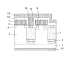
- further steps are taken to produce a complete super junction NMOS device, including: form gate oxide layer 6 and polysilicon gates 7 on the P ⁇ epitaxial layer 2 ; form P wells 8 and N+ layers 9 ; form an inter layer dielectric film 10 on the polysilicon gates 7 to isolate polysilicon from metal; form contact holes 11 and P+ ohmic contact regions 12 ; form source metal electrodes 13 and gate polysilicon electrodes (not shown in the figure); form drain electrode (backside metal) 14 at the backside of the N+ substrate 1 .
- VDMOS vertical double-diffusion metal-oxide-semiconductor
- the profile of the trenches according to the present invention can be vertical (90 degree) with regard to the surface of the substrate, or oblique (not strictly vertical).
- the bottom shape of the trenches can be flat or curved.
- FIG. 8 a simulation is made to compare the breakdown voltages of a conventional NMOS having no impurities implanted below the trenches (see FIG. 8( a )) and a super junction NMOS with oblique trench profiles and P type implantation regions below the trenches according to the present invention (see FIG.
- the distance from the bottom of the trenches to the surface of the substrate is about 7 ⁇ 10 ⁇ m; the P type implantation regions are formed by using boron as impurity with an implant energy of 100 Kev and an implant dose of 5E12/cm 2 .
- the simulation result shows that the breakdown voltage of the conventional NMOS is only 610V while the breakdown voltage of the NMOS according to the present invention is 680V. As shown in FIGS.
- the implantation step with the highest implant energy can be performed first, the lowest last; or the lowest first and the highest last.
- the implant energy can be in a range of 0.5 kev to 10000 kev or even higher or lower.
- the implant energy is determined by the ability of the implant equipment. The higher the implant energy is, the greater depth the implantation region can reach, so that the trenches could be formed shallower, thus reducing the difficulty in trench etching process. In case that high implant energy is not available, the breakdown voltage of the NMOS may still be improved by implanting some P type impurities near the bottom of the trenches.
- the impurities adopted in the P type implantation steps can be boron (B), BF2, or other impurities; the implant angle can be in a range of 0 ⁇ 10 degrees; the implant dose of the P type impurities can be in a range of 1E11 ⁇ 1E14/cm 2 , determined by device requirement.
- the impurity concentration of the P type implantation regions is of the same order of magnitude with the impurity concentration of the P type semiconductor layer filled in the trenches.
Abstract
Description
Claims (18)
Applications Claiming Priority (3)
| Application Number | Priority Date | Filing Date | Title |
|---|---|---|---|
| CN2010102087463A CN102299072A (en) | 2010-06-24 | 2010-06-24 | Grooved super-junction device and method for manufacturing grooved super-junction device |
| CN201010208746 | 2010-06-24 | ||
| CN201010208746.3 | 2010-06-24 |
Publications (2)
| Publication Number | Publication Date |
|---|---|
| US20110316121A1 US20110316121A1 (en) | 2011-12-29 |
| US8716111B2 true US8716111B2 (en) | 2014-05-06 |
Family
ID=45351736
Family Applications (1)
| Application Number | Title | Priority Date | Filing Date |
|---|---|---|---|
| US13/167,450 Active 2033-01-01 US8716111B2 (en) | 2010-06-24 | 2011-06-23 | Method for manufacturing trench type superjunction device and trench type superjunction device |
Country Status (2)
| Country | Link |
|---|---|
| US (1) | US8716111B2 (en) |
| CN (1) | CN102299072A (en) |
Cited By (1)
| Publication number | Priority date | Publication date | Assignee | Title |
|---|---|---|---|---|
| US20130175608A1 (en) * | 2012-01-11 | 2013-07-11 | Tsung-Hsiung LEE | Semiconductor device and fabricating method thereof |
Families Citing this family (11)
| Publication number | Priority date | Publication date | Assignee | Title |
|---|---|---|---|---|
| CN103208512B (en) * | 2012-01-17 | 2016-11-16 | 上海华虹宏力半导体制造有限公司 | The nmos switch device of low source-and-drain junction electric capacity and manufacture method thereof |
| US8901641B2 (en) * | 2012-02-01 | 2014-12-02 | Vanguard International Semiconductor Corporation | Semiconductor device with super junction structure and method for fabricating the same |
| US20130307058A1 (en) * | 2012-05-18 | 2013-11-21 | Infineon Technologies Austria Ag | Semiconductor Devices Including Superjunction Structure and Method of Manufacturing |
| CN103633137A (en) * | 2012-08-21 | 2014-03-12 | 朱江 | A semiconductor wafer with a bottom isolation charge compensation structure and a manufacturing method thereof |
| CN103050523B (en) * | 2012-12-14 | 2015-10-14 | 上海华虹宏力半导体制造有限公司 | Insulated gate bipolar transistor and manufacture method thereof |
| WO2015100525A1 (en) * | 2013-12-30 | 2015-07-09 | 电子科技大学 | Method for fabricating a power semiconductor device longitudinal superjunction drift region structure |
| US9852902B2 (en) * | 2014-10-03 | 2017-12-26 | Applied Materials, Inc. | Material deposition for high aspect ratio structures |
| CN104779295B (en) * | 2015-04-24 | 2018-11-06 | 无锡同方微电子有限公司 | Half super node MOSFET structure of one kind and preparation method thereof |
| DE102015109545B4 (en) * | 2015-06-15 | 2021-10-21 | Infineon Technologies Ag | Transistor with field electrodes and improved avalanche breakdown behavior |
| CN111370305A (en) * | 2020-04-30 | 2020-07-03 | 上海华虹宏力半导体制造有限公司 | Deep groove type super junction device and manufacturing method thereof |
| CN113299739A (en) * | 2021-05-21 | 2021-08-24 | 江苏东海半导体科技有限公司 | Power device epitaxial structure and manufacturing method thereof |
Citations (7)
| Publication number | Priority date | Publication date | Assignee | Title |
|---|---|---|---|---|
| US20040129973A1 (en) | 2003-01-07 | 2004-07-08 | Wataru Saito | Power semiconductor device |
| US20070013000A1 (en) | 2005-07-12 | 2007-01-18 | Masaki Shiraishi | Semiconductor device and manufacturing method of the same, and non-isolated DC/DC converter |
| US20070114599A1 (en) | 2005-11-23 | 2007-05-24 | M-Mos Sdn. Bhd. | High density trench MOSFET with reduced on-resistance |
| US7279747B2 (en) | 2003-06-04 | 2007-10-09 | Nec Electronics Corporation | Semiconductor device, and production method for manufacturing such semiconductor device |
| US20080197381A1 (en) | 2007-02-15 | 2008-08-21 | Nec Electronics Corporation | Semiconductor device and method for manufacturing same |
| US7598586B2 (en) | 2004-12-24 | 2009-10-06 | Rohm Co., Ltd. | Semiconductor device and production method therefor |
| US20110272762A1 (en) * | 2010-05-10 | 2011-11-10 | International Business Machines Corporation | Embedded dram for extremely thin semiconductor-on-insulator |
Family Cites Families (4)
| Publication number | Priority date | Publication date | Assignee | Title |
|---|---|---|---|---|
| US6608350B2 (en) * | 2000-12-07 | 2003-08-19 | International Rectifier Corporation | High voltage vertical conduction superjunction semiconductor device |
| JP4699692B2 (en) * | 2003-12-26 | 2011-06-15 | ローム株式会社 | Semiconductor device manufacturing method and semiconductor device |
| JP4182986B2 (en) * | 2006-04-19 | 2008-11-19 | トヨタ自動車株式会社 | Semiconductor device and manufacturing method thereof |
| US8525260B2 (en) * | 2010-03-19 | 2013-09-03 | Monolithic Power Systems, Inc. | Super junction device with deep trench and implant |
-
2010
- 2010-06-24 CN CN2010102087463A patent/CN102299072A/en active Pending
-
2011
- 2011-06-23 US US13/167,450 patent/US8716111B2/en active Active
Patent Citations (7)
| Publication number | Priority date | Publication date | Assignee | Title |
|---|---|---|---|---|
| US20040129973A1 (en) | 2003-01-07 | 2004-07-08 | Wataru Saito | Power semiconductor device |
| US7279747B2 (en) | 2003-06-04 | 2007-10-09 | Nec Electronics Corporation | Semiconductor device, and production method for manufacturing such semiconductor device |
| US7598586B2 (en) | 2004-12-24 | 2009-10-06 | Rohm Co., Ltd. | Semiconductor device and production method therefor |
| US20070013000A1 (en) | 2005-07-12 | 2007-01-18 | Masaki Shiraishi | Semiconductor device and manufacturing method of the same, and non-isolated DC/DC converter |
| US20070114599A1 (en) | 2005-11-23 | 2007-05-24 | M-Mos Sdn. Bhd. | High density trench MOSFET with reduced on-resistance |
| US20080197381A1 (en) | 2007-02-15 | 2008-08-21 | Nec Electronics Corporation | Semiconductor device and method for manufacturing same |
| US20110272762A1 (en) * | 2010-05-10 | 2011-11-10 | International Business Machines Corporation | Embedded dram for extremely thin semiconductor-on-insulator |
Cited By (2)
| Publication number | Priority date | Publication date | Assignee | Title |
|---|---|---|---|---|
| US20130175608A1 (en) * | 2012-01-11 | 2013-07-11 | Tsung-Hsiung LEE | Semiconductor device and fabricating method thereof |
| US8836017B2 (en) * | 2012-01-11 | 2014-09-16 | Vanguard International Semiconductor Corporation | Semiconductor device and fabricating method thereof |
Also Published As
| Publication number | Publication date |
|---|---|
| US20110316121A1 (en) | 2011-12-29 |
| CN102299072A (en) | 2011-12-28 |
Similar Documents
| Publication | Publication Date | Title |
|---|---|---|
| US8716111B2 (en) | Method for manufacturing trench type superjunction device and trench type superjunction device | |
| US9466700B2 (en) | Semiconductor device and method of fabricating same | |
| JP5746699B2 (en) | Manufacture of super junction trench power MOSFET devices | |
| TWI353025B (en) | Semiconductor structure with improved on resistanc | |
| US7960781B2 (en) | Semiconductor device having vertical charge-compensated structure and sub-surface connecting layer and method | |
| TWI543373B (en) | Shielded gate mosfet device with a funnel-shaped trench | |
| TWI497710B (en) | Super junction semiconductor device and associated fabrication method | |
| US10573718B2 (en) | Vertical high-voltage MOS transistor | |
| US7161208B2 (en) | Trench mosfet with field relief feature | |
| TWI588990B (en) | Semiconductor device including superjunction structure formed suing angled implant process | |
| KR102030895B1 (en) | Method for producing a superjunction device | |
| KR101876573B1 (en) | Semiconductor device and method for thereof | |
| US8252652B2 (en) | Semiconductor structure and fabrication method thereof | |
| US9000516B2 (en) | Super-junction device and method of forming the same | |
| US11545545B2 (en) | Superjunction device with oxygen inserted Si-layers | |
| US11538903B2 (en) | Charge-balance power device, and process for manufacturing the charge-balance power device | |
| TW201822295A (en) | Shelding gate trench semiconductor device and fabricating method thereof | |
| TW201606857A (en) | Method of manufacturing semiconductor device | |
| US8492221B2 (en) | Method for fabricating power semiconductor device with super junction structure | |
| CN102148143B (en) | Semiconductor device and transistor | |
| CN103000533B (en) | The manufacture method of autoregistration super junction power transistor | |
| EP3158589A1 (en) | Semiconductor device with composite trench and implant columns | |
| US20110241156A1 (en) | Semiconductor device and method for manufacturing the same | |
| US20210320178A1 (en) | Electronic Device Including a Transistor and a Shield Electrode | |
| CN112768522A (en) | Super junction device and manufacturing method thereof |
Legal Events
| Date | Code | Title | Description |
|---|---|---|---|
| AS | Assignment |
Owner name: SHANGHAI HUA HONG NEC ELECTRONICS CO., LTD., CHINA Free format text: ASSIGNMENT OF ASSIGNORS INTEREST;ASSIGNORS:WANG, FEI;XIAO, SHENGAN;QIAN, WENSHENG;SIGNING DATES FROM 20110505 TO 20110509;REEL/FRAME:026508/0073 |
|
| STCF | Information on status: patent grant |
Free format text: PATENTED CASE |
|
| AS | Assignment |
Owner name: SHANGHAI HUAHONG GRACE SEMICONDUCTOR MANUFACTURING Free format text: MERGER;ASSIGNOR:SHANGHAI HUA HONG NEC ELECTRONICS CO., LTD.;REEL/FRAME:032885/0047 Effective date: 20130124 |
|
| FEPP | Fee payment procedure |
Free format text: PAYOR NUMBER ASSIGNED (ORIGINAL EVENT CODE: ASPN); ENTITY STATUS OF PATENT OWNER: LARGE ENTITY |
|
| MAFP | Maintenance fee payment |
Free format text: PAYMENT OF MAINTENANCE FEE, 4TH YEAR, LARGE ENTITY (ORIGINAL EVENT CODE: M1551) Year of fee payment: 4 |
|
| MAFP | Maintenance fee payment |
Free format text: PAYMENT OF MAINTENANCE FEE, 8TH YEAR, LARGE ENTITY (ORIGINAL EVENT CODE: M1552); ENTITY STATUS OF PATENT OWNER: LARGE ENTITY Year of fee payment: 8 |