US8745309B2 - Cooperative memory management - Google Patents
Cooperative memory management Download PDFInfo
- Publication number
- US8745309B2 US8745309B2 US11/833,731 US83373107A US8745309B2 US 8745309 B2 US8745309 B2 US 8745309B2 US 83373107 A US83373107 A US 83373107A US 8745309 B2 US8745309 B2 US 8745309B2
- Authority
- US
- United States
- Prior art keywords
- host
- memory card
- memory
- card device
- functions
- Prior art date
- Legal status (The legal status is an assumption and is not a legal conclusion. Google has not performed a legal analysis and makes no representation as to the accuracy of the status listed.)
- Active, expires
Links
Images


Classifications
-
- G—PHYSICS
- G06—COMPUTING; CALCULATING OR COUNTING
- G06F—ELECTRIC DIGITAL DATA PROCESSING
- G06F12/00—Accessing, addressing or allocating within memory systems or architectures
- G06F12/02—Addressing or allocation; Relocation
- G06F12/0223—User address space allocation, e.g. contiguous or non contiguous base addressing
- G06F12/023—Free address space management
- G06F12/0238—Memory management in non-volatile memory, e.g. resistive RAM or ferroelectric memory
- G06F12/0246—Memory management in non-volatile memory, e.g. resistive RAM or ferroelectric memory in block erasable memory, e.g. flash memory
-
- G—PHYSICS
- G06—COMPUTING; CALCULATING OR COUNTING
- G06F—ELECTRIC DIGITAL DATA PROCESSING
- G06F12/00—Accessing, addressing or allocating within memory systems or architectures
-
- G—PHYSICS
- G06—COMPUTING; CALCULATING OR COUNTING
- G06F—ELECTRIC DIGITAL DATA PROCESSING
- G06F12/00—Accessing, addressing or allocating within memory systems or architectures
- G06F12/02—Addressing or allocation; Relocation
-
- G—PHYSICS
- G11—INFORMATION STORAGE
- G11C—STATIC STORES
- G11C16/00—Erasable programmable read-only memories
- G11C16/02—Erasable programmable read-only memories electrically programmable
- G11C16/06—Auxiliary circuits, e.g. for writing into memory
- G11C16/34—Determination of programming status, e.g. threshold voltage, overprogramming or underprogramming, retention
- G11C16/349—Arrangements for evaluating degradation, retention or wearout, e.g. by counting erase cycles
-
- G—PHYSICS
- G06—COMPUTING; CALCULATING OR COUNTING
- G06F—ELECTRIC DIGITAL DATA PROCESSING
- G06F2212/00—Indexing scheme relating to accessing, addressing or allocation within memory systems or architectures
- G06F2212/10—Providing a specific technical effect
- G06F2212/1041—Resource optimization
-
- G—PHYSICS
- G06—COMPUTING; CALCULATING OR COUNTING
- G06F—ELECTRIC DIGITAL DATA PROCESSING
- G06F2212/00—Indexing scheme relating to accessing, addressing or allocation within memory systems or architectures
- G06F2212/72—Details relating to flash memory management
- G06F2212/7201—Logical to physical mapping or translation of blocks or pages
-
- G—PHYSICS
- G06—COMPUTING; CALCULATING OR COUNTING
- G06F—ELECTRIC DIGITAL DATA PROCESSING
- G06F2212/00—Indexing scheme relating to accessing, addressing or allocation within memory systems or architectures
- G06F2212/72—Details relating to flash memory management
- G06F2212/7205—Cleaning, compaction, garbage collection, erase control
-
- G—PHYSICS
- G06—COMPUTING; CALCULATING OR COUNTING
- G06F—ELECTRIC DIGITAL DATA PROCESSING
- G06F2212/00—Indexing scheme relating to accessing, addressing or allocation within memory systems or architectures
- G06F2212/72—Details relating to flash memory management
- G06F2212/7206—Reconfiguration of flash memory system
Definitions
- the present disclosure generally relates to mass digital data storage systems using flash memory technologies, and more specifically relates to techniques for efficiently distributing the resources of such systems.
- a flash card may include SSDs, SD cards, MMCs, Memory Sticks, embedded cards such as moviNAND, GBNAND, iNAND, and the like.
- Hosts communicate with flash memories using a flash translation layer (“FTL”).
- FTL flash translation layer
- the FTL is typically stored on the flash card either in a controller or in a flash memory, and a form of firmware is used to effectively manage the card.
- the FTL performs several functions such as address mapping, wear-leveling, garbage collection, and the like.
- An address mapping operation translates a logical address received from a host into a physical address, which will actually be used to store data within the flash memory.
- Wear-leveling may be implemented as a firmware technique for balancing the erase counts of physical blocks to fully utilize the lifetime of NAND flash, for example.
- a garbage collection operation may collect valid data of several blocks and fill in one block, freeing the originals.
- a conventional flash card may perform all FTL functions in the flash controller.
- the resources of flash controllers are generally smaller than those of hosts.
- a resulting execution speed of such FTL functions performed in the controller is typically slow.
- the FTL functions cannot be performed at all, such as where the controller becomes overloaded.
- An exemplary cooperative memory card system comprising a memory card device, and a host in signal communication with the memory card device, wherein the host assumes at least one memory management function for the memory card device.
- similar exemplary memory card systems are provided. Another such system is provided wherein the host issues at least one command to the memory card device. A similar system is provided wherein the at least one command comprises a command for at least one of a read, a write, a copy or an erase. Another similar system is provided wherein the at least one command comprises a command for at least one of a write to a single-level cell region or a write to a multi-level cell region. Yet another similar system is provided wherein the at least one command comprises a command for at least one of enabling or disabling at least one of encryption or decryption.
- Another system comprising at least one of flash memory, FRAM, PRAM, MRAM, DRAM or EEPROM.
- the at least one memory management function is a flash translation layer task.
- the at least one memory management function is an operating system task.
- the at least one memory management function is a device driver task.
- the host comprises a host processor and a working memory in signal communication with the host processor. Another system is provided wherein the host performs resource checking of the memory card device and assumes the at least one task of the memory card device in response thereto. Another system is provided wherein the host checks its own available resources and assumes the at least one task of the memory card device in response thereto. Another system is provided wherein the host performs resource checking of the memory card device, compares the resources of the memory card device with available resources of the host, and assumes the at least one task of the memory card device in response to the comparison.
- a further system is provided wherein the at least one task of the memory card device assumed by the host is at least one of a function for address mapping, wear leveling, garbage collection, power-off recovery, bad block management, error correction coding, write buffering for real-time management, hot versus cold data management, encryption, decryption, compression or decompression.
- vendor specific memory card device drivers include software modules for performing memory management functions.
- the host determines which of the software modules for performing memory management functions will be loaded to the host.
- the memory card device comprises at least one of a solid-state disk, USB card, SD card, MMC, Memory Stick or embedded device.
- the embedded device comprises at least one of a moviNAND, GBNAND or iNAND.
- the memory card device comprises a controller and a memory in signal communication with the controller.
- the controller comprising a controller processor, a read-only memory in signal communication with the controller processor, and a buffer memory in signal communication with the controller processor.
- the memory comprising a region having memory management function code, and a region having user data.
- the region having memory management function code is a flash translation layer.
- the at least one task of the memory card device assumed by the host is a function of the memory management function code.
- the memory management function code comprises at least one of program instructions or data.
- An additional similar system is provided with the memory comprising a region having an operating system image, and a region having user data. Yet another similar system is provided wherein memory management functions are embedded in a file system of the operating system image. Still another similar system is provided wherein memory management functions are embedded in at least one device driver of the host. Another similar system is provided wherein memory management functions are embedded in a flash translation layer of the device. Still another similar system is provided wherein the at least one task of the memory card device assumed by the host is a function of the operating system image. Another similar system is provided wherein the operating system image includes software modules for executing all memory management functions. Yet one more similar system is provided wherein the operating system image does not include software modules for performing memory management functions.
- An exemplary method of cooperative memory management between a host and a memory card device comprising selecting at least one of a plurality of memory management functions to be performed by the host for the device.
- Similar exemplary methods of cooperative memory management are provided. Another such method includes checking the available resources of at least one of the host or the device, and selecting the at least one memory management function in response to the checked available resources. Another method is provided wherein the resources checked are those of the host. Another method is provided wherein the resources checked are those of the device. Another method is provided wherein the resources checked are those of the host and those of the device. Another method is provided wherein checking the available resources comprises the device issuing a request to the host for the host to perform the selected at least one memory management function. Another method is provided wherein the host issues at least one command to the memory card device. A similar method is provided wherein the at least one command comprises a command for at least one of a read, a write, a copy or an erase.
- the at least one command comprises a command for at least one of a write to a single-level cell region or a write to a multi-level cell region.
- the at least one command comprises a command for at least one of enabling or disabling at least one of encryption or decryption.
- the at least one command comprises a command for checking available resources of the device.
- An additional similar method is provided wherein the at least one command is unconditional.
- Another method comprising loading the selected at least one memory management function from the memory card device to a random access memory of the host.
- the at least one memory management function comprises a function of a flash translation layer. Another method is provided comprising using the host to check the available resources of the memory card device, comparing the available resources of the host with the available resources of the memory card device, and determining which memory management functions will be performed in the host and which in the memory card device in response to the comparison. Another method is provided wherein the available resources of the host comprise at least one of processor type, processor speed, memory size, memory speed, bus type, bus speed, encryption type or encryption speed. Another method is provided wherein the memory management functions comprise at least one of address mapping, wear leveling, garbage collection or erase count accumulation. Another method is provided wherein the selected at least one memory management function for the host has a parameter set for the host but reset for the device. A similar method is provided wherein the remainder of the memory management functions not selected for the host have parameters reset for the host but set for the device.
- a communication protocol between the host and the device comprises at least one of a universal serial bus protocol or an advanced technology attachment protocol.
- a further method is provided wherein the selected at least one memory management function is comprised by flash translation layer code from the memory card device. Another method is provided wherein the selected at least one memory management function is comprised by a device driver. Another method is provided wherein the selected at least one memory management function is comprised by an operating system from the memory card device. Another method is provided comprising loading memory management function code from a memory of the memory card device into a controller random access memory of the memory card device, and loading an operating system from the memory of the memory card device into the random access memory of the host. A similar method is provided, further comprising initializing the operating system in the host.
- Yet another method comprising loading at least one vendor specific memory card device driver into a random access memory of the host.
- Another method is provided comprising loading meta data from the memory card device to the host.
- the meta data comprises at least one of erase count data, garbage collection data or mapping table data loaded to the host random access memory from the memory card device.
- Another method comprising initializing the selected memory management functions in the host. Another method is provided comprising activating the selected memory management functions in the host. Another method is provided comprising producing a write request from the host, reading mapping information using host memory management functions, checking for write space available on the memory card device, and sending the write request to the device if there is write space available on the device.
- a further method comprising checking for garbage blocks on the memory card device, if there are no garbage blocks on the device, performing garbage collection, designating garbage blocks and updating garbage collection data, and erasing the garbage blocks.
- Another method is provided comprising checking the need for wear leveling on the memory card device, and if wear leveling is needed, performing wear leveling and updating meta data for wear leveling.
- the present disclosure provides cooperative memory management for a partitioned flash translation layer (“FTL”) in accordance with the following exemplary figures, in which:
- FIG. 1 shows a schematic block diagram for a flash memory card system having a flash translation layer
- FIG. 2 shows a schematic block diagram for a flash memory card system with cooperative memory management in accordance with an exemplary embodiment of the present disclosure
- FIG. 3 shows a schematic block diagram for a flash memory card system having a partitioned flash translation layer in accordance with an exemplary embodiment of the present disclosure
- FIG. 4 shows a schematic flowchart for a cooperative memory management method in accordance with an exemplary embodiment of the present disclosure
- FIG. 5 shows a schematic memory map for a cooperative memory management system in accordance with an exemplary embodiment of the present disclosure
- FIG. 6 shows a schematic flowchart for a method of cooperative memory management using a partitioned FTL in accordance with an exemplary embodiment of the present disclosure
- FIG. 7 shows a schematic block diagram for host and device supported functions in accordance with an exemplary embodiment of the present disclosure
- FIG. 8 shows a schematic block diagram for host and device activated functions in accordance with an exemplary embodiment of the present disclosure.
- FIG. 9 shows a schematic block diagram for a communication method between a host and a device in a cooperative memory management system in accordance with an exemplary embodiment of the present disclosure.
- the present disclosure provides for cooperative memory management between a host and a flash memory device.
- Exemplary embodiments of the present disclosure include systems having partitioned flash translation layers (FTL), and corresponding methods.
- An exemplary cooperative memory management approach uses a host to check the resources of a flash card, compare the resources of the flash card with those of the host and determine which FTL functions are to be run by the host and which by the card.
- a flash memory card system is indicated generally by the reference numeral 100 .
- the system 100 may be a portable electronic device, such as a computer, digital camera, digital music player, cellular telephone, personal data assistant (PDA), or the like.
- the system 100 includes a host 110 in signal communication with a flash card 120 .
- the flash card 120 may be a solid-state disk (“SSD”), SD card, MMC, Memory Stick, an embedded card such as moviNAND, GBNAND, iNAND, or the like.
- the flash card 120 includes a controller 130 in signal communication with a flash memory 150 .
- the host 110 communicates with the flash memory 150 using a flash translation layer (“FTL”), which may include logic and/or firmware used to effectively manage the card 120 .
- FTL flash translation layer
- the FTL may be stored or implemented in the controller 130 or in the flash memory 150 .
- the controller 130 includes a host interface 131 in signal communication with a controller bus 132 , a flash interface 133 in signal communication with the controller bus 132 , a buffer memory 135 in signal communication with the controller bus 132 , a CPU 137 in signal communication with the controller bus 132 , and a ROM 139 in signal communication with the controller bus 132 .
- a flash memory card system with cooperative memory management is indicated generally by the reference numeral 200 .
- the card system 200 includes a host 210 in signal communication with a flash card 220 .
- the host 210 includes a host bus 211 , a working memory 213 in signal communication with the host bus 211 , and a host CPU 215 in signal communication with the host bus 211 .
- the flash card 220 includes a controller 230 in signal communication with a flash memory 250 .
- the controller 230 includes a controller bus 232 , a controller CPU 233 in signal communication with the controller bus 232 , a buffer memory 235 in signal communication with the controller bus 232 , and a ROM 237 in signal communication with the controller bus 232 .
- the flash memory 250 includes a flash translation layer (“FTL”) code block 253 , an operating system (“OS”) image block 255 and a user data block 257 .
- FTL flash translation layer
- OS operating system
- a host CPU 215 and working memory 213 within a host 210 may be relatively faster than a controller CPU 233 and a buffer memory 235 within a controller 230 .
- the host 210 may be used to perform some functions of the FTL.
- the OS image 255 may include a file system and device drivers for executing general functions, for example.
- the OS image 255 of the present embodiment may further include software modules for executing FTL functions, such as an address mapping function, a wear-leveling function and a garbage collection function.
- the card system 300 includes a host 310 in signal communication with a flash card 320 .
- the host 310 includes a host bus 311 a working memory 313 in signal communication with the host bus 311 , and a host CPU 315 in signal communication with the host bus 311 .
- the working memory 313 includes a wear-leveling block 314 .
- the flash card 320 includes a controller 330 in signal communication with a flash memory 350 .
- the controller 330 includes a controller bus 332 , a controller CPU 333 in signal communication with the controller bus 332 , a buffer memory 335 in signal communication with the controller bus 332 , and a ROM 337 in signal communication with the controller bus 332 .
- the buffer memory 335 includes an address mapping block 336 and a garbage collection block 338 .
- the flash memory 350 includes a flash translation layer (“FTL”) code block 353 , an operating system (“OS”) image block 355 , and a user data block 357 .
- FTL flash translation layer
- OS operating system
- the FTL code 353 is loaded to the buffer memory 335 , and the OS image 355 , which includes some FTL functions, is loaded to the working memory 313 within the host 310 .
- some FTL functions such as the address mapping 336 and a garbage collection 338 in this example, operate in the controller, and the other functions, such as the wear-leveling 314 in this example, operate in the host.
- the FTL functions in the host 310 can utilize the resources of the host, which may be relatively larger and/or faster than those in the flash controller 330 , to increase performance of the system while efficiently executing all functions of FTL.
- the OS image may include software modules for executing any or all functions of the FTL in the host.
- the FTL functions may be embedded in the file system or device drivers within the OS code. Any or all FTL functions included in the OS image, file system or device drivers may be performed by the host instead of by the controller.
- the OS image 355 might not include software modules for performing some FTL functions.
- vendor specific device drivers may include the FTL software modules.
- the device drivers may be provided by hardware suppliers such as SSD manufacturers. USB/SD/MMC application providers, or the like.
- the hosts in these embodiments can determine which FTL functions will be loaded to the host from all of the available embedded FTL functions.
- a method of cooperative memory management is indicated generally by the reference numeral 400 .
- the method 400 includes a start or power-on block 410 , which passes control to a function block 412 .
- the function block 412 toads FTL code into the controller RAM, loads OS code into the host RAM, and passes control to a function block 414 .
- the function block 414 initializes the OS in the host, and passes control to a function block 418 .
- the function block 418 determines which FTL functions will be performed in the host, on the basis of the host's remaining resources, and passes control to a function block 420 .
- the function block 420 initiatizes the determined FTL functions on the host, and passes control to a function block 422 .
- the function block 422 loads meta information, such as an erase count, garbage collection data and a mapping table from the flash memory to the host RAM, and passes control to a function block 424 .
- the function block 424 activates the determined host FTL functions, and passes control to a function block 426 .
- the function block 426 processes write requests from the host, and passes control to a function block 428 .
- the host FTL functions read mapping information.
- Control passes from the function block 428 to a decision block 430 .
- the decision block 430 determines whether there are any available spaces to write into the flash memory, and if so, passes control to a function block 444 . If not, the decision block 430 passes control to a decision block 432 .
- the decision block 432 determines whether the flash memory has garbage blocks, and if so, passes control to a decision block 438 . If not, the decision block 432 passes control to a function block 434 .
- the function block 434 performs garbage collection, and passes control to a function block 436 .
- the function block 436 creates garbage blocks, updates the garbage information and passes control to the decision block 438 .
- the decision block 438 determines whether wear-leveling is needed, and if not, passes control to a function block 442 . If so, the decision block 438 passes control to a function block 440 .
- the function block 440 performs wear-leveling, updates meta information, and passes control to the function block 442 .
- the function block 442 erases garbage blocks, and passes control to the function block 444 .
- the function block 444 sends write requests to the flash memory, and passes control to an end block 446 .
- a vendor specific device driver may include some or all of the software modules for executing the FTL functions for cooperative memory management of a partitioned FTL.
- Functionalities of the flash software may include a sector mapping algorithm, garbage collection, power-off recovery, bad block management, wear-leveling, error correction coding (“ECC”), write buffering for real-time management, hot/cold data management, encryption, decryption, compression and decompression.
- ECC error correction coding
- a memory map for a cooperative memory management system is indicated generally by the reference numeral 500 .
- the memory map 500 includes host software 510 and device software 530 .
- the host software 510 includes an OS image 512 , a file system 514 , and a vendor-specific driver 520 .
- the vendor-specific driver 520 may be associated with an additional file system 522 and/or additional OS code 524 .
- the device software 530 includes FTL code 532 , which may include a mapping function 534 , a wear-leveling function 536 and a bad block management function 538 .
- FIG. 6 a method for a cooperative memory management system having a partitioned FTL is indicated generally by the reference numeral 600 .
- the method 600 includes a step 610 , at which a host checks the resource capabilities of the host, and checks the resource capabilities of a device.
- the resource capabilities may include the CPU speed and the memory size for buffering, for example.
- the host checks to determine what kinds of functions are supported by the host, and checks to determine what kinds of functions are supported by the device.
- the host and device negotiate and set the partition parameters for the host and for the device.
- the host and device negotiate and set the communication method and parameters between the host and the device.
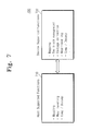
- the supported functions 700 include host supported functions 710 and device supported functions 720 .
- the host supported functions 710 include a mapping function, a wear-leveling function, and a compression/decompression function.
- the device supported functions 720 include a mapping function, a bad block management function, a garbage collection function, a wear-leveling function, a compression/decompression function, and possibly other functions.
- a query about the functionality of the host or the device would return an indication of the above supported functions, respectively.
- Both the host and the device may have one or more overlapping functions, so it remains to be determined which will actually implement each of the overlapping functions.
- FIG. 8 a set of negotiated partitioning parameters is indicated generally by the reference numeral 800 .
- “O” indicates that a local function is activated
- X indicates that a local function is not activated.
- the supported functions 800 include host supported functions 810 and device supported functions 820 .
- the host supported functions 810 include a mapping function that is activated on the host, a wear-leveling function that is activated on the host, and a compression/decompression function that is not activated on the host.
- the device supported functions 820 include a mapping function that is not activated on the device, a bad block management function that is activated on the device, a garbage collection function that is activated on the device, a wear-leveling function that is not activated on the device, a compression/decompression function that is activated on the device, and possibly other functions that may be activated on the device.
- a query about the active functions of the host or the device would return an indication of the above activated functions, respectively.
- Both the host and the device may have one or more overlapping functions, so a function activated on one of the host or device will generally not be activated on the other of the host or device, respectively.
- the communication method 900 includes associated host commands for the FTL functions activated on the host.
- the FTL functions activated on the host include a logical to physical mapping function 910 , a hot/cold data identification function 920 , and a data encryption function 930 .
- mapping function 910 causes the host to issue one of a plurality of mapping commands 912 , such as a flash read command, a flash write command, a flash copy command, or a flash erase command.
- mapping commands 912 such as a flash read command, a flash write command, a flash copy command, or a flash erase command.
- identification function 920 causes the host to issue one of a plurality of identification commands 922 , such as a command for writing to an SLC area, or a command for writing to an MLC area.
- encryption function 930 causes the host to issue one of a plurality of encryption commands 932 , such as a command for turning encryption on, or a command for turning encryption off.
Abstract
Description
Claims (51)
Priority Applications (3)
| Application Number | Priority Date | Filing Date | Title |
|---|---|---|---|
| DE200810008079 DE102008008079A1 (en) | 2007-02-01 | 2008-01-29 | Cooperative flash memory card system e.g. computer, has host providing memory management function for memory card device and issuing command to memory card device for enabling or disabling encryption or decryption |
| JP2008021198A JP5468207B2 (en) | 2007-02-01 | 2008-01-31 | Complementary memory management |
| TW097103746A TWI512459B (en) | 2007-02-01 | 2008-01-31 | Cooperative memory management and method thereof |
Applications Claiming Priority (3)
| Application Number | Priority Date | Filing Date | Title |
|---|---|---|---|
| KR1020070010573A KR100823171B1 (en) | 2007-02-01 | 2007-02-01 | Computer system having a partitioned flash translation layer and flash translation layer partition method thereof |
| KRP2007-0010573 | 2007-02-01 | ||
| KR10-2007-0010573 | 2007-02-01 |
Publications (2)
| Publication Number | Publication Date |
|---|---|
| US20080189485A1 US20080189485A1 (en) | 2008-08-07 |
| US8745309B2 true US8745309B2 (en) | 2014-06-03 |
Family
ID=39571848
Family Applications (1)
| Application Number | Title | Priority Date | Filing Date |
|---|---|---|---|
| US11/833,731 Active 2029-06-19 US8745309B2 (en) | 2007-02-01 | 2007-08-03 | Cooperative memory management |
Country Status (5)
| Country | Link |
|---|---|
| US (1) | US8745309B2 (en) |
| JP (1) | JP5468207B2 (en) |
| KR (1) | KR100823171B1 (en) |
| CN (1) | CN101236483A (en) |
| TW (1) | TWI512459B (en) |
Cited By (7)
| Publication number | Priority date | Publication date | Assignee | Title |
|---|---|---|---|---|
| US20130191609A1 (en) * | 2011-08-01 | 2013-07-25 | Atsushi Kunimatsu | Information processing device including host device and semiconductor memory device and semiconductor memory device |
| US9798657B2 (en) | 2014-10-15 | 2017-10-24 | Samsung Electronics Co., Ltd. | Data storage device including nonvolatile memory device and operating method thereof |
| US9928177B2 (en) * | 2013-08-21 | 2018-03-27 | Lite-On Electronics (Guangzhou) Limited | Managing method for cache memory of solid state drive |
| US10229051B2 (en) | 2015-12-30 | 2019-03-12 | Samsung Electronics Co., Ltd. | Storage device including nonvolatile memory device and controller, operating method of storage device, and method for accessing storage device |
| US10997066B2 (en) | 2018-02-20 | 2021-05-04 | Samsung Electronics Co., Ltd. | Storage devices that support cached physical address verification and methods of operating same |
| US11194489B2 (en) | 2020-04-27 | 2021-12-07 | Western Digital Technologies, Inc. | Zone-based device with control level selected by the host |
| US20230090549A1 (en) * | 2021-09-22 | 2023-03-23 | Toyota Motor Engineering & Manufacturing North America, Inc. | Data offloading rate determination using mean field games |
Families Citing this family (81)
| Publication number | Priority date | Publication date | Assignee | Title |
|---|---|---|---|---|
| US7917689B2 (en) * | 2007-12-28 | 2011-03-29 | Intel Corporation | Methods and apparatuses for nonvolatile memory wear leveling |
| US8307180B2 (en) | 2008-02-28 | 2012-11-06 | Nokia Corporation | Extended utilization area for a memory device |
| US7970978B2 (en) * | 2008-05-27 | 2011-06-28 | Initio Corporation | SSD with SATA and USB interfaces |
| US20090327535A1 (en) * | 2008-06-30 | 2009-12-31 | Liu Tz-Yi | Adjustable read latency for memory device in page-mode access |
| US20100017649A1 (en) * | 2008-07-19 | 2010-01-21 | Nanostar Corporation | Data storage system with wear-leveling algorithm |
| DE102008035095A1 (en) * | 2008-07-28 | 2010-02-11 | Vincotech (Germany) Gmbh | Method and device for detecting changes to data |
| US8108584B2 (en) * | 2008-10-15 | 2012-01-31 | Intel Corporation | Use of completer knowledge of memory region ordering requirements to modify transaction attributes |
| US8626984B2 (en) * | 2008-10-24 | 2014-01-07 | Cisco Technology, Inc. | Method and system for device independence in storage device wear algorithms |
| KR101543431B1 (en) * | 2008-11-20 | 2015-08-11 | 삼성전자주식회사 | Non-volatile memroy system and access method thereof |
| JP5221332B2 (en) * | 2008-12-27 | 2013-06-26 | 株式会社東芝 | Memory system |
| US8832354B2 (en) * | 2009-03-25 | 2014-09-09 | Apple Inc. | Use of host system resources by memory controller |
| US8874824B2 (en) | 2009-06-04 | 2014-10-28 | Memory Technologies, LLC | Apparatus and method to share host system RAM with mass storage memory RAM |
| KR101674015B1 (en) | 2009-06-23 | 2016-11-08 | 시게이트 테크놀로지 엘엘씨 | Data storage medium access method, data storage device and recording medium thereof |
| CN101706788B (en) * | 2009-11-25 | 2012-11-14 | 惠州Tcl移动通信有限公司 | Cross-area access method for embedded file system |
| CN102122267A (en) * | 2010-01-07 | 2011-07-13 | 上海华虹集成电路有限责任公司 | Multi-channel NANDflash controller capable of simultaneously carrying out data transmission and FTL (Flash Transition Layer) management |
| JP2011192239A (en) * | 2010-03-17 | 2011-09-29 | Sony Corp | Storage device and storage system |
| JP2011192240A (en) * | 2010-03-17 | 2011-09-29 | Sony Corp | Storage apparatus and storage system |
| WO2011148223A1 (en) * | 2010-05-27 | 2011-12-01 | Sandisk Il Ltd | Memory management storage to a host device |
| US8595415B2 (en) * | 2011-02-02 | 2013-11-26 | Micron Technology, Inc. | At least semi-autonomous modules in a memory system and methods |
| US8862902B2 (en) | 2011-04-29 | 2014-10-14 | Seagate Technology Llc | Cascaded data encryption dependent on attributes of physical memory |
| US8705291B2 (en) | 2011-05-27 | 2014-04-22 | Seagate Technology Llc | Sanitizing a non-volatile memory through charge accumulation |
| US20120317377A1 (en) * | 2011-06-09 | 2012-12-13 | Alexander Palay | Dual flash translation layer |
| US8645618B2 (en) * | 2011-07-14 | 2014-02-04 | Lsi Corporation | Flexible flash commands |
| US8806112B2 (en) | 2011-07-14 | 2014-08-12 | Lsi Corporation | Meta data handling within a flash media controller |
| JP5524144B2 (en) | 2011-08-08 | 2014-06-18 | 株式会社東芝 | Memory system having a key-value store system |
| US9323659B2 (en) * | 2011-08-12 | 2016-04-26 | Sandisk Enterprise Ip Llc | Cache management including solid state device virtualization |
| US8909855B2 (en) * | 2012-08-08 | 2014-12-09 | Avalanche Technology, Inc. | Storage system employing MRAM and physically addressed solid state disk |
| CN103946816B (en) * | 2011-09-30 | 2018-06-26 | 英特尔公司 | The nonvolatile RAM of replacement as conventional mass storage device(NVRAM) |
| CN102508787B (en) * | 2011-11-29 | 2014-09-03 | 清华大学 | System and method for memory allocation of composite memory |
| US9740439B2 (en) * | 2011-12-23 | 2017-08-22 | International Business Machines Corporation | Solid-state storage management |
| CN102541760B (en) * | 2012-01-04 | 2015-05-20 | 记忆科技(深圳)有限公司 | Computer system based on solid-state hard disk |
| US9213632B1 (en) | 2012-02-29 | 2015-12-15 | Marvell International Ltd. | Systems and methods for data storage devices to use external resources |
| TWI584120B (en) * | 2012-03-23 | 2017-05-21 | Lsi公司 | Method and system for dynamically adaptive caching |
| US9311226B2 (en) | 2012-04-20 | 2016-04-12 | Memory Technologies Llc | Managing operational state data of a memory module using host memory in association with state change |
| KR101419004B1 (en) * | 2012-05-03 | 2014-07-11 | 주식회사 디에이아이오 | Non-volatile memory system |
| US20140047159A1 (en) * | 2012-08-10 | 2014-02-13 | Sandisk Technologies Inc. | Enterprise server with flash storage modules |
| CN104583977B (en) * | 2012-08-23 | 2017-07-14 | 苹果公司 | The compression of the memory block of main frame auxiliary |
| KR101420754B1 (en) * | 2012-11-22 | 2014-07-17 | 주식회사 이에프텍 | Non-volatile memory system and method of managing a mapping table for the same |
| US9652376B2 (en) | 2013-01-28 | 2017-05-16 | Radian Memory Systems, Inc. | Cooperative flash memory control |
| US10642505B1 (en) | 2013-01-28 | 2020-05-05 | Radian Memory Systems, Inc. | Techniques for data migration based on per-data metrics and memory degradation |
| US11249652B1 (en) | 2013-01-28 | 2022-02-15 | Radian Memory Systems, Inc. | Maintenance of nonvolatile memory on host selected namespaces by a common memory controller |
| US9229854B1 (en) | 2013-01-28 | 2016-01-05 | Radian Memory Systems, LLC | Multi-array operation support and related devices, systems and software |
| US10445229B1 (en) | 2013-01-28 | 2019-10-15 | Radian Memory Systems, Inc. | Memory controller with at least one address segment defined for which data is striped across flash memory dies, with a common address offset being used to obtain physical addresses for the data in each of the dies |
| US9612973B2 (en) | 2013-11-09 | 2017-04-04 | Microsoft Technology Licensing, Llc | Using shared virtual memory resources for performing memory-mapping |
| KR101549569B1 (en) | 2014-02-14 | 2015-09-03 | 고려대학교 산학협력단 | Method for performing garbage collection and flash memory apparatus using the method |
| KR102147916B1 (en) | 2014-04-14 | 2020-08-26 | 삼성전자주식회사 | Nonvolatile memory system and operating mehtod thereof |
| CN105224474B (en) * | 2014-06-03 | 2019-05-31 | 深圳市腾讯计算机系统有限公司 | The realization system of solid state hard disk flash translation layer (FTL) and the realization device of flash translation layer (FTL) |
| KR20160022453A (en) | 2014-08-19 | 2016-03-02 | 삼성전자주식회사 | Mobile electronic device including embedded memory |
| US9542118B1 (en) | 2014-09-09 | 2017-01-10 | Radian Memory Systems, Inc. | Expositive flash memory control |
| US10552085B1 (en) | 2014-09-09 | 2020-02-04 | Radian Memory Systems, Inc. | Techniques for directed data migration |
| TWI567554B (en) | 2014-11-06 | 2017-01-21 | 慧榮科技股份有限公司 | Methods for caching and reading data to be written into a storage unit and apparatuses using the same |
| JP6378111B2 (en) * | 2014-12-29 | 2018-08-22 | 東芝メモリ株式会社 | Information processing apparatus and program |
| CN106201327B (en) * | 2015-01-22 | 2019-01-04 | 光宝科技股份有限公司 | System and its corresponding control methods with solid state storage device |
| US9880748B2 (en) * | 2015-02-13 | 2018-01-30 | Qualcomm Incorporated | Bifurcated memory management for memory elements |
| CN105005536B (en) * | 2015-07-01 | 2019-08-06 | 忆正科技(武汉)有限公司 | Solid storage device, the working method of host and solid storage device, host |
| US10055236B2 (en) | 2015-07-02 | 2018-08-21 | Sandisk Technologies Llc | Runtime data storage and/or retrieval |
| US10552058B1 (en) | 2015-07-17 | 2020-02-04 | Radian Memory Systems, Inc. | Techniques for delegating data processing to a cooperative memory controller |
| US10466908B2 (en) * | 2015-08-25 | 2019-11-05 | Toshiba Memory Corporation | Memory system that buffers data before writing to nonvolatile memory |
| US10459846B2 (en) * | 2015-09-10 | 2019-10-29 | Toshiba Memory Corporation | Memory system which uses a host memory |
| CN105353989B (en) * | 2015-11-19 | 2018-12-28 | 华为技术有限公司 | Storing data access method and relevant controller, equipment, host and system |
| US10033810B2 (en) | 2015-12-03 | 2018-07-24 | International Business Machines Corporation | Recovery point objective via dynamic usage of bind segments in a global mirror environment |
| CN107092560B (en) * | 2016-02-17 | 2020-06-16 | 建兴储存科技(广州)有限公司 | Solid-state storage device and flash translation layer mapping table rebuilding method applied to same |
| CN105867850B (en) * | 2016-03-29 | 2019-05-31 | 北京联想核芯科技有限公司 | A kind of information method of adjustment and electronic equipment |
| KR20170128012A (en) * | 2016-05-13 | 2017-11-22 | 주식회사 맴레이 | Flash-based storage and computing device |
| US10037152B2 (en) | 2016-12-19 | 2018-07-31 | Alibaba Group Holding Limited | Method and system of high-throughput high-capacity storage appliance with flash translation layer escalation and global optimization on raw NAND flash |
| US10971241B2 (en) | 2017-01-30 | 2021-04-06 | Toshiba Memory Corporation | Performance based method and system for patrolling read disturb errors in a memory unit |
| KR20190052366A (en) * | 2017-11-08 | 2019-05-16 | 에스케이하이닉스 주식회사 | Controller and operation method thereof |
| CN108287663A (en) * | 2017-12-21 | 2018-07-17 | 北京京存技术有限公司 | A kind of date storage method and device based on EMMC |
| US11436023B2 (en) | 2018-05-31 | 2022-09-06 | Pure Storage, Inc. | Mechanism for updating host file system and flash translation layer based on underlying NAND technology |
| US11263124B2 (en) | 2018-08-03 | 2022-03-01 | Micron Technology, Inc. | Host-resident translation layer validity check |
| CN111326195A (en) * | 2018-12-14 | 2020-06-23 | 北京兆易创新科技股份有限公司 | Memory device |
| US11226907B2 (en) | 2018-12-19 | 2022-01-18 | Micron Technology, Inc. | Host-resident translation layer validity check techniques |
| US11226894B2 (en) * | 2018-12-21 | 2022-01-18 | Micron Technology, Inc. | Host-based flash memory maintenance techniques |
| KR20200139913A (en) * | 2019-06-05 | 2020-12-15 | 에스케이하이닉스 주식회사 | Memory system, memory controller and meta infomation storage device |
| JP7252821B2 (en) * | 2019-04-17 | 2023-04-05 | キヤノン株式会社 | Recording device, recording method, program, and memory card |
| US11294825B2 (en) | 2019-04-17 | 2022-04-05 | SK Hynix Inc. | Memory system for utilizing a memory included in an external device |
| KR20200122086A (en) | 2019-04-17 | 2020-10-27 | 에스케이하이닉스 주식회사 | Apparatus and method for transmitting map segment in memory system |
| KR20210001546A (en) | 2019-06-28 | 2021-01-06 | 에스케이하이닉스 주식회사 | Apparatus and method for transmitting internal data of memory system in sleep mode |
| US11036594B1 (en) | 2019-07-25 | 2021-06-15 | Jetstream Software Inc. | Disaster recovery systems and methods with low recovery point objectives |
| US11175984B1 (en) | 2019-12-09 | 2021-11-16 | Radian Memory Systems, Inc. | Erasure coding techniques for flash memory |
| CN111415697B (en) * | 2020-03-20 | 2022-08-16 | 杭州华澜微电子股份有限公司 | Method, device and system for verifying flash translation layer algorithm |
Citations (42)
| Publication number | Priority date | Publication date | Assignee | Title |
|---|---|---|---|---|
| US4984190A (en) * | 1986-09-01 | 1991-01-08 | Nec Corporation | Serial data transfer system |
| JPH05173989A (en) | 1991-12-24 | 1993-07-13 | Kawasaki Steel Corp | Computer and multiprocessor computation device |
| US5319751A (en) * | 1991-12-27 | 1994-06-07 | Intel Corporation | Device driver configuration in a computer system |
| JPH0887441A (en) | 1994-09-19 | 1996-04-02 | Fujitsu Ltd | Flash memory access system |
| KR970071280A (en) | 1996-04-26 | 1997-11-07 | 포만 제프리 엘 | How to Allocate System Resources in a Hierarchical Bus Structure |
| US5687346A (en) * | 1994-09-30 | 1997-11-11 | Mitsubishi Denki Kabushiki Kaisha | PC card and PC card system with dual port ram and switchable rewritable ROM |
| JPH1063519A (en) | 1996-07-01 | 1998-03-06 | Sun Microsyst Inc | Method and system for reserving resource |
| US6081447A (en) | 1991-09-13 | 2000-06-27 | Western Digital Corporation | Wear leveling techniques for flash EEPROM systems |
| US6151709A (en) * | 1998-02-13 | 2000-11-21 | Novell, Inc. | Processes and apparatuses for uploading instructions to a computer |
| US6260102B1 (en) * | 1996-12-26 | 2001-07-10 | Intel Corporation | Interface for flash EEPROM memory arrays |
| JP2003022427A (en) | 2001-07-09 | 2003-01-24 | Hitachi Ltd | Storage device with uploading function |
| US20030221092A1 (en) * | 2002-05-23 | 2003-11-27 | Ballard Curtis C. | Method and system of switching between two or more images of firmware on a host device |
| US6701402B1 (en) * | 2001-03-30 | 2004-03-02 | Hewlett-Packard Development Company, L.P. | Selectively operating a host's device controller in a first mode or a second mode |
| KR20040082921A (en) | 2003-03-19 | 2004-09-30 | 삼성전자주식회사 | flash file system |
| US20050057973A1 (en) * | 2003-09-16 | 2005-03-17 | Micron Technology, Inc. | Runtime flash device detection and configuration for flash data management software |
| KR20050027233A (en) | 2005-02-03 | 2005-03-18 | 주식회사 퍼스터 | The method of nand flash memory access for the device under the file system |
| US20050073884A1 (en) | 2003-10-03 | 2005-04-07 | Gonzalez Carlos J. | Flash memory data correction and scrub techniques |
| US20050080986A1 (en) * | 2003-10-08 | 2005-04-14 | Samsung Electronics Co., Ltd. | Priority-based flash memory control apparatus for XIP in serial flash memory,memory management method using the same, and flash memory chip thereof |
| US20050144360A1 (en) | 2003-12-30 | 2005-06-30 | Bennett Alan D. | Non-volatile memory and method with block management system |
| WO2005066970A2 (en) | 2003-12-30 | 2005-07-21 | Sandisk Corporation | Robust data duplication and improved update method in a multibit non-volatile memory |
| KR20050078916A (en) | 2004-02-03 | 2005-08-08 | 삼성전자주식회사 | Data managing device and method for flash memory |
| US6938116B2 (en) | 2001-06-04 | 2005-08-30 | Samsung Electronics Co., Ltd. | Flash memory management method |
| US20050270993A1 (en) * | 2004-06-07 | 2005-12-08 | Krishnan Rajamani | Efficient partitioning of MAC (media access control) functions |
| US6990662B2 (en) * | 2001-10-31 | 2006-01-24 | Hewlett-Packard Development Company, L.P. | Method and system for offloading execution and resources for resource-constrained networked devices |
| US20060026334A1 (en) * | 2004-07-30 | 2006-02-02 | Adluri Mohan R | Operating system arrangement for flexible computer system design |
| US20060064538A1 (en) | 2004-09-22 | 2006-03-23 | Kabushiki Kaisha Toshiba | Memory controller, memory device and control method for the memory controller |
| US7039754B2 (en) * | 2002-04-15 | 2006-05-02 | Sony Corporation | Detachably mounted removable data storage device |
| US20060094477A1 (en) * | 2004-11-04 | 2006-05-04 | Motorola, Inc. | Power saving system and method |
| US20060130004A1 (en) | 2004-12-15 | 2006-06-15 | Microsoft Corporation | Portable applications |
| KR20060080972A (en) | 2005-01-06 | 2006-07-12 | 삼성전자주식회사 | Apparatus and method for storing data in nonvolatile cache memory considering update ratio |
| US20060157549A1 (en) * | 2005-01-14 | 2006-07-20 | Stein Israel M | Smart cards for automated sample analysis devices |
| KR20060090087A (en) | 2005-02-07 | 2006-08-10 | 삼성전자주식회사 | Adaptive flash memory control device with multiple mapping schemes and flash memory system havintg the same |
| KR20060090080A (en) | 2005-02-07 | 2006-08-10 | 삼성전자주식회사 | Run level address mapping table and forming method for the same |
| US20060184724A1 (en) * | 2005-02-11 | 2006-08-17 | M-Systems Flash Disk Pioneers, Ltd. | NAND flash memory system architecture |
| US20060184723A1 (en) * | 2005-02-16 | 2006-08-17 | Sinclair Alan W | Direct file data programming and deletion in flash memories |
| US20060209444A1 (en) * | 2005-03-17 | 2006-09-21 | Dong-Hyun Song | Hard disk drive with reduced power consumption, related data processing apparatus, and I/O method |
| WO2006123919A1 (en) | 2005-05-20 | 2006-11-23 | Mpio Co., Ltd. | Usb-sd memory device having dma channels and method of storing data in usb-sd memory device |
| JP2006338481A (en) | 2005-06-03 | 2006-12-14 | Tdk Corp | Memory controller, flash memory system, and method for controlling flash memory |
| KR20070008403A (en) | 2005-07-13 | 2007-01-17 | 삼성전자주식회사 | Data storing apparatus comprising complex memory and method of operating the same |
| US20070180186A1 (en) * | 2006-01-27 | 2007-08-02 | Cornwell Michael J | Non-volatile memory management |
| JP2008011512A (en) | 2006-06-01 | 2008-01-17 | Canon Inc | Data processing apparatus, data storage device and data processing methods therefor |
| US7966039B2 (en) * | 2007-02-02 | 2011-06-21 | Microsoft Corporation | Bidirectional dynamic offloading of tasks between a host and a mobile device |
Family Cites Families (4)
| Publication number | Priority date | Publication date | Assignee | Title |
|---|---|---|---|---|
| US6014724A (en) * | 1995-10-27 | 2000-01-11 | Scm Microsystems (U.S.) Inc. | Flash translation layer block indication map revision system and method |
| US5928347A (en) * | 1997-11-18 | 1999-07-27 | Shuttle Technology Group Ltd. | Universal memory card interface apparatus |
| KR100568115B1 (en) * | 2004-06-30 | 2006-04-05 | 삼성전자주식회사 | Incremental merge method and memory system using the same |
| JP4192129B2 (en) * | 2004-09-13 | 2008-12-03 | 株式会社東芝 | Memory management device |
-
2007
- 2007-02-01 KR KR1020070010573A patent/KR100823171B1/en active IP Right Grant
- 2007-08-03 US US11/833,731 patent/US8745309B2/en active Active
-
2008
- 2008-01-31 CN CNA200810008933XA patent/CN101236483A/en active Pending
- 2008-01-31 JP JP2008021198A patent/JP5468207B2/en active Active
- 2008-01-31 TW TW097103746A patent/TWI512459B/en active
Patent Citations (47)
| Publication number | Priority date | Publication date | Assignee | Title |
|---|---|---|---|---|
| US4984190A (en) * | 1986-09-01 | 1991-01-08 | Nec Corporation | Serial data transfer system |
| US6081447A (en) | 1991-09-13 | 2000-06-27 | Western Digital Corporation | Wear leveling techniques for flash EEPROM systems |
| JPH05173989A (en) | 1991-12-24 | 1993-07-13 | Kawasaki Steel Corp | Computer and multiprocessor computation device |
| US5319751A (en) * | 1991-12-27 | 1994-06-07 | Intel Corporation | Device driver configuration in a computer system |
| JPH0887441A (en) | 1994-09-19 | 1996-04-02 | Fujitsu Ltd | Flash memory access system |
| US5687346A (en) * | 1994-09-30 | 1997-11-11 | Mitsubishi Denki Kabushiki Kaisha | PC card and PC card system with dual port ram and switchable rewritable ROM |
| KR970071280A (en) | 1996-04-26 | 1997-11-07 | 포만 제프리 엘 | How to Allocate System Resources in a Hierarchical Bus Structure |
| JPH1063519A (en) | 1996-07-01 | 1998-03-06 | Sun Microsyst Inc | Method and system for reserving resource |
| US6260102B1 (en) * | 1996-12-26 | 2001-07-10 | Intel Corporation | Interface for flash EEPROM memory arrays |
| US6151709A (en) * | 1998-02-13 | 2000-11-21 | Novell, Inc. | Processes and apparatuses for uploading instructions to a computer |
| US6701402B1 (en) * | 2001-03-30 | 2004-03-02 | Hewlett-Packard Development Company, L.P. | Selectively operating a host's device controller in a first mode or a second mode |
| US6938116B2 (en) | 2001-06-04 | 2005-08-30 | Samsung Electronics Co., Ltd. | Flash memory management method |
| JP2003022427A (en) | 2001-07-09 | 2003-01-24 | Hitachi Ltd | Storage device with uploading function |
| US6990662B2 (en) * | 2001-10-31 | 2006-01-24 | Hewlett-Packard Development Company, L.P. | Method and system for offloading execution and resources for resource-constrained networked devices |
| US7039754B2 (en) * | 2002-04-15 | 2006-05-02 | Sony Corporation | Detachably mounted removable data storage device |
| US20030221092A1 (en) * | 2002-05-23 | 2003-11-27 | Ballard Curtis C. | Method and system of switching between two or more images of firmware on a host device |
| KR20040082921A (en) | 2003-03-19 | 2004-09-30 | 삼성전자주식회사 | flash file system |
| US20050057973A1 (en) * | 2003-09-16 | 2005-03-17 | Micron Technology, Inc. | Runtime flash device detection and configuration for flash data management software |
| US20050073884A1 (en) | 2003-10-03 | 2005-04-07 | Gonzalez Carlos J. | Flash memory data correction and scrub techniques |
| WO2005036401A2 (en) | 2003-10-03 | 2005-04-21 | Sandisk Corporation | Flash memory data correction and scrub techniques |
| US20050080986A1 (en) * | 2003-10-08 | 2005-04-14 | Samsung Electronics Co., Ltd. | Priority-based flash memory control apparatus for XIP in serial flash memory,memory management method using the same, and flash memory chip thereof |
| US20050144360A1 (en) | 2003-12-30 | 2005-06-30 | Bennett Alan D. | Non-volatile memory and method with block management system |
| WO2005066970A2 (en) | 2003-12-30 | 2005-07-21 | Sandisk Corporation | Robust data duplication and improved update method in a multibit non-volatile memory |
| KR20050078916A (en) | 2004-02-03 | 2005-08-08 | 삼성전자주식회사 | Data managing device and method for flash memory |
| US20050270993A1 (en) * | 2004-06-07 | 2005-12-08 | Krishnan Rajamani | Efficient partitioning of MAC (media access control) functions |
| US20060026334A1 (en) * | 2004-07-30 | 2006-02-02 | Adluri Mohan R | Operating system arrangement for flexible computer system design |
| US20060064538A1 (en) | 2004-09-22 | 2006-03-23 | Kabushiki Kaisha Toshiba | Memory controller, memory device and control method for the memory controller |
| JP2006092169A (en) | 2004-09-22 | 2006-04-06 | Toshiba Corp | Memory controller, memory device and control method for memory controller |
| US20060094477A1 (en) * | 2004-11-04 | 2006-05-04 | Motorola, Inc. | Power saving system and method |
| US20060130004A1 (en) | 2004-12-15 | 2006-06-15 | Microsoft Corporation | Portable applications |
| JP2006172449A (en) | 2004-12-15 | 2006-06-29 | Microsoft Corp | Portable applications |
| KR20060080972A (en) | 2005-01-06 | 2006-07-12 | 삼성전자주식회사 | Apparatus and method for storing data in nonvolatile cache memory considering update ratio |
| US20060157549A1 (en) * | 2005-01-14 | 2006-07-20 | Stein Israel M | Smart cards for automated sample analysis devices |
| KR20050027233A (en) | 2005-02-03 | 2005-03-18 | 주식회사 퍼스터 | The method of nand flash memory access for the device under the file system |
| KR20060090087A (en) | 2005-02-07 | 2006-08-10 | 삼성전자주식회사 | Adaptive flash memory control device with multiple mapping schemes and flash memory system havintg the same |
| KR20060090080A (en) | 2005-02-07 | 2006-08-10 | 삼성전자주식회사 | Run level address mapping table and forming method for the same |
| US20060184724A1 (en) * | 2005-02-11 | 2006-08-17 | M-Systems Flash Disk Pioneers, Ltd. | NAND flash memory system architecture |
| US20060184723A1 (en) * | 2005-02-16 | 2006-08-17 | Sinclair Alan W | Direct file data programming and deletion in flash memories |
| US20060209444A1 (en) * | 2005-03-17 | 2006-09-21 | Dong-Hyun Song | Hard disk drive with reduced power consumption, related data processing apparatus, and I/O method |
| WO2006123919A1 (en) | 2005-05-20 | 2006-11-23 | Mpio Co., Ltd. | Usb-sd memory device having dma channels and method of storing data in usb-sd memory device |
| US20080235410A1 (en) | 2005-05-20 | 2008-09-25 | Koh Kwang-Kyu | Usb-Sd Memory Device Having Dma Channels and Method of Storing Data in Usb-Sd Memory Device |
| JP2006338481A (en) | 2005-06-03 | 2006-12-14 | Tdk Corp | Memory controller, flash memory system, and method for controlling flash memory |
| KR20070008403A (en) | 2005-07-13 | 2007-01-17 | 삼성전자주식회사 | Data storing apparatus comprising complex memory and method of operating the same |
| US20070180186A1 (en) * | 2006-01-27 | 2007-08-02 | Cornwell Michael J | Non-volatile memory management |
| JP2008011512A (en) | 2006-06-01 | 2008-01-17 | Canon Inc | Data processing apparatus, data storage device and data processing methods therefor |
| US20100023781A1 (en) | 2006-06-01 | 2010-01-28 | Yasuhiro Nakamoto | Data processing apparatus, data storage device, and data processing method therefor |
| US7966039B2 (en) * | 2007-02-02 | 2011-06-21 | Microsoft Corporation | Bidirectional dynamic offloading of tasks between a host and a mobile device |
Non-Patent Citations (6)
| Title |
|---|
| English Abstract for Publication No. 2008-11512. |
| English Abstract for Publication No. JP2003-022427. |
| English Abstract for Publication No. JP2006-092169. |
| English Abstract for Publication No. JP2006172449. |
| English Abstract for Publication No. JP2006-338481. |
| English Abstract U.S. Patent No. 5,778,197 for Publication No. 97-71280. |
Cited By (18)
| Publication number | Priority date | Publication date | Assignee | Title |
|---|---|---|---|---|
| US10331356B2 (en) | 2011-08-01 | 2019-06-25 | Toshiba Memory Corporation | Data writing processing into memory of a semiconductor memory device by using a memory of a host device |
| US11537291B2 (en) | 2011-08-01 | 2022-12-27 | Kioxia Corporation | Data reading and writing processing from and to a semiconductor memory and a memory of a host device by using first and second interface circuits |
| US20130191609A1 (en) * | 2011-08-01 | 2013-07-25 | Atsushi Kunimatsu | Information processing device including host device and semiconductor memory device and semiconductor memory device |
| US10949092B2 (en) | 2011-08-01 | 2021-03-16 | Toshiba Memory Corporation | Memory system with block rearrangement to secure a free block based on read valid first and second data |
| US9870155B2 (en) | 2011-08-01 | 2018-01-16 | Toshiba Memory Corporation | Information processing device including host device and semiconductor memory device having a block rearrangement to secure free blocks |
| US9268706B2 (en) * | 2011-08-01 | 2016-02-23 | Kabushiki Kaisha Toshiba | Information processing device including host device and semiconductor memory device having plurality of address conversion information |
| US9542117B2 (en) | 2011-08-01 | 2017-01-10 | Kabushiki Kaisha Toshiba | Information processing device including host device and semiconductor memory device having a plurality of address conversion information |
| US11868618B2 (en) | 2011-08-01 | 2024-01-09 | Kioxia Corporation | Data reading and writing processing from and to a semiconductor memory and a memory of a host device by using first and second interface circuits |
| US9928177B2 (en) * | 2013-08-21 | 2018-03-27 | Lite-On Electronics (Guangzhou) Limited | Managing method for cache memory of solid state drive |
| US10133665B2 (en) | 2014-10-15 | 2018-11-20 | Samsung Electronics Co., Ltd. | Data storage device including nonvolatile memory device and operating method thereof |
| US9798657B2 (en) | 2014-10-15 | 2017-10-24 | Samsung Electronics Co., Ltd. | Data storage device including nonvolatile memory device and operating method thereof |
| US10671524B2 (en) | 2014-10-15 | 2020-06-02 | Samsung Electronics Co,. Ltd. | Data storage device including nonvolatile memory device and operating method thereof |
| US10229051B2 (en) | 2015-12-30 | 2019-03-12 | Samsung Electronics Co., Ltd. | Storage device including nonvolatile memory device and controller, operating method of storage device, and method for accessing storage device |
| US10997066B2 (en) | 2018-02-20 | 2021-05-04 | Samsung Electronics Co., Ltd. | Storage devices that support cached physical address verification and methods of operating same |
| US11775423B2 (en) | 2018-02-20 | 2023-10-03 | Samsung Electronics Co., Ltd. | Storage devices that support cached physical address verification and methods of operating same |
| US11194489B2 (en) | 2020-04-27 | 2021-12-07 | Western Digital Technologies, Inc. | Zone-based device with control level selected by the host |
| US20230090549A1 (en) * | 2021-09-22 | 2023-03-23 | Toyota Motor Engineering & Manufacturing North America, Inc. | Data offloading rate determination using mean field games |
| US11659028B2 (en) * | 2021-09-22 | 2023-05-23 | Toyota Motor Engineering & Manufacturing North America, Inc. | Data offloading rate determination using mean field games |
Also Published As
| Publication number | Publication date |
|---|---|
| TWI512459B (en) | 2015-12-11 |
| TW200839511A (en) | 2008-10-01 |
| CN101236483A (en) | 2008-08-06 |
| US20080189485A1 (en) | 2008-08-07 |
| JP2008192153A (en) | 2008-08-21 |
| KR100823171B1 (en) | 2008-04-18 |
| JP5468207B2 (en) | 2014-04-09 |
Similar Documents
| Publication | Publication Date | Title |
|---|---|---|
| US8745309B2 (en) | Cooperative memory management | |
| US8935459B2 (en) | Heuristics for programming data in a non-volatile memory | |
| KR101395778B1 (en) | Memory card and memory system including the same and operating method thereof | |
| US9304911B2 (en) | Semiconductor storage device and buffer operation method thereof | |
| JP5636034B2 (en) | Mediation of mount times for data usage | |
| US20140359382A1 (en) | Memory controller and operating method providing replacement block for bad block | |
| US11237742B2 (en) | Apparatus and method for controlling data stored in memory system | |
| US11755315B2 (en) | Boot ROM update method and boot-up method of embedded system | |
| US11249911B2 (en) | Storage device, memory system, and operating method for managing host-resident L2P map cache | |
| KR20120037786A (en) | Storage device, lock mode management method thereof and memory system having the same | |
| US20200320012A1 (en) | Memory system and method for operating the same | |
| CN108108261B (en) | Data storage device and operation method thereof | |
| US20190079830A1 (en) | Data storage device and operating method thereof | |
| KR20200113992A (en) | Apparatus and method for reducing cell disturb in open block of the memory system during receovery procedure | |
| KR20160074025A (en) | Operating method for data storage device | |
| US9734057B2 (en) | Semiconductor storage device and buffer operation method thereof | |
| US11281574B2 (en) | Apparatus and method for processing different types of data in memory system | |
| CN110806983B (en) | Memory system and operating method thereof | |
| CN112306906A (en) | Storage device, storage system including the same, and method of operating the same | |
| US20200250104A1 (en) | Apparatus and method for transmitting map information in a memory system | |
| CN112445424A (en) | Apparatus and method for improving input/output throughput of memory system | |
| EP3779704B1 (en) | Storage device, memory system comprising the same, and operating method thereof | |
| US11520896B2 (en) | Storage device | |
| EP4287028A1 (en) | Storage device providing high purge performance and memory block management method thereof | |
| KR20150072485A (en) | Data storage device and operating method thereof |
Legal Events
| Date | Code | Title | Description |
|---|---|---|---|
| AS | Assignment |
Owner name: SAMSUNG ELECTRONICS CO., LTD., KOREA, REPUBLIC OF Free format text: ASSIGNMENT OF ASSIGNORS INTEREST;ASSIGNORS:JUNG, MYOUNG-SOO;PARK, CHAN-IK;OH, SANG-JIN;REEL/FRAME:019977/0001 Effective date: 20071015 |
|
| STCF | Information on status: patent grant |
Free format text: PATENTED CASE |
|
| MAFP | Maintenance fee payment |
Free format text: PAYMENT OF MAINTENANCE FEE, 4TH YEAR, LARGE ENTITY (ORIGINAL EVENT CODE: M1551) Year of fee payment: 4 |
|
| MAFP | Maintenance fee payment |
Free format text: PAYMENT OF MAINTENANCE FEE, 8TH YEAR, LARGE ENTITY (ORIGINAL EVENT CODE: M1552); ENTITY STATUS OF PATENT OWNER: LARGE ENTITY Year of fee payment: 8 |