US8756777B2 - Method of manufacturing a ladder filter - Google Patents
Method of manufacturing a ladder filter Download PDFInfo
- Publication number
- US8756777B2 US8756777B2 US12/647,794 US64779409A US8756777B2 US 8756777 B2 US8756777 B2 US 8756777B2 US 64779409 A US64779409 A US 64779409A US 8756777 B2 US8756777 B2 US 8756777B2
- Authority
- US
- United States
- Prior art keywords
- film
- resonator
- piezoelectric
- lower electrode
- area
- Prior art date
- Legal status (The legal status is an assumption and is not a legal conclusion. Google has not performed a legal analysis and makes no representation as to the accuracy of the status listed.)
- Active, expires
Links
- 238000004519 manufacturing process Methods 0.000 title claims abstract description 5
- 239000000758 substrate Substances 0.000 claims abstract description 26
- 238000005530 etching Methods 0.000 claims abstract description 25
- 239000011796 hollow space material Substances 0.000 claims description 24
- 238000000034 method Methods 0.000 claims description 21
- 239000011651 chromium Substances 0.000 claims description 11
- 239000010936 titanium Substances 0.000 claims description 10
- XLOMVQKBTHCTTD-UHFFFAOYSA-N Zinc monoxide Chemical compound [Zn]=O XLOMVQKBTHCTTD-UHFFFAOYSA-N 0.000 claims description 9
- PMHQVHHXPFUNSP-UHFFFAOYSA-M copper(1+);methylsulfanylmethane;bromide Chemical compound Br[Cu].CSC PMHQVHHXPFUNSP-UHFFFAOYSA-M 0.000 claims description 7
- 238000001039 wet etching Methods 0.000 claims description 6
- NBIIXXVUZAFLBC-UHFFFAOYSA-N Phosphoric acid Chemical compound OP(O)(O)=O NBIIXXVUZAFLBC-UHFFFAOYSA-N 0.000 claims description 4
- 239000011787 zinc oxide Substances 0.000 claims description 4
- KJTLSVCANCCWHF-UHFFFAOYSA-N Ruthenium Chemical compound [Ru] KJTLSVCANCCWHF-UHFFFAOYSA-N 0.000 claims description 3
- 229910052719 titanium Inorganic materials 0.000 claims description 3
- RTAQQCXQSZGOHL-UHFFFAOYSA-N Titanium Chemical compound [Ti] RTAQQCXQSZGOHL-UHFFFAOYSA-N 0.000 claims description 2
- 229910000147 aluminium phosphate Inorganic materials 0.000 claims description 2
- 239000013078 crystal Substances 0.000 claims description 2
- 238000009413 insulation Methods 0.000 claims description 2
- 229910052707 ruthenium Inorganic materials 0.000 claims description 2
- VYZAMTAEIAYCRO-UHFFFAOYSA-N Chromium Chemical compound [Cr] VYZAMTAEIAYCRO-UHFFFAOYSA-N 0.000 claims 1
- 229910052804 chromium Inorganic materials 0.000 claims 1
- 239000004020 conductor Substances 0.000 abstract description 2
- 239000010408 film Substances 0.000 description 174
- 230000000052 comparative effect Effects 0.000 description 13
- 239000000463 material Substances 0.000 description 12
- 238000004544 sputter deposition Methods 0.000 description 8
- VYPSYNLAJGMNEJ-UHFFFAOYSA-N Silicium dioxide Chemical compound O=[Si]=O VYPSYNLAJGMNEJ-UHFFFAOYSA-N 0.000 description 7
- 239000010409 thin film Substances 0.000 description 7
- XUIMIQQOPSSXEZ-UHFFFAOYSA-N Silicon Chemical compound [Si] XUIMIQQOPSSXEZ-UHFFFAOYSA-N 0.000 description 6
- 230000000694 effects Effects 0.000 description 6
- 229910052710 silicon Inorganic materials 0.000 description 6
- 239000010703 silicon Substances 0.000 description 6
- 229910052814 silicon oxide Inorganic materials 0.000 description 6
- 238000010586 diagram Methods 0.000 description 5
- 238000001459 lithography Methods 0.000 description 5
- 239000000853 adhesive Substances 0.000 description 3
- 230000001070 adhesive effect Effects 0.000 description 3
- 238000005259 measurement Methods 0.000 description 3
- BASFCYQUMIYNBI-UHFFFAOYSA-N platinum Chemical compound [Pt] BASFCYQUMIYNBI-UHFFFAOYSA-N 0.000 description 3
- PIGFYZPCRLYGLF-UHFFFAOYSA-N Aluminum nitride Chemical compound [Al]#N PIGFYZPCRLYGLF-UHFFFAOYSA-N 0.000 description 2
- 230000008901 benefit Effects 0.000 description 2
- 239000010949 copper Substances 0.000 description 2
- 239000011521 glass Substances 0.000 description 2
- 239000000395 magnesium oxide Substances 0.000 description 2
- CPLXHLVBOLITMK-UHFFFAOYSA-N magnesium oxide Inorganic materials [Mg]=O CPLXHLVBOLITMK-UHFFFAOYSA-N 0.000 description 2
- AXZKOIWUVFPNLO-UHFFFAOYSA-N magnesium;oxygen(2-) Chemical compound [O-2].[Mg+2] AXZKOIWUVFPNLO-UHFFFAOYSA-N 0.000 description 2
- 238000001020 plasma etching Methods 0.000 description 2
- 230000008569 process Effects 0.000 description 2
- 230000004044 response Effects 0.000 description 2
- 239000010948 rhodium Substances 0.000 description 2
- 238000010897 surface acoustic wave method Methods 0.000 description 2
- RYGMFSIKBFXOCR-UHFFFAOYSA-N Copper Chemical compound [Cu] RYGMFSIKBFXOCR-UHFFFAOYSA-N 0.000 description 1
- 229910001218 Gallium arsenide Inorganic materials 0.000 description 1
- ZOKXTWBITQBERF-UHFFFAOYSA-N Molybdenum Chemical compound [Mo] ZOKXTWBITQBERF-UHFFFAOYSA-N 0.000 description 1
- 229910003781 PbTiO3 Inorganic materials 0.000 description 1
- ATJFFYVFTNAWJD-UHFFFAOYSA-N Tin Chemical group [Sn] ATJFFYVFTNAWJD-UHFFFAOYSA-N 0.000 description 1
- 229910052782 aluminium Inorganic materials 0.000 description 1
- XAGFODPZIPBFFR-UHFFFAOYSA-N aluminium Chemical compound [Al] XAGFODPZIPBFFR-UHFFFAOYSA-N 0.000 description 1
- 230000005540 biological transmission Effects 0.000 description 1
- 230000015556 catabolic process Effects 0.000 description 1
- 230000001413 cellular effect Effects 0.000 description 1
- 229910052802 copper Inorganic materials 0.000 description 1
- 238000006731 degradation reaction Methods 0.000 description 1
- NKZSPGSOXYXWQA-UHFFFAOYSA-N dioxido(oxo)titanium;lead(2+) Chemical compound [Pb+2].[O-][Ti]([O-])=O NKZSPGSOXYXWQA-UHFFFAOYSA-N 0.000 description 1
- 238000006073 displacement reaction Methods 0.000 description 1
- 238000001312 dry etching Methods 0.000 description 1
- 230000008020 evaporation Effects 0.000 description 1
- 238000001704 evaporation Methods 0.000 description 1
- 229910052732 germanium Inorganic materials 0.000 description 1
- 230000010354 integration Effects 0.000 description 1
- 229910052741 iridium Inorganic materials 0.000 description 1
- GKOZUEZYRPOHIO-UHFFFAOYSA-N iridium atom Chemical compound [Ir] GKOZUEZYRPOHIO-UHFFFAOYSA-N 0.000 description 1
- HFGPZNIAWCZYJU-UHFFFAOYSA-N lead zirconate titanate Chemical compound [O-2].[O-2].[O-2].[O-2].[O-2].[Ti+4].[Zr+4].[Pb+2] HFGPZNIAWCZYJU-UHFFFAOYSA-N 0.000 description 1
- 229910052751 metal Inorganic materials 0.000 description 1
- 239000002184 metal Substances 0.000 description 1
- 229910044991 metal oxide Inorganic materials 0.000 description 1
- 150000004706 metal oxides Chemical class 0.000 description 1
- 229910052750 molybdenum Inorganic materials 0.000 description 1
- 239000011733 molybdenum Substances 0.000 description 1
- 150000004767 nitrides Chemical class 0.000 description 1
- 229920002120 photoresistant polymer Polymers 0.000 description 1
- 229910052697 platinum Inorganic materials 0.000 description 1
- 239000010453 quartz Substances 0.000 description 1
- 238000012827 research and development Methods 0.000 description 1
- 229910052703 rhodium Inorganic materials 0.000 description 1
- MHOVAHRLVXNVSD-UHFFFAOYSA-N rhodium atom Chemical compound [Rh] MHOVAHRLVXNVSD-UHFFFAOYSA-N 0.000 description 1
- 230000007480 spreading Effects 0.000 description 1
- 229910052715 tantalum Inorganic materials 0.000 description 1
- GUVRBAGPIYLISA-UHFFFAOYSA-N tantalum atom Chemical compound [Ta] GUVRBAGPIYLISA-UHFFFAOYSA-N 0.000 description 1
- WFKWXMTUELFFGS-UHFFFAOYSA-N tungsten Chemical compound [W] WFKWXMTUELFFGS-UHFFFAOYSA-N 0.000 description 1
- 229910052721 tungsten Inorganic materials 0.000 description 1
- 239000010937 tungsten Substances 0.000 description 1
Images


Classifications
-
- H—ELECTRICITY
- H03—ELECTRONIC CIRCUITRY
- H03H—IMPEDANCE NETWORKS, e.g. RESONANT CIRCUITS; RESONATORS
- H03H3/00—Apparatus or processes specially adapted for the manufacture of impedance networks, resonating circuits, resonators
- H03H3/007—Apparatus or processes specially adapted for the manufacture of impedance networks, resonating circuits, resonators for the manufacture of electromechanical resonators or networks
- H03H3/02—Apparatus or processes specially adapted for the manufacture of impedance networks, resonating circuits, resonators for the manufacture of electromechanical resonators or networks for the manufacture of piezoelectric or electrostrictive resonators or networks
- H03H3/04—Apparatus or processes specially adapted for the manufacture of impedance networks, resonating circuits, resonators for the manufacture of electromechanical resonators or networks for the manufacture of piezoelectric or electrostrictive resonators or networks for obtaining desired frequency or temperature coefficient
-
- H—ELECTRICITY
- H03—ELECTRONIC CIRCUITRY
- H03H—IMPEDANCE NETWORKS, e.g. RESONANT CIRCUITS; RESONATORS
- H03H9/00—Networks comprising electromechanical or electro-acoustic devices; Electromechanical resonators
- H03H9/15—Constructional features of resonators consisting of piezoelectric or electrostrictive material
- H03H9/205—Constructional features of resonators consisting of piezoelectric or electrostrictive material having multiple resonators
-
- H—ELECTRICITY
- H03—ELECTRONIC CIRCUITRY
- H03H—IMPEDANCE NETWORKS, e.g. RESONANT CIRCUITS; RESONATORS
- H03H9/00—Networks comprising electromechanical or electro-acoustic devices; Electromechanical resonators
- H03H9/46—Filters
- H03H9/54—Filters comprising resonators of piezo-electric or electrostrictive material
-
- H—ELECTRICITY
- H03—ELECTRONIC CIRCUITRY
- H03H—IMPEDANCE NETWORKS, e.g. RESONANT CIRCUITS; RESONATORS
- H03H9/00—Networks comprising electromechanical or electro-acoustic devices; Electromechanical resonators
- H03H9/02—Details
- H03H9/02007—Details of bulk acoustic wave devices
- H03H9/02086—Means for compensation or elimination of undesirable effects
- H03H9/0211—Means for compensation or elimination of undesirable effects of reflections
-
- H—ELECTRICITY
- H03—ELECTRONIC CIRCUITRY
- H03H—IMPEDANCE NETWORKS, e.g. RESONANT CIRCUITS; RESONATORS
- H03H9/00—Networks comprising electromechanical or electro-acoustic devices; Electromechanical resonators
- H03H9/02—Details
- H03H9/02007—Details of bulk acoustic wave devices
- H03H9/02086—Means for compensation or elimination of undesirable effects
- H03H9/02118—Means for compensation or elimination of undesirable effects of lateral leakage between adjacent resonators
-
- H—ELECTRICITY
- H03—ELECTRONIC CIRCUITRY
- H03H—IMPEDANCE NETWORKS, e.g. RESONANT CIRCUITS; RESONATORS
- H03H9/00—Networks comprising electromechanical or electro-acoustic devices; Electromechanical resonators
- H03H9/02—Details
- H03H9/02007—Details of bulk acoustic wave devices
- H03H9/02086—Means for compensation or elimination of undesirable effects
- H03H9/02133—Means for compensation or elimination of undesirable effects of stress
-
- H—ELECTRICITY
- H03—ELECTRONIC CIRCUITRY
- H03H—IMPEDANCE NETWORKS, e.g. RESONANT CIRCUITS; RESONATORS
- H03H9/00—Networks comprising electromechanical or electro-acoustic devices; Electromechanical resonators
- H03H9/02—Details
- H03H9/02007—Details of bulk acoustic wave devices
- H03H9/02086—Means for compensation or elimination of undesirable effects
- H03H9/02149—Means for compensation or elimination of undesirable effects of ageing changes of characteristics, e.g. electro-acousto-migration
-
- H—ELECTRICITY
- H03—ELECTRONIC CIRCUITRY
- H03H—IMPEDANCE NETWORKS, e.g. RESONANT CIRCUITS; RESONATORS
- H03H9/00—Networks comprising electromechanical or electro-acoustic devices; Electromechanical resonators
- H03H9/02—Details
- H03H9/125—Driving means, e.g. electrodes, coils
- H03H9/13—Driving means, e.g. electrodes, coils for networks consisting of piezoelectric or electrostrictive materials
- H03H9/131—Driving means, e.g. electrodes, coils for networks consisting of piezoelectric or electrostrictive materials consisting of a multilayered structure
-
- H—ELECTRICITY
- H03—ELECTRONIC CIRCUITRY
- H03H—IMPEDANCE NETWORKS, e.g. RESONANT CIRCUITS; RESONATORS
- H03H9/00—Networks comprising electromechanical or electro-acoustic devices; Electromechanical resonators
- H03H9/02—Details
- H03H9/125—Driving means, e.g. electrodes, coils
- H03H9/13—Driving means, e.g. electrodes, coils for networks consisting of piezoelectric or electrostrictive materials
- H03H9/132—Driving means, e.g. electrodes, coils for networks consisting of piezoelectric or electrostrictive materials characterized by a particular shape
-
- H—ELECTRICITY
- H03—ELECTRONIC CIRCUITRY
- H03H—IMPEDANCE NETWORKS, e.g. RESONANT CIRCUITS; RESONATORS
- H03H9/00—Networks comprising electromechanical or electro-acoustic devices; Electromechanical resonators
- H03H9/15—Constructional features of resonators consisting of piezoelectric or electrostrictive material
- H03H9/17—Constructional features of resonators consisting of piezoelectric or electrostrictive material having a single resonator
- H03H9/171—Constructional features of resonators consisting of piezoelectric or electrostrictive material having a single resonator implemented with thin-film techniques, i.e. of the film bulk acoustic resonator [FBAR] type
- H03H9/172—Means for mounting on a substrate, i.e. means constituting the material interface confining the waves to a volume
- H03H9/173—Air-gaps
-
- H—ELECTRICITY
- H03—ELECTRONIC CIRCUITRY
- H03H—IMPEDANCE NETWORKS, e.g. RESONANT CIRCUITS; RESONATORS
- H03H9/00—Networks comprising electromechanical or electro-acoustic devices; Electromechanical resonators
- H03H9/15—Constructional features of resonators consisting of piezoelectric or electrostrictive material
- H03H9/17—Constructional features of resonators consisting of piezoelectric or electrostrictive material having a single resonator
- H03H9/171—Constructional features of resonators consisting of piezoelectric or electrostrictive material having a single resonator implemented with thin-film techniques, i.e. of the film bulk acoustic resonator [FBAR] type
- H03H9/172—Means for mounting on a substrate, i.e. means constituting the material interface confining the waves to a volume
- H03H9/174—Membranes
-
- H—ELECTRICITY
- H03—ELECTRONIC CIRCUITRY
- H03H—IMPEDANCE NETWORKS, e.g. RESONANT CIRCUITS; RESONATORS
- H03H9/00—Networks comprising electromechanical or electro-acoustic devices; Electromechanical resonators
- H03H9/46—Filters
- H03H9/54—Filters comprising resonators of piezo-electric or electrostrictive material
- H03H9/56—Monolithic crystal filters
- H03H9/566—Electric coupling means therefor
- H03H9/568—Electric coupling means therefor consisting of a ladder configuration
-
- H—ELECTRICITY
- H03—ELECTRONIC CIRCUITRY
- H03H—IMPEDANCE NETWORKS, e.g. RESONANT CIRCUITS; RESONATORS
- H03H9/00—Networks comprising electromechanical or electro-acoustic devices; Electromechanical resonators
- H03H9/46—Filters
- H03H9/54—Filters comprising resonators of piezo-electric or electrostrictive material
- H03H9/58—Multiple crystal filters
- H03H9/582—Multiple crystal filters implemented with thin-film techniques
- H03H9/586—Means for mounting to a substrate, i.e. means constituting the material interface confining the waves to a volume
- H03H9/587—Air-gaps
-
- H—ELECTRICITY
- H03—ELECTRONIC CIRCUITRY
- H03H—IMPEDANCE NETWORKS, e.g. RESONANT CIRCUITS; RESONATORS
- H03H9/00—Networks comprising electromechanical or electro-acoustic devices; Electromechanical resonators
- H03H9/46—Filters
- H03H9/54—Filters comprising resonators of piezo-electric or electrostrictive material
- H03H9/58—Multiple crystal filters
- H03H9/582—Multiple crystal filters implemented with thin-film techniques
- H03H9/586—Means for mounting to a substrate, i.e. means constituting the material interface confining the waves to a volume
- H03H9/588—Membranes
-
- H—ELECTRICITY
- H03—ELECTRONIC CIRCUITRY
- H03H—IMPEDANCE NETWORKS, e.g. RESONANT CIRCUITS; RESONATORS
- H03H9/00—Networks comprising electromechanical or electro-acoustic devices; Electromechanical resonators
- H03H9/46—Filters
- H03H9/54—Filters comprising resonators of piezo-electric or electrostrictive material
- H03H9/58—Multiple crystal filters
- H03H9/60—Electric coupling means therefor
- H03H9/605—Electric coupling means therefor consisting of a ladder configuration
-
- H—ELECTRICITY
- H03—ELECTRONIC CIRCUITRY
- H03H—IMPEDANCE NETWORKS, e.g. RESONANT CIRCUITS; RESONATORS
- H03H9/00—Networks comprising electromechanical or electro-acoustic devices; Electromechanical resonators
- H03H9/46—Filters
- H03H9/64—Filters using surface acoustic waves
- H03H9/6423—Means for obtaining a particular transfer characteristic
- H03H9/6433—Coupled resonator filters
- H03H9/6483—Ladder SAW filters
-
- H—ELECTRICITY
- H03—ELECTRONIC CIRCUITRY
- H03H—IMPEDANCE NETWORKS, e.g. RESONANT CIRCUITS; RESONATORS
- H03H3/00—Apparatus or processes specially adapted for the manufacture of impedance networks, resonating circuits, resonators
- H03H3/007—Apparatus or processes specially adapted for the manufacture of impedance networks, resonating circuits, resonators for the manufacture of electromechanical resonators or networks
- H03H3/02—Apparatus or processes specially adapted for the manufacture of impedance networks, resonating circuits, resonators for the manufacture of electromechanical resonators or networks for the manufacture of piezoelectric or electrostrictive resonators or networks
- H03H2003/021—Apparatus or processes specially adapted for the manufacture of impedance networks, resonating circuits, resonators for the manufacture of electromechanical resonators or networks for the manufacture of piezoelectric or electrostrictive resonators or networks the resonators or networks being of the air-gap type
-
- H—ELECTRICITY
- H03—ELECTRONIC CIRCUITRY
- H03H—IMPEDANCE NETWORKS, e.g. RESONANT CIRCUITS; RESONATORS
- H03H3/00—Apparatus or processes specially adapted for the manufacture of impedance networks, resonating circuits, resonators
- H03H3/007—Apparatus or processes specially adapted for the manufacture of impedance networks, resonating circuits, resonators for the manufacture of electromechanical resonators or networks
- H03H3/02—Apparatus or processes specially adapted for the manufacture of impedance networks, resonating circuits, resonators for the manufacture of electromechanical resonators or networks for the manufacture of piezoelectric or electrostrictive resonators or networks
- H03H2003/023—Apparatus or processes specially adapted for the manufacture of impedance networks, resonating circuits, resonators for the manufacture of electromechanical resonators or networks for the manufacture of piezoelectric or electrostrictive resonators or networks the resonators or networks being of the membrane type
-
- H—ELECTRICITY
- H03—ELECTRONIC CIRCUITRY
- H03H—IMPEDANCE NETWORKS, e.g. RESONANT CIRCUITS; RESONATORS
- H03H3/00—Apparatus or processes specially adapted for the manufacture of impedance networks, resonating circuits, resonators
- H03H3/007—Apparatus or processes specially adapted for the manufacture of impedance networks, resonating circuits, resonators for the manufacture of electromechanical resonators or networks
- H03H3/02—Apparatus or processes specially adapted for the manufacture of impedance networks, resonating circuits, resonators for the manufacture of electromechanical resonators or networks for the manufacture of piezoelectric or electrostrictive resonators or networks
- H03H3/04—Apparatus or processes specially adapted for the manufacture of impedance networks, resonating circuits, resonators for the manufacture of electromechanical resonators or networks for the manufacture of piezoelectric or electrostrictive resonators or networks for obtaining desired frequency or temperature coefficient
- H03H2003/0414—Resonance frequency
- H03H2003/0471—Resonance frequency of a plurality of resonators at different frequencies
-
- H—ELECTRICITY
- H03—ELECTRONIC CIRCUITRY
- H03H—IMPEDANCE NETWORKS, e.g. RESONANT CIRCUITS; RESONATORS
- H03H3/00—Apparatus or processes specially adapted for the manufacture of impedance networks, resonating circuits, resonators
-
- H—ELECTRICITY
- H03—ELECTRONIC CIRCUITRY
- H03H—IMPEDANCE NETWORKS, e.g. RESONANT CIRCUITS; RESONATORS
- H03H3/00—Apparatus or processes specially adapted for the manufacture of impedance networks, resonating circuits, resonators
- H03H3/007—Apparatus or processes specially adapted for the manufacture of impedance networks, resonating circuits, resonators for the manufacture of electromechanical resonators or networks
- H03H3/0072—Apparatus or processes specially adapted for the manufacture of impedance networks, resonating circuits, resonators for the manufacture of electromechanical resonators or networks of microelectro-mechanical resonators or networks
- H03H3/0073—Integration with other electronic structures
-
- H—ELECTRICITY
- H03—ELECTRONIC CIRCUITRY
- H03H—IMPEDANCE NETWORKS, e.g. RESONANT CIRCUITS; RESONATORS
- H03H9/00—Networks comprising electromechanical or electro-acoustic devices; Electromechanical resonators
- H03H9/15—Constructional features of resonators consisting of piezoelectric or electrostrictive material
- H03H9/17—Constructional features of resonators consisting of piezoelectric or electrostrictive material having a single resonator
- H03H9/178—Constructional features of resonators consisting of piezoelectric or electrostrictive material having a single resonator of a laminated structure of multiple piezoelectric layers with inner electrodes
-
- Y—GENERAL TAGGING OF NEW TECHNOLOGICAL DEVELOPMENTS; GENERAL TAGGING OF CROSS-SECTIONAL TECHNOLOGIES SPANNING OVER SEVERAL SECTIONS OF THE IPC; TECHNICAL SUBJECTS COVERED BY FORMER USPC CROSS-REFERENCE ART COLLECTIONS [XRACs] AND DIGESTS
- Y10—TECHNICAL SUBJECTS COVERED BY FORMER USPC
- Y10T—TECHNICAL SUBJECTS COVERED BY FORMER US CLASSIFICATION
- Y10T29/00—Metal working
- Y10T29/42—Piezoelectric device making
-
- Y—GENERAL TAGGING OF NEW TECHNOLOGICAL DEVELOPMENTS; GENERAL TAGGING OF CROSS-SECTIONAL TECHNOLOGIES SPANNING OVER SEVERAL SECTIONS OF THE IPC; TECHNICAL SUBJECTS COVERED BY FORMER USPC CROSS-REFERENCE ART COLLECTIONS [XRACs] AND DIGESTS
- Y10—TECHNICAL SUBJECTS COVERED BY FORMER USPC
- Y10T—TECHNICAL SUBJECTS COVERED BY FORMER US CLASSIFICATION
- Y10T29/00—Metal working
- Y10T29/49—Method of mechanical manufacture
- Y10T29/49002—Electrical device making
- Y10T29/49005—Acoustic transducer
-
- Y—GENERAL TAGGING OF NEW TECHNOLOGICAL DEVELOPMENTS; GENERAL TAGGING OF CROSS-SECTIONAL TECHNOLOGIES SPANNING OVER SEVERAL SECTIONS OF THE IPC; TECHNICAL SUBJECTS COVERED BY FORMER USPC CROSS-REFERENCE ART COLLECTIONS [XRACs] AND DIGESTS
- Y10—TECHNICAL SUBJECTS COVERED BY FORMER USPC
- Y10T—TECHNICAL SUBJECTS COVERED BY FORMER US CLASSIFICATION
- Y10T29/00—Metal working
- Y10T29/49—Method of mechanical manufacture
- Y10T29/49002—Electrical device making
- Y10T29/49117—Conductor or circuit manufacturing
- Y10T29/49124—On flat or curved insulated base, e.g., printed circuit, etc.
-
- Y—GENERAL TAGGING OF NEW TECHNOLOGICAL DEVELOPMENTS; GENERAL TAGGING OF CROSS-SECTIONAL TECHNOLOGIES SPANNING OVER SEVERAL SECTIONS OF THE IPC; TECHNICAL SUBJECTS COVERED BY FORMER USPC CROSS-REFERENCE ART COLLECTIONS [XRACs] AND DIGESTS
- Y10—TECHNICAL SUBJECTS COVERED BY FORMER USPC
- Y10T—TECHNICAL SUBJECTS COVERED BY FORMER US CLASSIFICATION
- Y10T29/00—Metal working
- Y10T29/49—Method of mechanical manufacture
- Y10T29/49002—Electrical device making
- Y10T29/49117—Conductor or circuit manufacturing
- Y10T29/49204—Contact or terminal manufacturing
- Y10T29/49208—Contact or terminal manufacturing by assembling plural parts
-
- Y—GENERAL TAGGING OF NEW TECHNOLOGICAL DEVELOPMENTS; GENERAL TAGGING OF CROSS-SECTIONAL TECHNOLOGIES SPANNING OVER SEVERAL SECTIONS OF THE IPC; TECHNICAL SUBJECTS COVERED BY FORMER USPC CROSS-REFERENCE ART COLLECTIONS [XRACs] AND DIGESTS
- Y10—TECHNICAL SUBJECTS COVERED BY FORMER USPC
- Y10T—TECHNICAL SUBJECTS COVERED BY FORMER US CLASSIFICATION
- Y10T29/00—Metal working
- Y10T29/49—Method of mechanical manufacture
- Y10T29/49002—Electrical device making
- Y10T29/49117—Conductor or circuit manufacturing
- Y10T29/49204—Contact or terminal manufacturing
- Y10T29/49224—Contact or terminal manufacturing with coating
Definitions
- the present invention relates to ladder type filters, and more particularly, to a ladder type filter using a piezoelectric thin-film resonator.
- the piezoelectric thin-film resonators may be categorized into an FBAR (Film Bulk Acoustic Resonator) type and an SMR (Solidly Mounted Resonator) type.
- the FBAR has a primary structure composed of an upper electrode, a piezoelectric film and a lower electrode, and a hollow space provided below the lower electrode and located within an overlapping region (resonance portion) in which the upper and lower electrodes overlap with each other across the piezoelectric film.
- the hollow space may be defined between the lower electrode and a silicon substrate by wet-etching a sacrificed layer on a main surface of the silicon substrate.
- the hollow space may also be formed by wet- or dry-etching the substrate from the backside thereof.
- the SMR employs an acoustic reflection film instead of the hollow space, in which a first film having a relatively high acoustic impedance and a second film having a relative low acoustic impedance are alternately laminated with a film thickness of ⁇ /4 where ⁇ is the wavelength of an acoustic wave of the resonator.
- the upper and lower electrodes may be made of aluminum (Al), copper (Cu), molybdenum (Mo), tungsten (W), tantalum (Ta), platinum (Pt), ruthenium (Ru), rhodium (Rh), iridium (Ir) or the like.
- the piezoelectric thin film may be made of aluminum nitride (AlN), zinc oxide (ZnO), lead zirconium titanate (PZT), lead titanate (PbTiO 3 ) or the like.
- the substrate may be made of glass other than silicon.
- a voltage of a high frequency is applied between the upper electrode and the lower electrode.
- An acoustic wave resulting from the inverse piezoelectric effect is excited within the piezoelectric film in the resonance portion.
- a distortion of the piezoelectric film caused by the acoustic wave is converted into an electric signal developing between the upper electrode and the lower electrode due to the piezoelectric effect.
- the acoustic wave is reflected by an interface between the air and the upper electrode and another interface between the air and the lower electrode.
- the resonant phenomenon of the vertical vibration is utilized to form a resonator having a desired frequency response and a filter using such a resonator.
- V denotes the propagation velocity of the acoustic wave that depends on the material used to form the piezoelectric film
- the resonance frequency F is equal to nV/(2H). This shows that the resonance frequency F can be controlled by the total thickness H of the film laminate.
- a ladder filter is a typical example of the piezoelectric thin-film resonator.
- the ladder filter is composed of series resonators arranged between an input terminal and an output terminal and parallel resonators, and functions as a bandpass filter.
- FIG. 1A shows an equivalent circuit of a series resonator S
- FIG. 1B shows an equivalent circuit of a parallel resonator P
- FIG. 1C shows transmission characteristics of the series resonator S and the parallel resonator P.
- the series resonator S has a maximum value at a resonance frequency frs and a minimum value at an anti-resonance frequency fas.
- the parallel resonator P has a minimum value at a resonance frequency frp and a maximum value at an anti-resonance frequency fap.
- FIG. 2A shows an equivalent circuit of a ladder filter composed of a single stage formed by one series resonator S and one parallel resonator P.
- FIG. 2B shows a bandpass characteristic of the ladder filter shown in FIG. 2A .
- the bandpass filter can be configured by setting the resonance frequency frs of the series resonator S and the anti-resonance frequency fap of the parallel resonator P approximately equal to each other.
- the anti-resonance frequency fas of the series resonator S corresponds to the frequency of an attenuation pole on the high-frequency side of the pass band
- the resonance frequency frp of the parallel resonator P corresponds to the frequency of an attenuation pole on the low-frequency side.
- the resonance frequencies of the series resonator S and the parallel resonator P are designed to have a slight difference (normally, a few %).
- a frequency adjustment step ( ⁇ f adjustment step) is needed to make the series resonator S and the parallel resonator P.
- the center frequency of the pass band can be adjusted by adjusting the resonance frequencies of both the series resonator S and the parallel resonator P (f 0 adjustment step).
- Japanese Patent Application Publication No. 2005-286945 discloses a technique in which a first adjustment film and a second adjustment film are stacked on an upper electrode as a frequency adjustment film, and the first adjustment films on the series resonator S and the parallel resonator P are made different from each other in thickness.
- the ⁇ f adjustment step is implemented by setting the first adjustment films on the series resonator S and the parallel resonator P different from each other in thickness
- the f 0 frequency adjustment is implemented by adjusting the thickness of the second adjustment film of each of the series resonator S and the parallel resonator P.
- the ⁇ f adjustment step and the f 0 adjustment step can be performed separately.
- Japanese Patent Application Publication No. 2006-128993 discloses that an edge of a piezoelectric film is located further in than an edge of a region in which the upper and lower electrodes overlap with each other. With this structure, it is possible to prevent the acoustic wave from leaking outwards from the resonance portion. This is called lateral leakage of acoustic wave.
- the structure may be formed by wet etching the piezoelectric film.
- the technique disclosed in Japanese Patent Application Publication No. 2005-286945 employs the ⁇ f adjustment step of causing the first adjustment films of the series resonator and the parallel resonator to have different thickness values.
- the first adjustment film of the series resonator is etched and thinned.
- the present invention has been made in view of the above circumstances and provides a ladder filter capable of reliably setting the difference between the resonance frequency of the series resonator and that of the parallel resonator.
- a ladder filter including: a series resonator having a first film laminate in which an upper electrode and a lower electrode face each other across a piezoelectric film, and a first film provided on the first film laminate; and a parallel resonator having a second film laminate having a structure similar to that of the first film laminate, a second film provided on the second film laminate, and another first film identical to the first film.
- FIG. 1A is an equivalent circuit diagram of a series resonator
- FIG. 1B is an equivalent circuit diagram of a parallel resonator
- FIG. 1C is a graph of frequency characteristics of the series resonator and the parallel resonator
- FIG. 2A is an equivalent circuit diagram of a ladder filter of a single stage
- FIG. 2B is a bandpass characteristic of the ladder filter
- FIG. 3 is an equivalent circuit diagram of a ladder filter in accordance with a first embodiment of the present invention.
- FIG. 4A is composed of a part (a) that shows a plan view of a series resonator employed in the first embodiment, and a part (b) that shows a cross-sectional view taken along a line A-A in part (a);
- FIG. 4B is a cross-sectional view of a parallel resonator taken along line A-A;
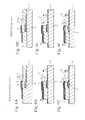
- FIGS. 5A through 5F are cross-sectional views of a method for manufacturing the series and parallel resonators
- FIGS. 6A through 6F are cross-sectional views of a subsequent process of the method.
- FIGS. 7A , 7 B and 7 C are plan view of a region 50 and its vicinity
- FIG. 8 is a cross-sectional view of a parallel resonator in accordance with a first comparative example
- FIG. 9A is a Smith chart of characteristics of resonators of the first comparative example.
- FIG. 9B is a Smith chart of characteristics of resonators of the first embodiment
- FIG. 10A is a graph of a bandpass characteristic of the first comparative example
- FIG. 10B is a graph of a bandpass characteristic of the first embodiment
- FIG. 11 is composed of a part (a) that shows a plan view of a parallel resonator in accordance with a second embodiment, and a part (b) that shows a cross-sectional view taken along a line A-A shown in part (a); and
- FIG. 12 is a plan view of a parallel resonator in accordance with a third embodiment.
- FIG. 3 is a circuit diagram of a ladder filter in accordance with a first embodiment of the present invention.
- Series resonators S 1 , S 2 and S 3 are connected in series between an input terminal Tin and an output terminal Tout.
- a parallel resonator P 1 is connected to a node between the series resonators S 1 and S 2 and ground.
- a parallel resonator P 2 is connected to a node between the series resonators S 2 and S 3 and ground.
- the series resonators S (S denotes any of S 1 through S 3 ) and the parallel resonators P (P denotes any of P 1 and P 2 ) have different structures, as will be described later.
- a part (a) of FIG. 4A shows a plan view of the series resonator S, and a part (b) shows a cross-sectional view taken along a line A-A shown in part (a).
- a lower electrode 12 is provided on a silicon substrate 10 so as to form a hollow space 30 that is formed between the silicon substrate 10 and the lower electrode 12 and is oriented upwards.
- the hollow space 30 is be defined by a raised portion of the lower electrode 12 having a dome shape.
- the hollow space 30 may be referred to as a dome-shaped hollow space.
- the dome-shaped portion of the lower electrode 12 may have a gradually increasing height towards the center of the hollow space 30 from its periphery.
- the lower electrode 12 may have Ru/Cr (ruthenium/chromium) structure.
- a piezoelectric film 14 that may be made of, for example, aluminum nitride (AlN) and has the main axis in the (002) direction, is provided on the lower electrode 12 .
- An upper electrode 16 is provided on the piezoelectric film 14 so that an overlapping region (resonance portion 52 ) can be defined in which the upper electrode 16 overlaps with the lower electrode 12 across the piezoelectric film 14 .
- the upper electrode 16 may be made, for example, Ru.
- the lower electrode 12 , the piezoelectric film 14 and the upper electrode 16 form a film laminate 18 .
- a first film 22 made of Cr is provided on the upper electrode 16 .
- a third film 24 which may be made of, for example, silicon oxide (SiO 2 ), is provided on the first film 22 , the substrate 10 and the piezoelectric film 14 .
- a guide path 32 for etching a sacrificed layer, which will be described later, is provided in the lower electrode 12 so as to run in a direction B-B.
- An end of the guide path 32 is not covered with the piezoelectric film 14 , and apertures 34 are formed in the lower electrode 12 and are connected to the ends of the guide path 32 .
- An opening 36 is provided in the piezoelectric film 14 for making an electric connection with the lower electrode 12 . In the opening 36 , at least a part of an outer curved edge 42 of the piezoelectric film 14 is further in, by a distance “d”, than an outer curved edge of a region 50 in which the upper electrode 16 overlaps with the lower electrode 12 across the piezoelectric film 14 .
- the parallel resonator P will now be described with reference to FIG. 4B , which shows a cross-sectional view taken along the line A-A of the parallel resonator P.
- the parallel resonator P differs from the above-mentioned series resonator S in that a second film 20 made of, for example, titanium (Ti), is provided between the upper electrode 16 and the first film 22 .
- the other structures of the parallel resonator P are the same as those of the series resonator S.
- the laminate that contributes the resonance frequency of the resonance portion 52 of the series resonator S is, from the top, SiO 2 /Cr/Ru/AlN/Ru/Cr.
- the laminate that contributes the resonance frequency of the resonance portion 52 of the parallel resonator P is, from the top, SiO 2 /Cr/Ti/Ru/AlN/Ru/Cr.
- the parallel resonator P is provided with the second film made of Ti, and can be designed to have a different resonance frequency from that of the series resonator S.
- a response of the bandpass filter a shown in FIG. 2B can be obtained.
- a sacrificed layer 38 made of MgO is deposited on the silicon substrate 10 by sputtering so as to have a thickness of approximately 40 nm.
- the sacrificed layer 38 is formed into a given shape by lithography and etching.
- the next step is to deposit a Cr film having a thickness of approximately 100 nm and a Ru film having a thickness of approximately 250 nm by sputtering. Then, the film laminate is shaped into the lower electrode 12 by the lithography and etching.
- AlN for the piezoelectric film 14 is deposited to a thickness of 1150 nm on the lower electrode 12 and the substrate 10 by sputtering. Then, a Ru film having a thickness of 250 nm for the upper electrode 16 is formed on the piezoelectric film 14 by sputtering.
- a Ti film having a thickness of 115 nm for the second film 20 is formed by sputtering so as to cover the upper electrode 16 . Then, using lithography and etching, the second film 20 is etched so that it remains on the sacrificed layer 38 of the parallel resonator P and does not remain thereon in the series resonator S. In this etching, the Ti film and the Ru film are etched with a selectivity, so that the second film 20 can be etched without losing the thickness of the upper electrode 16 .
- FIG. 7A shows a positional relationship between the upper electrode 16 , the second film 20 and a region (which will become the region 50 and will be referred to as region 50 for the convenience' sake) in the parallel resonator P.
- the second film 20 is formed so as to include the region 50 .
- a Cr film having a thickness of approximately 20 nm for the first film 22 is deposited on the upper electrode 16 and the second film 20 by sputtering.
- the first film 22 is formed into a given shape by lithography and etching.
- FIG. 7B shows a positional relationship between the upper electrode 16 , the second film 20 , the first film 22 and the region 50 in the parallel resonator P.
- the second film 20 is etched.
- the outer curved edges of the upper electrode 16 , the first film 22 and the second film 20 are aligned with each other on the right side of the region 50 .
- the second film 20 is greater than the region 50 on the left side of the region 50 .
- the outer curved edges of the upper electrode 16 and the first film 22 are aligned with each other.
- the piezoelectric film 14 is etched by lithography and etching. This etching may be wet etching using a phosphoric acid. The piezoelectric film 14 is over-etched, so that the outer curved edge of the piezoelectric film 14 can be further in than the region 50 .
- the third film 24 made of SiO 2 is formed on the first film 22 , the substrate 10 and the piezoelectric film 14 .
- FIG. 7C shows a positional relationship between the lower electrode 12 , the upper electrode 16 , the second film 20 , the first film 22 and the region 50 in the parallel resonator P.
- the outer curved edge of the piezoelectric film 14 is further in than the region 50 on the right side of the region 50 .
- the outer curved edge of the resonance portion 52 is further in than the outer edge of the region 50 on the right side of the region 50 .
- the outer curved edge of the resonance portion 52 coincides with the outer curved edge of the region 50 on the left side of the region 50 .
- etchant for etching the sacrificed layer 38 is applied to the guide path 32 (see FIG. 4A ) through the apertures 34 , and the sacrificed layer 38 is removed.
- the stress of the film laminate 18 composed of the lower electrode 12 , the piezoelectric film 14 and the upper electrode 16 is set so as to be compressive stress by adjusting the sputtering conditions for the respective films.
- the film laminate is raised so that the dome-shaped hollow space 30 oriented towards the film laminate 18 can be formed between the lower electrode 12 and the substrate 10 .
- the compressive stress may be set in the range of ⁇ 150 MPa to ⁇ 300 MPa.
- FIG. 8 is a cross-sectional view of a ladder filter in accordance with the first comparative example.
- a second film 20 a of the first comparative example is provided between the first film 22 and the third film 24 .
- the first comparative example may be fabricated by forming the second film 20 and the first film in the reverse sequence in FIGS. 5C and 5F . That is, in FIGS. 6B and 6E , when the piezoelectric film 14 is etched, the second film 20 is merely protected by photoresist.
- FIGS. 9A and 9B are Smith charts of the first comparative example and the first embodiment, respectively, in which the S 11 characteristics of three parallel resonators in a wafer are shown.
- the resonators used for measurement have an oval shape of the resonance portion 50 having a major axis of 247 ⁇ m and a minor axis of 176 ⁇ m.
- the distance “d” in FIG. 4B is selected so that lateral leakage of acoustic wave can be restrained.
- the three resonators of the first embodiment have almost the same the S 11 characteristics. In contrast, the three resonators of the first comparative example have different S 11 characteristics.
- FIGS. 10A and 10B show bandpass characteristics of the first comparative example and the first embodiment, respectively, in each of which the bandpass characteristics of formed in a wafer are shown.
- the regions 50 of the parallel resonators P of the ladder filters used for measurement have an oval shape that typically has a major axis of 180 ⁇ m and a minor axis of 151 ⁇ m.
- the parallel resonators P in each ladder filter have respective oval shapes having slightly different sizes.
- the regions 50 of the series resonators S of the ladder filters used for measurement have an oval shape that typically has a major axis of 233 ⁇ m and a minor axis of 195 ⁇ m.
- the series resonators S in each ladder filter have respective oval shapes having slightly different sizes.
- the distance “d” in FIGS. 4 A(b) and 4 B is selected so that lateral leakage of acoustic wave can be restrained.
- a great ripple takes place in the pass band, whereas the first embodiment does not have any considerable ripple.
- the first embodiment is capable of realizing the ladder filters having little difference in the bandpass characteristic and having suppressed ripples.
- the first film 22 is provided on the film laminate 18 .
- the second film 20 is provided on the film laminate 18 , and the first film 22 is provided on the second film 20 .
- the presence/absence of the second film 20 defines the difference ⁇ f between the resonance frequency of the series resonator S and that of the parallel resonator P.
- the first films 22 of the series resonator S and the parallel resonator P are made of an identical material.
- another film may be formed on the first film 22 of the series resonator S and that of the parallel resonator P with almost the same adhesiveness.
- films that contact resist (not shown) in the series resonator S and the parallel resonator P at the time of etching the piezoelectric film 14 are the first films 22 in the first embodiment.
- the first film 22 contacts resist (not shown) in the series resonator S
- the second film 20 a contacts resist (not shown) in the parallel resonator P at the time of etching the piezoelectric film 14 .
- Ti of the second film 20 a is likely to be etched in wet etching and is weaker in adhesive strength to the resist than Cr of the first film 22 .
- the second film 20 a is unwillingly etched.
- the degree of etching of the second film 20 a depends on the position on the wafer. This leads to deviations in the resonance characteristic and those in the bandpass characteristic.
- the second film 20 has a good etching selectivity to the upper electrode 16 .
- the first film 22 is made of a material having a strong adhesive strength to another film. This is taken into consideration in the first embodiment. That is, the first film 22 is provided on the film laminate 18 in the series resonators S, and the second film 20 is provided between the film laminate 18 and the first film 22 in the parallel resonators P. It is thus possible to prevent the thickness of the upper electrode 16 from being reduced to due to over etching at the time of forming the second film 20 and to prevent the difference ⁇ f between the series resonator S and the parallel resonator P from deviating from the target values. It is further possible to form films on the first films 22 in the series resonator S and the parallel resonator P with an increased and identical adhesive strength.
- the first film 22 may be made of a material having good adhesiveness to another material
- the second film 20 is made of a material having a good etching selectivity to the upper electrode 16
- the first film 22 and the second film 20 are made of an electrically conductive material in order to cause these films to function as the upper electrode 16 .
- the third films 24 are provided on the first films 22 in the series resonators S and the parallel resonators P.
- the third films 24 of the series resonators S and the parallel resonators P can be simultaneously etched, so that the resonance frequencies of the series resonators S and the parallel resonators P can be simultaneously adjusted. It is thus possible to adjust the center frequency f 0 of the pass band.
- the third film 24 is made of a material that makes it possible for the first film 22 , the second film 20 and the film laminate 18 to be etched during the f 0 adjustment.
- the third film 24 also functions as a protection film for the first film 22 , the second film 20 and the film laminate 18 .
- the third film 24 is an insulation film such as a metal oxide film or a metal nitride film.
- the region provided with the second film 20 includes the region 50 in which the upper electrode 16 faces the lower electrode 12 across the piezoelectric film 14 . If there is a part of the region 50 in which the second film 20 is not formed, the resonance characteristic will deviate from the designed characteristic.
- the first films 22 in the series resonators S and the first films 22 in the parallel resonators P have an identical thickness. It is thus possible to adjust the frequency difference ⁇ f by only the thickness of the second films 20 and to suppress the deviations of the characteristics.
- the hollow space has a dome shape that is oriented upwards, that is, towards the film laminate 18 . It is thus unnecessary to etch the substrate 10 . This improves the productivity and prevents degradation of the mechanical strength of the substrate 10 . Further, only a small region is needed to form the hollow space 30 , and the integration can be facilitated.
- the miniaturized hollow space 30 prevents the reliability of the film laminate 18 from being degraded due to mechanical vibrations. Further, the miniaturized hollow space 30 makes it possible to thin the sacrificed layer 38 and to secure good orientation of the piezoelectric film 14 .
- the film laminate 18 composed of the lower electrode 12 , the piezoelectric film 14 and the upper electrode 16 has compressive stress. It is thus possible to reliably form the dome-shaped hollow space 30 .
- the apertures 34 connected to the hollow space 30 are formed in the lower electrode 12 .
- the sacrificed layer 38 is etched through the apertures 34 , so that the dome-shaped hollow space 30 can be defined.
- the region 50 in which the upper electrode 16 faces the lower electrode 12 across the piezoelectric film 14 is included in a region formed by projecting the hollow space 30 onto the substrate 10 . This allows the film laminate 18 to vibrate.
- the piezoelectric film 14 may be made of aluminum nitride or zinc oxide having an orientation having the main axis in the (002) direction. It is thus possible to provide the piezoelectric thin-film resonators having good resonance characteristics.
- a second embodiment has a structure in which a hollow space 30 a is provided in the substrate 10 .
- a part (a) of FIG. 11 is a plan view of a resonator according to the second embodiment, and a part (b) thereof is a cross-sectional view taken along a line A-A.
- the hollow space 30 a is formed in the substrate 10 below the region 50 in which the upper electrode 16 faces the lower electrode 12 across the piezoelectric film 14 .
- the hollow space 30 a may be formed so as to have a substantially vertical wall by deep-RIE (reactive ion etching).
- FIG. 12 is a plan view of a series resonator S and a parallel resonator P in accordance with a third embodiment.
- the region 50 in which the upper electrode 16 faces the lower electrode 12 across the piezoelectric film 14 has a polygonal shape composed of anti-parallel sides.
- the other structures of the third embodiment are the same as those of the first embodiment.
- the region 50 may have an oval shape in the first embodiment, or a polygonal shape composed of anti-parallel sides in the second embodiment. There are no parallel sides in the region 50 . It is thus possible to prevent the acoustic wave reflected by the outer edge of the piezoelectric film 14 from being reflected and remaining in the resonance portion 52 as a standing wave in the lateral directions. It is thus possible to prevent ripples from taking place in the pass band.
- the first through third embodiments are ladder filters using FBARs.
- the present invention includes ladder filters using SMRs.
- the substrate 10 may be made of quartz crystal, glass or GaAs.
- the lower electrode 12 and the upper electrode 16 may be made of not only Ru but also another material as described in the Description of the Related Art.
- the sacrificed layer 38 may be made of a material that is easily removable by etchant.
- the sacrificed layer 38 may be made of ZnO, Ge or Ti.
- the films may be formed by evaporation other than sputtering.
- the first film 22 is not limited to the Cr film but may be made of another material as long as similar effects are obtained.
- the second film 20 is not limited to the Ti film but may be made of another material as long as similar effects are obtained.
- the third film 24 is not limited to SiO 2 but may be made of another material with similar effects are obtained.
Abstract
Description
Claims (14)
Priority Applications (1)
| Application Number | Priority Date | Filing Date | Title |
|---|---|---|---|
| US12/647,794 US8756777B2 (en) | 2006-10-17 | 2009-12-28 | Method of manufacturing a ladder filter |
Applications Claiming Priority (4)
| Application Number | Priority Date | Filing Date | Title |
|---|---|---|---|
| JP2006282290A JP4968900B2 (en) | 2006-10-17 | 2006-10-17 | Manufacturing method of ladder filter |
| JP2006-282290 | 2006-10-17 | ||
| US11/907,704 US20080129417A1 (en) | 2006-10-17 | 2007-10-16 | Ladder type filter |
| US12/647,794 US8756777B2 (en) | 2006-10-17 | 2009-12-28 | Method of manufacturing a ladder filter |
Related Parent Applications (1)
| Application Number | Title | Priority Date | Filing Date |
|---|---|---|---|
| US11/907,704 Division US20080129417A1 (en) | 2006-10-17 | 2007-10-16 | Ladder type filter |
Publications (2)
| Publication Number | Publication Date |
|---|---|
| US20100096358A1 US20100096358A1 (en) | 2010-04-22 |
| US8756777B2 true US8756777B2 (en) | 2014-06-24 |
Family
ID=38871740
Family Applications (2)
| Application Number | Title | Priority Date | Filing Date |
|---|---|---|---|
| US11/907,704 Abandoned US20080129417A1 (en) | 2006-10-17 | 2007-10-16 | Ladder type filter |
| US12/647,794 Active 2031-02-09 US8756777B2 (en) | 2006-10-17 | 2009-12-28 | Method of manufacturing a ladder filter |
Family Applications Before (1)
| Application Number | Title | Priority Date | Filing Date |
|---|---|---|---|
| US11/907,704 Abandoned US20080129417A1 (en) | 2006-10-17 | 2007-10-16 | Ladder type filter |
Country Status (5)
| Country | Link |
|---|---|
| US (2) | US20080129417A1 (en) |
| EP (1) | EP1914888B1 (en) |
| JP (1) | JP4968900B2 (en) |
| KR (1) | KR100906551B1 (en) |
| CN (1) | CN101166020A (en) |
Families Citing this family (30)
| Publication number | Priority date | Publication date | Assignee | Title |
|---|---|---|---|---|
| JP4252584B2 (en) * | 2006-04-28 | 2009-04-08 | 富士通メディアデバイス株式会社 | Piezoelectric thin film resonator and filter |
| JP5207902B2 (en) * | 2008-09-29 | 2013-06-12 | 京セラ株式会社 | Bulk acoustic wave resonators and electronic components |
| US8902023B2 (en) * | 2009-06-24 | 2014-12-02 | Avago Technologies General Ip (Singapore) Pte. Ltd. | Acoustic resonator structure having an electrode with a cantilevered portion |
| US10461719B2 (en) * | 2009-06-24 | 2019-10-29 | Avago Technologies International Sales Pte. Limited | Acoustic resonator structure having an electrode with a cantilevered portion |
| US9520856B2 (en) | 2009-06-24 | 2016-12-13 | Avago Technologies General Ip (Singapore) Pte. Ltd. | Acoustic resonator structure having an electrode with a cantilevered portion |
| US9673778B2 (en) | 2009-06-24 | 2017-06-06 | Avago Technologies General Ip (Singapore) Pte. Ltd. | Solid mount bulk acoustic wave resonator structure comprising a bridge |
| US8248185B2 (en) | 2009-06-24 | 2012-08-21 | Avago Technologies Wireless Ip (Singapore) Pte. Ltd. | Acoustic resonator structure comprising a bridge |
| JP5319491B2 (en) | 2009-10-22 | 2013-10-16 | 太陽誘電株式会社 | Piezoelectric thin film resonator |
| US9219464B2 (en) | 2009-11-25 | 2015-12-22 | Avago Technologies General Ip (Singapore) Pte. Ltd. | Bulk acoustic wave (BAW) resonator structure having an electrode with a cantilevered portion and a piezoelectric layer with multiple dopants |
| US9450561B2 (en) | 2009-11-25 | 2016-09-20 | Avago Technologies General Ip (Singapore) Pte. Ltd. | Bulk acoustic wave (BAW) resonator structure having an electrode with a cantilevered portion and a piezoelectric layer with varying amounts of dopant |
| US8384497B2 (en) * | 2009-12-18 | 2013-02-26 | Hao Zhang | Piezoelectric resonator structure having an interference structure |
| JP2011160232A (en) * | 2010-02-01 | 2011-08-18 | Ube Industries Ltd | Thin-film piezoelectric resonator, and thin-film piezoelectric filter using the same |
| WO2011099381A1 (en) * | 2010-02-09 | 2011-08-18 | 株式会社村田製作所 | Piezoelectric device, and piezoelectric device manufacturing method |
| JP5390431B2 (en) * | 2010-02-24 | 2014-01-15 | 太陽誘電株式会社 | Elastic wave device |
| US9148117B2 (en) | 2011-02-28 | 2015-09-29 | Avago Technologies General Ip (Singapore) Pte. Ltd. | Coupled resonator filter comprising a bridge and frame elements |
| US9136818B2 (en) | 2011-02-28 | 2015-09-15 | Avago Technologies General Ip (Singapore) Pte. Ltd. | Stacked acoustic resonator comprising a bridge |
| US9099983B2 (en) | 2011-02-28 | 2015-08-04 | Avago Technologies General Ip (Singapore) Pte. Ltd. | Bulk acoustic wave resonator device comprising a bridge in an acoustic reflector |
| US9203374B2 (en) | 2011-02-28 | 2015-12-01 | Avago Technologies General Ip (Singapore) Pte. Ltd. | Film bulk acoustic resonator comprising a bridge |
| US9425764B2 (en) | 2012-10-25 | 2016-08-23 | Avago Technologies General Ip (Singapore) Pte. Ltd. | Accoustic resonator having composite electrodes with integrated lateral features |
| US9444426B2 (en) | 2012-10-25 | 2016-09-13 | Avago Technologies General Ip (Singapore) Pte. Ltd. | Accoustic resonator having integrated lateral feature and temperature compensation feature |
| CN104702239B (en) * | 2011-06-23 | 2017-09-22 | 天工滤波方案日本有限公司 | Ladder-type acoustic wave filter and the antenna diplexer using the acoustic wave filter |
| JP5792554B2 (en) | 2011-08-09 | 2015-10-14 | 太陽誘電株式会社 | Elastic wave device |
| JP5815329B2 (en) * | 2011-08-22 | 2015-11-17 | 太陽誘電株式会社 | Elastic wave device |
| US9608592B2 (en) | 2014-01-21 | 2017-03-28 | Avago Technologies General Ip (Singapore) Pte. Ltd. | Film bulk acoustic wave resonator (FBAR) having stress-relief |
| JP6175743B2 (en) | 2012-06-06 | 2017-08-09 | セイコーエプソン株式会社 | Manufacturing method of vibration element |
| JP6185292B2 (en) * | 2013-06-10 | 2017-08-23 | 太陽誘電株式会社 | Elastic wave device |
| JP5681303B2 (en) * | 2014-01-07 | 2015-03-04 | 太陽誘電株式会社 | Elastic wave device |
| KR101942731B1 (en) * | 2017-04-10 | 2019-01-28 | 삼성전기 주식회사 | Filter and filter module |
| JP6925877B2 (en) * | 2017-06-07 | 2021-08-25 | 太陽誘電株式会社 | Elastic wave device |
| KR102149386B1 (en) * | 2019-04-16 | 2020-08-28 | 삼성전기주식회사 | Acoustic resonator and acoustic resonator filter |
Citations (21)
| Publication number | Priority date | Publication date | Assignee | Title |
|---|---|---|---|---|
| US5910756A (en) * | 1997-05-21 | 1999-06-08 | Nokia Mobile Phones Limited | Filters and duplexers utilizing thin film stacked crystal filter structures and thin film bulk acoustic wave resonators |
| US6407649B1 (en) | 2001-01-05 | 2002-06-18 | Nokia Corporation | Monolithic FBAR duplexer and method of making the same |
| US6518860B2 (en) | 2001-01-05 | 2003-02-11 | Nokia Mobile Phones Ltd | BAW filters having different center frequencies on a single substrate and a method for providing same |
| US6670866B2 (en) * | 2002-01-09 | 2003-12-30 | Nokia Corporation | Bulk acoustic wave resonator with two piezoelectric layers as balun in filters and duplexers |
| US6734763B2 (en) | 2001-10-26 | 2004-05-11 | Fujitsu Limited | Thin-film piezoelectric resonator, band-pass filter and method of making thin-film piezoelectric resonator |
| US20050046519A1 (en) | 2003-08-27 | 2005-03-03 | Tsuyoshi Yokoyama | Film bulk acoustic resonator and method of producing the same |
| US20050146242A1 (en) | 2003-12-18 | 2005-07-07 | Tdk Corporation | Electronic component and filter including the same |
| US20050152110A1 (en) | 2004-01-13 | 2005-07-14 | Winston Chen | Portable raid device |
| US6933809B2 (en) | 2003-04-07 | 2005-08-23 | Samsung Electro-Mechanics Co., Ltd. | Film bulk acoustic resonator (FBAR) device and method for producing the same |
| EP1583233A1 (en) | 2004-03-31 | 2005-10-05 | Fujitsu Media Devices Limited | Resonator, filter and fabrication of resonator |
| US6963257B2 (en) * | 2004-03-19 | 2005-11-08 | Nokia Corporation | Coupled BAW resonator based duplexers |
| US20050264137A1 (en) | 2004-05-31 | 2005-12-01 | Shinji Taniguchi | Piezoelectric thin-film resonator and filter and fabricating method |
| JP2006020277A (en) | 2004-06-03 | 2006-01-19 | Sony Corp | Thin film bulk acoustic resonator and method of manufacturing the same |
| US7019604B2 (en) | 2002-07-23 | 2006-03-28 | Murata Manufacturing Co., Ltd. | Piezoelectric filter, duplexer, composite piezoelectric resonator, communication device and method for adjusting frequency of piezoelectric filter |
| EP1653612A2 (en) | 2004-10-28 | 2006-05-03 | Fujitsu Media Devices Limited | Piezoelectric thin-film resonator and filter using the same |
| US20060152110A1 (en) | 2005-01-12 | 2006-07-13 | Fujitsu Media Devices Limited | Piezoelectric thin-film resonator and filter using the same |
| US20070096597A1 (en) | 2005-10-27 | 2007-05-03 | Fujitsu Media Devices Limited & Fujitsu Limited | Piezoelectric thin-film resonator and filter |
| US7221242B2 (en) | 2004-12-24 | 2007-05-22 | Hitachi Media Electronics Co., Ltd | Bulk acoustic wave resonator and manufacturing method thereof, filter using the same, semiconductor integrated circuit device using the same, and high frequency module using the same |
| US7554422B2 (en) * | 2004-09-10 | 2009-06-30 | Panasonic Corporation | Filter module using piezoelectric resonators, duplexer, communication device, and method for fabricating filter module |
| US7586391B2 (en) * | 2006-08-28 | 2009-09-08 | Stmicroelectronics Sa | Switchable filter with resonators |
| US7701117B2 (en) * | 2005-06-30 | 2010-04-20 | Panasonic Corporation | Acoustic resonator and filter |
Family Cites Families (1)
| Publication number | Priority date | Publication date | Assignee | Title |
|---|---|---|---|---|
| TW200610266A (en) * | 2004-06-03 | 2006-03-16 | Sony Corp | Thin film bulk acoustic resonator and method of manufacturing the same |
-
2006
- 2006-10-17 JP JP2006282290A patent/JP4968900B2/en active Active
-
2007
- 2007-10-16 KR KR1020070103934A patent/KR100906551B1/en active IP Right Grant
- 2007-10-16 US US11/907,704 patent/US20080129417A1/en not_active Abandoned
- 2007-10-16 EP EP07118583.9A patent/EP1914888B1/en not_active Expired - Fee Related
- 2007-10-17 CN CNA2007101819528A patent/CN101166020A/en active Pending
-
2009
- 2009-12-28 US US12/647,794 patent/US8756777B2/en active Active
Patent Citations (29)
| Publication number | Priority date | Publication date | Assignee | Title |
|---|---|---|---|---|
| US5910756A (en) * | 1997-05-21 | 1999-06-08 | Nokia Mobile Phones Limited | Filters and duplexers utilizing thin film stacked crystal filter structures and thin film bulk acoustic wave resonators |
| US6407649B1 (en) | 2001-01-05 | 2002-06-18 | Nokia Corporation | Monolithic FBAR duplexer and method of making the same |
| US20020089393A1 (en) | 2001-01-05 | 2002-07-11 | Pasi Tikka | Monolithic fbar duplexer and method of making the same |
| JP2002268644A (en) | 2001-01-05 | 2002-09-20 | Nokia Corp | Monolithic fbar duplexer and method for manufacturing the same |
| US6518860B2 (en) | 2001-01-05 | 2003-02-11 | Nokia Mobile Phones Ltd | BAW filters having different center frequencies on a single substrate and a method for providing same |
| US6734763B2 (en) | 2001-10-26 | 2004-05-11 | Fujitsu Limited | Thin-film piezoelectric resonator, band-pass filter and method of making thin-film piezoelectric resonator |
| US6670866B2 (en) * | 2002-01-09 | 2003-12-30 | Nokia Corporation | Bulk acoustic wave resonator with two piezoelectric layers as balun in filters and duplexers |
| US7019604B2 (en) | 2002-07-23 | 2006-03-28 | Murata Manufacturing Co., Ltd. | Piezoelectric filter, duplexer, composite piezoelectric resonator, communication device and method for adjusting frequency of piezoelectric filter |
| US6933809B2 (en) | 2003-04-07 | 2005-08-23 | Samsung Electro-Mechanics Co., Ltd. | Film bulk acoustic resonator (FBAR) device and method for producing the same |
| US20050046519A1 (en) | 2003-08-27 | 2005-03-03 | Tsuyoshi Yokoyama | Film bulk acoustic resonator and method of producing the same |
| US20050146242A1 (en) | 2003-12-18 | 2005-07-07 | Tdk Corporation | Electronic component and filter including the same |
| US20050152110A1 (en) | 2004-01-13 | 2005-07-14 | Winston Chen | Portable raid device |
| US6963257B2 (en) * | 2004-03-19 | 2005-11-08 | Nokia Corporation | Coupled BAW resonator based duplexers |
| US7498717B2 (en) * | 2004-03-31 | 2009-03-03 | Fujitsu Media Devices Limited | Resonator, filter and fabrication of resonator |
| US20050218754A1 (en) | 2004-03-31 | 2005-10-06 | Tsuyoshi Yokoyama | Resonator, filter and fabrication of resonator |
| EP1583233A1 (en) | 2004-03-31 | 2005-10-05 | Fujitsu Media Devices Limited | Resonator, filter and fabrication of resonator |
| JP2005286945A (en) | 2004-03-31 | 2005-10-13 | Fujitsu Media Device Kk | Resonator, filter and manufacture of resonator |
| US20050264137A1 (en) | 2004-05-31 | 2005-12-01 | Shinji Taniguchi | Piezoelectric thin-film resonator and filter and fabricating method |
| JP2006020277A (en) | 2004-06-03 | 2006-01-19 | Sony Corp | Thin film bulk acoustic resonator and method of manufacturing the same |
| US7554422B2 (en) * | 2004-09-10 | 2009-06-30 | Panasonic Corporation | Filter module using piezoelectric resonators, duplexer, communication device, and method for fabricating filter module |
| EP1653612A2 (en) | 2004-10-28 | 2006-05-03 | Fujitsu Media Devices Limited | Piezoelectric thin-film resonator and filter using the same |
| JP2006128993A (en) | 2004-10-28 | 2006-05-18 | Fujitsu Media Device Kk | Piezoelectric thin film resonator and filter using the same |
| US7221242B2 (en) | 2004-12-24 | 2007-05-22 | Hitachi Media Electronics Co., Ltd | Bulk acoustic wave resonator and manufacturing method thereof, filter using the same, semiconductor integrated circuit device using the same, and high frequency module using the same |
| KR20060082413A (en) | 2005-01-12 | 2006-07-18 | 후지쯔 가부시끼가이샤 | Piezoelectric thin-film resonator and filter using the same |
| EP1684424A1 (en) | 2005-01-12 | 2006-07-26 | Fujitsu Media Devices Limited | Piezoelectric thin-film resonator and filter using the same |
| US20060152110A1 (en) | 2005-01-12 | 2006-07-13 | Fujitsu Media Devices Limited | Piezoelectric thin-film resonator and filter using the same |
| US7701117B2 (en) * | 2005-06-30 | 2010-04-20 | Panasonic Corporation | Acoustic resonator and filter |
| US20070096597A1 (en) | 2005-10-27 | 2007-05-03 | Fujitsu Media Devices Limited & Fujitsu Limited | Piezoelectric thin-film resonator and filter |
| US7586391B2 (en) * | 2006-08-28 | 2009-09-08 | Stmicroelectronics Sa | Switchable filter with resonators |
Non-Patent Citations (4)
| Title |
|---|
| Japanese Office Action in a counterpart Japanese patent application No. 2006-282290, dated May 10, 2011, citing Foreign Patent document No. 1 listed above and JP2005-286945, which has been submitted in a previous IDS. |
| Lakin, K.M., "Thin Film Resonator Technology", 2003 IEEE International Frequency Control Symposium & PDA Exhibition jointly with the 17th European Frequency and Time Forum, May 4, 2003, pp. 765-778. |
| Park, Y.U. et al., "Comparison of Micromachined FAR Band pass Filters with Different Structural Geometry," 2003 IEEE MTT-S International Microwave Symposium Digest, Jun. 8-13, 2003, pp. 2005-2005, vol. 3. |
| Schmidhammer, E., et al., "Design Flow and Methodology on the Design of BAW Components," IEEE Microwave Symposium Digest, Jun. 12, 2005, pp. 233-236. |
Also Published As
| Publication number | Publication date |
|---|---|
| KR20080034790A (en) | 2008-04-22 |
| JP2008103798A (en) | 2008-05-01 |
| JP4968900B2 (en) | 2012-07-04 |
| CN101166020A (en) | 2008-04-23 |
| US20080129417A1 (en) | 2008-06-05 |
| EP1914888A1 (en) | 2008-04-23 |
| KR100906551B1 (en) | 2009-07-07 |
| US20100096358A1 (en) | 2010-04-22 |
| EP1914888B1 (en) | 2013-06-12 |
Similar Documents
| Publication | Publication Date | Title |
|---|---|---|
| US8756777B2 (en) | Method of manufacturing a ladder filter | |
| JP4223428B2 (en) | Filter and manufacturing method thereof | |
| US7737806B2 (en) | Piezoelectric thin-film resonator and filter | |
| KR100841166B1 (en) | Piezoelectric thin-film resonator and filter having the same | |
| US7128941B2 (en) | Method for fabricating film bulk acoustic resonator (FBAR) device | |
| KR100771345B1 (en) | Piezoelectric thin-film resonator and filter | |
| US7545077B2 (en) | Filter having multiple piezoelectric thin-film resonators | |
| JP4688070B2 (en) | Piezoelectric thin film resonator, piezoelectric thin film device, and manufacturing method thereof | |
| US8749320B2 (en) | Acoustic wave device and method for manufacturing the same | |
| KR20180107852A (en) | Acoustic resonator and manufacturing method thereof | |
| US8344590B2 (en) | Acoustic wave device with frequency control film | |
| KR20180131313A (en) | Acoustic resonator and method for fabricating the same | |
| JP5390431B2 (en) | Elastic wave device | |
| US10554196B2 (en) | Acoustic wave device | |
| CN117526892A (en) | Film bulk acoustic resonator, manufacturing method thereof and electronic equipment |
Legal Events
| Date | Code | Title | Description |
|---|---|---|---|
| AS | Assignment |
Owner name: FUJITSU MEDIA DEVICES LIMITED,JAPAN Free format text: ASSIGNMENT OF ASSIGNORS INTEREST;ASSIGNORS:TANIGUCHI, SHINJI;NISHIHARA, TOKIHIRO;YOKOYAMA, TSUYOSHI;AND OTHERS;SIGNING DATES FROM 20080124 TO 20080130;REEL/FRAME:023707/0120 Owner name: FUJITSU LIMITED,JAPAN Free format text: ASSIGNMENT OF ASSIGNORS INTEREST;ASSIGNORS:TANIGUCHI, SHINJI;NISHIHARA, TOKIHIRO;YOKOYAMA, TSUYOSHI;AND OTHERS;SIGNING DATES FROM 20080124 TO 20080130;REEL/FRAME:023707/0120 Owner name: FUJITSU LIMITED, JAPAN Free format text: ASSIGNMENT OF ASSIGNORS INTEREST;ASSIGNORS:TANIGUCHI, SHINJI;NISHIHARA, TOKIHIRO;YOKOYAMA, TSUYOSHI;AND OTHERS;SIGNING DATES FROM 20080124 TO 20080130;REEL/FRAME:023707/0120 Owner name: FUJITSU MEDIA DEVICES LIMITED, JAPAN Free format text: ASSIGNMENT OF ASSIGNORS INTEREST;ASSIGNORS:TANIGUCHI, SHINJI;NISHIHARA, TOKIHIRO;YOKOYAMA, TSUYOSHI;AND OTHERS;SIGNING DATES FROM 20080124 TO 20080130;REEL/FRAME:023707/0120 |
|
| AS | Assignment |
Owner name: TAIYO YUDEN CO., LTD.,JAPAN Free format text: ASSIGNMENT OF ASSIGNOR'S ENTIRE SHARE OF RIGHT, TITLE AND INTEREST;ASSIGNOR:FUJITSU LIMITED;REEL/FRAME:024380/0001 Effective date: 20100331 Owner name: TAIYO YUDEN CO., LTD., JAPAN Free format text: ASSIGNMENT OF ASSIGNOR'S ENTIRE SHARE OF RIGHT, TITLE AND INTEREST;ASSIGNOR:FUJITSU LIMITED;REEL/FRAME:024380/0001 Effective date: 20100331 |
|
| AS | Assignment |
Owner name: TAIYO YUDEN MOBILE TECHNOLOGY CO., LTD., JAPAN Free format text: ASSIGNMENT OF AN UNDIVIDED PARTIAL RIGHT, TITLE AND INTEREST;ASSIGNOR:FUJITSU MEDIA DEVICES LIMITED;REEL/FRAME:025095/0227 Effective date: 20100331 |
|
| AS | Assignment |
Owner name: TAIYO YUDEN CO., LTD., JAPAN Free format text: ASSIGNMENT OF AN UNDIVIDED PARTIAL RIGHT, TITLE AND INTEREST;ASSIGNOR:TAIYO YUDEN MOBILE TECHNOLOGY CO., LTD.;REEL/FRAME:025095/0899 Effective date: 20100331 |
|
| STCF | Information on status: patent grant |
Free format text: PATENTED CASE |
|
| FEPP | Fee payment procedure |
Free format text: PAYOR NUMBER ASSIGNED (ORIGINAL EVENT CODE: ASPN); ENTITY STATUS OF PATENT OWNER: LARGE ENTITY |
|
| MAFP | Maintenance fee payment |
Free format text: PAYMENT OF MAINTENANCE FEE, 4TH YEAR, LARGE ENTITY (ORIGINAL EVENT CODE: M1551) Year of fee payment: 4 |
|
| MAFP | Maintenance fee payment |
Free format text: PAYMENT OF MAINTENANCE FEE, 8TH YEAR, LARGE ENTITY (ORIGINAL EVENT CODE: M1552); ENTITY STATUS OF PATENT OWNER: LARGE ENTITY Year of fee payment: 8 |