US8772930B2 - Increased surface area electrical contacts for microelectronic packages - Google Patents

Increased surface area electrical contacts for microelectronic packages Download PDF

Info

Publication number
US8772930B2
US8772930B2 US13/354,302 US201213354302A US8772930B2 US 8772930 B2 US8772930 B2 US 8772930B2 US 201213354302 A US201213354302 A US 201213354302A US 8772930 B2 US8772930 B2 US 8772930B2
Authority
US
United States
Prior art keywords
layer
electrical contact
stud
conducting material
contact pad
Prior art date
Legal status (The legal status is an assumption and is not a legal conclusion. Google has not performed a legal analysis and makes no representation as to the accuracy of the status listed.)
Expired - Fee Related
Application number
US13/354,302
Other versions
US20130187267A1 (en
Inventor
Pui Chung Simon Law
Dan Yang
Xunqing Shi
Current Assignee (The listed assignees may be inaccurate. Google has not performed a legal analysis and makes no representation or warranty as to the accuracy of the list.)
Hong Kong Applied Science and Technology Research Institute ASTRI
Original Assignee
Hong Kong Applied Science and Technology Research Institute ASTRI
Priority date (The priority date is an assumption and is not a legal conclusion. Google has not performed a legal analysis and makes no representation as to the accuracy of the date listed.)
Filing date
Publication date
Application filed by Hong Kong Applied Science and Technology Research Institute ASTRI filed Critical Hong Kong Applied Science and Technology Research Institute ASTRI
Priority to US13/354,302 priority Critical patent/US8772930B2/en
Assigned to Hong Kong Applied Science and Technology Research Institute Company Limited reassignment Hong Kong Applied Science and Technology Research Institute Company Limited ASSIGNMENT OF ASSIGNORS INTEREST (SEE DOCUMENT FOR DETAILS). Assignors: LAW, PUI CHUNG SIMON, SHI, XUNQING, YANG, DAN
Priority to CN201210057891.5A priority patent/CN102646655B/en
Publication of US20130187267A1 publication Critical patent/US20130187267A1/en
Application granted granted Critical
Publication of US8772930B2 publication Critical patent/US8772930B2/en
Expired - Fee Related legal-status Critical Current
Anticipated expiration legal-status Critical

Links

Images

Classifications

    • HELECTRICITY
    • H01ELECTRIC ELEMENTS
    • H01LSEMICONDUCTOR DEVICES NOT COVERED BY CLASS H10
    • H01L21/00Processes or apparatus adapted for the manufacture or treatment of semiconductor or solid state devices or of parts thereof
    • H01L21/70Manufacture or treatment of devices consisting of a plurality of solid state components formed in or on a common substrate or of parts thereof; Manufacture of integrated circuit devices or of parts thereof
    • H01L21/71Manufacture of specific parts of devices defined in group H01L21/70
    • H01L21/768Applying interconnections to be used for carrying current between separate components within a device comprising conductors and dielectrics
    • H01L21/76898Applying interconnections to be used for carrying current between separate components within a device comprising conductors and dielectrics formed through a semiconductor substrate
    • HELECTRICITY
    • H01ELECTRIC ELEMENTS
    • H01LSEMICONDUCTOR DEVICES NOT COVERED BY CLASS H10
    • H01L27/00Devices consisting of a plurality of semiconductor or other solid-state components formed in or on a common substrate
    • H01L27/14Devices consisting of a plurality of semiconductor or other solid-state components formed in or on a common substrate including semiconductor components sensitive to infrared radiation, light, electromagnetic radiation of shorter wavelength or corpuscular radiation and specially adapted either for the conversion of the energy of such radiation into electrical energy or for the control of electrical energy by such radiation
    • H01L27/144Devices controlled by radiation
    • H01L27/146Imager structures
    • H01L27/14601Structural or functional details thereof
    • H01L27/14618Containers
    • HELECTRICITY
    • H01ELECTRIC ELEMENTS
    • H01LSEMICONDUCTOR DEVICES NOT COVERED BY CLASS H10
    • H01L2924/00Indexing scheme for arrangements or methods for connecting or disconnecting semiconductor or solid-state bodies as covered by H01L24/00
    • H01L2924/0001Technical content checked by a classifier
    • H01L2924/0002Not covered by any one of groups H01L24/00, H01L24/00 and H01L2224/00

Definitions

  • the invention relates to electrical contacts for microelectronic packages and, more particularly, large surface area contacts for reliable electrical connection between electronic elements.
  • Semiconductor packaging becomes increasingly difficult as the size of devices becomes smaller and as packages increase in complexity, such as those including multilayer vertically stacked semiconductor chips. In particular, electrical connections between devices and to external power supplies become more challenging.
  • the invention relates to a multilayer microelectronic device package that includes one or more vertical electrical contacts. At least one semiconductor material layer is provided having one or more electrical devices fabricated therein. An electrical contact pad can be formed on or in the semiconductor material layer.
  • the material layer is positioned adjacent to the semiconductor material layer.
  • the material layer includes a conductive material stud embedded in the layer or bonded to the layer.
  • a metallization via is formed through at least a portion of the semiconductor material layer and through the electrical contact pad and into the conducting material stud of the adjacent layer.
  • the via is constructed such that the tip of the via terminates within the conducting material stud. In this manner, the entire via tip exposes the conducting material.
  • a metallization layer is disposed in the metallization via such that the metallization layer contacts both the electrical contact pad and the conducting material stud through the region exposed by the metallization via tip.
  • FIGS. 1 a - 1 j depict a process for forming an electrical contact and the resultant device according to one aspect of the present invention.
  • FIGS. 2 a - 2 j depict a process for forming an electrical contact and the resultant device according to another aspect of the present invention.
  • FIGS. 3 a - 3 j depict a process for forming an electrical contact and the resultant device according to another aspect of the present invention.
  • FIGS. 4 a - 4 k depict a process for forming an electrical contact and the resultant device according to another aspect of the present invention.
  • FIGS. 5 a - 5 k depict a process for forming an electrical contact and the resultant device according to another aspect of the present invention.
  • FIGS. 6 a - 6 k depict a process for forming an electrical contact and the resultant device according to another aspect of the present invention.
  • FIGS. 7 a - 7 k depict a process for forming an electrical contact and the resultant device according to another aspect of the present invention.
  • FIGS. 8 a - 8 k depict a process for forming an electrical contact and the resultant device according to another aspect of the present invention.
  • FIGS. 9 a - 9 k depict a process for forming an electrical contact and the resultant device according to another aspect of the present invention.
  • FIGS. 10 a - 10 h depict a process for forming an electrical contact and the resultant device according to another aspect of the present invention.
  • FIG. 11 is an enlarged version of FIG. 10 d.
  • the invention provides a cost-effective and reliable electrical connection for multilayer semiconductor device packages.
  • a metallized via makes electrical contact with both a bonding pad and with a thicker conductive material stud beneath the bonding pad.
  • the formed via Prior to metallization, terminates within the thicker conductive material stud to ensure metallization electrical contact over a large region.
  • FIGS. 1-10 Various embodiments of this invention are depicted in the following FIGS. 1-10 for different devices and different multilayer configurations; however, all the embodiments share the above features in common.
  • via is used in a broad sense to mean any opening in an electrical material layer or layers, typically including a path through an insulating material layer, that allows a conductive connection between different layers.
  • Various other similar terms such as trench or channel are encompassed by the term “via” as used in describing the present invention.
  • the conductive material stud is formed on or in a glass wafer; this is because many of the embodiments relate to packaging a CMOS-based image sensor in which a transparent material is used as a cover layer to permit imaging.
  • the conductive material stud is not required to be formed in a glass layer or in a transparent material layer. That is, the conductive material stud can be formed in any adjacent material layer to facilitate electrical connection with a bonding pad.
  • conductive material stud as used herein, relates to a thick plug of conductive material, with a thickness on the order of 5 um to 200 um that is, a thickness substantially larger than the thickness of a conventional bonding pad, which tends to be on the order of 0.5 um to 5 um.
  • the conductive material can be selected from a metal/metal alloy such as gold, copper, aluminum and alloys thereof, conductive metal compounds such as titanium nitride and metal silicides, or transparent conductors such as indium tin oxide.
  • FIG. 1 depicts a glass substrate 10 ( 1 a ) in which cavities 12 are formed ( 1 b ).
  • the cavities can be formed by mechanical or chemical material removal techniques as are known in the art.
  • Conductive material studs 20 are formed in cavities 12 ( 1 c ) through any known thin film or thick film deposition technique.
  • a semiconductor wafer 30 has one or more electrical devices formed therein (not shown) and a dielectric layer 32 and one or more bonding pads 34 formed thereon.
  • the semiconductor wafer 30 is silicon although other semiconductor materials, such as compound semiconductors, can also be used.
  • the dielectric layer 32 is typically silicon dioxide, which can be thermally grown, although other dielectrics can also be used.
  • the semiconductor wafer is bonded to the glass wafer at the projections that hold conductive material studs 20 . Any suitable methods, such as direct bonding, can be used to perform the bonding, or other bonding materials can be applied.
  • the semiconductor wafer 30 is thinned ( 1 e ) followed by trench formation 40 ( 1 f ).
  • a portion of dielectric 32 is removed to expose bonding pad 34 ( 1 g ) followed by a polymer coating 50 ( 1 h ).
  • a via 60 is opened through the polymer coating ( 1 i ).
  • Via 60 passes through bonding pad 34 and terminates in conductive material stud 20 and may be performed by laser drilling or another suitable via formation technique. Since the via terminates within conductive material stud 20 , it opens up a large area of conductive material. That is, the entire via tip exposes conductive material. Since this conductive material also contacts bonding pad 34 , a reliable electrical contact with the bonding pad can be formed when the via is metallized.
  • Subsequent metallization 70 ( 1 j ) creates a large area of electrical contact with conductive material 20 and bonding pad 34 because the entire via tip terminates in the conductive material stud 20 .
  • the contact area between metallization 70 and a conductive material is approximately 8-10 times greater.
  • FIGS. 2-10 it is noted that the last two digits of the element numbers in these figures relate to elements that are substantially similar to elements described with reference to FIG. 1 .
  • a element 210 is a glass substrate (substantially similar to glass substrate 10 in FIG. 1 )
  • 212 are cavities formed in the glass substrate ( 2 b ) with conductive material studs 220 ( 2 c ), etc.
  • Wafer thinning is performed in 2 e .
  • a through silicon via 240 is formed by deep reactive ion etching. Removal of the dielectric/oxide 232 exposes bonding pad 234 ( 2 g ).
  • Polymer coating 250 is formed in 2 h followed by laser drilling a hole 260 through bonding pad 234 and into stud 220 , terminating within the stud ( 2 i ).
  • Metallization 270 is coated on the sidewalls of the via and the laser-drilled holes, typically by sputtering ( 2 j ). As with FIG. 1 , further packaging processes are performed to create the final device.
  • subparts a - e are substantially similar to a-e of FIGS. 1 and 2 .
  • laser drilling is used to form vias 340 , and dielectric/oxide removal exposes bonding pad 334 ( 3 g ).
  • Polymer 350 is coated in the via and laser drilling forms hole 360 through the bonding pad 334 and terminating in stud 320 ( 3 i ).
  • Metallization 370 is deposited by sputtering or another suitable technique ( 3 j ) followed by conventional packaging.
  • conductive material studs 420 are formed on the surface of a glass substrate 410 rather than being embedded in a glass cavity ( 4 a, 4 b ).
  • a polymer coating 425 embeds the studs in a polymer layer; subsequent patterning of the polymer layer yields projecting studs encased in polymer.
  • a semiconductor material 430 with dielectric/oxide layer 432 and bonding pads 434 is bonded to the glass substrate with projecting studs in 4 e followed by wafer thinning in 4 f .
  • the remaining portions of FIG. 4 are substantially similar to those of FIG. 1 .
  • FIG. 5 5 a - 5 f are substantially similar to 4 a - 4 f .
  • 5 g - 5 k are substantially similar to FIG. 2 .
  • 6 a - 6 f are substantially similar to 4 a - 4 f while 6 g - 6 j are substantially similar to 3 f - 3 j.
  • a CMOS image sensor (CIS) 730 is provided ( 7 a ) having bonding pads 734 formed in dielectric layer 732 (e.g., silicon oxide or a polymer) and conductive material studs 720 are formed over the dielectric/oxide layer 732 having bonding pads 734 formed therein or thereon ( 7 b ).
  • a polymer coating 725 embeds the studs followed by polymer patterning to yield stud projections on the CIS wafer.
  • a glass wafer 710 is bonded to the CIS/stud projection combination followed by trench etching 740 and oxide removal exposing bonding pads 734 ( 7 g - 7 h ).
  • a polymer coating 750 is deposited ( 7 i ) followed by laser drilling forming holes 760 that terminate in the stud.
  • Metallization 770 covers the trench and both holes, followed by metal removal between the adjacent holes (for electrical isolation).
  • 8 a - 8 f are substantially similar to 7 a - 7 f .
  • FIG. 8 g - 8 k are substantially similar to 2 f - 2 j .
  • 9 a - 9 f are substantially similar to 7 a - 7 f .
  • FIG. 9 g - 9 k are substantially similar to 3 f - 3 j.
  • FIG. 10 depicts formation of a backside illuminated (BSI) CIS device package.
  • a handling glass/silicon substrate 1010 is provided with conductive material stud projections 1020 which are embedded in a polymer layer 1025 ( 10 a - 10 c ).
  • a BSI-CIS wafer 1030 with a dielectric/oxide 1032 and bonding pads 1034 and cover glass 1036 and lenses 1038 is bonded to the handling substrate plus metal studs embedded in polymer formed in 10 a - 10 c.
  • Vias 1040 are formed in the handling substrate in 10 e followed by polymer deposition 1050 laser drilling to form contact vias 1060 and metallization 1070 .

Abstract

A multilayer microelectronic device package includes one or more vertical electrical contacts. At least one semiconductor material layer is provided having one or more electrical devices fabricated therein. An electrical contact pad can be formed on or in the semiconductor material layer. Another material layer is positioned adjacent to the semiconductor material layer and includes a conductive material stud embedded in or bonded to the layer. A via is formed through at least a portion of the semiconductor material layer and the electrical contact pad and into the adjacent layer conducting material stud. The via is constructed such that the via tip terminates within the conducting material stud, exposing the conducting material. A metallization layer is disposed in the via such that the metallization layer contacts both the electrical contact pad and the conducting material stud exposed by the via tip.

Description

FIELD OF THE INVENTION
The invention relates to electrical contacts for microelectronic packages and, more particularly, large surface area contacts for reliable electrical connection between electronic elements.
BACKGROUND
Semiconductor packaging becomes increasingly difficult as the size of devices becomes smaller and as packages increase in complexity, such as those including multilayer vertically stacked semiconductor chips. In particular, electrical connections between devices and to external power supplies become more challenging.
Conventional processes for forming electrical contacts typically involve expensive photolithography and etching to expose a thin bonding pad. Such a technique is described in U.S. Pat. No. 7,808,064. However, etching can sometimes thin or otherwise damage the bonding pad, leading to an unacceptably high device rejection rate.
In other known processes, laser drilling is used to form a void through a thin bonding pad. This is shown in US 2010/0230795. However, subsequent metallization results in an extremely small area of contact between the metallization and the bonding pad; only an annular ring of metallization contacts an annular ring of the thin bonding pad. This small area of contact can lead to device failure, particularly if the metallization does not make good contact with the annular ring of the bonding pad.
Thus, there is a need in the art for improved electrical contacts in multilayer microelectronic device packages that are reliable and easy to fabricate.
SUMMARY OF THE INVENTION
In one aspect, the invention relates to a multilayer microelectronic device package that includes one or more vertical electrical contacts. At least one semiconductor material layer is provided having one or more electrical devices fabricated therein. An electrical contact pad can be formed on or in the semiconductor material layer.
Another material layer is positioned adjacent to the semiconductor material layer. The material layer includes a conductive material stud embedded in the layer or bonded to the layer.
A metallization via is formed through at least a portion of the semiconductor material layer and through the electrical contact pad and into the conducting material stud of the adjacent layer. The via is constructed such that the tip of the via terminates within the conducting material stud. In this manner, the entire via tip exposes the conducting material.
A metallization layer is disposed in the metallization via such that the metallization layer contacts both the electrical contact pad and the conducting material stud through the region exposed by the metallization via tip.
BRIEF DESCRIPTION OF THE DRAWINGS
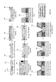
FIGS. 1 a-1 j depict a process for forming an electrical contact and the resultant device according to one aspect of the present invention.
FIGS. 2 a-2 j depict a process for forming an electrical contact and the resultant device according to another aspect of the present invention.
FIGS. 3 a-3 j depict a process for forming an electrical contact and the resultant device according to another aspect of the present invention.
FIGS. 4 a-4 k depict a process for forming an electrical contact and the resultant device according to another aspect of the present invention.
FIGS. 5 a-5 k depict a process for forming an electrical contact and the resultant device according to another aspect of the present invention.
FIGS. 6 a-6 k depict a process for forming an electrical contact and the resultant device according to another aspect of the present invention.
FIGS. 7 a-7 k depict a process for forming an electrical contact and the resultant device according to another aspect of the present invention.
FIGS. 8 a-8 k depict a process for forming an electrical contact and the resultant device according to another aspect of the present invention.
FIGS. 9 a-9 k depict a process for forming an electrical contact and the resultant device according to another aspect of the present invention.
FIGS. 10 a-10 h depict a process for forming an electrical contact and the resultant device according to another aspect of the present invention.
FIG. 11 is an enlarged version of FIG. 10 d.
DETAILED DESCRIPTION
The invention provides a cost-effective and reliable electrical connection for multilayer semiconductor device packages. In the invention, a metallized via makes electrical contact with both a bonding pad and with a thicker conductive material stud beneath the bonding pad. Prior to metallization, the formed via terminates within the thicker conductive material stud to ensure metallization electrical contact over a large region. Various embodiments of this invention are depicted in the following FIGS. 1-10 for different devices and different multilayer configurations; however, all the embodiments share the above features in common.
As used herein, the term “via” is used in a broad sense to mean any opening in an electrical material layer or layers, typically including a path through an insulating material layer, that allows a conductive connection between different layers. Various other similar terms such as trench or channel are encompassed by the term “via” as used in describing the present invention.
Note that in the following embodiments, the conductive material stud is formed on or in a glass wafer; this is because many of the embodiments relate to packaging a CMOS-based image sensor in which a transparent material is used as a cover layer to permit imaging. However, when other devices are formed, such as multilayer semiconductor integrated circuits, the conductive material stud is not required to be formed in a glass layer or in a transparent material layer. That is, the conductive material stud can be formed in any adjacent material layer to facilitate electrical connection with a bonding pad.
The term “conductive material stud” as used herein, relates to a thick plug of conductive material, with a thickness on the order of 5 um to 200 um that is, a thickness substantially larger than the thickness of a conventional bonding pad, which tends to be on the order of 0.5 um to 5 um. The conductive material can be selected from a metal/metal alloy such as gold, copper, aluminum and alloys thereof, conductive metal compounds such as titanium nitride and metal silicides, or transparent conductors such as indium tin oxide.
The following figures depict exemplary embodiments only; as can be seen from the variety of geometries and formation techniques, the invention applies to a large number of conductive material contacts for various electrical devices and device packages.
FIG. 1 depicts a glass substrate 10 (1 a) in which cavities 12 are formed (1 b). The cavities can be formed by mechanical or chemical material removal techniques as are known in the art. Conductive material studs 20 are formed in cavities 12 (1 c) through any known thin film or thick film deposition technique. A semiconductor wafer 30 has one or more electrical devices formed therein (not shown) and a dielectric layer 32 and one or more bonding pads 34 formed thereon. As depicted in FIG. 1 d, the semiconductor wafer 30 is silicon although other semiconductor materials, such as compound semiconductors, can also be used. When the semiconductor wafer is silicon, the dielectric layer 32 is typically silicon dioxide, which can be thermally grown, although other dielectrics can also be used. The semiconductor wafer is bonded to the glass wafer at the projections that hold conductive material studs 20. Any suitable methods, such as direct bonding, can be used to perform the bonding, or other bonding materials can be applied.
The semiconductor wafer 30 is thinned (1 e) followed by trench formation 40 (1 f). A portion of dielectric 32 is removed to expose bonding pad 34 (1 g) followed by a polymer coating 50 (1 h). A via 60 is opened through the polymer coating (1 i). Via 60 passes through bonding pad 34 and terminates in conductive material stud 20 and may be performed by laser drilling or another suitable via formation technique. Since the via terminates within conductive material stud 20, it opens up a large area of conductive material. That is, the entire via tip exposes conductive material. Since this conductive material also contacts bonding pad 34, a reliable electrical contact with the bonding pad can be formed when the via is metallized. Subsequent metallization 70 (1 j) creates a large area of electrical contact with conductive material 20 and bonding pad 34 because the entire via tip terminates in the conductive material stud 20. In comparison with conventional annular contact with a bonding pad only, the contact area between metallization 70 and a conductive material (either bonding pad 34 or stud 20) is approximately 8-10 times greater.
To complete packaging, further processes are performed such as passivation, solder application, dicing into individual devices, encapsulation, etc. as are known in the semiconductor packaging art.
Turning to FIGS. 2-10, it is noted that the last two digits of the element numbers in these figures relate to elements that are substantially similar to elements described with reference to FIG. 1. Thus in FIG. 2 a element 210 is a glass substrate (substantially similar to glass substrate 10 in FIG. 1), 212 are cavities formed in the glass substrate (2 b) with conductive material studs 220 (2 c), etc. Wafer thinning is performed in 2 e. In 2 f, a through silicon via 240 is formed by deep reactive ion etching. Removal of the dielectric/oxide 232 exposes bonding pad 234 (2 g). Polymer coating 250 is formed in 2 h followed by laser drilling a hole 260 through bonding pad 234 and into stud 220, terminating within the stud (2 i). Metallization 270 is coated on the sidewalls of the via and the laser-drilled holes, typically by sputtering (2 j). As with FIG. 1, further packaging processes are performed to create the final device.
In FIG. 3, subparts a-e are substantially similar to a-e of FIGS. 1 and 2. In 3 f, laser drilling is used to form vias 340, and dielectric/oxide removal exposes bonding pad 334 (3 g). Polymer 350 is coated in the via and laser drilling forms hole 360 through the bonding pad 334 and terminating in stud 320 (3 i). Metallization 370 is deposited by sputtering or another suitable technique (3 j) followed by conventional packaging.
In FIG. 4 conductive material studs 420 are formed on the surface of a glass substrate 410 rather than being embedded in a glass cavity (4 a, 4 b). A polymer coating 425 embeds the studs in a polymer layer; subsequent patterning of the polymer layer yields projecting studs encased in polymer. A semiconductor material 430 with dielectric/oxide layer 432 and bonding pads 434 is bonded to the glass substrate with projecting studs in 4 e followed by wafer thinning in 4 f. The remaining portions of FIG. 4 are substantially similar to those of FIG. 1.
Various combinations of the above features can be provided to a device and various process steps can be combined with other process steps in the present invention. For example, in FIG. 5, 5 a-5 f are substantially similar to 4 a-4 f. 5 g-5 k are substantially similar to FIG. 2. Similarly, in FIG. 6, 6 a-6 f are substantially similar to 4 a-4 f while 6 g-6 j are substantially similar to 3 f-3 j.
In FIG. 7, a CMOS image sensor (CIS) 730 is provided (7 a) having bonding pads 734 formed in dielectric layer 732 (e.g., silicon oxide or a polymer) and conductive material studs 720 are formed over the dielectric/oxide layer 732 having bonding pads 734 formed therein or thereon (7 b). A polymer coating 725 embeds the studs followed by polymer patterning to yield stud projections on the CIS wafer. A glass wafer 710 is bonded to the CIS/stud projection combination followed by trench etching 740 and oxide removal exposing bonding pads 734 (7 g-7 h). A polymer coating 750 is deposited (7 i) followed by laser drilling forming holes 760 that terminate in the stud. Metallization 770 covers the trench and both holes, followed by metal removal between the adjacent holes (for electrical isolation).
In FIG. 8, 8 a-8 f are substantially similar to 7 a-7 f. FIG. 8 g-8 k are substantially similar to 2 f-2 j. In FIG. 9, 9 a-9 f are substantially similar to 7 a-7 f. FIG. 9 g-9 k are substantially similar to 3 f-3 j.
FIG. 10 depicts formation of a backside illuminated (BSI) CIS device package. A handling glass/silicon substrate 1010 is provided with conductive material stud projections 1020 which are embedded in a polymer layer 1025 (10 a-10 c). A BSI-CIS wafer 1030 with a dielectric/oxide 1032 and bonding pads 1034 and cover glass 1036 and lenses 1038 is bonded to the handling substrate plus metal studs embedded in polymer formed in 10 a-10 c. Vias 1040 are formed in the handling substrate in 10 e followed by polymer deposition 1050 laser drilling to form contact vias 1060 and metallization 1070.
The foregoing has outlined the features and technical advantages of the present invention. It should be appreciated by those skilled in the art that the conception and specific embodiment disclosed may be readily utilized as a basis for modifying or designing other structures for carrying out the same purposes of the present invention. It should also be realized by those skilled in the art that such equivalent constructions do not depart from the spirit and scope of the invention as set forth in the appended claims.

Claims (20)

The invention claimed is:
1. A microelectronic device package including one or more electrical contacts comprising:
a semiconductor material layer having one or more electrical devices fabricated therein and having an electrical contact pad positioned therein;
a layer positioned adjacent to the semiconductor material layer, the layer including a conducting material stud embedded in or formed on the layer or bonded to the layer, wherein the conducting material stud is positioned beneath the electrical contact pad;
a via formed through at least a portion of the semiconductor material layer and through the electrical contact pad and into the conducting material stud, wherein the conducting material stud relates to a thick plug of conductive material with a thickness on the order of 5 um to 200 um which is the thickness substantially larger than the thickness of the electrical contact pad, and the conducting material stud, positioned beneath the electrical contact pad, is in physical and electrical contact with the electrical contact pad, and the tip of the via terminates within at least a portion of the conducting material stud opening up an area of the conductive material performed by a via formation technique such that the entire via tip exposes the area of the conductive material of the conducting material stud, wherein the formed via terminates within the conducting material stud to ensure metallization of the electrical contact over a large region; and
a metallization layer disposed in the via such that the metallization layer contacts the electrical contact pad and the area of the conductive material of the conducting material stud through the via tip to have electrical contact with both the electrical contact pad and the conductive material stud, wherein the metallization layer, the electrical contact pad and the conducting material stud are in physical and electrical contact among each other.
2. A multilayer microelectronic device package including one or more vertical electrical contacts according to claim 1 wherein the conducting material stud comprises a metal, a metal alloy, or a conductive metal compound.
3. A multilayer microelectronic device package including one or more vertical electrical contacts according to claim 1 wherein the via is formed by laser drilling.
4. A multilayer microelectronic device package including one or more vertical electrical contacts according to claim 1 wherein the via is formed by mechanical material removal.
5. A multilayer microelectronic device package including one or more vertical electrical contacts according to claim 1 wherein the semiconductor material is silicon.
6. A multilayer microelectronic device package including one or more vertical electrical contacts according to claim 1 wherein a CMOS imaging device is formed in the semiconductor material layer.
7. A multilayer microelectronic device package including one or more vertical electrical contacts according to claim 1 wherein the stud-containing layer is a glass layer.
8. A multilayer microelectronic device package including one or more vertical electrical contacts according to claim 1 wherein the adjacent layer with conducting material stud is formed on the semiconductor material layer.
9. A multilayer microelectronic device package including one or more vertical electrical contacts according to claim 1 wherein the adjacent layer with conducting material stud is bonded to the semiconductor layer.
10. A multilayer microelectronic device package including one or more vertical electrical contacts according to claim 1 wherein the thickness of the electrical contact pad is on the order of 0.5 um to 5 um.
11. A multilayer microelectronic device package including one or more vertical electrical contacts according to claim 1 wherein the via is positioned in a trench formed by trench etching of the semiconductor material layer.
12. A multilayer microelectronic device package including one or more vertical electrical contacts according to claim 1 wherein the via is positioned in a through silicon via formed by deep reactive ion etching or laser drilling of the semiconductor material layer.
13. A multilayer microelectronic device package including one or more vertical electrical contacts according to claim 1 further comprising:
a polymer coating positioned between the layer and the metallization layer.
14. A microelectronic device package including one or more electrical contacts comprising:
a semiconductor material layer having one or more electrical devices fabricated therein and having an electrical contact pad positioned therein;
a layer positioned adjacent to the semiconductor material layer, the layer including a conducting material stud embedded in or formed on the layer or bonded to the layer, wherein the conducting material stud is positioned beneath the electrical contact pad;
a via formed through at least a portion of the semiconductor material layer and through the electrical contact pad and into the conducting material stud, wherein the conducting material stud relates to a thick plug of conductive material with a thickness on the order of 5 um to 200 um which is the thickness substantially larger than the thickness of the electrical contact pad being on the order of 0.5 um to 5 um, and the conducting material stud, positioned beneath the electrical contact pad, is in physical and electrical contact with the electrical contact pad, and the tip of the via terminates within at least a portion of the conducting material stud opening up an area of the conductive material performed by a via formation technique such that the entire via tip exposes the area of the conductive material of the conducting material stud and the electrical contact pad, wherein the formed via terminates within the conducting material stud to ensure metallization of the electrical contact over a large region; and
a metallization layer disposed in the via such that the metallization layer contacts the electrical contact pad and the area of the conductive material of the conducting material stud through the via tip to have electrical contact with both the electrical contact pad and the conductive material stud, wherein the metallization layer, the electrical contact pad and the conducting material stud are in physical and electrical contact among each other.
15. A multilayer microelectronic device package including one or more vertical electrical contacts according to claim 14 wherein the conducting material stud comprises a metal, a metal alloy, or a conductive metal compound.
16. A multilayer microelectronic device package including one or more vertical electrical contacts according to claim 14 wherein the via is formed by laser drilling.
17. A multilayer microelectronic device package including one or more vertical electrical contacts according to claim 14 wherein the via is formed by mechanical material removal.
18. A multilayer microelectronic device package including one or more vertical electrical contacts according to claim 14 wherein the semiconductor material is silicon.
19. A multilayer microelectronic device package including one or more vertical electrical contacts according to claim 14 wherein a CMOS imaging device is formed in the semiconductor material layer.
20. A multilayer microelectronic device package including one or more vertical electrical contacts according to claim 14 wherein the stud-containing layer is a glass layer.
US13/354,302 2012-01-19 2012-01-19 Increased surface area electrical contacts for microelectronic packages Expired - Fee Related US8772930B2 (en)

Priority Applications (2)

Application Number Priority Date Filing Date Title
US13/354,302 US8772930B2 (en) 2012-01-19 2012-01-19 Increased surface area electrical contacts for microelectronic packages
CN201210057891.5A CN102646655B (en) 2012-01-19 2012-03-07 Structure for increasing electric contact surface area in micro-electronic packaging

Applications Claiming Priority (1)

Application Number Priority Date Filing Date Title
US13/354,302 US8772930B2 (en) 2012-01-19 2012-01-19 Increased surface area electrical contacts for microelectronic packages

Publications (2)

Publication Number Publication Date
US20130187267A1 US20130187267A1 (en) 2013-07-25
US8772930B2 true US8772930B2 (en) 2014-07-08

Family

ID=46659396

Family Applications (1)

Application Number Title Priority Date Filing Date
US13/354,302 Expired - Fee Related US8772930B2 (en) 2012-01-19 2012-01-19 Increased surface area electrical contacts for microelectronic packages

Country Status (2)

Country Link
US (1) US8772930B2 (en)
CN (1) CN102646655B (en)

Citations (9)

* Cited by examiner, † Cited by third party
Publication number Priority date Publication date Assignee Title
US20070099395A1 (en) * 2005-11-03 2007-05-03 Uppili Sridhar Wafer level packaging process
US7274101B2 (en) * 2004-06-30 2007-09-25 Fujikura Ltd. Semiconductor package and method for manufacturing the same
US20080237766A1 (en) * 2005-02-02 2008-10-02 Ki-Hong Kim Image sensing devices including image sensor chips, image sensor package modules employing the image sensing devices, electronic products employing the image sensor package modules, and methods of fabricating the same
US20080284041A1 (en) 2007-05-18 2008-11-20 Samsung Electronics Co., Ltd. Semiconductor package with through silicon via and related method of fabrication
US20090050996A1 (en) * 2007-08-24 2009-02-26 Xintec Inc. Electronic device wafer level scale packages and fabrication methods thereof
TW200937605A (en) 2007-12-27 2009-09-01 Toshiba Kk Semiconductor package including through-hole electrode and light-transmitting substrate
US20100230795A1 (en) * 2009-03-13 2010-09-16 Tessera Technologies Hungary Kft. Stacked microelectronic assemblies having vias extending through bond pads
CN101847664A (en) 2010-03-15 2010-09-29 香港应用科技研究院有限公司 Electron device package and method for manufacturing same
US20110278734A1 (en) * 2010-03-11 2011-11-17 Yu-Lin Yen Chip package and method for forming the same

Patent Citations (13)

* Cited by examiner, † Cited by third party
Publication number Priority date Publication date Assignee Title
US7274101B2 (en) * 2004-06-30 2007-09-25 Fujikura Ltd. Semiconductor package and method for manufacturing the same
US7964926B2 (en) * 2005-02-02 2011-06-21 Samsung Electronics Co., Ltd. Image sensing devices including image sensor chips, image sensor package modules employing the image sensing devices, electronic products employing the image sensor package modules, and methods of fabricating the same
US20080237766A1 (en) * 2005-02-02 2008-10-02 Ki-Hong Kim Image sensing devices including image sensor chips, image sensor package modules employing the image sensing devices, electronic products employing the image sensor package modules, and methods of fabricating the same
US7393758B2 (en) * 2005-11-03 2008-07-01 Maxim Integrated Products, Inc. Wafer level packaging process
US20070099395A1 (en) * 2005-11-03 2007-05-03 Uppili Sridhar Wafer level packaging process
US20080284041A1 (en) 2007-05-18 2008-11-20 Samsung Electronics Co., Ltd. Semiconductor package with through silicon via and related method of fabrication
US20090050996A1 (en) * 2007-08-24 2009-02-26 Xintec Inc. Electronic device wafer level scale packages and fabrication methods thereof
TW200937605A (en) 2007-12-27 2009-09-01 Toshiba Kk Semiconductor package including through-hole electrode and light-transmitting substrate
US7808064B2 (en) * 2007-12-27 2010-10-05 Kabushiki Kaisha Toshiba Semiconductor package including through-hole electrode and light-transmitting substrate
US20090283847A1 (en) * 2007-12-27 2009-11-19 Atsuko Kawasaki Semiconductor package including through-hole electrode and light-transmitting substrate
US20100230795A1 (en) * 2009-03-13 2010-09-16 Tessera Technologies Hungary Kft. Stacked microelectronic assemblies having vias extending through bond pads
US20110278734A1 (en) * 2010-03-11 2011-11-17 Yu-Lin Yen Chip package and method for forming the same
CN101847664A (en) 2010-03-15 2010-09-29 香港应用科技研究院有限公司 Electron device package and method for manufacturing same

Non-Patent Citations (1)

* Cited by examiner, † Cited by third party
Title
Office Action issued from the State Intellectual Property Office of the People's Republic of China on Mar. 3, 2014.

Also Published As

Publication number Publication date
US20130187267A1 (en) 2013-07-25
CN102646655B (en) 2014-10-22
CN102646655A (en) 2012-08-22

Similar Documents

Publication Publication Date Title
TWI629759B (en) Chip package and method for forming the same
US10157811B2 (en) Chip package and method for forming the same
US9859322B2 (en) Methods and apparatus for glass removal in CMOS image sensors
US9177919B2 (en) Chip package and method for forming the same
US8860217B1 (en) Electronic device package
TWI647799B (en) Semiconductor package and method of manufacturing same
US10153237B2 (en) Chip package and method for forming the same
KR100659625B1 (en) Semiconductor device and method for manufacturing the same
US20070126085A1 (en) Semiconductor device and method of manufacturing the same
US9379072B2 (en) Chip package and method for forming the same
TWI717846B (en) Chip package and method for forming the same
TW201110294A (en) Chip package and fabrication method thereof
US9059180B2 (en) Thick bond pad for chip with cavity package
CN105742193A (en) Wafer and Wafer Bonding Process and Structures
US8772930B2 (en) Increased surface area electrical contacts for microelectronic packages
US20200185345A1 (en) Semiconductor device
US11973095B2 (en) Method for forming chip package with second opening surrounding first opening having conductive structure therein

Legal Events

Date Code Title Description
AS Assignment

Owner name: HONG KONG APPLIED SCIENCE AND TECHNOLOGY RESEARCH

Free format text: ASSIGNMENT OF ASSIGNORS INTEREST;ASSIGNORS:LAW, PUI CHUNG SIMON;YANG, DAN;SHI, XUNQING;REEL/FRAME:027564/0145

Effective date: 20120119

STCF Information on status: patent grant

Free format text: PATENTED CASE

MAFP Maintenance fee payment

Free format text: PAYMENT OF MAINTENANCE FEE, 4TH YEAR, LARGE ENTITY (ORIGINAL EVENT CODE: M1551)

Year of fee payment: 4

FEPP Fee payment procedure

Free format text: MAINTENANCE FEE REMINDER MAILED (ORIGINAL EVENT CODE: REM.); ENTITY STATUS OF PATENT OWNER: LARGE ENTITY

LAPS Lapse for failure to pay maintenance fees

Free format text: PATENT EXPIRED FOR FAILURE TO PAY MAINTENANCE FEES (ORIGINAL EVENT CODE: EXP.); ENTITY STATUS OF PATENT OWNER: LARGE ENTITY

STCH Information on status: patent discontinuation

Free format text: PATENT EXPIRED DUE TO NONPAYMENT OF MAINTENANCE FEES UNDER 37 CFR 1.362

FP Lapsed due to failure to pay maintenance fee

Effective date: 20220708