US8773178B2 - Coupling arrangement for phantom-mode transmission - Google Patents
Coupling arrangement for phantom-mode transmission Download PDFInfo
- Publication number
- US8773178B2 US8773178B2 US13/816,856 US201113816856A US8773178B2 US 8773178 B2 US8773178 B2 US 8773178B2 US 201113816856 A US201113816856 A US 201113816856A US 8773178 B2 US8773178 B2 US 8773178B2
- Authority
- US
- United States
- Prior art keywords
- differential
- mode
- pair
- common
- coupling
- Prior art date
- Legal status (The legal status is an assumption and is not a legal conclusion. Google has not performed a legal analysis and makes no representation as to the accuracy of the status listed.)
- Expired - Fee Related
Links
Images


Classifications
-
- H—ELECTRICITY
- H04—ELECTRIC COMMUNICATION TECHNIQUE
- H04L—TRANSMISSION OF DIGITAL INFORMATION, e.g. TELEGRAPHIC COMMUNICATION
- H04L25/00—Baseband systems
- H04L25/02—Details ; arrangements for supplying electrical power along data transmission lines
-
- H—ELECTRICITY
- H04—ELECTRIC COMMUNICATION TECHNIQUE
- H04L—TRANSMISSION OF DIGITAL INFORMATION, e.g. TELEGRAPHIC COMMUNICATION
- H04L5/00—Arrangements affording multiple use of the transmission path
- H04L5/20—Arrangements affording multiple use of the transmission path using different combinations of lines, e.g. phantom working
-
- H—ELECTRICITY
- H04—ELECTRIC COMMUNICATION TECHNIQUE
- H04L—TRANSMISSION OF DIGITAL INFORMATION, e.g. TELEGRAPHIC COMMUNICATION
- H04L25/00—Baseband systems
- H04L25/02—Details ; arrangements for supplying electrical power along data transmission lines
- H04L25/0264—Arrangements for coupling to transmission lines
- H04L25/0272—Arrangements for coupling to multiple lines, e.g. for differential transmission
- H04L25/0274—Arrangements for ensuring balanced coupling
-
- H—ELECTRICITY
- H04—ELECTRIC COMMUNICATION TECHNIQUE
- H04L—TRANSMISSION OF DIGITAL INFORMATION, e.g. TELEGRAPHIC COMMUNICATION
- H04L25/00—Baseband systems
- H04L25/02—Details ; arrangements for supplying electrical power along data transmission lines
- H04L25/0264—Arrangements for coupling to transmission lines
- H04L25/0272—Arrangements for coupling to multiple lines, e.g. for differential transmission
- H04L25/0276—Arrangements for coupling common mode signals
-
- H—ELECTRICITY
- H04—ELECTRIC COMMUNICATION TECHNIQUE
- H04L—TRANSMISSION OF DIGITAL INFORMATION, e.g. TELEGRAPHIC COMMUNICATION
- H04L25/00—Baseband systems
- H04L25/02—Details ; arrangements for supplying electrical power along data transmission lines
- H04L25/0264—Arrangements for coupling to transmission lines
- H04L25/028—Arrangements specific to the transmitter end
-
- H—ELECTRICITY
- H04—ELECTRIC COMMUNICATION TECHNIQUE
- H04L—TRANSMISSION OF DIGITAL INFORMATION, e.g. TELEGRAPHIC COMMUNICATION
- H04L25/00—Baseband systems
- H04L25/02—Details ; arrangements for supplying electrical power along data transmission lines
- H04L25/0264—Arrangements for coupling to transmission lines
- H04L25/0298—Arrangement for terminating transmission lines
Definitions
- the present invention relates to phantom-mode transmission over a wired loop plant comprising a first wire pair and a second wire-pair, and more specifically to a coupling arrangement for coupling transmitters for phantom-mode transmission over the wired loop plant.
- a central office equipment such as a Digital Subscriber Line Access Multiplexer (DSLAM)
- DSL bonding provides DSL services to a subscriber over a first and a second twisted pair (also called DSL bonding), as well as over a virtual (or phantom) channel defined by the difference in common-mode voltages between the first and second twisted pairs.
- DSL bonding provides DSL services to a subscriber over a first and a second twisted pair (also called DSL bonding), as well as over a virtual (or phantom) channel defined by the difference in common-mode voltages between the first and second twisted pairs.
- CPE Customer Premises Equipment
- a third transformer is coupled to the center taps of the secondary windings of the first and second transformer to create said phantom channel.
- the first and second twisted pairs may be used for downstream communication, while upstream communications are transmitted via the phantom channel.
- all three available channels can be used in frequency division duplexing, i.e. for both upstream and downstream communication.
- phantom-mode transmission An alternative embodiment of phantom-mode transmission is described in US patent application 2006/268966.
- the phantom mode is defined as being the differential signal between a twisted pair and a common ground.
- providing such phantom channel derived from a common ground is known to cause a large amount of egress noise and to be highly susceptible to ingress.
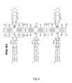
- FIGS. 1 and 2 The prior art coupling arrangement for phantom-mode transmission is now described with reference to FIGS. 1 and 2 wherein:
- FIG. 1 represents a typical coupling arrangement for coupling a transmitter to a transmission line
- FIG. 2 represents a typical coupling arrangement for coupling three transmitters over two transmission lines using phantom-mode transmission.
- FIG. 1 a typical coupling arrangement for coupling a transmitter A to a transmission line L 1 .
- the transmitter A comprises, as an illustrative embodiment, a Digital Signal Processor (DSP) DSPA for digitally encoding a data stream into data symbols to be transmitted over the line L 1 .
- the data stream is typically encoded in the frequency domain over a plurality of carriers (or tones), e.g. by means of Quadrature Amplitude Modulation (QAM).
- the transmit data symbols are fed towards a Digital-to-Analog Converter (DAC) DACA as digital time-domain samples.
- DAC Digital-to-Analog Converter
- the time-domain samples are fed through a data bus comprising n lines, with n denoting the number of bits used for quantifying the individual samples.
- the DAC DACA converts the digital samples into an analogue differential signal comprising two complementary and fully-balanced signals denoted as +VA and ⁇ VA.
- the differential signal is fed to a differential amplifier AMPA with high Common Mode Rejection Ratio (CMRR) through input terminals 1 and 2 .
- CMRR Common Mode Rejection Ratio
- the differential amplifier AMPA amplifies the difference between the two complementary signals +VA and ⁇ VA, namely 2 VA, and outputs two amplified complementary and fully-balanced signals +VA′ and ⁇ VA′ through output terminals 3 and 4 .
- the coupling unit COUP 1 A is a specific transformer arrangement comprising two terminals 101 and 102 coupled to the differential outputs 3 and 4 of the differential amplifier AMPA, and two terminals 103 and 104 coupled to the line L 1 .
- the line L 1 is a twisted copper pair comprising a first and second wire indistinctly referred to as the tip and ring of the line L 1 , and respectively denoted as L 1 -T and L 1 -R.
- the coupling unit COUP 1 A comprises a first primary winding W 1 A, a first capacitor C 1 A and a second primary winding W 2 A serially coupled between the terminals 101 and 102 , and a first secondary winding W 3 A, a second capacitor C 2 A and a second secondary winding W 4 A serially coupled between the terminals 103 and 104 .
- the windings W 1 A, W 2 A, W 3 A and W 4 A are magnetically coupled to each other.
- the primary windings W 1 A and W 2 A are matched to each other, and so are the secondary windings W 3 A and W 4 A.
- the coupling unit COUP 1 A is primarily for passing the amplified differential signal towards the line L 1 , and yields two complementary and fully-balanced signals +VA′′ and ⁇ VA′′ over the line L 1 .
- the coupling unit COUP 1 A is for further isolating the transceiver circuitry from any DC component present over the line L 1 .
- any common-mode signals present on the differential amplifier output (mostly on account of component mismatches within the differential amplifier) is fully rejected by the transformer arrangement as they do not yield any current over the primary windings.
- the combination of the capacitor CIA with the mutually-coupled inductors W 1 A/W 3 A and W 2 A/W 4 A and the further capacitor C 2 A forms a third-order high-pass filter, e.g. for filtering out any unwanted signals present in the Plain Old Telephony Service (POTS) frequency band.
- POTS Plain Old Telephony Service
- FIG. 2 a typical coupling arrangement for coupling three transmitters A, B and C over two transmission lines L 1 and L 2 using phantom-mode transmission.
- the transmitters A and B are respectively coupled to the lines L 1 and L 2 as aforementioned in FIG. 1 with alike reference numerals.
- the coupling unit COUP 1 A has been slightly modified with the single capacitor C 2 A, respectively C 2 B, replaced by two serially-coupled matched capacitors with total equivalent capacitance, and with a further terminal 5 , respectively 15 , coupled to the inter-connection track between the two capacitors.
- the resulting coupling units are denoted as COUP 1 A′ and COUP 1 B′ respectively.
- the third transmitter C produces two complementary and fully-balanced signal +VC and ⁇ VC to be added as common-mode signals to both the tip and ring of lines L 1 and L 2 respectively.
- the terminals 123 and 124 of the coupling unit COUP 1 C are connected to the terminals 5 and 15 respectively, and evenly add to both the tip and ring of the lines L 1 and L 2 by means of the two serial capacitors, thereby yielding +VA′′+VC′′ and ⁇ VA′′+VC′′ on line L 1 , and +VB′′ ⁇ VC′′ and ⁇ VB′′ ⁇ VC′′ on line L 2 .
- the disclosed coupling arrangement is disadvantageous in that all those components require board space, limiting the total number of lines that can be equipped on a line termination unit, and in that the total Bill Of Material (BOM) for phantom-mode transmission is increased.
- BOM Bill Of Material
- a coupling arrangement for coupling transmitters to a wired loop plant comprises:
- the total power consumed by such a coupling arrangement is substantially decreased.
- said first and second common signals correspond to a third differential-mode signal from a third transmitter.
- the adders have a first input terminal coupled to an output terminal of the regular transmitter and a second input terminal coupled to an output terminal of the phantom-mode transmitter. Both the regular and phantom-mode transmitters produce fully balanced differential signals.
- said first and second adders form part of said first and second transmitters respectively, and said first and second transmitters are further configured to directly output said first and second common-and-differential-mode signals respectively.
- the output of the phantom-mode transmitter is added in the digital domain to the differential-mode signal as a common-mode signal, thereby yielding unbalanced signals at the outputs of the first and second transmitters comprising a common-mode component for phantom-mode transmission.
- This embodiment is particularly advantageous in that the DAC stage is no longer needed for the phantom-mode transmitter, and in that the BOM and the consumed power are reduced at a further extent.
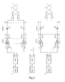
- FIG. 3 represents a first coupling arrangement according to the invention
- FIG. 4 represents a second coupling arrangement according to the invention.
- FIG. 3 a first coupling arrangement according to the invention with:
- the coupling arrangement may also comprise corresponding receive paths (not shown) for receiving both differential-mode and common-mode signals from the lines L 1 and L 2 , and for feeding the received signals to respective receivers for further handling (amplifying, demodulating, decoding, etc).
- the three transmitters A, B and C are shown as comprising DSPs DSPA, DSPB and DSPC respectively coupled to DACs DACA, DACB and DACC, but the present invention should not be limited to that specific embodiment and may apply indistinctly to alternative analog or digital transmitter implementations.
- the transmitters A, B and C output differential-mode and fully-balanced signals (+VA(t), ⁇ VA(t)), (+VB(t), ⁇ VB(t)) and (+VC(t), ⁇ VC(t)) respectively onto output terminal pairs, wherein t denotes the time-dependence of the signals (the time dependence will be omitted in the following).
- the coupling arrangement comprises the following functional blocks:
- the two output terminals of the transmitter A are coupled to an input terminal of the two adders ⁇ 1 A and ⁇ 2 A respectively.
- the two output terminals of the transmitter B are coupled to an input terminal of the two adders ⁇ 1 B and ⁇ 2 B respectively.
- the first output terminal of the transmitter C is coupled to an input terminal of the two adders ⁇ 1 A and ⁇ 2 A, and the second output terminal of the transmitter C is coupled to an input terminal of the two adders ⁇ 1 B and ⁇ 2 B.
- the adders ⁇ 1 A, ⁇ 2 A, ⁇ 1 B and ⁇ 2 B are for adding together the signals present on their two input terminals, and to output the sum of the two signals onto the output terminal. Implementations of the adders ⁇ 1 A, ⁇ 2 A, ⁇ 1 B and ⁇ 2 B by means of basic electronics are well know in the art.
- the output terminals of the adders ⁇ 1 A, ⁇ 2 A, ⁇ 1 B and ⁇ 2 B are respectively coupled to the input terminals 1 , 2 , 11 and 12 of the amplification units AMP 2 A and AMP 2 B, and put out signals +VA+VC, ⁇ VA+VC, +VB ⁇ VC and ⁇ VB ⁇ VC respectively.
- the output terminals 3 , 4 , 13 and 14 of the amplification units AMP 2 A and AMP 2 B are respectively coupled to the input terminals 101 , 102 , 111 and 112 of the coupling units COUP 2 A and COUP 2 B.
- the output terminals 103 and 104 of the coupling unit COUP 2 A are respectively coupled to the tip L 1 -T and the ring L 1 -R of the line L 1 .
- the output terminals 113 and 114 of the coupling unit COUP 2 A are respectively coupled to the tip L 2 -T and ring L 2 -R of the line L 2 .
- the amplification unit AMP 2 A and AMP 2 B are configured to amplify both common-mode and differential-mode signals applied to their respective pair of input terminals ( 1 , 2 ) and ( 11 , 12 ). This is achieved by individually amplifying each signal component with substantially the same amplification gain.
- the first amplification unit AMP 2 A comprises a first amplifier AMP 2 A 1 between the input terminal 1 and the output terminal 3 for amplifying the signal +VA+VC put out by the first adder ⁇ 1 A, thereby yielding +VA′+VC′ as amplified signal, and a second amplifier AMP 2 A 2 between the input terminal 2 and the output terminal 4 for amplifying the signal ⁇ VA+VC put out by the second adder ⁇ 2 A, thereby yielding ⁇ VA′+VC′ as amplified signal.
- the second amplification unit AMP 2 B comprises a third amplifier AMP 2 B 1 between the input terminal 11 and the output terminal 13 for amplifying the signal +VB ⁇ VC put out by the third adder ⁇ 1 B, thereby yielding +VB′ ⁇ VC′ as amplified signal, and a fourth amplifier AMP 2 B 2 between the input terminal 12 and the output terminal 14 for amplifying the signal ⁇ VB ⁇ VC put out by the fourth adder ⁇ 2 B, thereby yielding ⁇ VB′ ⁇ VC′ as amplified signal.
- V 1 ( t ) and V 2 ( t ) denote any two signals, each one driving one wire of a wire pair, such as the tip and the ring of a subscriber loop.
- Vd(t) Vc ( t )+ Vd ( t )/2
- V 2( t ) Vc ( t ) ⁇ Vd ( t )/2
- Vd ( t ) V 1( t ) ⁇ V 2( t ) (3)
- Vc ⁇ ( t ) V ⁇ ⁇ 1 ⁇ ( t ) + V ⁇ ⁇ 2 ⁇ ( t ) 2 . ( 4 )
- G denote the common gain factor of the amplifiers AMP 2 A 1 , AMP 2 A 2 , AMP 2 B 1 and AMP 2 B 2 .
- V 1 c , V 1 d ) and (V 1 c ′, V 1 d ′) denote the common-mode and differential-mode signals respectively present on the input terminal pair ( 1 , 2 ) and the output terminal pair ( 3 , 4 ) of the first amplification unit AMP 2 A.
- V 2 c , V 2 d ) and (V 2 c ′, V 2 d ′) denote the common-mode and differential-mode signals respectively present on the input terminal pair ( 11 , 12 ) and the output terminal pair ( 13 , 14 ) of the second amplification unit AMP 2 B.
- both common-mode and differential-mode signals present on the input terminal pairs of the amplification unit AMP 2 A and AMP 2 B are amplified with the same gain G.
- the gain factors of the individual amplifiers AMP 2 A 1 , AMP 2 A 2 , AMP 2 B 1 and AMP 2 B 2 are not necessarily equal, e.g. on account of component mismatches, but they should match as close as possible so as to achieve high common-mode-to-differential-mode and differential-mode-to-common-mode rejection ratios.
- G 1 and G 2 denote the respective gain factors of the amplifiers AMP 2 A 1 and AMP 2 A 2 .
- G 2 G 1 + ⁇ G, and:
- the differential-mode voltage V 1 d ′ output by the amplification unit AMP 2 A depends on both the differential-mode and common-mode input voltages.
- the common-mode voltage V 1 c ′ output by the amplification unit AMP 2 A depends on both the common-mode and differential-mode input voltages.
- ⁇ G i.e. the gain mismatching between the two amplifiers AMP 2 A 1 and AMP 2 A 2 , so as to decrease the common-mode-to-differential-mode and differential-mode-to-common-mode couplings of the amplification unit AMP 2 A.
- the coupling units COUP 2 A and COUP 2 B are configured for passing both common-mode and differential-mode signals from their input terminals towards their output terminals. This is achieved by means of capacitive coupling.
- the coupling unit COUP 2 A comprises a first capacitor C 3 A between the input terminal 101 and the output terminal 103 , and a second capacitor C 4 A between the input terminal 102 and the output terminal 104 .
- the coupling unit COUP 2 B comprises a third capacitor C 3 B between the input terminal 111 and the output terminal 113 , and a second capacitor C 4 B between the input terminal 112 and the output terminal 114 .
- the capacitors C 3 A, C 4 A, C 3 B and C 4 B behave as a first-order high-pass filter for the respective signals +VA′+VC′, ⁇ VA′+VC′, +VB′ ⁇ VC′ and ⁇ VB′ ⁇ VC′ applied to the respective input terminals 101 , 102 , 111 and 112 , thereby yielding filtered common-mode and differential-mode signals +VA′′+VC′′, ⁇ VA′′+VC′′, +VB′′ ⁇ VC′′ and ⁇ VB′′ ⁇ VC′′ on the respective output terminals 103 , 104 , 113 and 114 .
- Additional components such as resistors and/or capacitors and/or inductors, can be added to the capacitors C 3 A, C 4 A, C 3 B and C 4 B, to improve the filter characteristics, e.g. to design a third-order high-pass filter for filtering out any unwanted low-frequency signal that might be present in the POTS band because of non-linearity in e.g. the amplification units AMP 2 A and AMP 2 B.
- the impairments of the amplification and coupling stages can be dealt with by careful hardware design with perfectly matched components, and/or by means of a feedback loop or compensation circuit.
- That part of the phantom channel signal that ultimately leaks into the regular channel on account of the aforementioned common-mode-to-differential-mode and differential-mode-to-common-mode couplings can be further canceled by signal pre-coding or signal post-processing over the regular channel, and vice-versa.
- a method for crosstalk cancellation between the regular and phantom channels is described in EP patent application 2091196 entitled “ Method and Apparatus for DSL Communication”.
- FIG. 4 a second embodiment of a coupling arrangement according to the invention, wherein the adders ⁇ 1 A, ⁇ 2 A, ⁇ 1 B and ⁇ 2 B have been advantageously moved within the transmitters A and B, and more specifically within the DACs DACA and DACB.
- the DAC of the transmitter C is no longer needed and can be taken out from the PBA, thereby saving extra cost.
- the DAC DACA comprises two input terminals and two output terminals, with a first input terminal coupled to DSPA's output and fed with first digital samples to be output as differential-mode signal on the output terminal pair, and a second input terminal coupled to DSPC's output and fed with second digital samples to be output as common-mode signal on the output terminal pair.
- the DAC DACB comprises two input terminals and two output terminals, with a first input terminal coupled to DSPB's output and fed with first digital samples to be output as differential-mode signal on the output terminal pair, and a second input terminal coupled to DSPC's output and fed with second digital samples to be inverted and output as common-mode signal on the output terminal pair.
- the DAC DACA is configured to produce two complementary digital signals from first samples, namely +VA and ⁇ VA, and to add second digital samples namely +VC, to each complementary digital signals before analog-to-digital conversion, thereby yielding an unbalanced and asymmetrical signal on the output terminal pair, namely +VA+VC and ⁇ VA+VC.
- the DAC DACB is configured to produce two complementary digital signals from first samples, namely +VB and ⁇ VB, and to invert and add second digital samples, namely ⁇ VC, to each complementary digital signals before analog-to-digital conversion, thereby yielding an unbalanced and asymmetrical signal on the output terminal pair, namely +VB ⁇ VC and ⁇ VB ⁇ VC.
- the amplification units AMP 2 A and AMP 2 B and the coupling units COUP 2 A and COUP 2 B are left unchanged.
- the power saving achieved by reducing the number of amplifiers from 3 down to 2 does however not save 33% of the power consumed by the amplifiers.
- the two remaining amplifiers (AMP 1 A and AMP 1 B) generating both the differential-mode and common-mode mode signals need to output more power and hence consume more power.
- the supply voltage of a line driver must be sufficiently high to deliver crest peaks up to 5 or 6 times the Root Mean Square (RMS) power.
- RMS Root Mean Square
- crest peaks are very rare, and probability that they will occur simultaneously on the differential channel ((+VA′, ⁇ VA′) or (VB′, ⁇ VB′)) and the phantom channel ((+VC′, ⁇ VC′)) can be ignored in function of the desired Bit Error Rate (BER).
- the power supply of an amplifier outputting both differential-mode and common-mode signals can therefore be limited to the supply voltage required to generate the sum of the RMS powers plus e.g. one crest peak. This would be around 120% of the supply voltage that would be required for a differential-mode signal only, and would yield a power reduction of minimum 20% for the amplifier section only. Also, a further power reduction can be achieved by eliminating the third DAC (DACC) as shown in the embodiment of FIG. 4 .
- DACC third DAC
- a coupling arrangement according to the invention typically forms part of a line termination unit, which is a piece of equipment whereat transmission lines from subscriber premises terminate.
- This piece of equipment forms part of an access node for providing network access to subscribers.
- access nodes are a DSLAM, an Ethernet access bridge, an IP access or edge router, etc.
- the access node may reside at a central location (e.g., a central office), or at a remote location closer to subscriber premises (e.g., a street cabinet)
- a device A coupled to a device B should not be limited to devices or systems wherein an output of device A is directly connected to an input of device B, and/or vice-versa. It means that there exists a path between an output of A and an input of B, and/or vice-versa, which may be a path including other devices or means.
- DSP digital signal processor
- ASIC application specific integrated circuit
- FPGA field programmable gate array
- Other hardware, conventional and/or custom, such as read only memory (ROM), random access memory (RAM), and non volatile storage, may also be included.
Abstract
Description
-
- a first amplification unit with a first pair of input terminals to be fed with a first differential-mode signal from a first transmitter, and configured to output a first amplified differential-mode signal onto a first pair of output terminals,
- a second amplification unit with a second pair of input terminals to be fed with a second differential-mode signal from a second transmitter, and configured to output a second amplified differential-mode signal onto a second pair of output terminals,
- a first coupling unit with a third pair of input terminals coupled to said first pair of output terminals, and configured to pass said first amplified differential-mode signal towards a third pair of output terminals to be coupled to a first wire pair,
- a second coupling unit with a fourth pair of input terminals coupled to said second pair of output terminals, and configured to pass said second amplified differential-mode signal towards a fourth pair of output terminals to be coupled to a second wire pair,
wherein said coupling arrangement further comprises: - a first adder configured to add a first common signal to said first differential-mode signal, thereby yielding a first common-and-differential-mode signal,
- a second adder configured to add a second common signal that is complementary of said first common signal to said second differential-mode signal, thereby yielding a second common-and-differential-mode signal,
wherein said first and second amplification units are further configured to individually and evenly amplify input signals present on respective ones of their input terminals, thereby yielding first and second amplified common-and-differential-mode signals onto said first and second pairs of output terminals respectively,
and wherein said first and second coupling units comprise capacitive couplings between respective ones of their input and output terminals, thereby passing said first and second amplified common-and-differential-mode signals towards said first and second wire pairs respectively.
-
- a first transmit path for coupling a first transmitter A to a first transmission line L1,
- a second transmit path for coupling a second transmitter B to a second transmission line L2, and
- a third transmit path for coupling a third transmitter C for phantom-mode transmission over both lines L1 and L2.
-
- four adders Σ1A, Σ2A, Σ1B and Σ2B, each with two input terminals and one output terminal,
- a first amplification unit AMP2A with two
input terminals 1 and 2 and twooutput terminals - a second amplification unit AMP2B with two
input terminals output terminals - a first coupling unit COUP2A with two
input terminals output terminals - a second coupling unit COUP2B with two
input terminals output terminals
V1(t)=Vc(t)+Vd(t)/2 (1)
V2(t)=Vc(t)−Vd(t)/2 (2)
wherein:
Vd(t)=V1(t)−V2(t) (3),
V1d=(VA+VC)−(−VA+VC)=2·VA (5),
V1c=((VA+VC)+(−VA+VC))/2=VC (6),
V2d=(VB−VC)−(−VB−VC)=2·VB (7),
V2c=((VB−VC)+(−VB−VC))/2=−VC (8).
Claims (5)
Applications Claiming Priority (4)
| Application Number | Priority Date | Filing Date | Title |
|---|---|---|---|
| EP10305979A EP2429114B1 (en) | 2010-09-13 | 2010-09-13 | Coupling arrangement for phantom-mode transmission |
| EP10305979.6 | 2010-09-13 | ||
| EP10305979 | 2010-09-13 | ||
| PCT/EP2011/064115 WO2012034802A1 (en) | 2010-09-13 | 2011-08-16 | Coupling arrangement for phantom-mode transmission |
Publications (2)
| Publication Number | Publication Date |
|---|---|
| US20130162320A1 US20130162320A1 (en) | 2013-06-27 |
| US8773178B2 true US8773178B2 (en) | 2014-07-08 |
Family
ID=43502659
Family Applications (1)
| Application Number | Title | Priority Date | Filing Date |
|---|---|---|---|
| US13/816,856 Expired - Fee Related US8773178B2 (en) | 2010-09-13 | 2011-08-16 | Coupling arrangement for phantom-mode transmission |
Country Status (6)
| Country | Link |
|---|---|
| US (1) | US8773178B2 (en) |
| EP (1) | EP2429114B1 (en) |
| JP (1) | JP5670573B2 (en) |
| KR (1) | KR101419693B1 (en) |
| CN (1) | CN103098413B (en) |
| WO (1) | WO2012034802A1 (en) |
Cited By (1)
| Publication number | Priority date | Publication date | Assignee | Title |
|---|---|---|---|---|
| US10110175B1 (en) | 2017-05-19 | 2018-10-23 | Qualcomm Incorporated | Preventing distortion in a differential power amplifier |
Families Citing this family (12)
| Publication number | Priority date | Publication date | Assignee | Title |
|---|---|---|---|---|
| EP2509250B1 (en) * | 2011-04-08 | 2013-12-11 | Alcatel Lucent | Combination device for DSL phantom mode signals in a telecommunication system |
| DE102013209224A1 (en) * | 2013-05-17 | 2014-11-20 | Fraunhofer-Gesellschaft zur Förderung der angewandten Forschung e.V. | DEVICE WITH A DIFFERENTIAL AMPLIFIER CIRCUIT AND EXTRACTION CIRCUIT |
| DE102013019588A1 (en) * | 2013-11-21 | 2015-05-21 | Rosenberger Hochfrequenztechnik Gmbh & Co. Kg | Method for transmitting a USB signal and USB transmission system |
| US20160294441A1 (en) * | 2015-03-30 | 2016-10-06 | Futurewei Technologies, Inc. | Copper-Assisted Fifth Generation (5G) Wireless Access to Indoor |
| EP3437201B1 (en) | 2016-03-31 | 2021-07-28 | British Telecommunications public limited company | Method and apparatus for transmitting data over a plurality of pairs of wires |
| EP3301898A1 (en) | 2016-09-29 | 2018-04-04 | British Telecommunications public limited company | Method and apparatus for transmitting data from a transmitter device to one or more receiver devices |
| US10693505B2 (en) | 2017-03-21 | 2020-06-23 | Mitsubishi Electric Corporation | Signal transmission apparatus |
| US11082088B2 (en) | 2017-03-31 | 2021-08-03 | British Telecommunications Public Limited Company | Method and apparatus for transmitting signals over wire connections |
| EP3577890A1 (en) | 2017-03-31 | 2019-12-11 | British Telecommunications Public Limited Company | Method and apparatus for transmitting signals over wire connections |
| US10819498B2 (en) | 2017-03-31 | 2020-10-27 | British Telecommunications Public Limited Company | Method and apparatus for transmitting signals over a wire connection |
| US11005527B2 (en) | 2017-03-31 | 2021-05-11 | British Telecommunications Public Limited Company | Method and apparatus for transmitting signals over wire connections |
| CN110476361B (en) | 2017-03-31 | 2021-06-08 | 英国电讯有限公司 | Method, apparatus, medium for transmitting data from transmitter apparatus to receiver apparatus |
Citations (4)
| Publication number | Priority date | Publication date | Assignee | Title |
|---|---|---|---|---|
| US20040239374A1 (en) | 2003-05-27 | 2004-12-02 | Nec Electronics Corporation | Differential signal receiving device and differential signal transmission system |
| US20060268966A1 (en) | 2005-05-09 | 2006-11-30 | Adaptive Spectrum And Signal Alignment, Inc. | Phantom use in DSL systems |
| US20070132485A1 (en) | 2005-12-09 | 2007-06-14 | Elad Alon | Four-wire signaling system |
| US8446184B2 (en) * | 2010-08-12 | 2013-05-21 | Broadcom Corporation | Mode dependent driving of the center tap in ethernet communications |
Family Cites Families (9)
| Publication number | Priority date | Publication date | Assignee | Title |
|---|---|---|---|---|
| JP3661890B2 (en) * | 1995-12-15 | 2005-06-22 | ソニー株式会社 | Image data transmission method and image data reception method |
| US6507608B1 (en) | 2000-02-23 | 2003-01-14 | 2Wire, Inc. | Multi-line ADSL modulation |
| US6346832B1 (en) * | 2000-05-22 | 2002-02-12 | Motorola, Inc. | Multi-channel signaling |
| JP2002204272A (en) * | 2000-12-28 | 2002-07-19 | Matsushita Electric Ind Co Ltd | Device and system for transmitting signal |
| JP4501767B2 (en) * | 2004-09-14 | 2010-07-14 | 株式会社デンソー | Transmission equipment |
| US7589559B2 (en) * | 2006-12-20 | 2009-09-15 | Silicon Image, Inc. | Current mode circuitry to modulate a common mode voltage |
| EP2091196B1 (en) | 2008-02-13 | 2014-01-01 | Alcatel Lucent | Method and apparatus for DSL comunication |
| US8615055B2 (en) * | 2009-03-30 | 2013-12-24 | Telefonaktiebolaget L M Ericsson (Publ) | Communication between modems in XPIC configuration for wireless applications |
| KR101079603B1 (en) * | 2009-08-11 | 2011-11-03 | 주식회사 티엘아이 | Differential Data Transmitting and Receiving Device and Method with using 3 level volatge |
-
2010
- 2010-09-13 EP EP10305979A patent/EP2429114B1/en not_active Not-in-force
-
2011
- 2011-08-16 KR KR1020137009114A patent/KR101419693B1/en not_active IP Right Cessation
- 2011-08-16 US US13/816,856 patent/US8773178B2/en not_active Expired - Fee Related
- 2011-08-16 CN CN201180043962.XA patent/CN103098413B/en not_active Expired - Fee Related
- 2011-08-16 WO PCT/EP2011/064115 patent/WO2012034802A1/en active Application Filing
- 2011-08-16 JP JP2013527529A patent/JP5670573B2/en not_active Expired - Fee Related
Patent Citations (4)
| Publication number | Priority date | Publication date | Assignee | Title |
|---|---|---|---|---|
| US20040239374A1 (en) | 2003-05-27 | 2004-12-02 | Nec Electronics Corporation | Differential signal receiving device and differential signal transmission system |
| US20060268966A1 (en) | 2005-05-09 | 2006-11-30 | Adaptive Spectrum And Signal Alignment, Inc. | Phantom use in DSL systems |
| US20070132485A1 (en) | 2005-12-09 | 2007-06-14 | Elad Alon | Four-wire signaling system |
| US8446184B2 (en) * | 2010-08-12 | 2013-05-21 | Broadcom Corporation | Mode dependent driving of the center tap in ethernet communications |
Non-Patent Citations (2)
| Title |
|---|
| PCT/ISA/210 International Search Report for PCT/EP2011/064115 dated Aug. 16, 2011. |
| Thaddeus Gabara, Phantom Mode Signaling in VLSI Systems, Advanced Research in VLSI, 2001. Mar. 14, 2001, pp. 88-100, XP010538448. |
Cited By (1)
| Publication number | Priority date | Publication date | Assignee | Title |
|---|---|---|---|---|
| US10110175B1 (en) | 2017-05-19 | 2018-10-23 | Qualcomm Incorporated | Preventing distortion in a differential power amplifier |
Also Published As
| Publication number | Publication date |
|---|---|
| US20130162320A1 (en) | 2013-06-27 |
| CN103098413B (en) | 2015-05-20 |
| KR20130052025A (en) | 2013-05-21 |
| JP2013542635A (en) | 2013-11-21 |
| WO2012034802A1 (en) | 2012-03-22 |
| EP2429114A1 (en) | 2012-03-14 |
| EP2429114B1 (en) | 2013-03-27 |
| KR101419693B1 (en) | 2014-07-17 |
| JP5670573B2 (en) | 2015-02-18 |
| CN103098413A (en) | 2013-05-08 |
Similar Documents
| Publication | Publication Date | Title |
|---|---|---|
| US8773178B2 (en) | Coupling arrangement for phantom-mode transmission | |
| EP2538567B1 (en) | Coupling arrangement for phantom-mode transmission | |
| US8344761B2 (en) | 3-level line driver | |
| US20060029215A1 (en) | Lightning protection circuit | |
| US8526629B2 (en) | Audio output apparatus and compensation method thereof | |
| CN111464203B (en) | High-speed full-duplex transceiver | |
| US8737278B1 (en) | Full duplex wire-line transceiver with echo cancellation line driver | |
| JP2005524321A (en) | Full duplex for power line data communication | |
| EP1391055B1 (en) | Line interface with a matching impedance coupled to a feedback path | |
| US7212627B2 (en) | Line interface with analog echo cancellation | |
| Mahadevan et al. | A differential 160-MHz self-terminating adaptive CMOS line driver | |
| US6999743B2 (en) | Line interface with second order high pass transfer function | |
| TWI756531B (en) | Transmitter, receiver, and hybrid transceiver | |
| CN103457633B (en) | Echo noise elimination full mixed line interface | |
| CN103427875B (en) | Analog front end system of coaxial cable broadband access | |
| CN106792352B (en) | Side-tone eliminating circuit and two-wire full duplex intercom device using same | |
| US6888939B1 (en) | Circuit for joint transmitting voice and data over a telephone line | |
| US6754288B2 (en) | Line receiver with improved dynamic range | |
| TWI799001B (en) | Amplifier circuit | |
| JP4213374B2 (en) | Amplification equipment | |
| US20050063477A1 (en) | Transmitter/receiver for bidirectional communications | |
| US20060133600A1 (en) | Flexible hybrid structure tunable for different telecom market solutions | |
| Chegondi | Low-voltage CMOS line driver for DSL applications. | |
| Moons | Looking to/for low power adsl drivers in the dslam |
Legal Events
| Date | Code | Title | Description |
|---|---|---|---|
| AS | Assignment |
Owner name: ALCATEL-LUCENT, FRANCE Free format text: ASSIGNMENT OF ASSIGNORS INTEREST;ASSIGNORS:VAN DEN BERG, ERIC;DE BEECK, EDMOND OP;REEL/FRAME:029990/0335 Effective date: 20130219 Owner name: ALCATEL-LUCENT, FRANCE Free format text: ASSIGNMENT OF ASSIGNORS INTEREST;ASSIGNORS:VAN DEN BERG, ERIC;BEECK, EDMOND OP DE;REEL/FRAME:029990/0335 Effective date: 20130219 Owner name: ALCATEL-LUCENT, FRANCE Free format text: ASSIGNMENT OF ASSIGNORS INTEREST;ASSIGNORS:VAN DEN BERG, ERIC;OP DE BEECK, EDMOND;REEL/FRAME:029990/0335 Effective date: 20130219 |
|
| AS | Assignment |
Owner name: CREDIT SUISSE AG, NEW YORK Free format text: SECURITY AGREEMENT;ASSIGNOR:ALCATEL LUCENT;REEL/FRAME:030322/0222 Effective date: 20130422 |
|
| FEPP | Fee payment procedure |
Free format text: PAYOR NUMBER ASSIGNED (ORIGINAL EVENT CODE: ASPN); ENTITY STATUS OF PATENT OWNER: LARGE ENTITY |
|
| AS | Assignment |
Owner name: ALCATEL LUCENT, NEW JERSEY Free format text: RELEASE OF SECURITY INTEREST;ASSIGNOR:CREDIT SUISSE AG;REEL/FRAME:033654/0968 Effective date: 20140819 |
|
| AS | Assignment |
Owner name: PROVENANCE ASSET GROUP LLC, CONNECTICUT Free format text: ASSIGNMENT OF ASSIGNORS INTEREST;ASSIGNORS:NOKIA TECHNOLOGIES OY;NOKIA SOLUTIONS AND NETWORKS BV;ALCATEL LUCENT SAS;REEL/FRAME:043877/0001 Effective date: 20170912 Owner name: NOKIA USA INC., CALIFORNIA Free format text: SECURITY INTEREST;ASSIGNORS:PROVENANCE ASSET GROUP HOLDINGS, LLC;PROVENANCE ASSET GROUP LLC;REEL/FRAME:043879/0001 Effective date: 20170913 Owner name: CORTLAND CAPITAL MARKET SERVICES, LLC, ILLINOIS Free format text: SECURITY INTEREST;ASSIGNORS:PROVENANCE ASSET GROUP HOLDINGS, LLC;PROVENANCE ASSET GROUP, LLC;REEL/FRAME:043967/0001 Effective date: 20170913 |
|
| FEPP | Fee payment procedure |
Free format text: MAINTENANCE FEE REMINDER MAILED (ORIGINAL EVENT CODE: REM.) |
|
| LAPS | Lapse for failure to pay maintenance fees |
Free format text: PATENT EXPIRED FOR FAILURE TO PAY MAINTENANCE FEES (ORIGINAL EVENT CODE: EXP.) |
|
| STCH | Information on status: patent discontinuation |
Free format text: PATENT EXPIRED DUE TO NONPAYMENT OF MAINTENANCE FEES UNDER 37 CFR 1.362 |
|
| FP | Lapsed due to failure to pay maintenance fee |
Effective date: 20180708 |
|
| AS | Assignment |
Owner name: NOKIA US HOLDINGS INC., NEW JERSEY Free format text: ASSIGNMENT AND ASSUMPTION AGREEMENT;ASSIGNOR:NOKIA USA INC.;REEL/FRAME:048370/0682 Effective date: 20181220 |
|
| AS | Assignment |
Owner name: PROVENANCE ASSET GROUP LLC, CONNECTICUT Free format text: RELEASE BY SECURED PARTY;ASSIGNOR:CORTLAND CAPITAL MARKETS SERVICES LLC;REEL/FRAME:058983/0104 Effective date: 20211101 Owner name: PROVENANCE ASSET GROUP HOLDINGS LLC, CONNECTICUT Free format text: RELEASE BY SECURED PARTY;ASSIGNOR:CORTLAND CAPITAL MARKETS SERVICES LLC;REEL/FRAME:058983/0104 Effective date: 20211101 Owner name: PROVENANCE ASSET GROUP LLC, CONNECTICUT Free format text: RELEASE BY SECURED PARTY;ASSIGNOR:NOKIA US HOLDINGS INC.;REEL/FRAME:058363/0723 Effective date: 20211129 Owner name: PROVENANCE ASSET GROUP HOLDINGS LLC, CONNECTICUT Free format text: RELEASE BY SECURED PARTY;ASSIGNOR:NOKIA US HOLDINGS INC.;REEL/FRAME:058363/0723 Effective date: 20211129 |
|
| AS | Assignment |
Owner name: RPX CORPORATION, CALIFORNIA Free format text: ASSIGNMENT OF ASSIGNORS INTEREST;ASSIGNOR:PROVENANCE ASSET GROUP LLC;REEL/FRAME:059352/0001 Effective date: 20211129 |