US8793475B2 - Method and apparatus for unpacking and moving packed data - Google Patents
Method and apparatus for unpacking and moving packed data Download PDFInfo
- Publication number
- US8793475B2 US8793475B2 US13/730,837 US201213730837A US8793475B2 US 8793475 B2 US8793475 B2 US 8793475B2 US 201213730837 A US201213730837 A US 201213730837A US 8793475 B2 US8793475 B2 US 8793475B2
- Authority
- US
- United States
- Prior art keywords
- data
- register
- packed data
- packed
- bits
- Prior art date
- Legal status (The legal status is an assumption and is not a legal conclusion. Google has not performed a legal analysis and makes no representation as to the accuracy of the status listed.)
- Expired - Fee Related
Links
- 238000000034 method Methods 0.000 title claims description 16
- 238000009877 rendering Methods 0.000 claims description 2
- 230000004044 response Effects 0.000 claims 6
- 238000012360 testing method Methods 0.000 description 27
- 101000912503 Homo sapiens Tyrosine-protein kinase Fgr Proteins 0.000 description 25
- 102100026150 Tyrosine-protein kinase Fgr Human genes 0.000 description 25
- 238000013500 data storage Methods 0.000 description 5
- 238000012856 packing Methods 0.000 description 5
- 238000012545 processing Methods 0.000 description 4
- 238000007667 floating Methods 0.000 description 3
- 238000009738 saturating Methods 0.000 description 3
- 230000006835 compression Effects 0.000 description 2
- 238000007906 compression Methods 0.000 description 2
- 230000006837 decompression Effects 0.000 description 2
- 238000010586 diagram Methods 0.000 description 2
- 230000010354 integration Effects 0.000 description 2
- 230000003068 static effect Effects 0.000 description 2
- 238000004891 communication Methods 0.000 description 1
- 238000005516 engineering process Methods 0.000 description 1
- 230000006870 function Effects 0.000 description 1
- 230000003287 optical effect Effects 0.000 description 1
- 238000007639 printing Methods 0.000 description 1
- 239000000758 substrate Substances 0.000 description 1
- 239000002699 waste material Substances 0.000 description 1
Images


Classifications
-
- G—PHYSICS
- G06—COMPUTING; CALCULATING OR COUNTING
- G06F—ELECTRIC DIGITAL DATA PROCESSING
- G06F9/00—Arrangements for program control, e.g. control units
- G06F9/06—Arrangements for program control, e.g. control units using stored programs, i.e. using an internal store of processing equipment to receive or retain programs
- G06F9/30—Arrangements for executing machine instructions, e.g. instruction decode
- G06F9/30003—Arrangements for executing specific machine instructions
- G06F9/30007—Arrangements for executing specific machine instructions to perform operations on data operands
- G06F9/30036—Instructions to perform operations on packed data, e.g. vector, tile or matrix operations
-
- G—PHYSICS
- G06—COMPUTING; CALCULATING OR COUNTING
- G06F—ELECTRIC DIGITAL DATA PROCESSING
- G06F9/00—Arrangements for program control, e.g. control units
- G06F9/06—Arrangements for program control, e.g. control units using stored programs, i.e. using an internal store of processing equipment to receive or retain programs
- G06F9/30—Arrangements for executing machine instructions, e.g. instruction decode
- G06F9/30003—Arrangements for executing specific machine instructions
- G06F9/30007—Arrangements for executing specific machine instructions to perform operations on data operands
- G06F9/30025—Format conversion instructions, e.g. Floating-Point to Integer, decimal conversion
-
- G—PHYSICS
- G06—COMPUTING; CALCULATING OR COUNTING
- G06F—ELECTRIC DIGITAL DATA PROCESSING
- G06F9/00—Arrangements for program control, e.g. control units
- G06F9/06—Arrangements for program control, e.g. control units using stored programs, i.e. using an internal store of processing equipment to receive or retain programs
- G06F9/30—Arrangements for executing machine instructions, e.g. instruction decode
- G06F9/30003—Arrangements for executing specific machine instructions
- G06F9/30007—Arrangements for executing specific machine instructions to perform operations on data operands
- G06F9/30032—Movement instructions, e.g. MOVE, SHIFT, ROTATE, SHUFFLE
-
- G—PHYSICS
- G06—COMPUTING; CALCULATING OR COUNTING
- G06F—ELECTRIC DIGITAL DATA PROCESSING
- G06F9/00—Arrangements for program control, e.g. control units
- G06F9/06—Arrangements for program control, e.g. control units using stored programs, i.e. using an internal store of processing equipment to receive or retain programs
- G06F9/30—Arrangements for executing machine instructions, e.g. instruction decode
- G06F9/30098—Register arrangements
- G06F9/30105—Register structure
- G06F9/30109—Register structure having multiple operands in a single register
-
- G—PHYSICS
- G06—COMPUTING; CALCULATING OR COUNTING
- G06F—ELECTRIC DIGITAL DATA PROCESSING
- G06F9/00—Arrangements for program control, e.g. control units
- G06F9/06—Arrangements for program control, e.g. control units using stored programs, i.e. using an internal store of processing equipment to receive or retain programs
- G06F9/30—Arrangements for executing machine instructions, e.g. instruction decode
- G06F9/30098—Register arrangements
- G06F9/3012—Organisation of register space, e.g. banked or distributed register file
- G06F9/3013—Organisation of register space, e.g. banked or distributed register file according to data content, e.g. floating-point registers, address registers
-
- G—PHYSICS
- G06—COMPUTING; CALCULATING OR COUNTING
- G06F—ELECTRIC DIGITAL DATA PROCESSING
- G06F9/00—Arrangements for program control, e.g. control units
- G06F9/06—Arrangements for program control, e.g. control units using stored programs, i.e. using an internal store of processing equipment to receive or retain programs
- G06F9/30—Arrangements for executing machine instructions, e.g. instruction decode
- G06F9/30145—Instruction analysis, e.g. decoding, instruction word fields
- G06F9/30149—Instruction analysis, e.g. decoding, instruction word fields of variable length instructions
-
- G—PHYSICS
- G06—COMPUTING; CALCULATING OR COUNTING
- G06F—ELECTRIC DIGITAL DATA PROCESSING
- G06F9/00—Arrangements for program control, e.g. control units
- G06F9/06—Arrangements for program control, e.g. control units using stored programs, i.e. using an internal store of processing equipment to receive or retain programs
- G06F9/30—Arrangements for executing machine instructions, e.g. instruction decode
- G06F9/30145—Instruction analysis, e.g. decoding, instruction word fields
- G06F9/3016—Decoding the operand specifier, e.g. specifier format
- G06F9/30167—Decoding the operand specifier, e.g. specifier format of immediate specifier, e.g. constants
-
- G—PHYSICS
- G06—COMPUTING; CALCULATING OR COUNTING
- G06F—ELECTRIC DIGITAL DATA PROCESSING
- G06F9/00—Arrangements for program control, e.g. control units
- G06F9/06—Arrangements for program control, e.g. control units using stored programs, i.e. using an internal store of processing equipment to receive or retain programs
- G06F9/30—Arrangements for executing machine instructions, e.g. instruction decode
- G06F9/30181—Instruction operation extension or modification
- G06F9/30192—Instruction operation extension or modification according to data descriptor, e.g. dynamic data typing
-
- G—PHYSICS
- G06—COMPUTING; CALCULATING OR COUNTING
- G06F—ELECTRIC DIGITAL DATA PROCESSING
- G06F9/00—Arrangements for program control, e.g. control units
- G06F9/06—Arrangements for program control, e.g. control units using stored programs, i.e. using an internal store of processing equipment to receive or retain programs
- G06F9/30—Arrangements for executing machine instructions, e.g. instruction decode
- G06F9/30181—Instruction operation extension or modification
- G06F9/30196—Instruction operation extension or modification using decoder, e.g. decoder per instruction set, adaptable or programmable decoders
-
- G—PHYSICS
- G06—COMPUTING; CALCULATING OR COUNTING
- G06F—ELECTRIC DIGITAL DATA PROCESSING
- G06F7/00—Methods or arrangements for processing data by operating upon the order or content of the data handled
- G06F7/38—Methods or arrangements for performing computations using exclusively denominational number representation, e.g. using binary, ternary, decimal representation
- G06F7/48—Methods or arrangements for performing computations using exclusively denominational number representation, e.g. using binary, ternary, decimal representation using non-contact-making devices, e.g. tube, solid state device; using unspecified devices
- G06F7/499—Denomination or exception handling, e.g. rounding or overflow
- G06F7/49905—Exception handling
- G06F7/4991—Overflow or underflow
- G06F7/49921—Saturation, i.e. clipping the result to a minimum or maximum value
Landscapes
- Engineering & Computer Science (AREA)
- Software Systems (AREA)
- Theoretical Computer Science (AREA)
- Physics & Mathematics (AREA)
- General Engineering & Computer Science (AREA)
- General Physics & Mathematics (AREA)
- Mathematical Physics (AREA)
- Executing Machine-Instructions (AREA)
- Compression, Expansion, Code Conversion, And Decoders (AREA)
Abstract
An apparatus includes an instruction decoder, first and second source registers and a circuit coupled to the decoder to receive packed data from the source registers and to unpack the packed data responsive to an unpack instruction received by the decoder. A first packed data element and a third packed data element are received from the first source register. A second packed data element and a fourth packed data element are received from the second source register. The circuit copies the packed data elements into a destination register resulting with the second packed data element adjacent to the first packed data element, the third packed data element adjacent to the second packed data element, and the fourth packed data element adjacent to the third packed data element.
Description
The present patent application is a continuation of U.S. patent application Ser. No. 10/185,896, filed on Jun. 27, 2002, which is a divisional of U.S. patent application Ser. No. 09/657,447, filed on Sep. 8, 2000, now U.S. Pat. No. 6,516,406, which is a continuation of U.S. patent application Ser. No. 08/974,435, filed on Nov. 20, 1997, now U.S. Pat. No. 6,119,216, which is a divisional of U.S. patent application Ser. No. 08/791,003, filed on Jan. 27, 1997, now U.S. Pat. No. 5,802,336, which is a continuation of U.S. patent application Ser. No. 08/349,047, filed on Dec. 2, 1994, now abandoned. The following U.S. Patent Application Serial Nos. are hereby incorporated herein by reference: Ser. Nos. 10/185,896; 09/657,447; 08/974,435; 08/791,003; and 08/349,047.
The present invention includes an apparatus and method of performing operations using a single control signal to manipulate multiple data elements. The present invention allows execution of move, pack and unpack operations on packed data types.
Today, most personal computer systems operate with one instruction to produce one result. Performance increases are achieved by increasing execution speed of instructions and the processor instruction complexity, and by performing multiple instructions in parallel; known as Complex Instruction Set Computer (CISC). Such processors as the Intel 80386™ microprocessor, available from Intel Corp. of Santa Clara, Calif., belong to the CISC category of processor.
Previous computer system architecture has been optimized to take advantage of the CISC concept. Such systems typically have data buses thirty-two bits wide. However, applications targeted at computer supported cooperation (CSC—the integration of teleconferencing with mixed media data manipulation), 2D/3D graphics, image processing, video compression/decompression, recognition algorithms and audio manipulation increase the need for improved performance. But, increasing the execution speed and complexity of instructions is only one solution.
One common aspect of these applications is that they often manipulate large amounts of data where only a few bits are important. That is, data whose relevant bits are represented in much fewer bits than the size of the data bus. For example, processors execute many operations on eight bit and sixteen bit data (e.g., pixel color components in a video image) but have much wider data busses and registers. Thus, a processor having a thirty-two bit data bus and registers, and executing one of these algorithms, can waste up to seventy-five percent of its data processing, carrying and storage capacity because only the first eight bits of data are important.
As such, what is desired is a processor that increases performance by more efficiently using the difference between the number of bits required to represent the data to be manipulated and the actual data carrying and storage capacity of the processor.
The present invention is illustrated by way of example, and not limitation, in the figures. Like references indicate similar elements.
A processor having move, pack, and unpack operations that operate on multiple data elements is described. In the following description, numerous specific details are set forth such as circuits, etc., in order to provide a thorough understanding of the present invention. In other instances, well-known structures and techniques have not been shown in detail in order not to unnecessarily obscure the present invention.
To provide a foundation for understanding the description of the embodiments of the present invention, the following definitions are provided.
- Bit X through Bit Y:
- defines a subfield of binary number. For example, bit six through bit zero of the byte 001110102 (shown in base two) represent the subfield 1110102. The ‘2’ following a binary number indicates
base 2. Therefore, 10002 equals 810, while F16 equals 1510.
- defines a subfield of binary number. For example, bit six through bit zero of the byte 001110102 (shown in base two) represent the subfield 1110102. The ‘2’ following a binary number indicates
- RX: is a register. A register is any device capable of storing and providing data. Further functionality of a register is described below. A register is not necessarily part of the processor's package.
- DEST: is a data address.
- SRC1: is a data address.
- SRC2: is a data address.
- Result: is the data to be stored in the register addressed by DEST.
- Source1: is the data stored in the register addressed by SRC1.
- Source2: is the data stored in the register addressed by SRC2.
Referring to FIG. 1 , a computer system upon which an embodiment of the present invention can be implemented is shown as computer system 100. Computer system 100 comprises a bus 101, or other communications hardware and software, for communicating information, and a processor 109 coupled with bus 101 for processing information. Computer system 100 further comprises a random access memory (RAM) or other dynamic storage device (referred to as main memory 104), coupled to bus 101 for storing information and instructions to be executed by processor 109. Main memory 104 also may be used for storing temporary variables or other intermediate information during execution of instructions by processor 109. Computer system 100 also comprises a read only memory (ROM) 106, and/or other static storage device, coupled to bus 101 for storing static information and instructions for processor 109. Data storage device 107 is coupled to bus 101 for storing information and instructions.
Furthermore, a data storage device 107, such as a magnetic disk or optical disk, and its corresponding disk drive, can be coupled to computer system 100. Computer system 100 can also be coupled via bus 101 to a display device 121 for displaying information to a computer user. Display device 121 can include a frame buffer, specialized graphics rendering devices, a cathode ray tube (CRT), and/or a flat panel display. An alphanumeric input device 122, including alphanumeric and other keys, is typically coupled to bus 101 for communicating information and command selections to processor 109. Another type of user input device is cursor control 123, such as a mouse, a trackball, a pen, a touch screen, or cursor direction keys for communicating direction information and command selections to processor 109, and for controlling cursor movement on display device 121. This input device typically has two degrees of freedom in two axes, a first axis (e.g., x) and a second axis (e.g., y), which allows the device to specify positions in a plane. However, this invention should not be limited to input devices with only two degrees of freedom.
Another device which may be coupled to bus 101 is a hard copy device 124 which may be used for printing instructions, data, or other information on a medium such as paper, film, or similar types of media. Additionally, computer system 100 can be coupled to a device for sound recording, and/or playback 125, such as an audio digitizer coupled to a microphone for recording information. Further, the device may include a speaker which is coupled to a digital to analog (D/A) converter for playing back the digitized sounds.
Also, computer system 100 can be a terminal in a computer network (e.g., a LAN). Computer system 100 would then be a computer subsystem of a computer system including a number of networked devices. Computer system 100 optionally includes video digitizing device 126. Video digitizing device 126 can be used to capture video images that can be transmitted to others on the computer network.
Depending on the type of data, the data may be stored in integer registers 201, registers 209, status registers 208, or instruction pointer register 211. Other registers can be included in the register file 204, for example, floating point registers. In one embodiment, integer registers 201 store thirty-two bit integer data. In one embodiment, registers 209 contains eight registers, R 0 212 a through R 7 212 h. Each register in registers 209 is sixty-four bits in length. R 0 212 a, R 1 212 b and R 2 212 c are examples of individual registers in registers 209. Thirty-two bits of a register in registers 209 can be moved into an integer register in integer registers 201. Similarly, a value in an integer register can be moved into thirty-two bits of a register in registers 209.
Status registers 208 indicate the status of processor 109. Instruction pointer register 211 stores the address of the next instruction to be executed. Integer registers 201, registers 209, status registers 208, and instruction pointer register 211 all connect to internal bus 205. Any additional registers would also connect to the internal bus 205.
In another embodiment, some of these registers can be used for two different types of data. For example, registers 209 and integer registers 201 can be combined where each register can store either integer data or packed data. In another embodiment, registers 209 can be used as floating point registers. In this embodiment, packed data can be stored in registers 209 or floating point data. In one embodiment, the combined registers are sixty-four bits in length and integers are represented as sixty-four bits. In this embodiment, in storing packed data and integer data, the registers do not need to differentiate between the two data types.
At step 301, the decoder 202 receives a control signal 207 from either the cache 206 or bus 101. Decoder 202 decodes the control signal to determine the operations to be performed.
In another embodiment of the present invention, any one, or all, of SRC1, SRC2 and DEST, can define a memory location in the addressable memory space of processor 109. For example, SRC1 may identify a memory location in main memory 104 while SRC2 identifies a first register in integer registers 201, and DEST identifies a second register in registers 209. For simplicity of the description herein, references are made to the accesses to the register file 204, however, these accesses could be made to memory instead.
In another embodiment of the present invention, the operation code only includes two addresses, SRC1 and SRC2. In this embodiment, the result of the operation is stored in the SRC1 or SRC2 register. That is SRC1 (or SRC2) is used as the DEST. This type of addressing is compatible with previous CISC instructions having only two addresses. This reduces the complexity in the decoder 202. Note, in this embodiment, if the data contained in the SRC1 register is not to be destroyed, then that data must first be copied into another register before the execution of the operation. The copying would require an additional instruction. To simplify the description herein, the three address addressing scheme will be described (i.e. SRC1, SRC2, and DEST). However, it should be remembered that the control signal, in one embodiment, may only include SRC1 and SRC2, and that SRC1 (or SRC2) identifies the destination register.
Where the control signal requires an operation, at step 303, functional unit 203 will be enabled to perform this operation on accessed data from register file 204. Once the operation has been performed in functional unit 203, at step 304, the result is stored back into register file 204 according to requirements of control signal 207.
In the following description, references to bit, byte, word, and doubleword subfields are made. For example, bit six through bit zero of the byte 001110102 (shown in base 2) represent the subfield 1110102.
Unsigned byte in-register representation 410 illustrates processor 109 storing a byte 401 in integer registers 201, the first eight bits, bit seven through bit zero, in that register are dedicated to the data byte 401. These bits are shown as {b}. To properly represent this byte, the remaining 56 bits must be zero. For an signed byte in-register representation 411, integer registers 201 store the data in the first seven bits, bit six through bit zero, to be data. The seventh bit represents the sign bit, shown as an {s}. The remaining bit sixty-three through bit eight are the continuation of the sign for the byte.
Unsigned word in-register representation 412 is stored in one register of integer registers 201. Bit fifteen through bit zero contain an unsigned word 402. These bits are shown as {w}. To properly represent this word, the remaining bit sixty-three through bit sixteen must be zero. A signed word 402 is stored in bit fourteen through bit zero as shown in the signed word in-register representation 413. The remaining bit sixty-three through bit fifteen is the sign field.
A doubleword 403 can be stored as an unsigned doubleword in-register representation 414 or a signed doubleword in-register representation 415. Bit thirty-one through bit zero of an unsigned doubleword in-register representation 414 are the data. These bits are shown as (d). To properly represent this unsigned doubleword, the remaining bit sixty-three through bit thirty-two must be zero. Integer registers 201 stores a signed doubleword in-register representation 415 in its bit thirty through bit zero; the remaining bit sixty-three through bit thirty-one are the sign field.
As indicated by the above FIG. 4 b through FIG. 4 d, storage of some data types in a sixty-four bit wide register is an inefficient method of storage. For example, for storage of an unsigned byte in-register representation 410 bit sixty-three through bit eight must be zero, while only bit seven through bit zero may contain non-zero bits. Thus, a processor storing a byte in a sixty-four bit register uses only 12.5% of the register's capacity. Similarly, only the first few bits of operations performed by functional unit 203 will be important.
Packed doubleword 503 is sixty-four bits long and contains two doubleword 403 data elements. Each doubleword 403 data element contains thirty-two bits of information.
Unsigned packed word in-register representation 512 illustrates how word three through word zero are stored in one register of registers 209. Bit fifteen through bit zero contain the data element information for word zero, bit thirty-one through bit sixteen contain the information for data element word one, bit forty-seven through bit thirty-two contain the information for data element word two and bit sixty-three through bit forty-eight contain the information for data element word three. Signed packed word in-register representation 513 is similar to the unsigned packed word in-register representation 512. Note that only the sixteenth bit of each word data element contains the necessary sign indicator.
Unsigned packed doubleword in-register representation 514 shows how registers 209 store two doubleword data elements. Doubleword zero is stored in bit thirty-one through bit zero of the register. Doubleword one is stored in bit sixty-three through bit thirty-two of the register. Signed packed doubleword in-register representation 515 is similar to unsigned packed doubleword in-register representation 514. Note that the necessary sign bit is the thirty-second bit of the doubleword data element.
As mentioned previously, registers 209 may be used for both packed data and integer data. In this embodiment of the present invention, the individual programming processor 109 may be required to track whether an addressed register, R 0 212 a for example, is storing packed data or simple integer/fixed point data. In an alternative embodiment, processor 109 could track the type of data stored in individual registers of registers 209. This alternative embodiment could then generate errors if, for example, a packed addition operation were attempted on simple/fixed point integer data.
The following describes one embodiment of control signal formats used by processor 109 to manipulate packed data. In one embodiment of the present invention, control signals are represented as thirty-two bits. Decoder 202 may receive control signal 207 from bus 101. In another embodiment, decoder 202 can also receive such control signals from cache 206.
As mentioned previously, T 611 indicates whether operations optionally saturate. Where the result of an operation, with saturate enabled, overflows or underflows the range of the data, the result will be clamped. Clamping means setting the result to a maximum or minimum value should a result exceed the range's maximum or minimum value. In the case of underflow, saturation clamps the result to the lowest value in the range and in the case of overflow, to the highest value. The allowable range for each data format is shown in Table 1.
| TABLE 1 | ||||
| Data Format | Minimum Value | Maximum | ||
| Unsigned Byte |
| 0 | 255 | ||
| Signed Byte | −128 | 127 | |
| |
0 | 65535 | |
| Signed Word | −32768 | 32767 | |
| |
0 | 264 − 1 | |
| Signed Doubleword | −263 | 263 − 1 | |
As mentioned above, T 611 indicates whether saturating operations are being performed. Therefore, using the unsigned byte data format, if an operation's result=258 and saturation was enabled, then the result would be clamped to 255 before being stored into the operation's destination register. Similarly, if an operation's result=−32999 and processor 109 used signed word data format with saturation enabled, then the result would be clamped to −32768 before being stored into the operation's destination register.
In one embodiment of the present invention, the performance of multimedia applications is improved by not only supporting a standard CISC instruction set (unpacked data operations), but by supporting operations on packed data. Such packed data operations can include an addition, a subtraction, a multiplication, a compare, a shift, an AND, and an XOR. However, to take full advantage of these operations, it has been determined that data manipulation operations should be included. Such data manipulation operations can include a move, a pack, and an unpack. Move, pack and unpack facilitate the execution of the other operations by generating packed data in formats that allow for easier use by programmers.
For further background on the other packed operations, see “A Microprocessor Having a Compare Operation,” filed on Dec. 21, 1994, Ser. No. 349,040, now abandoned, “A Microprocessor Having a Multiply Operation,” filed on Dec. 1, 1994, Ser. No. 349,559, now abandoned, “A Novel Processor Having Shift Operations,” filed on Dec. 1, 1994, Ser. No. 349,730, now abandoned, “A Method and Apparatus Using Packed Data in a Processor,” filed on Dec. 30, 1993, Ser. No. 08/176,123, now abandoned and “A Method and Apparatus Using Novel Operations in a Processor,” filed on Dec. 30, 1993, Ser. No. 08/175,772, now abandoned all assigned to the assignee of the present invention.
The move operation transfers data to or from registers 209. In one embodiment, SRC2 603 is the address containing the source data and DEST 605 is the address where the data is to be transferred. In this embodiment, SRC1 602 would not be used. In another embodiment, SRC1 602 is DEST 605.
For the purposes of the explanation of the move operation, a distinction is drawn between a register and a memory location. Registers are found in register file 204 while memory can be, for example, in cache 206, main memory 104, ROM 106, data storage device 107.
The move operation can move data from memory to registers 209, from registers 209 to memory, and from a register in registers 209 to a second register in registers 209. In one embodiment, packed data is stored in different registers than those used to store integer data. In this embodiment, the move operation can move data from integer registers 201 to registers 209. For example, in processor 109, if packed data is stored in registers 209 and integer data is stored in integer registers 201, then a move instruction can be used to move data from integer registers 201 to registers 209, and vice versa.
In one embodiment, when a memory address is indicated for the move, the eight bytes of data at the memory location (the memory location indicating the least significant byte) are loaded to a register in registers 209 or stored from that register. When a register in registers 209 is indicated, the contents of that register are moved to or loaded from a second register in registers 209. If the integer registers 201 are sixty-four bits in length, and an integer register is specified, then the eight bytes of data in that integer register are loaded to a register in registers 209 or stored from that register.
In one embodiment, integers are represented as thirty-two bits. When a move operation is performed from registers 209 to integer registers 201, then only the low thirty-two bits of the packed data are moved to the specified integer register. In one embodiment, the high order thirty-two bits are zeroed. Similarly, only the low thirty-two bits of a register in registers 209 are loaded when a move is executed from integer registers 201 to registers 209. In one embodiment, processor 109 supports a thirty-two bit move operation between a register in registers 209 and memory. In another embodiment, a move of only thirty-two bits is performed on the high order thirty-two bits of packed data.
In one embodiment of the present invention, the SRC1 602 register contains data (Source1), the SRC2 603 register contains the data (Source2), and DEST 605 register will contain the result data (Result) of the operation. That is, parts of Source1 and parts of Source2 will be packed together to generate Result.
In one embodiment, a pack operation converts packed words (or doublewords) into packed bytes (or words) by packing the low order bytes (or words) of the source packed words (or doublewords) into the bytes (or words) of the Result. In one embodiment, the pack operation converts quad packed words into packed doublewords. This operation can be optionally performed with signed data. Further, this operation can be optionally performed with saturate.
At step 701, decoder 202 decodes control signal 207 received by processor 109. Thus, decoder 202 decodes: the operation code for the appropriate pack operation; SRC1 602, SRC2 603 and DEST 605 addresses in registers 209; saturate/unsaturate, signed/unsigned, and length of the data elements in the packed data. As mentioned previously, SRC1 602 (or SRC2 603) can be used as DEST 605.
At step 702, via internal bus 205, decoder 202 accesses registers 209 in register file 204 given the SRC1 602 and SRC2 603 addresses. Registers 209 provides functional unit 203 with the packed data stored in the SRC1 602 register (Source1), and the packed data stored in SRC2 603 register (Source2). That is, registers 209 communicate the packed data to functional unit 203 via internal bus 205. At step 703, decoder 202 enables functional unit 203 to perform the appropriate pack operation. Decoder 202 further communicates, via internal bus 205, saturate and the size of the data elements in Source1 and Source2. Saturate is optionally used to maximize the value of the data in the result data element. If the value of the data elements in Source1 or Source2 are greater than or less than the range of values that the data elements of Result can represent, then the corresponding result data element is set to its highest or lowest value. For example, if signed values in the word data elements of Source1 and Source2 are smaller than 0x80 (or 0x8000 for doublewords), then the result byte (or word) data elements are clamped to 0x80 (or 0x8000 for doublewords). If signed values in word data elements of Source1 and Source 2 are greater than 0x7F (or 0x7FFF for doublewords), then the result byte (or word) data elements are clamped to 0x7F (or 9×7FFF).
At step 710, the size of the data element determines which step is to be executed next. If the size of the data elements is sixteen bits (packed word 502 data), then functional unit 203 performs step 712. However, if the size of the data elements in the packed data is thirty-two bits (packed doubleword 503 data), then functional unit 203 performs step 714.
Assuming the size of the source data elements is sixteen bits, then step 712 is executed. In step 712, the following is performed. Source1 bits seven through zero are Result bits seven through zero. Source1 bits twenty-three through sixteen are Result bits fifteen through eight. Source1 bits thirty-nine through thirty-two are Result bits twenty-three through sixteen. Source1 bits sixty-three through fifty-six are Result bits thirty-one through twenty-four. Source2 bits seven through zero are Result bits thirty-nine through thirty-two. Source2 bits twenty-three through sixteen are Result bits forty-seven through forty. Source2 bits thirty-nine through thirty-two are Result bits fifty-five through forty-eight. Source2 bits sixty-three through fifty-six are Result bits thirty-one through twenty-four. If saturate is set, then the high order bits of each word are tested to determine whether the Result data element should be clamped.
Assuming the size of the source data elements is thirty-two bits, then step 714 is executed. In step 714, the following is performed. Source1 bits fifteen through zero are Result bits fifteen through zero. Source1 bits forty-seven through thirty-two are Result bits thirty-one through sixteen. Source2 bits fifteen through zero are Result bits forty-seven through thirty-two. Source2 bits forty-seven through thirty-two are Result bits sixty-three through forty-eight. If saturate is set, then the high order bits of each doubleword are tested to determine whether the Result data element should be clamped.
In one embodiment, the packing of step 712 is performed simultaneously. However, in another embodiment, this packing is performed serially. In another embodiment, some of the packing is performed simultaneously and some is performed serially. This discussion also applies to the packing of step 714.
At step 720, the Result is stored in the DEST 605 register.
Table 2 illustrates the in-register representation of a pack unsigned word operation with no saturation. The first row of bits is the packed data representation of Source1. The second row of bits is the data representation of Source2. The third row of bits is the packed data representation of the Result. The number below each data element bit is the data element number. For example, Source1 data element three is 100000002.
| TABLE 2 |
 |
Table 3 illustrates the in-register representation of pack signed doubleword operation with saturation.
| TABLE 3 |
 |
In one embodiment of the present invention, to achieve efficient execution of the pack operation parallelism is used. FIGS. 8 a and 8 b illustrate one embodiment of a circuit that can perform a pack operation on packed data. The circuit can optionally perform the pack operation with saturation.
The circuit of FIGS. 8 a and 8 b includes an operation control circuit 800, a result register 852, a result register 853, eight sixteen bit to eight bit test saturate circuits, and four thirty-two bit to sixteen bit test saturate circuits.
Each test saturate circuit can selectively test for saturation. If a test for saturation is disabled, then each test saturate circuit merely passes the low order bits through to a corresponding position in a result register. If a test for saturate is enabled, then each test saturate circuit tests the high order bits to determine if the result should be clamped.
Test saturate 810 through test saturate 817 have sixteen bit inputs and eight bit outputs. The eight bit outputs are the lower eight bits of the inputs, or optionally, are a clamped value (0x80, 0x7F, or 0xFF). Test saturate 810 receives Source1 bits fifteen through zero and outputs bits seven through zero for result register 852. Test saturate 811 receives Source1 bits thirty-one through sixteen and outputs bits fifteen through eight for result register 852. Test saturate 812 receives Source1 bits forty-seven through thirty-two and outputs bits twenty-three through sixteen for result register 852. Test saturate 813 receives Source1 bits sixty-three through forty-eight and outputs bits thirty-one through twenty-four for result register 852. Test saturate 814 receives Source2 bits fifteen through zero and outputs bits thirty-nine through thirty-two for result register 852. Test saturate 815 receives Source2 bits thirty-one through sixteen and outputs bits forty-seven through forty for result register 852. Test saturate 816 receives Source2 bits forty-seven through thirty-two and outputs bits fifty-five through forty-eight for result register 852. Test saturate 817 receives Source2 bits sixty-three through forty-eight and outputs bits sixty-three through fifty-six for result register 852.
Test saturate 820 through test saturate 823 have thirty-two bit inputs and sixteen bit outputs. The sixteen bit outputs are the lower sixteen bits of the inputs, or optionally, are a clamped value (0x8000, 0x7FFF, or 0xFFFF). Test saturate 820 receives Source1 bits thirty-one through zero and outputs bits fifteen through zero for result register 853. Test saturate 821 receives Source1 bits sixty-three through thirty-two and outputs bits thirty-one through sixteen for result register 853. Test saturate 822 receives Source2 bits thirty-one through zero and outputs bits forty-seven through thirty-two for result register 853. Test saturate 823 receives Source2 bits sixty-three through thirty-two and outputs bits sixty-three though forty-eight of result register 853.
For example, in Table 4, a pack word unsigned with no saturate is performed. Operation control 800 will enable result register 852 to output result>63:0! 860.
| TABLE 4 |
 |
However, if a pack doubleword unsigned with no saturate is performed, operation control 800 will enable result register 853 to output result[63:0] 860. Table 5 illustrates this result.
| TABLE 5 |
 |
In one embodiment, an unpack operation interleaves the low order packed bytes, words or doublewords of two source packed data to generate result packed bytes, words, or doublewords.
Step 701 and step 702 are executed first. At step 903, decoder 202 enables functional unit 203 to perform the unpack operation. Decoder 202 communicates, via internal bus 205, the size of the data elements in Source1 and Source2.
At step 910, the size of the data element determines which step is to be executed next. If the size of the data elements is eight bits (packed byte 501 data), then functional unit 203 performs step 712. However, if the size of the data elements in the packed data is sixteen bits (packed word 502 data), then functional unit 203 performs step 714. However, if the size of the data elements in the packed data is thirty-two bits (packed doubled word 503 data), then functional unit 203 performs step 716.
Assuming the size of the source data elements is eight bits, then step 712 is executed. In step 712, the following is performed. Source1 bits seven through zero are Result bits seven through zero. Source2 bits seven through zero are Result bits fifteen through eight. Source1 bits fifteen through eight are Result bits twenty-three through sixteen. Source2 bits fifteen through eight are Result bits thirty-one through twenty-four. Source1 bits twenty-three through sixteen are Result bits thirty-nine through thirty-two. Source2 bits twenty-three through sixteen are Result bits forty-seven through forty. Source1 bits thirty-one through twenty-four are Result bits fifty-five through forty-eight. Source2 bits thirty-one through twenty-four are Result bits sixty-three through fifty-six.
Assuming the size of the source data elements is sixteen bits, then step 714 is executed. In step 714, the following is performed. Source1 bits fifteen through zero are Result bits fifteen through zero. Source2 bits fifteen through zero are Result bits thirty-one through sixteen. Source1 bits thirty-one through sixteen are Result bits forty-seven through thirty-two. Source2 bits thirty-one through sixteen are Result bits sixty-three through forty-eight.
Assuming the size of the source data elements is thirty-two bits, then step 716 is executed. In step 716, the following is performed. Source1 bits thirty-one through zero are Result bits thirty-one through zero. Source2 bits thirty-one through zero are Result bits sixty-three through thirty-two.
In one embodiment, the unpacking of step 712 is performed simultaneously. However, in another embodiment, this unpacking is performed serially. In another embodiment, some of the unpacking is performed simultaneously and some is performed serially. This discussion also applies to the unpacking of step 714 and step 716.
At step 720, the Result is stored in the DEST 605 register.
Table 6 illustrates the in-register representation of an unpack byte operation.
| TABLE 6 |
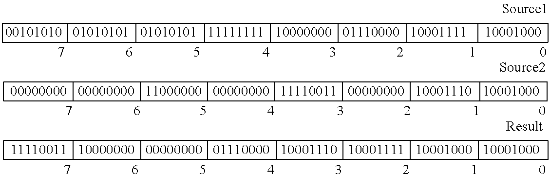 |
Table 7 illustrates the in-register representation of an unpack word operation.
| TABLE 7 |
 |
Table 8 illustrates the in-register representation of an unpack doubleword operation.
| TABLE 8 |
 |
In one embodiment of the present invention, to achieve efficient execution of the unpack operation parallelism is used. FIG. 10 illustrates one embodiment of a circuit that can perform an unpack operation on packed data.
The circuit of FIG. 10 includes the operation control circuit 800, a result register 1052, a result register 1053, and a result register 1054.
For example, in Table 9, an unpack word operation is performed. Operation control 800 will enable result register 1053 to output result[63:0] 860.
| TABLE 9 |
 |
However, if an unpack doubleword is performed, operation control 800 will enable result register 1054 to output result[63:0] 860. Table 10 illustrates this result.
| TABLE 10 |
 |
Therefore, the move, pack and unpack operations can manipulate multiple data elements. In prior art processors, to perform these types of manipulations, multiple separate operations would be needed to perform a single packed move, pack or unpack operation. The data lines for the packed data operations, in one embodiment, all carry relevant data. This leads to a higher performance computer system.
Claims (17)
1. An apparatus comprising:
a display device comprising graphics rendering devices;
a cache;
a decoder;
a register file operable to store a first packed data including a first plurality of data elements and a second packed data including a second plurality of data elements, wherein each data element in the first plurality of data elements corresponds to a different data element in the second plurality of data elements, in a respective position; and
a functional unit coupled to the display device, the cache, the decoder, and the register file, and operable to execute instructions specifying data manipulation operations, including:
a first move instruction that, when executed by the functional unit, causes data to be transferred from a first packed data register to a second packed data register;
a second move instruction that, when executed by the functional unit, causes data to be transferred between the first packed data register and a main memory; and
an unpack instruction that, when executed by the functional unit, causes only half of all data elements from the first plurality of data elements and corresponding data elements from the second plurality of data elements to be copied into the register file as a third plurality of data elements in a third packed data, wherein the third packed data is to include adjacent data elements from the first packed data.
2. The apparatus of claim 1 , wherein the decoder includes one or more sequencers.
3. The apparatus of claim 1 , wherein the first packed data register and the second packed data register are to hold 32 bits.
4. The apparatus of claim 1 , wherein the first packed data register and the second packed data register are to hold 64 bits.
5. The apparatus of claim 1 , wherein the apparatus is able to perform a packed data operation with saturation.
6. The apparatus of claim 1 , wherein the data elements from the first and second pluralities of data elements copied to the third packed data are not specified by the unpack instruction.
7. The apparatus of claim 1 , wherein the unpack instruction that, when executed by the functional unit, is to cause corresponding data elements from the first and second pluralities of data elements to be interleaved in the third packed data.
8. The apparatus of claim 7 , wherein the apparatus is able to perform a packed data operation with saturation.
9. The apparatus of claim 8 , wherein the data elements from the first and second pluralities of data elements to be copied into the third packed data are fixed for the unpack instruction.
10. A method comprising:
transferring data from a first packed data register to a second packed data register in response to a first move instruction;
transferring data from the first packed data register to main memory in response to a second move instruction;
storing a first packed data including a first plurality of data elements in a register file;
storing a second packed data including a second plurality of data elements in the register file;
decoding an unpack instruction;
in response to the decoder decoding the unpack instruction, copying only half of all data elements from the first plurality of data elements and corresponding data elements from the second plurality of data elements into the register file as a third plurality of data elements in a third packed data, wherein the third packed data is to include adjacent data elements from the first plurality of data elements.
11. The method claim 10 , wherein the decoder includes one or more sequencers.
12. The method of claim 10 , wherein the first packed data register and the second packed data register are to hold 32 bits.
13. The method of claim 10 , wherein packed data register and the second packed data register are to hold 64 bits.
14. A computer readable medium including code, that when executed, causes a machine to perform operations comprising:
transfer data from a first packed data register to a second packed data register in response to a first move instruction;
transfer data from the first packed data register to main memory in response to a second move instruction;
store a first packed data including a first plurality of data elements in a register file;
store a second packed data including a second plurality of data elements in the register file;
decode an unpack instruction;
in response to the decoder decoding the unpack instruction, copy only half of all data elements from the first plurality of data elements and corresponding data elements from the second plurality of data elements into the register file as a third plurality of data elements in a third packed data, wherein the third packed data is to include adjacent data elements from the first packed data.
15. The computer readable medium of claim 14 , wherein the decoder includes one or more sequencers.
16. The computer readable medium of claim 14 , wherein the first packed data register and the second packed data register are to hold 32 bits.
17. The computer readable medium of claim 14 , wherein the first packed data register and the second packed data register are to hold 64 bits.
Priority Applications (1)
| Application Number | Priority Date | Filing Date | Title |
|---|---|---|---|
| US13/730,837 US8793475B2 (en) | 1994-12-02 | 2012-12-29 | Method and apparatus for unpacking and moving packed data |
Applications Claiming Priority (6)
| Application Number | Priority Date | Filing Date | Title |
|---|---|---|---|
| US34904794A | 1994-12-02 | 1994-12-02 | |
| US08/791,003 US5802336A (en) | 1994-12-02 | 1997-01-27 | Microprocessor capable of unpacking packed data |
| US97443597A | 1997-11-20 | 1997-11-20 | |
| US65744700A | 2000-09-08 | 2000-09-08 | |
| US10/185,896 US8601246B2 (en) | 1994-12-02 | 2002-06-27 | Execution of instruction with element size control bit to interleavingly store half packed data elements of source registers in same size destination register |
| US13/730,837 US8793475B2 (en) | 1994-12-02 | 2012-12-29 | Method and apparatus for unpacking and moving packed data |
Related Parent Applications (1)
| Application Number | Title | Priority Date | Filing Date |
|---|---|---|---|
| US10/185,896 Continuation US8601246B2 (en) | 1994-12-02 | 2002-06-27 | Execution of instruction with element size control bit to interleavingly store half packed data elements of source registers in same size destination register |
Publications (2)
| Publication Number | Publication Date |
|---|---|
| US20130117547A1 US20130117547A1 (en) | 2013-05-09 |
| US8793475B2 true US8793475B2 (en) | 2014-07-29 |
Family
ID=23370692
Family Applications (21)
| Application Number | Title | Priority Date | Filing Date |
|---|---|---|---|
| US08/791,003 Expired - Lifetime US5802336A (en) | 1994-12-02 | 1997-01-27 | Microprocessor capable of unpacking packed data |
| US08/799,468 Expired - Lifetime US5881275A (en) | 1994-12-02 | 1997-02-13 | Method for unpacking a plurality of packed data into a result packed data |
| US08/974,435 Expired - Lifetime US6119216A (en) | 1994-12-02 | 1999-03-22 | Microprocessor capable of unpacking packed data in response to a unpack instruction |
| US09/657,448 Expired - Lifetime US6516406B1 (en) | 1994-12-02 | 2000-09-08 | Processor executing unpack instruction to interleave data elements from two packed data |
| US10/184,197 Abandoned US20030115441A1 (en) | 1994-12-02 | 2002-06-27 | Method and apparatus for packing data |
| US10/185,896 Expired - Fee Related US8601246B2 (en) | 1994-12-02 | 2002-06-27 | Execution of instruction with element size control bit to interleavingly store half packed data elements of source registers in same size destination register |
| US11/451,906 Expired - Fee Related US7966482B2 (en) | 1994-12-02 | 2006-06-12 | Interleaving saturated lower half of data elements from two source registers of packed data |
| US12/975,807 Expired - Fee Related US8521994B2 (en) | 1994-12-02 | 2010-12-22 | Interleaving corresponding data elements from part of two source registers to destination register in processor operable to perform saturation |
| US13/108,723 Expired - Fee Related US8190867B2 (en) | 1994-12-02 | 2011-05-16 | Packing two packed signed data in registers with saturation |
| US13/444,090 Expired - Fee Related US8495346B2 (en) | 1994-12-02 | 2012-04-11 | Processor executing pack and unpack instructions |
| US13/730,837 Expired - Fee Related US8793475B2 (en) | 1994-12-02 | 2012-12-29 | Method and apparatus for unpacking and moving packed data |
| US13/730,848 Expired - Fee Related US9015453B2 (en) | 1994-12-02 | 2012-12-29 | Packing odd bytes from two source registers of packed data |
| US13/730,841 Abandoned US20130124830A1 (en) | 1994-12-02 | 2012-12-29 | Method and Apparatus for Unpacking Packed Data |
| US13/730,832 Expired - Fee Related US9141387B2 (en) | 1994-12-02 | 2012-12-29 | Processor executing unpack and pack instructions specifying two source packed data operands and saturation |
| US13/730,849 Expired - Fee Related US8838946B2 (en) | 1994-12-02 | 2012-12-29 | Packing lower half bits of signed data elements in two source registers in a destination register with saturation |
| US13/730,839 Expired - Fee Related US9182983B2 (en) | 1994-12-02 | 2012-12-29 | Executing unpack instruction and pack instruction with saturation on packed data elements from two source operand registers |
| US13/730,831 Expired - Fee Related US8639914B2 (en) | 1994-12-02 | 2012-12-29 | Packing signed word elements from two source registers to saturated signed byte elements in destination register |
| US13/730,846 Expired - Fee Related US9389858B2 (en) | 1994-12-02 | 2012-12-29 | Orderly storing of corresponding packed bytes from first and second source registers in result register |
| US13/730,835 Expired - Fee Related US9223572B2 (en) | 1994-12-02 | 2012-12-29 | Interleaving half of packed data elements of size specified in instruction and stored in two source registers |
| US13/730,845 Expired - Fee Related US9361100B2 (en) | 1994-12-02 | 2012-12-29 | Packing saturated lower 8-bit elements from two source registers of packed 16-bit elements |
| US13/730,842 Expired - Fee Related US9116687B2 (en) | 1994-12-02 | 2012-12-29 | Packing in destination register half of each element with saturation from two source packed data registers |
Family Applications Before (10)
| Application Number | Title | Priority Date | Filing Date |
|---|---|---|---|
| US08/791,003 Expired - Lifetime US5802336A (en) | 1994-12-02 | 1997-01-27 | Microprocessor capable of unpacking packed data |
| US08/799,468 Expired - Lifetime US5881275A (en) | 1994-12-02 | 1997-02-13 | Method for unpacking a plurality of packed data into a result packed data |
| US08/974,435 Expired - Lifetime US6119216A (en) | 1994-12-02 | 1999-03-22 | Microprocessor capable of unpacking packed data in response to a unpack instruction |
| US09/657,448 Expired - Lifetime US6516406B1 (en) | 1994-12-02 | 2000-09-08 | Processor executing unpack instruction to interleave data elements from two packed data |
| US10/184,197 Abandoned US20030115441A1 (en) | 1994-12-02 | 2002-06-27 | Method and apparatus for packing data |
| US10/185,896 Expired - Fee Related US8601246B2 (en) | 1994-12-02 | 2002-06-27 | Execution of instruction with element size control bit to interleavingly store half packed data elements of source registers in same size destination register |
| US11/451,906 Expired - Fee Related US7966482B2 (en) | 1994-12-02 | 2006-06-12 | Interleaving saturated lower half of data elements from two source registers of packed data |
| US12/975,807 Expired - Fee Related US8521994B2 (en) | 1994-12-02 | 2010-12-22 | Interleaving corresponding data elements from part of two source registers to destination register in processor operable to perform saturation |
| US13/108,723 Expired - Fee Related US8190867B2 (en) | 1994-12-02 | 2011-05-16 | Packing two packed signed data in registers with saturation |
| US13/444,090 Expired - Fee Related US8495346B2 (en) | 1994-12-02 | 2012-04-11 | Processor executing pack and unpack instructions |
Family Applications After (10)
| Application Number | Title | Priority Date | Filing Date |
|---|---|---|---|
| US13/730,848 Expired - Fee Related US9015453B2 (en) | 1994-12-02 | 2012-12-29 | Packing odd bytes from two source registers of packed data |
| US13/730,841 Abandoned US20130124830A1 (en) | 1994-12-02 | 2012-12-29 | Method and Apparatus for Unpacking Packed Data |
| US13/730,832 Expired - Fee Related US9141387B2 (en) | 1994-12-02 | 2012-12-29 | Processor executing unpack and pack instructions specifying two source packed data operands and saturation |
| US13/730,849 Expired - Fee Related US8838946B2 (en) | 1994-12-02 | 2012-12-29 | Packing lower half bits of signed data elements in two source registers in a destination register with saturation |
| US13/730,839 Expired - Fee Related US9182983B2 (en) | 1994-12-02 | 2012-12-29 | Executing unpack instruction and pack instruction with saturation on packed data elements from two source operand registers |
| US13/730,831 Expired - Fee Related US8639914B2 (en) | 1994-12-02 | 2012-12-29 | Packing signed word elements from two source registers to saturated signed byte elements in destination register |
| US13/730,846 Expired - Fee Related US9389858B2 (en) | 1994-12-02 | 2012-12-29 | Orderly storing of corresponding packed bytes from first and second source registers in result register |
| US13/730,835 Expired - Fee Related US9223572B2 (en) | 1994-12-02 | 2012-12-29 | Interleaving half of packed data elements of size specified in instruction and stored in two source registers |
| US13/730,845 Expired - Fee Related US9361100B2 (en) | 1994-12-02 | 2012-12-29 | Packing saturated lower 8-bit elements from two source registers of packed 16-bit elements |
| US13/730,842 Expired - Fee Related US9116687B2 (en) | 1994-12-02 | 2012-12-29 | Packing in destination register half of each element with saturation from two source packed data registers |
Country Status (8)
| Country | Link |
|---|---|
| US (21) | US5802336A (en) |
| EP (2) | EP0795153A4 (en) |
| JP (1) | JP3615222B2 (en) |
| KR (1) | KR100329338B1 (en) |
| CN (5) | CN100412786C (en) |
| AU (1) | AU4464596A (en) |
| BR (1) | BR9509845A (en) |
| WO (1) | WO1996017291A1 (en) |
Cited By (1)
| Publication number | Priority date | Publication date | Assignee | Title |
|---|---|---|---|---|
| US10489158B2 (en) | 2014-09-26 | 2019-11-26 | Intel Corporation | Processors, methods, systems, and instructions to selectively fence only persistent storage of given data relative to subsequent stores |
Families Citing this family (80)
| Publication number | Priority date | Publication date | Assignee | Title |
|---|---|---|---|---|
| US5493687A (en) * | 1991-07-08 | 1996-02-20 | Seiko Epson Corporation | RISC microprocessor architecture implementing multiple typed register sets |
| US5539911A (en) * | 1991-07-08 | 1996-07-23 | Seiko Epson Corporation | High-performance, superscalar-based computer system with out-of-order instruction execution |
| DE69311330T2 (en) * | 1992-03-31 | 1997-09-25 | Seiko Epson Corp | COMMAND SEQUENCE PLANNING FROM A RISC SUPER SCALAR PROCESSOR |
| EP0638183B1 (en) * | 1992-05-01 | 1997-03-05 | Seiko Epson Corporation | A system and method for retiring instructions in a superscalar microprocessor |
| US5628021A (en) * | 1992-12-31 | 1997-05-06 | Seiko Epson Corporation | System and method for assigning tags to control instruction processing in a superscalar processor |
| KR100292300B1 (en) * | 1992-12-31 | 2001-09-17 | 야스카와 히데아키 | System and method for register renaming |
| KR100329338B1 (en) | 1994-12-02 | 2002-07-18 | 피터 엔. 데트킨 | Microprocessor with packing operation of composite operands |
| US6813699B1 (en) | 1995-06-02 | 2004-11-02 | Transmeta Corporation | Speculative address translation for processor using segmentation and optional paging |
| US7483935B2 (en) * | 1995-08-16 | 2009-01-27 | Microunity Systems Engineering, Inc. | System and method to implement a matrix multiply unit of a broadband processor |
| US7301541B2 (en) * | 1995-08-16 | 2007-11-27 | Microunity Systems Engineering, Inc. | Programmable processor and method with wide operations |
| US5953241A (en) * | 1995-08-16 | 1999-09-14 | Microunity Engeering Systems, Inc. | Multiplier array processing system with enhanced utilization at lower precision for group multiply and sum instruction |
| US6643765B1 (en) * | 1995-08-16 | 2003-11-04 | Microunity Systems Engineering, Inc. | Programmable processor with group floating point operations |
| US6295599B1 (en) | 1995-08-16 | 2001-09-25 | Microunity Systems Engineering | System and method for providing a wide operand architecture |
| US5742840A (en) | 1995-08-16 | 1998-04-21 | Microunity Systems Engineering, Inc. | General purpose, multiple precision parallel operation, programmable media processor |
| US7395298B2 (en) | 1995-08-31 | 2008-07-01 | Intel Corporation | Method and apparatus for performing multiply-add operations on packed data |
| US6385634B1 (en) * | 1995-08-31 | 2002-05-07 | Intel Corporation | Method for performing multiply-add operations on packed data |
| US6260137B1 (en) | 1997-09-12 | 2001-07-10 | Siemens Aktiengesellschaft | Data processing unit with digital signal processing capabilities |
| US6263420B1 (en) | 1997-09-17 | 2001-07-17 | Sony Corporation | Digital signal processor particularly suited for decoding digital audio |
| US6138274A (en) * | 1998-01-23 | 2000-10-24 | Lucent Technologies, Inc. | Method and apparatus for updating an online computer program |
| US6233671B1 (en) | 1998-03-31 | 2001-05-15 | Intel Corporation | Staggering execution of an instruction by dividing a full-width macro instruction into at least two partial-width micro instructions |
| US6122725A (en) * | 1998-03-31 | 2000-09-19 | Intel Corporation | Executing partial-width packed data instructions |
| US6230253B1 (en) * | 1998-03-31 | 2001-05-08 | Intel Corporation | Executing partial-width packed data instructions |
| US6041404A (en) | 1998-03-31 | 2000-03-21 | Intel Corporation | Dual function system and method for shuffling packed data elements |
| US6230257B1 (en) | 1998-03-31 | 2001-05-08 | Intel Corporation | Method and apparatus for staggering execution of a single packed data instruction using the same circuit |
| US6504550B1 (en) * | 1998-05-21 | 2003-01-07 | Mitsubishi Electric & Electronics Usa, Inc. | System for graphics processing employing semiconductor device |
| US6535218B1 (en) * | 1998-05-21 | 2003-03-18 | Mitsubishi Electric & Electronics Usa, Inc. | Frame buffer memory for graphic processing |
| US7932911B2 (en) * | 1998-08-24 | 2011-04-26 | Microunity Systems Engineering, Inc. | Processor for executing switch and translate instructions requiring wide operands |
| ATE557342T1 (en) | 1998-08-24 | 2012-05-15 | Microunity Systems Eng | PROCESSOR AND METHOD FOR MATRIX MULTIPLICATION WITH A WIDE OPERAND |
| US7242414B1 (en) * | 1999-07-30 | 2007-07-10 | Mips Technologies, Inc. | Processor having a compare extension of an instruction set architecture |
| US7346643B1 (en) * | 1999-07-30 | 2008-03-18 | Mips Technologies, Inc. | Processor with improved accuracy for multiply-add operations |
| US6446195B1 (en) * | 2000-01-31 | 2002-09-03 | Intel Corporation | Dyadic operations instruction processor with configurable functional blocks |
| US6829696B1 (en) * | 1999-12-30 | 2004-12-07 | Texas Instruments Incorporated | Data processing system with register store/load utilizing data packing/unpacking |
| US6638239B1 (en) * | 2000-04-14 | 2003-10-28 | Glaukos Corporation | Apparatus and method for treating glaucoma |
| GB0024312D0 (en) | 2000-10-04 | 2000-11-15 | Advanced Risc Mach Ltd | Single instruction multiple data processing |
| JP3779540B2 (en) | 2000-11-08 | 2006-05-31 | 株式会社ルネサステクノロジ | SIMD operation method that can specify multiple registers |
| FR2818145B1 (en) * | 2000-12-18 | 2003-11-28 | Oreal | ANTISOLAR COSMETIC COMPOSITIONS BASED ON A SYNERGETIC MIXTURE OF FILTERS AND USES |
| US7913261B2 (en) * | 2001-05-02 | 2011-03-22 | nCipher Corporation, Ltd. | Application-specific information-processing method, system, and apparatus |
| AU2002339867A1 (en) | 2001-09-04 | 2003-03-18 | Microunity Systems Engineering, Inc. | System and method for performing multiplication |
| US7430578B2 (en) | 2001-10-29 | 2008-09-30 | Intel Corporation | Method and apparatus for performing multiply-add operations on packed byte data |
| US7028171B2 (en) * | 2002-03-28 | 2006-04-11 | Intel Corporation | Multi-way select instructions using accumulated condition codes |
| US20030188135A1 (en) * | 2002-03-28 | 2003-10-02 | Intel Corporation | Addressing modes and/or instructions and/or operating modes for on-the-fly, precision adjustment of packed data |
| WO2004015563A1 (en) * | 2002-08-09 | 2004-02-19 | Intel Corporation | Multimedia coprocessor control mechanism including alignment or broadcast instructions |
| US6986023B2 (en) | 2002-08-09 | 2006-01-10 | Intel Corporation | Conditional execution of coprocessor instruction based on main processor arithmetic flags |
| US7392368B2 (en) * | 2002-08-09 | 2008-06-24 | Marvell International Ltd. | Cross multiply and add instruction and multiply and subtract instruction SIMD execution on real and imaginary components of a plurality of complex data elements |
| US7899855B2 (en) | 2003-09-08 | 2011-03-01 | Intel Corporation | Method, apparatus and instructions for parallel data conversions |
| EP1622009A1 (en) * | 2004-07-27 | 2006-02-01 | Texas Instruments Incorporated | JSM architecture and systems |
| US7457938B2 (en) * | 2005-09-30 | 2008-11-25 | Intel Corporation | Staggered execution stack for vector processing |
| WO2007085914A1 (en) * | 2006-01-27 | 2007-08-02 | Freescale Semiconductor, Inc. | Device and method for adding and subtracting two variables and a constant |
| US7958181B2 (en) | 2006-09-21 | 2011-06-07 | Intel Corporation | Method and apparatus for performing logical compare operations |
| US9069547B2 (en) * | 2006-09-22 | 2015-06-30 | Intel Corporation | Instruction and logic for processing text strings |
| US8341165B2 (en) | 2007-12-03 | 2012-12-25 | Intel Corporation | Method and apparatus for searching extensible markup language (XML) data |
| US8502819B1 (en) | 2007-12-17 | 2013-08-06 | Nvidia Corporation | System and method for performing ray tracing node traversal in image rendering |
| US8780128B2 (en) * | 2007-12-17 | 2014-07-15 | Nvidia Corporation | Contiguously packed data |
| US8289324B1 (en) | 2007-12-17 | 2012-10-16 | Nvidia Corporation | System, method, and computer program product for spatial hierarchy traversal |
| US8078836B2 (en) | 2007-12-30 | 2011-12-13 | Intel Corporation | Vector shuffle instructions operating on multiple lanes each having a plurality of data elements using a common set of per-lane control bits |
| US9086872B2 (en) * | 2009-06-30 | 2015-07-21 | Intel Corporation | Unpacking packed data in multiple lanes |
| US9747105B2 (en) * | 2009-12-17 | 2017-08-29 | Intel Corporation | Method and apparatus for performing a shift and exclusive or operation in a single instruction |
| US8555036B1 (en) | 2010-05-17 | 2013-10-08 | Nvidia Corporation | System and method for performing predicated selection of an output register |
| US8564589B1 (en) | 2010-05-17 | 2013-10-22 | Nvidia Corporation | System and method for accelerated ray-box intersection testing |
| US20120254589A1 (en) * | 2011-04-01 | 2012-10-04 | Jesus Corbal San Adrian | System, apparatus, and method for aligning registers |
| JP5853177B2 (en) * | 2011-04-08 | 2016-02-09 | パナソニックIpマネジメント株式会社 | Data processing apparatus and data processing method |
| CN104126170B (en) * | 2011-12-22 | 2018-05-18 | 英特尔公司 | Packaged data operation mask register arithmetic combining processor, method, system and instruction |
| CN104025039B (en) * | 2011-12-22 | 2018-05-08 | 英特尔公司 | Packaged data operation mask concatenation processor, method, system and instruction |
| US20140082333A1 (en) * | 2011-12-22 | 2014-03-20 | Elmoustapha Ould-Ahmed-Vall | Systems, apparatuses, and methods for performing an absolute difference calculation between corresponding packed data elements of two vector registers |
| US20130326196A1 (en) * | 2011-12-23 | 2013-12-05 | Elmoustapha Ould-Ahmed-Vall | Systems, apparatuses, and methods for performing vector packed unary decoding using masks |
| US8849885B2 (en) * | 2012-06-07 | 2014-09-30 | Via Technologies, Inc. | Saturation detector |
| US9436474B2 (en) | 2012-07-27 | 2016-09-06 | Microsoft Technology Licensing, Llc | Lock free streaming of executable code data |
| US9477467B2 (en) | 2013-03-30 | 2016-10-25 | Intel Corporation | Processors, methods, and systems to implement partial register accesses with masked full register accesses |
| WO2014203034A1 (en) * | 2013-06-18 | 2014-12-24 | Freescale Semiconductor, Inc. | Signal processing device and method of performing a pack-insert operation |
| US10228941B2 (en) * | 2013-06-28 | 2019-03-12 | Intel Corporation | Processors, methods, and systems to access a set of registers as either a plurality of smaller registers or a combined larger register |
| US9785565B2 (en) | 2014-06-30 | 2017-10-10 | Microunity Systems Engineering, Inc. | System and methods for expandably wide processor instructions |
| EP3001306A1 (en) * | 2014-09-25 | 2016-03-30 | Intel Corporation | Bit group interleave processors, methods, systems, and instructions |
| US9772848B2 (en) * | 2014-11-14 | 2017-09-26 | Intel Corporation | Three-dimensional morton coordinate conversion processors, methods, systems, and instructions |
| US9772849B2 (en) | 2014-11-14 | 2017-09-26 | Intel Corporation | Four-dimensional morton coordinate conversion processors, methods, systems, and instructions |
| US9772850B2 (en) | 2014-11-14 | 2017-09-26 | Intel Corporation | Morton coordinate adjustment processors, methods, systems, and instructions |
| US20170177351A1 (en) * | 2015-12-18 | 2017-06-22 | Intel Corporation | Instructions and Logic for Even and Odd Vector Get Operations |
| US11204764B2 (en) * | 2016-03-31 | 2021-12-21 | Intel Corporation | Processors, methods, systems, and instructions to Partition a source packed data into lanes |
| US10891131B2 (en) * | 2016-09-22 | 2021-01-12 | Intel Corporation | Processors, methods, systems, and instructions to consolidate data elements and generate index updates |
| US20180173527A1 (en) * | 2016-12-15 | 2018-06-21 | Optimum Semiconductor Technologies, Inc. | Floating point instruction format with embedded rounding rule |
| CN111381874B (en) * | 2018-12-28 | 2022-12-02 | 上海寒武纪信息科技有限公司 | COMPRESS instruction decoding method, data processing method, decoder and data processing device |
Citations (88)
| Publication number | Priority date | Publication date | Assignee | Title |
|---|---|---|---|---|
| US3541516A (en) | 1965-06-30 | 1970-11-17 | Ibm | Vector arithmetic multiprocessor computing system |
| US3711692A (en) | 1971-03-15 | 1973-01-16 | Goodyear Aerospace Corp | Determination of number of ones in a data field by addition |
| US3723715A (en) | 1971-08-25 | 1973-03-27 | Ibm | Fast modulo threshold operator binary adder for multi-number additions |
| GB1534230A (en) | 1976-11-11 | 1978-11-29 | Ibm | Data processing apparatus |
| US4139899A (en) | 1976-10-18 | 1979-02-13 | Burroughs Corporation | Shift network having a mask generator and a rotator |
| US4161784A (en) | 1978-01-05 | 1979-07-17 | Honeywell Information Systems, Inc. | Microprogrammable floating point arithmetic unit capable of performing arithmetic operations on long and short operands |
| US4229801A (en) | 1978-12-11 | 1980-10-21 | Data General Corporation | Floating point processor having concurrent exponent/mantissa operation |
| US4393468A (en) | 1981-03-26 | 1983-07-12 | Advanced Micro Devices, Inc. | Bit slice microprogrammable processor for signal processing applications |
| US4418383A (en) | 1980-06-30 | 1983-11-29 | International Business Machines Corporation | Data flow component for processor and microprocessor systems |
| US4481580A (en) | 1979-11-19 | 1984-11-06 | Sperry Corporation | Distributed data transfer control for parallel processor architectures |
| US4498177A (en) | 1982-08-30 | 1985-02-05 | Sperry Corporation | M Out of N code checker circuit |
| US4595911A (en) | 1983-07-14 | 1986-06-17 | Sperry Corporation | Programmable data reformat system |
| US4707800A (en) | 1985-03-04 | 1987-11-17 | Raytheon Company | Adder/substractor for variable length numbers |
| US4760525A (en) | 1986-06-10 | 1988-07-26 | The United States Of America As Represented By The Secretary Of The Air Force | Complex arithmetic vector processor for performing control function, scalar operation, and set-up of vector signal processing instruction |
| US4771379A (en) | 1985-10-23 | 1988-09-13 | Mitsubishi Denki Kabushiki Kaisha | Digital signal processor with parallel multipliers |
| US4825355A (en) | 1985-10-25 | 1989-04-25 | Hitachi, Ltd. | Instruction format for program control type data processing systems |
| US4868748A (en) | 1987-11-25 | 1989-09-19 | General Electric Company | Rapid processing of three-dimensional graphical objects from tomographic data |
| US4903228A (en) | 1988-11-09 | 1990-02-20 | International Business Machines Corporation | Single cycle merge/logic unit |
| EP0395348A2 (en) | 1989-04-28 | 1990-10-31 | Apple Computer, Inc. | Method and apparatus for multi-gauge computation |
| US4989168A (en) | 1987-11-30 | 1991-01-29 | Fujitsu Limited | Multiplying unit in a computer system, capable of population counting |
| US4992938A (en) | 1987-07-01 | 1991-02-12 | International Business Machines Corporation | Instruction control mechanism for a computing system with register renaming, map table and queues indicating available registers |
| US5008812A (en) | 1988-03-18 | 1991-04-16 | Digital Equipment Corporation | Context switching method and apparatus for use in a vector processing system |
| EP0463975A2 (en) | 1990-06-29 | 1992-01-02 | Digital Equipment Corporation | Byte-compare operation for high-performance processor |
| US5081698A (en) | 1989-02-14 | 1992-01-14 | Intel Corporation | Method and apparatus for graphics display data manipulation |
| US5091848A (en) | 1987-04-10 | 1992-02-25 | Hitachi, Ltd. | Vector processor for merging vector elements in ascending order merging operation or descending order merging operation |
| US5095457A (en) | 1989-02-02 | 1992-03-10 | Samsung Electronics Co., Ltd. | Digital multiplier employing CMOS transistors |
| WO1992008188A1 (en) | 1990-11-02 | 1992-05-14 | Seiko Epson Corporation | Semiconductor device |
| EP0485776A2 (en) | 1990-11-15 | 1992-05-20 | Motorola, Inc. | A method for executing graphics pixel packing instructions in a data processor |
| US5127098A (en) | 1989-04-12 | 1992-06-30 | Sun Microsystems, Inc. | Method and apparatus for the context switching of devices |
| US5168571A (en) | 1990-01-24 | 1992-12-01 | International Business Machines Corporation | System for aligning bytes of variable multi-bytes length operand based on alu byte length and a number of unprocessed byte data |
| WO1993001543A1 (en) | 1991-07-08 | 1993-01-21 | S-Mos Systems, Inc. | Risc microprocessor architecture implementing multiple typed register sets |
| US5187679A (en) | 1991-06-05 | 1993-02-16 | International Business Machines Corporation | Generalized 7/3 counters |
| US5193159A (en) | 1986-09-24 | 1993-03-09 | Hitachi, Ltd. | Microprocessor system |
| US5212777A (en) | 1989-11-17 | 1993-05-18 | Texas Instruments Incorporated | Multi-processor reconfigurable in single instruction multiple data (SIMD) and multiple instruction multiple data (MIMD) modes and method of operation |
| US5241635A (en) | 1988-11-18 | 1993-08-31 | Massachusetts Institute Of Technology | Tagged token data processing system with operand matching in activation frames |
| US5265204A (en) | 1984-10-05 | 1993-11-23 | Hitachi, Ltd. | Method and apparatus for bit operational process |
| US5267350A (en) | 1989-10-26 | 1993-11-30 | Kenji Matsubara | Method for fetching plural instructions using single fetch request in accordance with empty state of instruction buffers and setting of flag latches |
| US5268854A (en) | 1990-11-13 | 1993-12-07 | Kabushiki Kaisha Toshiba | Microprocessor with a function for three-dimensional graphic processing |
| US5268995A (en) | 1990-11-21 | 1993-12-07 | Motorola, Inc. | Method for executing graphics Z-compare and pixel merge instructions in a data processor |
| US5276891A (en) | 1990-01-11 | 1994-01-04 | Bull Hn Information Systems Inc. | Alignment of sign, data, edit byte operand results for storage in memory |
| US5327543A (en) | 1987-09-10 | 1994-07-05 | Hitachi Ltd | System for selectively masking operand portions for processing thereof |
| EP0605868A1 (en) | 1993-01-08 | 1994-07-13 | International Business Machines Corporation | Method and system for indexing the assignment of intermediate storage buffers in a superscalar processor system |
| US5390135A (en) | 1993-11-29 | 1995-02-14 | Hewlett-Packard | Parallel shift and add circuit and method |
| US5408670A (en) | 1992-12-18 | 1995-04-18 | Xerox Corporation | Performing arithmetic in parallel on composite operands with packed multi-bit components |
| US5423010A (en) | 1992-01-24 | 1995-06-06 | C-Cube Microsystems | Structure and method for packing and unpacking a stream of N-bit data to and from a stream of N-bit data words |
| US5426783A (en) | 1992-11-02 | 1995-06-20 | Amdahl Corporation | System for processing eight bytes or less by the move, pack and unpack instruction of the ESA/390 instruction set |
| US5465374A (en) | 1993-01-12 | 1995-11-07 | International Business Machines Corporation | Processor for processing data string by byte-by-byte |
| US5467473A (en) | 1993-01-08 | 1995-11-14 | International Business Machines Corporation | Out of order instruction load and store comparison |
| US5481719A (en) | 1994-09-09 | 1996-01-02 | International Business Machines Corporation | Exception handling method and apparatus for a microkernel data processing system |
| US5487159A (en) | 1993-12-23 | 1996-01-23 | Unisys Corporation | System for processing shift, mask, and merge operations in one instruction |
| US5499352A (en) | 1993-09-30 | 1996-03-12 | Intel Corporation | Floating point register alias table FXCH and retirement floating point register array |
| US5499376A (en) | 1993-12-06 | 1996-03-12 | Cpu Technology, Inc. | High speed mask and logical combination operations for parallel processor units |
| US5507000A (en) | 1994-09-26 | 1996-04-09 | Bull Hn Information Systems Inc. | Sharing of register stack by two execution units in a central processor |
| US5519841A (en) | 1992-11-12 | 1996-05-21 | Digital Equipment Corporation | Multi instruction register mapper |
| US5522051A (en) | 1992-07-29 | 1996-05-28 | Intel Corporation | Method and apparatus for stack manipulation in a pipelined processor |
| US5535397A (en) | 1993-06-30 | 1996-07-09 | Intel Corporation | Method and apparatus for providing a context switch in response to an interrupt in a computer process |
| US5537606A (en) | 1995-01-31 | 1996-07-16 | International Business Machines Corporation | Scalar pipeline replication for parallel vector element processing |
| US5541865A (en) | 1993-12-30 | 1996-07-30 | Intel Corporation | Method and apparatus for performing a population count operation |
| US5546554A (en) | 1994-02-02 | 1996-08-13 | Sun Microsystems, Inc. | Apparatus for dynamic register management in a floating point unit |
| US5590350A (en) | 1993-11-30 | 1996-12-31 | Texas Instruments Incorporated | Three input arithmetic logic unit with mask generator |
| US5594437A (en) | 1994-08-01 | 1997-01-14 | Motorola, Inc. | Circuit and method of unpacking a serial bitstream |
| US5625374A (en) | 1993-09-07 | 1997-04-29 | Apple Computer, Inc. | Method for parallel interpolation of images |
| US5634118A (en) | 1995-04-10 | 1997-05-27 | Exponential Technology, Inc. | Splitting a floating-point stack-exchange instruction for merging into surrounding instructions by operand translation |
| US5649225A (en) | 1994-06-01 | 1997-07-15 | Advanced Micro Devices, Inc. | Resynchronization of a superscalar processor |
| US5651125A (en) | 1993-10-29 | 1997-07-22 | Advanced Micro Devices, Inc. | High performance superscalar microprocessor including a common reorder buffer and common register file for both integer and floating point operations |
| US5657253A (en) | 1992-05-15 | 1997-08-12 | Intel Corporation | Apparatus for monitoring the performance of a microprocessor |
| US5669012A (en) | 1993-05-21 | 1997-09-16 | Mitsubishi Denki Kabushiki Kaisha | Data processor and control circuit for inserting/extracting data to/from an optional byte position of a register |
| US5675777A (en) | 1990-01-29 | 1997-10-07 | Hipercore, Inc. | Architecture for minimal instruction set computing system |
| US5675526A (en) | 1994-12-01 | 1997-10-07 | Intel Corporation | Processor performing packed data multiplication |
| US5680161A (en) | 1991-04-03 | 1997-10-21 | Radius Inc. | Method and apparatus for high speed graphics data compression |
| US5687336A (en) | 1996-01-11 | 1997-11-11 | Exponential Technology, Inc. | Stack push/pop tracking and pairing in a pipelined processor |
| US5696955A (en) | 1994-06-01 | 1997-12-09 | Advanced Micro Devices, Inc. | Floating point stack and exchange instruction |
| US5701508A (en) | 1995-12-19 | 1997-12-23 | Intel Corporation | Executing different instructions that cause different data type operations to be performed on single logical register file |
| US5721892A (en) | 1995-08-31 | 1998-02-24 | Intel Corporation | Method and apparatus for performing multiply-subtract operations on packed data |
| US5734874A (en) | 1994-04-29 | 1998-03-31 | Sun Microsystems, Inc. | Central processing unit with integrated graphics functions |
| US5752001A (en) | 1995-06-01 | 1998-05-12 | Intel Corporation | Method and apparatus employing Viterbi scoring using SIMD instructions for data recognition |
| US5760792A (en) | 1995-05-01 | 1998-06-02 | Intergraph Corporation | Fifo logical addresses for control and error recovery |
| US5781457A (en) | 1994-03-08 | 1998-07-14 | Exponential Technology, Inc. | Merge/mask, rotate/shift, and boolean operations from two instruction sets executed in a vectored mux on a dual-ALU |
| US5802336A (en) | 1994-12-02 | 1998-09-01 | Intel Corporation | Microprocessor capable of unpacking packed data |
| US5819101A (en) | 1994-12-02 | 1998-10-06 | Intel Corporation | Method for packing a plurality of packed data elements in response to a pack instruction |
| US5835748A (en) | 1995-12-19 | 1998-11-10 | Intel Corporation | Method for executing different sets of instructions that cause a processor to perform different data type operations on different physical registers files that logically appear to software as a single aliased register file |
| US5835782A (en) | 1996-03-04 | 1998-11-10 | Intel Corporation | Packed/add and packed subtract operations |
| US5852726A (en) | 1995-12-19 | 1998-12-22 | Intel Corporation | Method and apparatus for executing two types of instructions that specify registers of a shared logical register file in a stack and a non-stack referenced manner |
| US5857096A (en) | 1995-12-19 | 1999-01-05 | Intel Corporation | Microarchitecture for implementing an instruction to clear the tags of a stack reference register file |
| US5862067A (en) | 1995-12-29 | 1999-01-19 | Intel Corporation | Method and apparatus for providing high numerical accuracy with packed multiply-add or multiply-subtract operations |
| US5909552A (en) | 1990-11-15 | 1999-06-01 | International Business Machines Corporation | Method and apparatus for processing packed data |
| US5940859A (en) | 1995-12-19 | 1999-08-17 | Intel Corporation | Emptying packed data state during execution of packed data instructions |
| US6115812A (en) | 1998-04-01 | 2000-09-05 | Intel Corporation | Method and apparatus for efficient vertical SIMD computations |
Family Cites Families (6)
| Publication number | Priority date | Publication date | Assignee | Title |
|---|---|---|---|---|
| JPS5537648A (en) * | 1978-09-07 | 1980-03-15 | Matsushita Electric Ind Co Ltd | Instruction decoder circuit |
| US5168751A (en) * | 1991-08-01 | 1992-12-08 | Raymond Hwang | Digital tire pressure gauge |
| US5239399A (en) | 1991-08-22 | 1993-08-24 | Radiant Technologies | Electrical-optical interface device |
| US5530835A (en) | 1991-09-18 | 1996-06-25 | Ncr Corporation | Computer memory data merging technique for computers with write-back caches |
| KR950009687B1 (en) * | 1992-06-30 | 1995-08-26 | 삼성항공산업주식회사 | High speed ladder instruction processing apparatus for programnable logic controller |
| US5717947A (en) * | 1993-03-31 | 1998-02-10 | Motorola, Inc. | Data processing system and method thereof |
-
1995
- 1995-12-01 KR KR1019970703682A patent/KR100329338B1/en not_active IP Right Cessation
- 1995-12-01 CN CNB02126161XA patent/CN100412786C/en not_active Expired - Lifetime
- 1995-12-01 EP EP95943362A patent/EP0795153A4/en not_active Withdrawn
- 1995-12-01 AU AU44645/96A patent/AU4464596A/en not_active Abandoned
- 1995-12-01 CN CNB021261601A patent/CN1326033C/en not_active Expired - Lifetime
- 1995-12-01 CN CN95197430A patent/CN1094610C/en not_active Expired - Lifetime
- 1995-12-01 CN CN201210161092.2A patent/CN102841776B/en not_active Expired - Lifetime
- 1995-12-01 WO PCT/US1995/015713 patent/WO1996017291A1/en active IP Right Grant
- 1995-12-01 EP EP20020078326 patent/EP1265132A3/en not_active Withdrawn
- 1995-12-01 BR BR9509845A patent/BR9509845A/en not_active IP Right Cessation
- 1995-12-01 JP JP51912596A patent/JP3615222B2/en not_active Expired - Lifetime
- 1995-12-01 CN CN2007101657203A patent/CN101211255B/en not_active Expired - Lifetime
-
1997
- 1997-01-27 US US08/791,003 patent/US5802336A/en not_active Expired - Lifetime
- 1997-02-13 US US08/799,468 patent/US5881275A/en not_active Expired - Lifetime
-
1999
- 1999-03-22 US US08/974,435 patent/US6119216A/en not_active Expired - Lifetime
-
2000
- 2000-09-08 US US09/657,448 patent/US6516406B1/en not_active Expired - Lifetime
-
2002
- 2002-06-27 US US10/184,197 patent/US20030115441A1/en not_active Abandoned
- 2002-06-27 US US10/185,896 patent/US8601246B2/en not_active Expired - Fee Related
-
2006
- 2006-06-12 US US11/451,906 patent/US7966482B2/en not_active Expired - Fee Related
-
2010
- 2010-12-22 US US12/975,807 patent/US8521994B2/en not_active Expired - Fee Related
-
2011
- 2011-05-16 US US13/108,723 patent/US8190867B2/en not_active Expired - Fee Related
-
2012
- 2012-04-11 US US13/444,090 patent/US8495346B2/en not_active Expired - Fee Related
- 2012-12-29 US US13/730,837 patent/US8793475B2/en not_active Expired - Fee Related
- 2012-12-29 US US13/730,848 patent/US9015453B2/en not_active Expired - Fee Related
- 2012-12-29 US US13/730,841 patent/US20130124830A1/en not_active Abandoned
- 2012-12-29 US US13/730,832 patent/US9141387B2/en not_active Expired - Fee Related
- 2012-12-29 US US13/730,849 patent/US8838946B2/en not_active Expired - Fee Related
- 2012-12-29 US US13/730,839 patent/US9182983B2/en not_active Expired - Fee Related
- 2012-12-29 US US13/730,831 patent/US8639914B2/en not_active Expired - Fee Related
- 2012-12-29 US US13/730,846 patent/US9389858B2/en not_active Expired - Fee Related
- 2012-12-29 US US13/730,835 patent/US9223572B2/en not_active Expired - Fee Related
- 2012-12-29 US US13/730,845 patent/US9361100B2/en not_active Expired - Fee Related
- 2012-12-29 US US13/730,842 patent/US9116687B2/en not_active Expired - Fee Related
Patent Citations (95)
| Publication number | Priority date | Publication date | Assignee | Title |
|---|---|---|---|---|
| US3541516A (en) | 1965-06-30 | 1970-11-17 | Ibm | Vector arithmetic multiprocessor computing system |
| US3711692A (en) | 1971-03-15 | 1973-01-16 | Goodyear Aerospace Corp | Determination of number of ones in a data field by addition |
| US3723715A (en) | 1971-08-25 | 1973-03-27 | Ibm | Fast modulo threshold operator binary adder for multi-number additions |
| US4139899A (en) | 1976-10-18 | 1979-02-13 | Burroughs Corporation | Shift network having a mask generator and a rotator |
| GB1534230A (en) | 1976-11-11 | 1978-11-29 | Ibm | Data processing apparatus |
| US4141005A (en) | 1976-11-11 | 1979-02-20 | International Business Machines Corporation | Data format converting apparatus for use in a digital data processor |
| US4161784A (en) | 1978-01-05 | 1979-07-17 | Honeywell Information Systems, Inc. | Microprogrammable floating point arithmetic unit capable of performing arithmetic operations on long and short operands |
| US4229801A (en) | 1978-12-11 | 1980-10-21 | Data General Corporation | Floating point processor having concurrent exponent/mantissa operation |
| US4481580A (en) | 1979-11-19 | 1984-11-06 | Sperry Corporation | Distributed data transfer control for parallel processor architectures |
| US4418383A (en) | 1980-06-30 | 1983-11-29 | International Business Machines Corporation | Data flow component for processor and microprocessor systems |
| US4393468A (en) | 1981-03-26 | 1983-07-12 | Advanced Micro Devices, Inc. | Bit slice microprogrammable processor for signal processing applications |
| US4498177A (en) | 1982-08-30 | 1985-02-05 | Sperry Corporation | M Out of N code checker circuit |
| US4595911A (en) | 1983-07-14 | 1986-06-17 | Sperry Corporation | Programmable data reformat system |
| US5265204A (en) | 1984-10-05 | 1993-11-23 | Hitachi, Ltd. | Method and apparatus for bit operational process |
| US4707800A (en) | 1985-03-04 | 1987-11-17 | Raytheon Company | Adder/substractor for variable length numbers |
| US4771379A (en) | 1985-10-23 | 1988-09-13 | Mitsubishi Denki Kabushiki Kaisha | Digital signal processor with parallel multipliers |
| US4825355A (en) | 1985-10-25 | 1989-04-25 | Hitachi, Ltd. | Instruction format for program control type data processing systems |
| US4760525A (en) | 1986-06-10 | 1988-07-26 | The United States Of America As Represented By The Secretary Of The Air Force | Complex arithmetic vector processor for performing control function, scalar operation, and set-up of vector signal processing instruction |
| US5193159A (en) | 1986-09-24 | 1993-03-09 | Hitachi, Ltd. | Microprocessor system |
| US5091848A (en) | 1987-04-10 | 1992-02-25 | Hitachi, Ltd. | Vector processor for merging vector elements in ascending order merging operation or descending order merging operation |
| US4992938A (en) | 1987-07-01 | 1991-02-12 | International Business Machines Corporation | Instruction control mechanism for a computing system with register renaming, map table and queues indicating available registers |
| US5327543A (en) | 1987-09-10 | 1994-07-05 | Hitachi Ltd | System for selectively masking operand portions for processing thereof |
| US4868748A (en) | 1987-11-25 | 1989-09-19 | General Electric Company | Rapid processing of three-dimensional graphical objects from tomographic data |
| US4989168A (en) | 1987-11-30 | 1991-01-29 | Fujitsu Limited | Multiplying unit in a computer system, capable of population counting |
| US5008812A (en) | 1988-03-18 | 1991-04-16 | Digital Equipment Corporation | Context switching method and apparatus for use in a vector processing system |
| US4903228A (en) | 1988-11-09 | 1990-02-20 | International Business Machines Corporation | Single cycle merge/logic unit |
| US5241635A (en) | 1988-11-18 | 1993-08-31 | Massachusetts Institute Of Technology | Tagged token data processing system with operand matching in activation frames |
| US5095457A (en) | 1989-02-02 | 1992-03-10 | Samsung Electronics Co., Ltd. | Digital multiplier employing CMOS transistors |
| US5081698A (en) | 1989-02-14 | 1992-01-14 | Intel Corporation | Method and apparatus for graphics display data manipulation |
| US5127098A (en) | 1989-04-12 | 1992-06-30 | Sun Microsystems, Inc. | Method and apparatus for the context switching of devices |
| EP0395348A2 (en) | 1989-04-28 | 1990-10-31 | Apple Computer, Inc. | Method and apparatus for multi-gauge computation |
| US5267350A (en) | 1989-10-26 | 1993-11-30 | Kenji Matsubara | Method for fetching plural instructions using single fetch request in accordance with empty state of instruction buffers and setting of flag latches |
| US5212777A (en) | 1989-11-17 | 1993-05-18 | Texas Instruments Incorporated | Multi-processor reconfigurable in single instruction multiple data (SIMD) and multiple instruction multiple data (MIMD) modes and method of operation |
| US5276891A (en) | 1990-01-11 | 1994-01-04 | Bull Hn Information Systems Inc. | Alignment of sign, data, edit byte operand results for storage in memory |
| US5168571A (en) | 1990-01-24 | 1992-12-01 | International Business Machines Corporation | System for aligning bytes of variable multi-bytes length operand based on alu byte length and a number of unprocessed byte data |
| US5675777A (en) | 1990-01-29 | 1997-10-07 | Hipercore, Inc. | Architecture for minimal instruction set computing system |
| EP0463975A2 (en) | 1990-06-29 | 1992-01-02 | Digital Equipment Corporation | Byte-compare operation for high-performance processor |
| WO1992008188A1 (en) | 1990-11-02 | 1992-05-14 | Seiko Epson Corporation | Semiconductor device |
| US5268854A (en) | 1990-11-13 | 1993-12-07 | Kabushiki Kaisha Toshiba | Microprocessor with a function for three-dimensional graphic processing |
| EP0485776A2 (en) | 1990-11-15 | 1992-05-20 | Motorola, Inc. | A method for executing graphics pixel packing instructions in a data processor |
| US5909552A (en) | 1990-11-15 | 1999-06-01 | International Business Machines Corporation | Method and apparatus for processing packed data |
| US5268995A (en) | 1990-11-21 | 1993-12-07 | Motorola, Inc. | Method for executing graphics Z-compare and pixel merge instructions in a data processor |
| US5680161A (en) | 1991-04-03 | 1997-10-21 | Radius Inc. | Method and apparatus for high speed graphics data compression |
| US5187679A (en) | 1991-06-05 | 1993-02-16 | International Business Machines Corporation | Generalized 7/3 counters |
| WO1993001543A1 (en) | 1991-07-08 | 1993-01-21 | S-Mos Systems, Inc. | Risc microprocessor architecture implementing multiple typed register sets |
| US5560035A (en) | 1991-07-08 | 1996-09-24 | Seiko Epson Corporation | RISC microprocessor architecture implementing multiple typed register sets |
| US5423010A (en) | 1992-01-24 | 1995-06-06 | C-Cube Microsystems | Structure and method for packing and unpacking a stream of N-bit data to and from a stream of N-bit data words |
| US5657253A (en) | 1992-05-15 | 1997-08-12 | Intel Corporation | Apparatus for monitoring the performance of a microprocessor |
| US5522051A (en) | 1992-07-29 | 1996-05-28 | Intel Corporation | Method and apparatus for stack manipulation in a pipelined processor |
| US5426783A (en) | 1992-11-02 | 1995-06-20 | Amdahl Corporation | System for processing eight bytes or less by the move, pack and unpack instruction of the ESA/390 instruction set |
| US5519841A (en) | 1992-11-12 | 1996-05-21 | Digital Equipment Corporation | Multi instruction register mapper |
| US5408670A (en) | 1992-12-18 | 1995-04-18 | Xerox Corporation | Performing arithmetic in parallel on composite operands with packed multi-bit components |
| EP0605868A1 (en) | 1993-01-08 | 1994-07-13 | International Business Machines Corporation | Method and system for indexing the assignment of intermediate storage buffers in a superscalar processor system |
| US5467473A (en) | 1993-01-08 | 1995-11-14 | International Business Machines Corporation | Out of order instruction load and store comparison |
| US5465374A (en) | 1993-01-12 | 1995-11-07 | International Business Machines Corporation | Processor for processing data string by byte-by-byte |
| US5669012A (en) | 1993-05-21 | 1997-09-16 | Mitsubishi Denki Kabushiki Kaisha | Data processor and control circuit for inserting/extracting data to/from an optional byte position of a register |
| US5535397A (en) | 1993-06-30 | 1996-07-09 | Intel Corporation | Method and apparatus for providing a context switch in response to an interrupt in a computer process |
| US5625374A (en) | 1993-09-07 | 1997-04-29 | Apple Computer, Inc. | Method for parallel interpolation of images |
| US5499352A (en) | 1993-09-30 | 1996-03-12 | Intel Corporation | Floating point register alias table FXCH and retirement floating point register array |
| US5651125A (en) | 1993-10-29 | 1997-07-22 | Advanced Micro Devices, Inc. | High performance superscalar microprocessor including a common reorder buffer and common register file for both integer and floating point operations |
| US5390135A (en) | 1993-11-29 | 1995-02-14 | Hewlett-Packard | Parallel shift and add circuit and method |
| US5590350A (en) | 1993-11-30 | 1996-12-31 | Texas Instruments Incorporated | Three input arithmetic logic unit with mask generator |
| US5499376A (en) | 1993-12-06 | 1996-03-12 | Cpu Technology, Inc. | High speed mask and logical combination operations for parallel processor units |
| US5487159A (en) | 1993-12-23 | 1996-01-23 | Unisys Corporation | System for processing shift, mask, and merge operations in one instruction |
| US5541865A (en) | 1993-12-30 | 1996-07-30 | Intel Corporation | Method and apparatus for performing a population count operation |
| US5546554A (en) | 1994-02-02 | 1996-08-13 | Sun Microsystems, Inc. | Apparatus for dynamic register management in a floating point unit |
| US5781457A (en) | 1994-03-08 | 1998-07-14 | Exponential Technology, Inc. | Merge/mask, rotate/shift, and boolean operations from two instruction sets executed in a vectored mux on a dual-ALU |
| US5734874A (en) | 1994-04-29 | 1998-03-31 | Sun Microsystems, Inc. | Central processing unit with integrated graphics functions |
| US5938756A (en) | 1994-04-29 | 1999-08-17 | Sun Microsystems, Inc. | Central processing unit with integrated graphics functions |
| US5649225A (en) | 1994-06-01 | 1997-07-15 | Advanced Micro Devices, Inc. | Resynchronization of a superscalar processor |
| US5696955A (en) | 1994-06-01 | 1997-12-09 | Advanced Micro Devices, Inc. | Floating point stack and exchange instruction |
| US5594437A (en) | 1994-08-01 | 1997-01-14 | Motorola, Inc. | Circuit and method of unpacking a serial bitstream |
| US5481719A (en) | 1994-09-09 | 1996-01-02 | International Business Machines Corporation | Exception handling method and apparatus for a microkernel data processing system |
| US5507000A (en) | 1994-09-26 | 1996-04-09 | Bull Hn Information Systems Inc. | Sharing of register stack by two execution units in a central processor |
| US5677862A (en) | 1994-12-01 | 1997-10-14 | Intel Corporation | Method for multiplying packed data |
| US5675526A (en) | 1994-12-01 | 1997-10-07 | Intel Corporation | Processor performing packed data multiplication |
| US5881275A (en) | 1994-12-02 | 1999-03-09 | Intel Corporation | Method for unpacking a plurality of packed data into a result packed data |
| US6119216A (en) | 1994-12-02 | 2000-09-12 | Intel Corporation | Microprocessor capable of unpacking packed data in response to a unpack instruction |
| US6516406B1 (en) | 1994-12-02 | 2003-02-04 | Intel Corporation | Processor executing unpack instruction to interleave data elements from two packed data |
| US5802336A (en) | 1994-12-02 | 1998-09-01 | Intel Corporation | Microprocessor capable of unpacking packed data |
| US5819101A (en) | 1994-12-02 | 1998-10-06 | Intel Corporation | Method for packing a plurality of packed data elements in response to a pack instruction |
| US5537606A (en) | 1995-01-31 | 1996-07-16 | International Business Machines Corporation | Scalar pipeline replication for parallel vector element processing |
| US5634118A (en) | 1995-04-10 | 1997-05-27 | Exponential Technology, Inc. | Splitting a floating-point stack-exchange instruction for merging into surrounding instructions by operand translation |
| US5760792A (en) | 1995-05-01 | 1998-06-02 | Intergraph Corporation | Fifo logical addresses for control and error recovery |
| US5752001A (en) | 1995-06-01 | 1998-05-12 | Intel Corporation | Method and apparatus employing Viterbi scoring using SIMD instructions for data recognition |
| US5721892A (en) | 1995-08-31 | 1998-02-24 | Intel Corporation | Method and apparatus for performing multiply-subtract operations on packed data |
| US5852726A (en) | 1995-12-19 | 1998-12-22 | Intel Corporation | Method and apparatus for executing two types of instructions that specify registers of a shared logical register file in a stack and a non-stack referenced manner |
| US5857096A (en) | 1995-12-19 | 1999-01-05 | Intel Corporation | Microarchitecture for implementing an instruction to clear the tags of a stack reference register file |
| US5835748A (en) | 1995-12-19 | 1998-11-10 | Intel Corporation | Method for executing different sets of instructions that cause a processor to perform different data type operations on different physical registers files that logically appear to software as a single aliased register file |
| US5940859A (en) | 1995-12-19 | 1999-08-17 | Intel Corporation | Emptying packed data state during execution of packed data instructions |
| US5701508A (en) | 1995-12-19 | 1997-12-23 | Intel Corporation | Executing different instructions that cause different data type operations to be performed on single logical register file |
| US5862067A (en) | 1995-12-29 | 1999-01-19 | Intel Corporation | Method and apparatus for providing high numerical accuracy with packed multiply-add or multiply-subtract operations |
| US5687336A (en) | 1996-01-11 | 1997-11-11 | Exponential Technology, Inc. | Stack push/pop tracking and pairing in a pipelined processor |
| US5835782A (en) | 1996-03-04 | 1998-11-10 | Intel Corporation | Packed/add and packed subtract operations |
| US6115812A (en) | 1998-04-01 | 2000-09-05 | Intel Corporation | Method and apparatus for efficient vertical SIMD computations |
Non-Patent Citations (56)
| Title |
|---|
| "Complaint" In the United States District Court for the District of Delaware, In the matter of Transmeta v. Intel Corporation, (Oct. 11, 2006), 1-7. |
| "Final Joint Claim Construction Chart", In the United States District Court for the District of Delaware, In the Matter of Transmeta Corporation v. Intel Corporation, C.A. No. 06-633 (GMS), (Oct. 10, 2007), pp. 1-215. |
| "First Amended Complaint", In the United States District Court for the District of Delaware, In the Matter of Transmeta Corporation v. Intel CorporationC.A. No. 06-663 (GMS), (Dec. 12, 2006), 1-8. |
| "Intel Corporation'S Answer, Affirmative Defenses, and Counterclaims to Transmeta'S First Amended Complaint", In the United States District Court for the District of Delaware, In the matter of Transmeta Corporation v. Intel Corporation, Civil Action No. 06-663-GMS, (Jan. 9, 2007), 1-27. |
| "Intel Corporation's Opening Claim Construction Brief", In the United States District Court for the District of Delaware, In the Matter of Transmeta Corporation v. Intel Corporation, C.A. No. 06-633-GMS, (Oct. 19, 2007), pp. 1-76. |
| "Intel Corporation's Responses to Transmeta's First Set of Interrogatories to Intel Corporation (Nos. 1-24)", In the United States District Court for the District of Delaware, In the Matter of Transmeta Corporation v. Intel Corporation, C.A. No. 06-633-GMS, (May 18, 2007), pp. 1-132. |
| "Intel Corporation's Supplemental Responses to Transmeta Interrogatory Nos. 8, 9, 12, 19 and 21-23", In the United States District Court for the District of Delaware, In the Matter of Transmeta Corporation v. Intel Corporation, C.A. No. 06-633-GMS, (Aug. 23, 2007), pp. 1-27. |
| "Transmeta Corporation's Amended and Supplemental Responses to Intel Corporation's First Set of Interrogatories (Nos. 1, 3, 4, 5, 8, 13, 15)" (Redacted Version), In the United States District Court for the District of Delaware, In the Matter of Transmeta Corporation v. Intel Corporation, C.A. No. 06-633-GMS, (Aug. 23, 2007), 84 pages (including Exhibits 15-18 totaling 46 pages). |
| "Transmeta Corporation's Opening Claim Construction Brief", In the United States District Court for the District of Delaware, In the Matter of Transmeta v. Intel Corporation, C.A. No. 06-633-GMS, (Oct. 19, 2007), pp. 1-66. |
| "Transmeta Corporation'S Reply to Intel Corporation'S Counterclaims to the First Amended Complaint", In the United States District Court for the District of Delaware, In the matter of Transmeta v. Intel Corporation, (Feb. 28, 2007), 1-20. |
| "Transmeta Corporation'S Responses to Intel Corporation's First Set of Interrogatories (Nos. 1-20)", In the United States District Court for the District fo Delaware, In the matter of Transmeta Corporation v. Intel Corporation, (May 21, 2007), 42 pages. |
| "UltraSPARC User's Manual UltraSPARC-1 UltraSPARC-11", Sun Microsystems, Inc., (Jul. 1997), 408 Pages. |
| Aho, Alfred V., et al., "The Design and Analysis of Computer Algorithms", Addison-Wesley, (1974), pp. 428-450. |
| Case, B., "Philips Hopes to Desplace DSPs with VLIW, TriMedia Processors Aimed at Future Multimedia Embedded Apps," Microprocessor Report, Dec. 1994, pp. 12-18. |
| Convex Computer Corporation, "C4/XA Architecture Overview", Convex Technical Marketing, (Feb. 1994), 279 pages. |
| Convex Computer Corporation, "Convex C3400 Supercomputer System Overview", Revision 2.01, (Jul. 24, 1991), 55 pages. |
| Convex Computer Corporation, "Saturn Architecture Specification", (Apr. 29, 1993), 88 pages. |
| Diefendorff, Keith , et al., "Organization of the Motorola 88110 Supercalar RISC Microprocessor", No. 2, Los Alamitos, California, (Apr. 1992), pp. 40-63. |
| Digital Equipment Corporation, "DECsystem-10/DECSYSTEM-20 Processor Reference Manual AD-H391A-T1", (Jun. 1982), 514 pages. |
| EP95943362, "Supplemental Partial Search Report", (Sep. 14, 2001), 1 page. |
| EP96944983, "Supplemental Partial Search Report", (Sep. 15, 1999), 2 pgs. |
| Errata to MC88110 Second Generation RISC Microprocessor User's Manual, Motorola, Inc., 1992, pp. 1-11. |
| Findley, et al., "Data Packing and Unpacking Scheme for High Performance Image Processing", IBM TDB, (Jul. 1, 1993), 6 pages. |
| Gove, "The MVP: A Highly-Integrated Video Compression Chip", Proc. IEEE Data Compression Conference, (Mar. 1994), 10 pages. |
| Guttag, et al., "A Single-Chip Multiprocessor for Multimedia: The MVP", IEEE Computer Graphics and Applications, (Nov. 1992), 12 pages. |
| Gwennap, Linley , "UltraSparc Adds Multimedia Instructions", Other New Instructions Handle Unaligned and Little-Endian Data, Microprocessor Report, (Dec. 5, 1994), pp. 16-18. |
| Gwennap,L., "New PA-RISC Processor Decodes MPEG Video, HP's a PA-7100LC Uses New Instructions to Eliminate Decoder Chip," Microprocessor Report, Jan. 1994, pp. 16-17. |
| Hewlett Packard, "HP Precision Architecture Handbook", TMTA Q127178, (Jun. 1987), 1:1-1:7;2:1-2:14;3:1-3:14, 5:1-5:23; 5:25;5:80-5:81; 5:29. |
| Hewlett Packard, "PA-RISC 1.1 Architecture and Instruction Set Reference Manual", 3rd Edition, (Feb. 1994), 424 pages. |
| i860 TM Microprocessor Family Programmer's Reference Manual, Intel Corporation 1992, Chapters 1,3,8, and 12. |
| Intel Corporation, "Intel 80386 Programmer's Reference Manual", (1986), 421 pages. |
| Intel i750,i860 TM, i960 Processors and Related Products, pp. 1-3. |
| Kawakaml Y., et "A Single-Chip Digital Signal Processor for Voiceband Applications," IEEE, 1980 International Solid-State Circuits Conference, pp. 40-41. |
| Lee, R.B., "Accelerating Multimedia with Enhanced Microprocessors," IEEE Micro, Apr. 1995, pp. 22-32. |
| Margulis, N., "i860 Microprocessor Architecture," McGraw Hill, Inc., 1990, Chapters 6,7,8,10, and 11. |
| MC88110 Programmer's Reference Guide, Motorola, Inc., 1992, pp. 1-4. |
| MC88110 Second Generation-RISC Microprocessor User's Manual, Motorola, Inc., Sep. 1992, pp. 2-1 through 2-22, 3-1 through 3-32,5-1 through 5-25, 10-62 through 10-71, Index I through 17. |
| Motorola MC88110 Second Generation RISC Microprocessor User's Manual, Motorola, Inc., 1991. |
| PCT/US95/15713, "International Search Report", (Mar. 12, 1996), 2 pages. |
| PCT/US96/20516, "International Search Report", (Apr. 18, 1997), 1 page. |
| PCT/US96/20522, "International Search Report", (Apr. 23, 1997), 3 pages. |
| PCT/US96/20572, "International Search Report", (Mar. 21, 1997), 1 pages. |
| PCT/US96/20573, "International Search Report", (Mar. 11, 1997), 1 pages. |
| Pentium Processor's User's Manual, vol. 3: Architecture and Programming Manual, Intel Corporation, 1993, Chapters 1,3,4,6,8, and 18. |
| Shipnes, J., "Graphics Processing with the 88110 RISC Microprocessor," Motorola, Inc., IEEE, No. 0-8186-26455-0/92, 1992, pp. 169-174. |
| Texas Instruments, "TMS320C80 (MVP) Master Processor User's Guide", (1995), 595 pages. |
| Texas Instruments, "TMS320C80 (MVP) Parallel Processor User's Guide", (1995), 705 pages. |
| TMS320c2X, User's Guide, Digital Signal Processing Products, Texas Instruments, 1993, pp. 3-2-3-11; 3-28-3-34; 4-1-4-22; 4-41;4-103;4-119;4-120;4-122;4-150;4-151. |
| Transmeta Corporation, "Transmeta Announces Settlement of Patent Litigation, Technology Transfer and License Agreement with Intel", Press Release, printed from the Internet site (http://investor.transmeta.com/releasedetail.cfm?releaseID=271024), (Oct. 24, 2007), one page. |
| U.S. Appl. No. 11/451,906 Office Action Dated Apr. 23, 2010, 6 pages. |
| U.S. Appl. No. 11/451,906 Office Action Dated Jul. 25, 2007, 6 pages. |
| U.S. Appl. No. 11/451,906 Office Action Dated Mar. 19, 2008, 6 pages. |
| U.S. Appl. No. 11/451,906 Office Action Dated May 15, 2009, 6 pages. |
| U.S. Appl. No. 11/451,906 Office Action Dated Oct. 14, 2008, 6 pages. |
| U.S. Appl. No. 11/451,906, "Office Action", (Dec. 26, 2006). |
| UItraSPARC Multimedia On-Chip Support for Real0-Time Video and Advanced Graphics; SPARC Technology Business, Sep. 1994, Sun Microsystems, Inc. |
Cited By (1)
| Publication number | Priority date | Publication date | Assignee | Title |
|---|---|---|---|---|
| US10489158B2 (en) | 2014-09-26 | 2019-11-26 | Intel Corporation | Processors, methods, systems, and instructions to selectively fence only persistent storage of given data relative to subsequent stores |
Also Published As
Similar Documents
| Publication | Publication Date | Title |
|---|---|---|
| US8793475B2 (en) | Method and apparatus for unpacking and moving packed data | |
| US5819101A (en) | Method for packing a plurality of packed data elements in response to a pack instruction | |
| US5818739A (en) | Processor for performing shift operations on packed data | |
| US6275834B1 (en) | Apparatus for performing packed shift operations | |
| EP0795154A1 (en) | Microprocessor with compare operation of composite operands |
Legal Events
| Date | Code | Title | Description |
|---|---|---|---|
| FEPP | Fee payment procedure |
Free format text: PAYOR NUMBER ASSIGNED (ORIGINAL EVENT CODE: ASPN); ENTITY STATUS OF PATENT OWNER: LARGE ENTITY |
|
| FEPP | Fee payment procedure |
Free format text: MAINTENANCE FEE REMINDER MAILED (ORIGINAL EVENT CODE: REM.) |
|
| LAPS | Lapse for failure to pay maintenance fees |
Free format text: PATENT EXPIRED FOR FAILURE TO PAY MAINTENANCE FEES (ORIGINAL EVENT CODE: EXP.); ENTITY STATUS OF PATENT OWNER: LARGE ENTITY |
|
| STCH | Information on status: patent discontinuation |
Free format text: PATENT EXPIRED DUE TO NONPAYMENT OF MAINTENANCE FEES UNDER 37 CFR 1.362 |
|
| FP | Lapsed due to failure to pay maintenance fee |
Effective date: 20180729 |