US8822039B2 - Charge-transporting varnish and organic electro-luminescent devices made by using the same - Google Patents
Charge-transporting varnish and organic electro-luminescent devices made by using the same Download PDFInfo
- Publication number
- US8822039B2 US8822039B2 US10/593,772 US59377205A US8822039B2 US 8822039 B2 US8822039 B2 US 8822039B2 US 59377205 A US59377205 A US 59377205A US 8822039 B2 US8822039 B2 US 8822039B2
- Authority
- US
- United States
- Prior art keywords
- group
- charge transporting
- charge
- carbon atoms
- substituted
- Prior art date
- Legal status (The legal status is an assumption and is not a legal conclusion. Google has not performed a legal analysis and makes no representation as to the accuracy of the status listed.)
- Expired - Fee Related, expires
Links
- 0 C.C.C.C.[1*]*NBN([2*])[3*] Chemical compound C.C.C.C.[1*]*NBN([2*])[3*] 0.000 description 16
- CIQPPPZOWPNPLJ-UHFFFAOYSA-N C1=CC=CC=C1.C1=CC=CC=C1.CC.CC.CCC.CCC.CCC1=CC=CC=C1 Chemical compound C1=CC=CC=C1.C1=CC=CC=C1.CC.CC.CCC.CCC.CCC1=CC=CC=C1 CIQPPPZOWPNPLJ-UHFFFAOYSA-N 0.000 description 3
- XSEBTSUKVLYNNH-UHFFFAOYSA-N CC1=CC=C(N(C2=CC=C(C)C=C2)C2=CC=C(C3=CC=C(N(C4=CC=C(C)C=C4)C4=CC=C(C)C=C4)C=C3)C=C2)C=C1.CC1=CC=C(N(C2=CC=C(C)C=C2)C2=CC=C(N(C3=CC=C(C)C=C3)C3=CC=C(C)C=C3)C=C2)C=C1.CC1=CC=C(N(C2=CC=C(C3=CC=C(N(C4=CC=C(C)C=C4)C4=C5C=CC=CC5=C(C)C=C4)C=C3)C=C2)C2=CC=C(C)C3=CC=CC=C32)C=C1.CC1=CC=C(OC2=CC=C(N(C3=CC=C(C)C=C3)C3=CC=C(C4=CC=C(N(C5=CC=C(C)C=C5)C5=CC=C(OC6=CC=C(C)C=C6)C=C5)C=C4)C=C3)C=C2)C=C1.CC1=CC=C(OC2=CC=C(N(C3=CC=C(C)C=C3)C3=CC=C(N(C4=CC=C(C)C=C4)C4=CC=C(OC5=CC=C(C)C=C5)C=C4)C=C3)C=C2)C=C1.CC1=CC=C(OC2=CC=C(N(C3=CC=C(C4=CC=C(N(C5=CC=C(OC6=CC=C(C)C=C6)C=C5)C5=C6C=CC=CC6=C(C)C=C5)C=C4)C=C3)C3=CC=C(C)C4=CC=CC=C43)C=C2)C=C1 Chemical compound CC1=CC=C(N(C2=CC=C(C)C=C2)C2=CC=C(C3=CC=C(N(C4=CC=C(C)C=C4)C4=CC=C(C)C=C4)C=C3)C=C2)C=C1.CC1=CC=C(N(C2=CC=C(C)C=C2)C2=CC=C(N(C3=CC=C(C)C=C3)C3=CC=C(C)C=C3)C=C2)C=C1.CC1=CC=C(N(C2=CC=C(C3=CC=C(N(C4=CC=C(C)C=C4)C4=C5C=CC=CC5=C(C)C=C4)C=C3)C=C2)C2=CC=C(C)C3=CC=CC=C32)C=C1.CC1=CC=C(OC2=CC=C(N(C3=CC=C(C)C=C3)C3=CC=C(C4=CC=C(N(C5=CC=C(C)C=C5)C5=CC=C(OC6=CC=C(C)C=C6)C=C5)C=C4)C=C3)C=C2)C=C1.CC1=CC=C(OC2=CC=C(N(C3=CC=C(C)C=C3)C3=CC=C(N(C4=CC=C(C)C=C4)C4=CC=C(OC5=CC=C(C)C=C5)C=C4)C=C3)C=C2)C=C1.CC1=CC=C(OC2=CC=C(N(C3=CC=C(C4=CC=C(N(C5=CC=C(OC6=CC=C(C)C=C6)C=C5)C5=C6C=CC=CC6=C(C)C=C5)C=C4)C=C3)C3=CC=C(C)C4=CC=CC=C43)C=C2)C=C1 XSEBTSUKVLYNNH-UHFFFAOYSA-N 0.000 description 3
- XEFVDHPKAZXROT-UHFFFAOYSA-N CCCC(=O)[PH](C(=O)O)(C(=O)O)C(=O)CC Chemical compound CCCC(=O)[PH](C(=O)O)(C(=O)O)C(=O)CC XEFVDHPKAZXROT-UHFFFAOYSA-N 0.000 description 3
- UFEWEYDYTBIQCA-UHFFFAOYSA-N CCCC(=O)[PH](C(=O)O)(C(=O)O)C(=O)CCCCC(=O)[PH](C(=O)O)(C(=O)O)C(=O)CC Chemical compound CCCC(=O)[PH](C(=O)O)(C(=O)O)C(=O)CCCCC(=O)[PH](C(=O)O)(C(=O)O)C(=O)CC UFEWEYDYTBIQCA-UHFFFAOYSA-N 0.000 description 3
- PLZGDUJOGPMAER-UHFFFAOYSA-N C.C.C.C.C.C.CCCCCCC1(CCCCCC)C2=CC(N(C3=CC=CC=C3)C3=CC=C(N)C=C3)=CC=C2C2=C1C=C(N(C1=CC=CC=C1)C1=CC=C(N)C=C1)C=C2.COC1=CC=C(N(C2=CC=C(N)C=C2)C2=CC=C(C3=CC=C(N(C4=CC=C(N)C=C4)C4=CC=C(OC)C=C4)C=C3)C=C2)C=C1.C[Si](C)(CN)O[Si](C)(C)CN.NC1=CC=C(N(C2=CC=C(C3=CC=C(N(C4=CC=C(N)C=C4)C4=CC5=C(C=CC=C5)C5=C4C=CC=C5)C=C3)C=C2)C2=CC3=C(C=CC=C3)C3=C2C=CC=C3)C=C1.NC1=CC=C(N(C2=CC=C(C3=CC=C(N(C4=CC=C(N)C=C4)C4=CC=CC5=C4C=CC=C5)C=C3)C=C2)C2=CC=CC3=C2C=CC=C3)C=C1.NC1=CC=C(N(C2=CC=CC=C2)C2=CC=C(C3=CC=C(N(C4=CC=CC=C4)C4=CC=C(N)C=C4)C=C3)C=C2)C=C1.NC1=CC=C(N(C2=CC=CC=C2)C2=CC=C(N(C3=CC=CC=C3)C3=CC=C(N)C=C3)C=C2)C=C1 Chemical compound C.C.C.C.C.C.CCCCCCC1(CCCCCC)C2=CC(N(C3=CC=CC=C3)C3=CC=C(N)C=C3)=CC=C2C2=C1C=C(N(C1=CC=CC=C1)C1=CC=C(N)C=C1)C=C2.COC1=CC=C(N(C2=CC=C(N)C=C2)C2=CC=C(C3=CC=C(N(C4=CC=C(N)C=C4)C4=CC=C(OC)C=C4)C=C3)C=C2)C=C1.C[Si](C)(CN)O[Si](C)(C)CN.NC1=CC=C(N(C2=CC=C(C3=CC=C(N(C4=CC=C(N)C=C4)C4=CC5=C(C=CC=C5)C5=C4C=CC=C5)C=C3)C=C2)C2=CC3=C(C=CC=C3)C3=C2C=CC=C3)C=C1.NC1=CC=C(N(C2=CC=C(C3=CC=C(N(C4=CC=C(N)C=C4)C4=CC=CC5=C4C=CC=C5)C=C3)C=C2)C2=CC=CC3=C2C=CC=C3)C=C1.NC1=CC=C(N(C2=CC=CC=C2)C2=CC=C(C3=CC=C(N(C4=CC=CC=C4)C4=CC=C(N)C=C4)C=C3)C=C2)C=C1.NC1=CC=C(N(C2=CC=CC=C2)C2=CC=C(N(C3=CC=CC=C3)C3=CC=C(N)C=C3)C=C2)C=C1 PLZGDUJOGPMAER-UHFFFAOYSA-N 0.000 description 1
- AYDUXPVNWCUVOD-UHFFFAOYSA-N CCCCCCC1(CCCCCC)C2=CC(N(C3=CC=CC=C3)C3=CC=C(OC4=CC=C(N)C=C4)C=C3)=CC=C2C2=C1C=C(C(C1=CC=CC=C1)C1=CC=C(OC3=CC=C(N)C=C3)C=C1)C=C2 Chemical compound CCCCCCC1(CCCCCC)C2=CC(N(C3=CC=CC=C3)C3=CC=C(OC4=CC=C(N)C=C4)C=C3)=CC=C2C2=C1C=C(C(C1=CC=CC=C1)C1=CC=C(OC3=CC=C(N)C=C3)C=C1)C=C2 AYDUXPVNWCUVOD-UHFFFAOYSA-N 0.000 description 1
- CWJQELXKOMFTCX-UHFFFAOYSA-N COC1=CC=C(C(C2=CC=C(OC3=CC=C(N)C=C3)C=C2)C2=CC=C(C3=CC=C(N(C4=CC=C(OC)C=C4)C4=CC=C(OC5=CC=C(N)C=C5)C=C4)C=C3)C=C2)C=C1.NC1=CC=C(N(C2=CC=CC=C2)C2=CC=C(C3=CC=C(C4=CC=C(N(C5=CC=CC=C5)C5=CC=C(N)C=C5)C=C4)C=C3)C=C2)C=C1.NC1=CC=C(N(C2=CC=CC=C2)C2=CC=CC3=C(N(C4=CC=CC=C4)C4=CC=C(N)C=C4)C=CC=C23)C=C1.NC1=CC=C(OC2=CC=C(C(C3=CC=C(C4=CC=C(N(C5=CC=C(OC6=CC=C(N)C=C6)C=C5)C5=C6C=CC=CC6=CC=C5)C=C4)C=C3)C3=CC=CC4=C3C=CC=C4)C=C2)C=C1.NC1=CC=C(OC2=CC=C(C(C3=CC=CC=C3)C3=CC=C(C4=CC=C(N(C5=CC=CC=C5)C5=CC=C(OC6=CC=C(N)C=C6)C=C5)C=C4)C=C3)C=C2)C=C1.NC1=CC=C(OC2=CC=C(N(C3=CC=CC=C3)C3=CC=C(N(C4=CC=CC=C4)C4=CC=C(OC5=CC=C(N)C=C5)C=C4)C=C3)C=C2)C=C1 Chemical compound COC1=CC=C(C(C2=CC=C(OC3=CC=C(N)C=C3)C=C2)C2=CC=C(C3=CC=C(N(C4=CC=C(OC)C=C4)C4=CC=C(OC5=CC=C(N)C=C5)C=C4)C=C3)C=C2)C=C1.NC1=CC=C(N(C2=CC=CC=C2)C2=CC=C(C3=CC=C(C4=CC=C(N(C5=CC=CC=C5)C5=CC=C(N)C=C5)C=C4)C=C3)C=C2)C=C1.NC1=CC=C(N(C2=CC=CC=C2)C2=CC=CC3=C(N(C4=CC=CC=C4)C4=CC=C(N)C=C4)C=CC=C23)C=C1.NC1=CC=C(OC2=CC=C(C(C3=CC=C(C4=CC=C(N(C5=CC=C(OC6=CC=C(N)C=C6)C=C5)C5=C6C=CC=CC6=CC=C5)C=C4)C=C3)C3=CC=CC4=C3C=CC=C4)C=C2)C=C1.NC1=CC=C(OC2=CC=C(C(C3=CC=CC=C3)C3=CC=C(C4=CC=C(N(C5=CC=CC=C5)C5=CC=C(OC6=CC=C(N)C=C6)C=C5)C=C4)C=C3)C=C2)C=C1.NC1=CC=C(OC2=CC=C(N(C3=CC=CC=C3)C3=CC=C(N(C4=CC=CC=C4)C4=CC=C(OC5=CC=C(N)C=C5)C=C4)C=C3)C=C2)C=C1 CWJQELXKOMFTCX-UHFFFAOYSA-N 0.000 description 1
- QBUNWFHTILMICD-UHFFFAOYSA-N NC1=CC=C(OC2=CC=C(N(C3=CC=CC=C3)C3=CC=C(C4=CC=C(N(C5=CC=CC=C5)C5=CC=C(OC6=CC=C(N)C=C6)C=C5)C=C4)C=C3)C=C2)C=C1 Chemical compound NC1=CC=C(OC2=CC=C(N(C3=CC=CC=C3)C3=CC=C(C4=CC=C(N(C5=CC=CC=C5)C5=CC=C(OC6=CC=C(N)C=C6)C=C5)C=C4)C=C3)C=C2)C=C1 QBUNWFHTILMICD-UHFFFAOYSA-N 0.000 description 1
- DMBHHRLKUKUOEG-UHFFFAOYSA-N [H]C1=CC=C(N([H])C2=CC=CC=C2)C=C1 Chemical compound [H]C1=CC=C(N([H])C2=CC=CC=C2)C=C1 DMBHHRLKUKUOEG-UHFFFAOYSA-N 0.000 description 1
Images


Classifications
-
- C—CHEMISTRY; METALLURGY
- C08—ORGANIC MACROMOLECULAR COMPOUNDS; THEIR PREPARATION OR CHEMICAL WORKING-UP; COMPOSITIONS BASED THEREON
- C08L—COMPOSITIONS OF MACROMOLECULAR COMPOUNDS
- C08L79/00—Compositions of macromolecular compounds obtained by reactions forming in the main chain of the macromolecule a linkage containing nitrogen with or without oxygen or carbon only, not provided for in groups C08L61/00 - C08L77/00
-
- H—ELECTRICITY
- H10—SEMICONDUCTOR DEVICES; ELECTRIC SOLID-STATE DEVICES NOT OTHERWISE PROVIDED FOR
- H10K—ORGANIC ELECTRIC SOLID-STATE DEVICES
- H10K85/00—Organic materials used in the body or electrodes of devices covered by this subclass
- H10K85/10—Organic polymers or oligomers
- H10K85/111—Organic polymers or oligomers comprising aromatic, heteroaromatic, or aryl chains, e.g. polyaniline, polyphenylene or polyphenylene vinylene
-
- C—CHEMISTRY; METALLURGY
- C08—ORGANIC MACROMOLECULAR COMPOUNDS; THEIR PREPARATION OR CHEMICAL WORKING-UP; COMPOSITIONS BASED THEREON
- C08L—COMPOSITIONS OF MACROMOLECULAR COMPOUNDS
- C08L79/00—Compositions of macromolecular compounds obtained by reactions forming in the main chain of the macromolecule a linkage containing nitrogen with or without oxygen or carbon only, not provided for in groups C08L61/00 - C08L77/00
- C08L79/04—Polycondensates having nitrogen-containing heterocyclic rings in the main chain; Polyhydrazides; Polyamide acids or similar polyimide precursors
- C08L79/08—Polyimides; Polyester-imides; Polyamide-imides; Polyamide acids or similar polyimide precursors
-
- C—CHEMISTRY; METALLURGY
- C09—DYES; PAINTS; POLISHES; NATURAL RESINS; ADHESIVES; COMPOSITIONS NOT OTHERWISE PROVIDED FOR; APPLICATIONS OF MATERIALS NOT OTHERWISE PROVIDED FOR
- C09D—COATING COMPOSITIONS, e.g. PAINTS, VARNISHES OR LACQUERS; FILLING PASTES; CHEMICAL PAINT OR INK REMOVERS; INKS; CORRECTING FLUIDS; WOODSTAINS; PASTES OR SOLIDS FOR COLOURING OR PRINTING; USE OF MATERIALS THEREFOR
- C09D179/00—Coating compositions based on macromolecular compounds obtained by reactions forming in the main chain of the macromolecule a linkage containing nitrogen, with or without oxygen, or carbon only, not provided for in groups C09D161/00 - C09D177/00
- C09D179/02—Polyamines
-
- C—CHEMISTRY; METALLURGY
- C09—DYES; PAINTS; POLISHES; NATURAL RESINS; ADHESIVES; COMPOSITIONS NOT OTHERWISE PROVIDED FOR; APPLICATIONS OF MATERIALS NOT OTHERWISE PROVIDED FOR
- C09D—COATING COMPOSITIONS, e.g. PAINTS, VARNISHES OR LACQUERS; FILLING PASTES; CHEMICAL PAINT OR INK REMOVERS; INKS; CORRECTING FLUIDS; WOODSTAINS; PASTES OR SOLIDS FOR COLOURING OR PRINTING; USE OF MATERIALS THEREFOR
- C09D179/00—Coating compositions based on macromolecular compounds obtained by reactions forming in the main chain of the macromolecule a linkage containing nitrogen, with or without oxygen, or carbon only, not provided for in groups C09D161/00 - C09D177/00
- C09D179/04—Polycondensates having nitrogen-containing heterocyclic rings in the main chain; Polyhydrazides; Polyamide acids or similar polyimide precursors
- C09D179/08—Polyimides; Polyester-imides; Polyamide-imides; Polyamide acids or similar polyimide precursors
-
- C—CHEMISTRY; METALLURGY
- C09—DYES; PAINTS; POLISHES; NATURAL RESINS; ADHESIVES; COMPOSITIONS NOT OTHERWISE PROVIDED FOR; APPLICATIONS OF MATERIALS NOT OTHERWISE PROVIDED FOR
- C09K—MATERIALS FOR MISCELLANEOUS APPLICATIONS, NOT PROVIDED FOR ELSEWHERE
- C09K11/00—Luminescent, e.g. electroluminescent, chemiluminescent materials
- C09K11/06—Luminescent, e.g. electroluminescent, chemiluminescent materials containing organic luminescent materials
-
- H—ELECTRICITY
- H10—SEMICONDUCTOR DEVICES; ELECTRIC SOLID-STATE DEVICES NOT OTHERWISE PROVIDED FOR
- H10K—ORGANIC ELECTRIC SOLID-STATE DEVICES
- H10K85/00—Organic materials used in the body or electrodes of devices covered by this subclass
- H10K85/60—Organic compounds having low molecular weight
- H10K85/631—Amine compounds having at least two aryl rest on at least one amine-nitrogen atom, e.g. triphenylamine
- H10K85/633—Amine compounds having at least two aryl rest on at least one amine-nitrogen atom, e.g. triphenylamine comprising polycyclic condensed aromatic hydrocarbons as substituents on the nitrogen atom
-
- C—CHEMISTRY; METALLURGY
- C09—DYES; PAINTS; POLISHES; NATURAL RESINS; ADHESIVES; COMPOSITIONS NOT OTHERWISE PROVIDED FOR; APPLICATIONS OF MATERIALS NOT OTHERWISE PROVIDED FOR
- C09K—MATERIALS FOR MISCELLANEOUS APPLICATIONS, NOT PROVIDED FOR ELSEWHERE
- C09K2211/00—Chemical nature of organic luminescent or tenebrescent compounds
- C09K2211/14—Macromolecular compounds
- C09K2211/1408—Carbocyclic compounds
- C09K2211/1425—Non-condensed systems
-
- C—CHEMISTRY; METALLURGY
- C09—DYES; PAINTS; POLISHES; NATURAL RESINS; ADHESIVES; COMPOSITIONS NOT OTHERWISE PROVIDED FOR; APPLICATIONS OF MATERIALS NOT OTHERWISE PROVIDED FOR
- C09K—MATERIALS FOR MISCELLANEOUS APPLICATIONS, NOT PROVIDED FOR ELSEWHERE
- C09K2211/00—Chemical nature of organic luminescent or tenebrescent compounds
- C09K2211/14—Macromolecular compounds
- C09K2211/1408—Carbocyclic compounds
- C09K2211/1433—Carbocyclic compounds bridged by heteroatoms, e.g. N, P, Si or B
-
- H—ELECTRICITY
- H10—SEMICONDUCTOR DEVICES; ELECTRIC SOLID-STATE DEVICES NOT OTHERWISE PROVIDED FOR
- H10K—ORGANIC ELECTRIC SOLID-STATE DEVICES
- H10K2102/00—Constructional details relating to the organic devices covered by this subclass
- H10K2102/10—Transparent electrodes, e.g. using graphene
- H10K2102/101—Transparent electrodes, e.g. using graphene comprising transparent conductive oxides [TCO]
- H10K2102/103—Transparent electrodes, e.g. using graphene comprising transparent conductive oxides [TCO] comprising indium oxides, e.g. ITO
-
- H—ELECTRICITY
- H10—SEMICONDUCTOR DEVICES; ELECTRIC SOLID-STATE DEVICES NOT OTHERWISE PROVIDED FOR
- H10K—ORGANIC ELECTRIC SOLID-STATE DEVICES
- H10K50/00—Organic light-emitting devices
- H10K50/10—OLEDs or polymer light-emitting diodes [PLED]
- H10K50/14—Carrier transporting layers
-
- H—ELECTRICITY
- H10—SEMICONDUCTOR DEVICES; ELECTRIC SOLID-STATE DEVICES NOT OTHERWISE PROVIDED FOR
- H10K—ORGANIC ELECTRIC SOLID-STATE DEVICES
- H10K85/00—Organic materials used in the body or electrodes of devices covered by this subclass
- H10K85/30—Coordination compounds
- H10K85/321—Metal complexes comprising a group IIIA element, e.g. Tris (8-hydroxyquinoline) gallium [Gaq3]
- H10K85/324—Metal complexes comprising a group IIIA element, e.g. Tris (8-hydroxyquinoline) gallium [Gaq3] comprising aluminium, e.g. Alq3
-
- H—ELECTRICITY
- H10—SEMICONDUCTOR DEVICES; ELECTRIC SOLID-STATE DEVICES NOT OTHERWISE PROVIDED FOR
- H10K—ORGANIC ELECTRIC SOLID-STATE DEVICES
- H10K85/00—Organic materials used in the body or electrodes of devices covered by this subclass
- H10K85/40—Organosilicon compounds, e.g. TIPS pentacene
Definitions
- This invention relates to a charge transporting varnish, and a charge transporting thin film and an organic electroluminescent (hereinafter abbreviated as EL) device using the same.
- Organic EL devices have been intensively studied since Eastman Kodak Company found an organic EL device (see, for example, Non-patent Document 1) that shows a characteristic of about 1000 cd/m 2 at a drive voltage of 10 V or below.
- Organic EL devices can be broadly classified into low molecular weight organic EL (hereinafter abbreviated as OLED) and EL using polymer light-emitting materials (hereinafter abbreviated as PLED).
- OLED low molecular weight organic EL
- PLED polymer light-emitting materials
- the usual practice is to use a hole injection layer or a hole transport layer.
- CuPC that is an ordinary hole injection material in OLED (see, for example, Non-patent Document 2) is insoluble in a diversity of solvents, so that vacuum deposition is necessary for film formation. For this reason, the resulting film has a drawback in that the film are greatly irregular and that if other organic layer is incorporated with the material in a very small amount, characteristic properties greatly lower, coupled with another problem that this material cannot be used as a hole transport layer of PLED.
- CuPC has an absorption in a visible range and is thus low in transparency, influencing the color tone of light from the device.
- Non-patent Documents 3, 4 polyaniline materials (see, for example, Non-patent Documents 3, 4) and polythiophene materials (see, for example, Non-patent Documents 5) used as a hole transport layer of PLED are low in solubility in organic solvents.
- the thin film obtained from a varnish containing these materials is in conveniently brittle and small in mechanical strength, with its heat resistance being poor.
- powder is liable to be formed, with the problem involved in the uniformity and flatness of the thin film. This powder formation promotes the occurrence, of dark spots and the lowering of device characteristics resulting from the short-circuiting between an anode and a cathode, and causes a yield to be lowered at the stage of producing an organic EL device.
- the charge transporting thin film should have, aside from excellent charge transportability, high transparency so as to improve the emission efficiency of the device.
- the invention has been made under these circumstances, and has for its object to provide a charge transporting varnish capable of forming a thin film whose defects are very small in number and which is high in uniformity and flatness and excellent in mechanical strength, heat resistance and transparency and also capable of realizing excellent EL characteristics such as a low drive voltage, high emission efficiency, prolonged life and the like when used as an organic EL device, and also to provide a charge transporting thin film and an organic EL device, each using the same.
- the present investors made intensive studies and, as a result, found that when using a varnish that contains a charge transporting substance made of a charge transporting oligoaniline having a given number average molecular weight or a charge transporting organic material made of the just-mentioned charge transporting substance and a charge accepting dopant substance, and at least one polymer selected from polyimides and polyimide precursors, it is possible to form a thin film, which is high in uniformity and flatness and excellent in mechanical strength, heat resistance and transparency and that this thin film is suited as a charge transporting thin film for organic EL devices. Based on this finding, the invention has been accomplished.
- the invention provides the following inventions [1] to [11].
- a charge transporting varnish characterized by including a charge transporting substance made of a charge transporting oligoaniline having a number average molecular weight of 250 to 5000 or a charge transporting organic material made of the charge transporting substance and a charge accepting dopant substance, and at least one polymer selected from polyimides and polyimide precursors, the charge transporting substance or charge transporting organic material and the polymer being dissolved or dispersed in at least one solvent.
- the charge transporting varnish of [1] wherein the charge transporting substance is made of an oligoaniline derivative represented by the general formula (1) or a quinonediimine derivative that is an oxidized product of the general formula (1)
- R 1 , R 2 and R 3 independently represent hydrogen, a monovalent hydrocarbon group or an organoxy group
- a and B independently represent a divalent group represented by the general formula (2) or (3)
- R 12 to R 15 independently represent hydrogen, fluorine, an alkyl group that has 1 to 5 carbon atoms and may have a branched structure, or an alkoxy group that has 1 to 5 carbon atoms and may have a branched structure
- Q is at least one divalent organic group selected from those of the general formulas (13) to (19)
- R 16 to R 32 independently represent hydrogen, fluorine, an alkyl group that has 1 to 5 carbon atoms and may have a branched structure, or an alkoxy group that has 1 to 5 carbon atoms and may have a branched structure
- X independently represents —O—, —S—, —C(O)NH—, —NHC(O)—, an alkylene group that has 1 to 5 carbon atoms and may have a branched structure, or an alkylenedioxo group that has 1 to 5 carbon atoms and may have a branched structure
- Y represents a group of the general formula (20)
- Ar 1 , Ar 3 and Ar 4 independently represent a divalent benzene ring that may be substituted with W, a divalent naphthalene ring that may be substituted with W, a divalent biphenyl group that may be substituted with W, a divalent terphenyl group that may be substituted with W or a divalent fluorene group that may be substituted with W,
- Ar 2 represents a phenyl group that may be substituted with W, a naphthyl group that may be substituted with W, a biphenyl group that may be substituted with W, a terphenyl group that may be substituted with W or a fluorene group that may be substituted with W
- W represents fluorine, an alkyl group that has 1 to 8 carbon atoms and may have a branched structure or an alkoxy group that has 1 to 8 carbon atoms and may have a branched structure, and i is an integer of 1 to 4] and k is
- W′ represents a hydrogen atom, fluorine, an alkyl group that has 1 to 8 carbon atoms and may have a branched structure or an alkoxy group that has 1 to 8 carbon atoms and may have a branched structure.
- W′ represents a hydrogen atom, fluorine, an alkyl group that has 1 to 8 carbon atoms and may have a branched structure or an alkoxy group that has 1 to 8 carbon atoms and may have a branched structure.
- charge transporting varnish of the present invention When using the charge transporting varnish of the present invention, there can be obtained a charge transporting thin film which has high uniformity and flatness and excellent mechanical strength, heat resistance and transparency.
- This thin film can be formed by various methods including spin coating, printing, spraying and the like methods.
- the electrode surface can be flattened and rendered uniform, ensuring prevention of electric short-circuiting.
- the thin film is used as a charge injection layer and a charge transporting layer of an organic EL device, light emitted from an emission layer is able to pass well therethrough and can be taken out to outside in an efficient manner, with the possibility of realizing improved initial characteristics such as of a low drive voltage and a high emission efficiency or a prolonged life of the device.
- the charge transporting varnish of the present invention ensures high flatness and heat resistance and can be readily converted to a charge transport thin film by many coating methods and is useful for application to organic electron devices such as an organic electric field-effect device, and application as a capacitor electrode protecting film and an antistatic film.
- FIG. 1 is a transmission spectrum, at 400 nm to 700 nm, of each of thin films formed by coating and baking varnishes (A1) and (A3) on a quartz substrate.
- FIG. 2 is a transmission spectrum, at 400 nm to 700 nm, of each of thin films formed by coating and baking varnishes (B1) and (B2) on a quartz substrate.
- FIG. 3 is a transmission spectrum, at 400 nm to 700 nm, of a thin film formed by coating and baking a varnish (C) on a quartz substrate.
- the charge transporting varnish of the invention includes a charge transporting substance made of a charge transporting oligoaniline having a number average molecular weight of 250 to 5000 or a charge transporting organic material made of the charge transporting substance and a charge accepting dopant substance, and at least one polymer selected from polyimides and polyimide precursors, the charge transporting substance or charge transporting organic material and the polymer being dissolved or dispersed (preferably uniformly dispersed) in at least one solvent.
- the charge transporting substance or charge transporting organic material and the polymer should preferably be dissolved in at least one solvent.
- charge transportability used herein has the same meaning as electric conductivity and means any one of hole transportability, electron transportability and charge transportability of both hole and electron.
- the charge transporting varnish of the invention may be one which has charge transportability in itself or may be one wherein a solid film obtained from the varnish exhibits charge transportability.
- the charge transporting substance used in the invention is not limited to specific ones in so far as a charge transporting oligoaniline capable of being dissolved or dispersed in a solvent is used, it is preferable from the standpoint of the flatness and uniformity of a charge transporting thin film obtained that those substances capable of being dissolved in a solvent are preferable.
- the number average molecular weight of the charge transporting oligoaniline is preferably at 250 to 5000. If the number average molecular weight is smaller than 250, volatility becomes so high, with the high possibility that charge transportability cannot be developed satisfactorily. On the other hand, when the molecular weight exceeds 5000, solubility in solvent becomes too low, so that there is the high possibility not suited for use.
- the number average molecular weight should favorably be 2000 or below, optimally 800 or below.
- the number average molecular weight is a value measured by gel permeation chromatography (calculated as polyethylene).
- the charge transporting substance causes solubility and charge transportability to become uniform
- oligoaniline derivatives represented by the general formula (1) or quinonediimine derivatives that are oxidized products of the former are preferable.
- R 1 , R 2 and R 3 independently represent hydrogen, a monovalent hydrocarbon group or an organoxy group, and A and B independently represent a divalent group represented by the general formula (2) or (3)
- R 4 to R 11 independently represent hydrogen, a hydroxyl group, a monovalent hydrocarbon group, an organoxy group, an acyl group or a sulfone group, and m and n are independently an integer of 1 or over, and is such that m+n ⁇ 20 is satisfied)].
- the oligoaniline derivatives represented by the general formula (4) or quinonediimine derivatives that are oxidized products of the former should preferably be used.
- m+n is preferably at 4 or over from the standpoint that good charge transportability is shown and is more preferably at 16 or less from the standpoint that solubility in solvent is ensured.
- charge transporting materials may be used singly or in combination of two or more.
- the monovalent hydrocarbon group examples include: an alkyl group such as a methyl group, an ethyl group, a propyl group, a butyl group, a t-butyl group, a hexyl group, an octyl group, a decyl group or the like; cycloalkyl groups such as a cyclopentyl group, a cyclohexyl group or the like; a bicycloalkyl group such as bicyclohexyl group or the like; an alkenyl group such as a vinyl group, a 1-propenyl group, a 2-propenyl group, an isopropenyl group, a 1-methyl-2-propenyl group, a 1, 2 or 3-butenyl group, a hexenyl group or the like; an aryl group such as a phenyl group, a xylyl group, a tolyl group, a biphenyl group
- organoxy group examples include an alkoxy group, an alkenyloxy group, an aryloxy group and the like, with the alkyl group, alkenyl group and aryl group constituting these groups being the same as those groups indicated above.
- acyl group examples include a formyl group, an acetyl group, a propionyl group, a butyric group, an isobutyryl group, a valeryl group, an isovaleryl group, a benzoyl group and the like.
- the number of carbons of the monovalent hydrocarbon group, organoxy group and acyl group is not critical and is generally 1 to 20, preferably 1 to 8.
- R 1 and R 4 to R 11 preferably include: hydrogen; an unsubstituted or substituted aryl group such as a phenyl group, a xylyl group, a tolyl group, a biphenyl group, a naphthyl group or the like; an alkyl group having 1 to 5 carbon atoms; an alkoxy group having 1 to 5 carbon atoms; and an acyl group such as a formyl group, an acetyl group, a propionyl group, a butyric group, an isobutyryl group, a benzoyl group or the like. From the standpoint of improving solubility in organic solvent, hydrogen, an alkyl group having 1 to 5 carbon atoms, and an alkoxy group having 1 to 5 carbon atoms are preferable.
- R 2 is preferably hydrogen, an alkyl group having 1 to 5 carbon atoms and a phenyl group, and from the standpoint of showing good charge transportability, R 2 is preferably hydrogen, a methyl group, and an unsubstituted or substituted aryl group such as a xylyl group, a tolyl group, a biphenyl group, a naphthyl group or the like. From the viewpoint of achieving a good balance between the solubility and the charge transportability, hydrogen, a methyl group or a phenyl group is more preferable.
- R 3 is preferably hydrogen, an unsubstituted or substituted aryl group such as a phenyl group, a xylyl group, a tolyl group, a biphenyl group, a naphthyl group or the like, an alkyl group having 1 to 5 carbon atoms, and an alkoxy group having 1 to 5 carbon atoms, of which an aryl group such as a phenyl group, a xylyl group, a biphenyl group, a naphthyl group or the like is more preferable.
- aryl group such as a phenyl group, a xylyl group, a tolyl group, a biphenyl group, a naphthyl group or the like is more preferable.
- R 1 is a hydrogen atom and R 3 is a phenyl group, i.e., the oligoaniline compound of the formula (4) which is blocked with a phenyl group at opposite ends thereof, is preferable.
- Such a compound include oligoaniline derivatives soluble in organic solvents such as phenyltetraaniline, phenylpentaaniline, tetraaniline (aniline tetramer) octaaniline (aniline octomer) and the like.
- a charge transporting material constituting a charge transporting varnish of the invention mention is made, aside from an embodiment using a charge transporting substance alone, of a charge transporting organic material made of a charge transporting substance and a charge accepting dopant substance.
- This charge transporting organic material is not critical in so far as it is dissolved or dispersed in a solvent. Taking the flatness and uniformity of the resulting charge transporting thin film into account, it is preferable to use a material that is soluble in a solvent.
- the solubility of a charge accepting dopant substance the type of substance is not critical provided that it is dissolved in at least one type of solvent used in a varnish.
- the charge accepting dopant substance is one which is added for the purpose of improving charge transportability of a charge transporting substance. More particularly, an electron accepting dopant substance is used for a hole transporting substance and a hole accepting dopant substance is used for an electron transporting substance. In either case, substances having high charge acceptability are preferable.
- an electron accepting dopant substance is preferably used as a charge accepting dopant substance.
- the electron accepting dopant include: inorganic strong acids such as hydrogen chloride, sulfuric acid, nitric acid, phosphoric acid and the like; Lewis acids such as aluminum (III) chloride (AlCl 3 ), titanium (IV) tetrachloride (TiCl 4 ), boron tribromide (BBr 3 ), boron trifluoride ether complex (BF 3 OEt 3 ), iron (III) chloride (FeCl 3 ), copper (II) chloride (CuCl 2 ), antimony (V) pentachloride (SbCl 5 ), arsenic (V) pentafluoride (AsF 5 ), phosphorus pentafluoride (PF 5 ), tris(4-bromophenyl)aluminum hexachloroantimonate (TBPAH) and the like; strong organic acids such as benzenesulfonic acid, tosylic acid, camphorsulfonic acid, hydroxybenzobenz
- the hole accepting dopant include alkali metals (Li, Na, K, Cs), and metal complexes such as lithium quinolilate (Liq), lithium acetylacetonate (Li(acac)) and the like although not limited thereto.
- alkali metals Li, Na, K, Cs
- metal complexes such as lithium quinolilate (Liq), lithium acetylacetonate (Li(acac)) and the like although not limited thereto.
- charge accepting dopant substances may be used singly or in combination of two or more.
- both charge transporting substance and charge accepting dopant substance should preferably be in an amorphous solid form. If the use of a crystalline solid as at least one substance is needed, it is preferable to use a material that shows amorphous solidness after film formation of a varnish comprised of a charge transporting substance, a charge accepting dopant substance and a solvent containing a highly viscous solvent described in detail hereinafter.
- the other substance should preferably be one that has a random intermolecular interaction.
- a low molecular compound is used as a charge accepting dopant, it is beneficial to use, for example, a compound having three or more, different polar functional groups in the molecule.
- sulfonic acid derivatives represented by the general formula (28) are preferable.
- Specific examples of the sulfonic acid derivative include sulfosalicylic acid derivatives such as, for example, 5-sulfosalicylic acid and the like.
- R 33 and R 34 independently represent a carboxyl group or a hydroxyl group.
- the polyimide or polyimide precursor present in the charge transporting varnish of the invention is added to the charge transporting varnish for the purpose of mainly improving mechanical strength, heat resistance and transparency of the charge transporting thin film obtained by coating and baking the charge transporting varnish of the invention.
- the content of the polyimide or polyimide precursor in the charge transporting varnish is such that a lower limit is at about 0.1 wt %, preferably at 1 wt % and more preferably at 5 wt % and an upper limit is at about 50 wt %, preferably at 30 wt % and more preferably at 20 wt %, all based on the total weight of the charge transporting varnish.
- Polyimides or polyimide precursors may be used singly or in combination of two or more.
- polyimides or polyimide precursors used in the invention should preferably be those polyimide precursors of the general formula (5) or polyimides obtained by subjecting the just-mentioned polyimide precursors to dehydration ring closure
- P is at least one tetravalent organic group selected from those of the general formulas (6) to (12) and, taking transparent of a varnish into account, is preferably a group represented by the general formula (6) to (9).
- Q is at least one divalent organic group selected from those of the general formulas (13) to (19), and k is a positive integer.
- R 12 to R 15 independently represent hydrogen, fluorine, an alkyl group that has 1 to 5 carbon atoms and may be branched, or an alkoxy group that has 1 to 5 carbon atoms and may be branched].
- R 16 to R 32 independently represent hydrogen, fluorine, an alkyl group that has 1 to 5 carbon atoms and may be branched, or an alkoxy group that has 1 to 5 carbon atoms and may be branched
- X independently represents a single bond, an ether bond, a thioether bond, an amido bond, an alkylene group that has 1 to 5 carbon atoms and may be branched, or an alkylenedioxo group that has 1 to 5 carbon atoms and may be branched
- Y represents a group of the general formula (20)
- Ar 1 , Ar 3 and Ar 4 independently represent a divalent benzene ring that may be substituted with W, a divalent naphthalene ring that may be substituted with W, a divalent biphenyl group that may be substituted with W, a divalent terphenyl group that may be substituted with W, or a divalent fluorene group that may be substituted with W
- Ar 2 represents
- alkyl group that has 1 to 8 carbon atoms and may be branched include, aside from those groups indicated above with respect to the alkyl group having 1 to 5 carbon atoms, an n-hexyl group, an i-hexyl group, a 1-methylpentyl group, a 1,3-dimethylbutoxy group, a 1-ethylbutyl group, a 2-ethylbutyl group, a 1-methyl-1-ethylpropyl group, an n-heptyl group, a 1-methylhexyl group, a 5-methylhexyl group, a 1-ethylpentyl group, a 1-(n-propyl)-butyl group, an n-octyl group, a 1-methylpentyl group, a 2-methylpentyl group, a 1-ethylhexyl group, a 2-ethylhexyl group and the like.
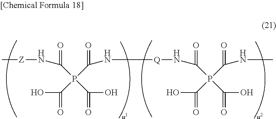
- the polyimide or polyimide precursor used in the invention is a polyimide precursor represented by the general formula (21) or a polyimide obtained by imide dehydration ring closure of the just-mentioned polyimide precursor.
- Z is at least one divalent organic group selected from the afore-indicated general formula (18) or (19), and u 1 and u 2 independently represent an integer of 1 or over, and is such that u 1 /(u 1 +u 2 ) ⁇ 0.2 is satisfied).
- the group of Z contains a tertiary arylamine skeleton and may serve as a charge transporting site and is introduced so as to mainly improve a charge injection efficiency of thin film.
- the value of u 1 /(u 1 +u 2 ) in the formula (21) is preferably at 0.2, more preferably at 0.5 and most preferably at 0.8 as a lower limit thereof.
- W′ represents a hydrogen atom, fluorine, an alkyl group that has 1 to 8 carbon atoms and may be branched, or an alkoxy group that has 1 to 8 carbon atoms and may be branched).
- the method of preparing the polyimide or polyimide precursor used in the charge transporting varnish of the invention is not limited to a specific one.
- the method of preparing the polyimide precursor mention is made, for example, of a method wherein tetracarboxylic acid and a derivative thereof, and a primary diamine are polymerized.
- the method of preparing a polyimide mention is made, for example, of a method in which the polyimide precursor obtained by the above method is thermally dehydrated at 100 to 400° C., or a method in which chemical imidization is carried out by use of a conventionally employed imidization catalyst such as of triethylamine/acetic anhydride. In order to ensure solubility in these methods, part of a polyimide precursor may be left without imidization.
- tetracarboxylic acid derivative used for the preparation of the polyimide precursor, it is usual to use tetracarboxylic acid dianhydride.
- the ratio of the total moles of a primary amine to the total moles of tetracarboxylic acid dianhydride is preferably 0.80 to 1.20. If the primary amine is used in excess, the resulting solution may be densely colored in some case, and if an acid anhydride is used in excess, an unstable structure such as of an anhydride-terminal polyimide precursor may occur. Taking these into consideration, the ratio of the total moles of the primary amine is more preferably 1.05 to 1.10. Like an ordinary polycondensation reaction, as the ratio of the total moles is closer to 1, the resulting polymer has a greater degree of polymerization.
- the number average molecular weight of the polyimide or polyimide precursor is preferably at 1,000 to 50,000, more preferably at 5,000 to 30,000.
- the method of polymerization by reaction between a tetracarboxylic acid dianhydride and a primary diamine is not critical.
- NMP N-methyl-2-pyrrolidone
- DMAc N,N-dimethylacetamide
- DMF N,N-dimethylformamide
- the reaction temperature may be arbitrarily selected from a temperature range of ⁇ 20 to 150° C., preferably ⁇ 5 to 100° C.
- tetracarboxylic acid and derivatives thereof used to obtain the polyimide or polyimide precursor include: aromatic tetracarboxylic acids, and dianhydrides thereof and their dicarboxylic acid diacid halides such as pyromellitic acid, 2,3,6,7-naphthalenetetracarboxylic acid, 1,2,5,6-naphthalenetetracarboxylic acid, 1,4,5,8-naphthalenetetracarboxylic acid, 3,3′,4,4′-biphenyltetracarboxylic acid, 2,3,3′,4-biphenyltetracarboxylic acid, bis(3,4-dicarboxyphenyl)ether, 3,3′,4,4′-benzophenonetetracarboxylic acid, bis(3,4-dicarboxyphenyl)sulfone, bis(3,4-dicarboxyphenyl)methane, 2,2-bis(3,4-dicarboxyphenyl)
- diamines used to obtain polyimides or polyimide precursors are not critical in type. Mention is made, for example, of: aromatic diamines such as p-phenylenediamine, m-phenylenediamine, 2,5-diaminotoluene, 2,6-diaminotoluene, 4,4′-diaminobiphenyl, 3,3′-dimethyl-4,4′-diaminobiphenyl, diaminodiphenylmethane, diaminodiphenyl ether, 2,2′-diaminodiphenylpropane, bis(3,5-diethyl-4-aminophenyl)methane, diaminodiphenylsulfone, diaminobenzophenone, diaminonaphthalene, 1,4-bis(4-aminophenoxy)benzene, 1,4-bis(4-aminophenyl)benzene, 9,10-bis(4-amin
- the solvents used to obtain the charge transporting varnish of the invention include, for example, water, methanol, DMF, DMAc, NMP, N,N′-dimethylimidazolidinone, dimethylsulfoxide, chloroform, toluene and the like although not limited thereto. These solvents may be used singly or in combination of two or more.
- a highly viscous solvent may be admixed in the charge transporting varnish of the invention for the purpose of obtaining a highly viscous varnish within a range of amount not impeding the solubility of a charge transporting substance and the like.
- the highly viscous solvent include cyclohexanol, ethylene glycol, ethylene glycol diglycidyl ether, 1,3-octylene glycol, diethylene glycol, dipropylene glycol, triethylene glycol, tripropylene glycol, 1,3-butanediol, 1,4-butanediol, propylene glycol, hexylene glycol and the like although not limited thereof.
- solvents that are capable of imparting flatness of film upon baking for the purposes of improving wettability to substrate, controlling a surface tension of solvent, controlling polarity, and controlling a boiling point may be added within a range of amount not impeding the solubility of a charge transporting substance and the like.
- Specific examples such a solvent include butyl cellosolve, diethylene glycol diethyl ether, dipropylene glycol monomethyl ether, ethyl carbitol, diacetone alcohol ⁇ -butyrolactone, ethyl lactate and the like although not limited thereto.
- the charge transporting thin film according to the invention is formed by use of such a charge transporting varnish as set out hereinabove and can be conveniently used as a hole injection layer or hole transport layer, or an electron injection layer or electron transport layer of an organic EL device.
- This thin film can be formed, for example, by coating a charge transporting varnish onto a substrate and evaporating a solved therefrom.
- the coating manner of the varnish is not critical, and many known coating methods such as a dipping method, a spin coating method, a transfer printing method, a roll coating method, an ink jet method, a spraying method, a brushing method and the like, each ensuring uniform film formation.
- the manner of evaporating a solvent is not critical, and evaporation is carried out by use of a hot plate or an oven in an appropriate atmosphere, i.e., in air or in an atmosphere of an inert gas such as nitrogen or the like, or in vacuum, thereby enabling one to obtain a thin film having a uniform film surface.
- the baking temperature is not limited to any specific one in so far as a solvent can be evaporated and is preferably at 40 to 250° C. In order to develop a more uniform film-forming property or to cause the reaction to proceed on a substrate, the temperature may be changed by two or more stages.
- the thickness of the charge transporting thin film is not critical. Where the film is used as a charge injection layer within the organic EL device, the thickness is preferably at 5 to 200 nm.
- For changing the film thickness there is used a method wherein a solid concentration in the varnish is changed, or an amount of a solution on a substrate is changed upon coating.
- the methods of fabricating an OLED device using the charge transporting varnish (charge transporting thin film) of the invention and the types of materials used are, respectively, those mentioned below although not limited thereto.
- the electrode substrate used is cleaned beforehand by subjecting to liquid cleaning with a detergent, an alcohol, pure water or the like, and with an anode substrate, it is preferable to carry out a surface treatment, such as an ozone treatment, an oxygen-plasma treatment or the like, just prior to its use. It will be noted that where an anode material is composed mainly of an organic matter, the surface treatment may not be effected.
- a hole transporting varnish is applied onto an anode substrate by such a coating method as mentioned above to form a hole transporting thin film on the anode.
- This substrate is introduced into a vacuum deposition apparatus, followed by successive deposition of a hole transporting layer, an emission layer, an electron transporting layer, an electron injection layer and a cathode metal to provide an OLED device.
- a carrier block layer may be provided between optional layers.
- ITO indium tin oxide
- IZO indium zinc oxide
- a flattened layer is preferable.
- polythiophene derivatives and polyanilines having high charge transportability may also be used.
- triarylamines such as a (triphenylamine)dimmer derivative (TPD), an ( ⁇ -naphthyldiphenylamine)dimer ( ⁇ -NPD), [(triphenylamine)dimer]spiro dimer (spiro-TAD) and the like; starburst amines such as 4,4′,4′′-tris[3-methylphenyl(phenyl)-amino]triphenylamine (m-MTDATA), 4,4′,4′′-tris[1-naphtyl(phenyl)amino]triphenylamine (1-TNATA) and the like; and oligothiophenes such as 5,5′′-bis- ⁇ 4-[bis(4-methylphenyl)amino]phenyl ⁇ -2,2′:5′,2′′-terthiophene (BMA-3T) and the like.
- TPD triphenylamine)dimmer derivative
- ⁇ -NPD ⁇ -n
- materials for forming an emission layer mention is made, for example, of tris(8-quinolilate)aluminum (III) (Alq 3 ), bis(8-quinolilate)zinc (II)(Znq 2 ), bis(2-methyl-8-quinolilate)(p-phenylphenolate)aluminum (III) (BAlq), 4,4′-bis(2,2-diphenylvinyl)biphenyl (DPVBi) and the like.
- the material for forming such a hole transporting layer as mentioned above or a material for forming an electron transporting layer mentioned hereinbefore and a light-emitting dopant may be co-deposited to form an emission layer.
- such a light-emitting dopant includes quinacridone, rubrene, coumarin 540, 4-(dicyanomethylene)-2-methyl-6-(p-dimethylaminostyryl)-4H-pyrane (DCM), tris(2-phenylpyridine)iridium (III) (Ir(ppy) 3 ) and (1,10-phenanthroline)-tris(4,4,4-trifluoro-1-(2-thienyl)-butan-1,3-dionate)europium (III) (Eu(TTS) 3 phen) and the like.
- quinacridone quinacridone
- rubrene coumarin 540
- DCM 4-(dicyanomethylene)-2-methyl-6-(p-dimethylaminostyryl)-4H-pyrane
- DCM 4-(dicyanomethylene)-2-methyl-6-(p-dimethylaminostyryl)-4H-pyrane
- DCM 4-(dicyanomethylene)-2-
- lithium oxide LiO 2
- magnesium oxide MgO
- alumina Al 2 O 3
- lithium fluoride LiF
- magnesium fluoride MgF 2
- strontium fluoride SrF 2
- Liq Li(acac)
- lithium acetate lithium benzoate and the like.
- the cathode materials include, for example, aluminum, magnesium-silver alloys, aluminum-lithium alloys, lithium, sodium, potassium, cesium and the like.
- a carrier block layer For materials forming a carrier block layer, mention is made, for example, of PBD, TAZ, BCP and the like.
- an electron transporting varnish is coated onto a cathode substrate by such a coating method as indicated hereinbefore to form an electron transporting thin film on the cathode substrate.
- This substrate is introduced into a vacuum deposition apparatus, followed by forming an electron transporting layer, an emission layer, a hole transporting layer and a hole injection layer using such materials as set out above, respectively, and forming a film of an anode material by sputtering or the like method to provide an OLED device.
- a light-emitting, charge transporting polymer layer is formed to provide a PLED device including a charge transporting thin film obtained from the charge transporting varnish of the invention.
- a hole transporting thin film is formed on an anode substrate in the same manner as for the OLED device, and a light-emitting, charge transporting polymer layer is formed on top of the thin film, followed by vacuum deposition of a cathode electrode to provide a PLED device.
- an electron transporting thin film may be formed on a cathode substrate in the same manner as for the OLED device, on top of which a light-emitting, charge transporting polymer layer formed, followed by formation of an anode electrode by a method such as sputtering, vacuum deposition, spin coating or the like to provide a PLED device.
- anode and cathode materials those exemplified with respect to the OLED device may be likewise used. Cleaning and surface treatments may be carried out in the same manner as illustrated for the OLED device.
- the method of forming a light-emitting, charge transporting polymer layer is one wherein a solvent is added to a light-emitting, charge transporting polymer material or a material obtained by adding a light-emitting dopant thereto for dissolution or dispersion, followed by coating onto an electrode substrate which has been formed with a hole injection layer beforehand and evaporating the solvent to from a film.
- polyfluorene derivatives such as a poly(9,9-dialkylfluorene) (PDAF) and the like
- polyphenylenevinylene derivatives such as poly(2-methoxy-5-(2′-ethylhexoxy)-1,4-phenylenevinylene) (MEH-PPV) and the like
- polythiophene derivatives such as a poly(3-alkylthiophene) (PAT) and the like
- PVCz polyvinylcarbazole
- the solvent includes toluene, xylene, chloroform or the like.
- a dissolution or uniform dispersion method those methods such as, for example, agitation, heated agitation, ultrasonic dispersion and the like may be mentioned.
- the coating method is not critical and includes, for example, a dipping method, a spin coating method, a transfer printing method, a roll coating method, an ink jet method, a spraying method, a brushing method and the like, and coating is preferably carried out in an inert gas such as nitrogen, argon or the like.
- a method of evaporating a solvent mention is made, for example, of a method of heating in an inert gas or in vacuum with use of an oven or hot plate.
- the viscosity was measured by means of an E-type viscometer (ELD-50, made by Tokyo Keiki Co., Ltd.) and the molecular weight of polymer was measured by use of a GPC apparatus (SSC-7200, made by Senshu Scientific Co., Ltd.) equipped with a GPC column (KD-803/KD-805, made by Shodex).
- E-type viscometer ELD-50, made by Tokyo Keiki Co., Ltd.
- GPC apparatus SSC-7200, made by Senshu Scientific Co., Ltd.
- KD-803/KD-805 made by Shodex
- the film thickness was measured by a surface profile measuring apparatus (DEKTAK3ST, made by Ulvac, Inc.) and the surface roughness was measured by use of an atomic force microscope (AFM) (Nanoscope (registered trade mark) IIIa, made by Veeco Instruments).
- AFM atomic force microscope
- the device characteristics such as luminance, current density, efficiency and the like were measured by use of an organic EL emission efficiency measuring apparatus (EL-1003, made by Precise Gauges Co., Ltd.) and the measurement of electric conductivity was performed by use of a semiconductor parameter analyzer (4156C, made by Agilent Technologies).
- a visible light-UV absorption spectrum measuring apparatus UV-3100PC, made by Simadzu Corporation was used.
- PTA phenyltetraaniline
- DDE 4,4′-diaminodiphenyl ether
- PMDA anhydrous pyromellitic acid
- the thin film formation of the varnish on an ITO glass substrate was carried out in the following manner.
- the ITO glass substrate was subjected to ozone cleaning over 40 minutes until just before application of the varnish by spin coating.
- the above-prepared varnish (A1) was coated onto the ITO glass substrate by a spin coating method and baked in air at 200° C. for 1 hour to provide a 30 nm thick uniform thin film.
- the electric conductivity of the thus obtained film upon current passage of 100 mA/cm 2 was at 3.1 ⁇ 10 ⁇ 7 Scm ⁇ 1 .
- the thus obtained varnish (C) was coated onto an ITO glass substrate according to the method described in Example 1 and baked in air at 200° C. for 1 hour to provide 30 nm thick uniform thin films.
- the electric conductivity of the thus obtained thin film upon current passage of 100 mA/cm 2 was at 3.6 ⁇ 10 ⁇ 7 Scm ⁇ 1 .
- the varnishes obtained in Examples 1 to 3 were, respectively, formed as a hole transporting thin film on an ITO glass substrate according to the method described in Example 1, followed by introduction within a vacuum deposition apparatus and successive deposition of ⁇ -NPD, Alq 3 , LiF and Al.
- the film thicknesses were, respectively, at 40 nm, 60 nm, 0.5 nm and 100 nm, and vacuum deposition operations were started for each case when a pressure reached 8 ⁇ 10 ⁇ 4 Pa or below.
- the deposition rate was set at 0.3 to 0.4 nm/s except for LiF and that of LiF was set at 0.02 to 0.04 nm/s.
- the moving operation between the deposition operation cycles was performed in vacuum.
- the characteristics of the resulting OLED devices are shown in Table 1.
- the varnish (C) obtained in Comparative Example 1 was coated as a hole transporting thin film on an ITO glass substrate according to the method described in Example 1, followed by introduction of a vacuum deposition apparatus and successive deposition of ⁇ -NPD, Alq 3 , LiF and Al.
- the respective film thicknesses were at 40 nm, 60 nm, 0.5 nm and 100 nm, and the deposition operation was carried out after the pressure arrived at 8 ⁇ 10 ⁇ 4 Pa or below and the deposition rate was at 0.3 to 0.4 nm/s except for LiF and at 0.02 to 0.04 nm/s for LiF.
- the moving operation between the vacuum deposition cycles was performed in vacuum.
- the characteristics of the resulting OLED device are shown in Table 1.
- the varnishes (A1) and (A3) obtained in Examples 1 and 2 were coated, according to a spin coating method, on a quartz substrate that had been subjected to ozone cleaning for 40 minutes until just before the spin coating and baked in air at 200° C. for 1 hour to provide a 30 nm thick uniform thin film.
- the resulting substrate was subjected to measurement of a transmittance by use of a UV-visible absorption spectrum (UV/VIS spectrum) apparatus.
- UV/VIS spectrum UV-visible absorption spectrum
- the varnishes (B1) and (B2) obtained in Example 3 were coated, by spin coating, on a quartz substrate that had been subjected to ozone cleaning over 40 minutes until just before the spin coating and baked in air at 200° C. for 1 hour to provide a 30 nm thick uniform thin film.
- the resulting substrate was subjected to measurement of transmittance by use of a visible-UV absorption spectrum (UV/VIS spectrum) apparatus.
- the resulting transmission spectrum is shown in FIG. 2 .
- the varnish (C) obtained in Comparative Example 1 was coated onto a quartz substrate according to the method described in Example 5 and baked in air at 200° C. for 1 hour to provide a 30 nm thick uniform thin film.
- the resulting substrate was subjected to measurement of transmittance by use of a visible-UV absorption spectrum (UV/VIS spectrum) apparatus.
- the resulting transmission spectrum is shown in FIG. 3 .
- TPD-DA N,N′-diphenyl-N,N′-di(4-(aminophenoxy)phenyl)benzidine
- TPD-DA N,N′-diphenyl-N,N′-di(4-(aminophenoxy)phenyl)benzidine
- p-phenylenediamine 0.13 g (1.2 mmols) of p-phenylenediamine
- PI-x1 polyamic acid
- Mn number average molecular weight
- Mw weight average molecular weight
- TPD-DA used in the above Synthetic Examples 4 to 6 and represented by the following formula was synthesized according to a procedure set out in WO 02/100949.
- the thus obtained varnish was formed as a thin film on an ITO glass substrate according to the following procedure.
- the varnish (X1) was coated, according to a spin coating method, onto an ITO glass substrate that had been subjected to ozone cleaning over 40 minutes until just before spin coating of the varnish, followed by baking in air at 200° C. for 1 hour to provide a 30 nm thick uniform thin film.
- the electric conductivity of the thin film upon passage of an electric current of 100 mA/cm 2 was found to be 4.8 ⁇ 10 ⁇ 7 Scm ⁇ 1 .
- varnish (X3) having a solid concentration of 5% was prepared.
- the thus obtained varnish was coated onto an ITO substrate in the same manner as in Example 7 and baked in air at 200° C. for 1 hour to provide a 30 nm thick uniform thin film.
- the electric conductivity of the thin film upon passage of an electric current of 100 mA/cm 2 was found to be 4.0 ⁇ 10 ⁇ 7 Scm ⁇ 1 .
- varnish (X4) having a solid concentration of 5% was prepared.
- the thus obtained varnish was coated onto an ITO substrate in the same manner as in Example 7 and baked in air at 200° C. for 1 hour to provide a 30 nm thick uniform thin film.
- the electric conductivity of the thin film upon passage of an electric current of 100 mA/cm 2 was found to be 5.2 ⁇ 10 ⁇ 7 Scm ⁇ 1 .
- the varnishes (X1-X4) obtained in Examples 7 to 10 were, respectively, formed as a hole transporting thin film on an ITO glass substrate according to the method described in Example 7, followed by introduction into a vacuum deposition apparatus and successive deposition of ⁇ -NPD, Alq 3 , LiF and Al.
- the film thicknesses were set at 40 nm, 45 nm, 0.5 nm and 100 nm, respectively, and each deposition operation was started after the pressure was arrived at 8 ⁇ 10 ⁇ 4 Pa or below, and the deposition rate was set at 0.3 to 0.4 nm/s except for LiF and at 0.02 to 0.4 nm/s for LiF.
- the moving operation between deposition cycles was carried out in vacuum.
- the characteristics of the resulting OLED device are shown in Table 2.
- the varnish (Z) obtained in Comparative Example 5 was formed as a hole transporting thin film on an ITO glass substrate according to the method described in Example 7, followed by vacuum deposition in the same manner as in Example 11 to provide an OLED device.
- the characteristics of the resulting OLED device are shown in Table 2.
- the respective OLED devices of Example 11 provided with the films prepared from the varnishes (X1 to X4) using the polyamic acids are lower in emission initiating voltage and drive voltage and higher in efficiency than the device of Comparative Example 6 provided with the film prepared from the polyamic acid-free varnish (Z). It will also be seen that the devices provided with the films prepared from the varnishes (X1 to X3) which make use of polyamic acids having a triarylamine skeleton are lower in emission initiating voltage and drive voltage than the device provided with the film prepared from the varnish (X4) using the triarylamine skeleton-free polyamic acid.
- the 10% NMP solution of the polyamic acid (PI-x3) obtained in Synthetic Example 6 was added to the DMAc solution of PTA/5-SSA prepared according to the method described in Example 7 in such a way that polyamic acid was made at 20 wt % and 30 wt % of the total solid content, followed by further addition of cyclohexanol and agitation to prepare varnishes (X5, X6) having a solid content of 5%.
- the respective varnishes (X3, X5, X6) obtained in Examples 9 and 12 were formed as a hole transporting thin film on an ITO glass substrate in the same manner as in Example 7, followed by introduction into a vacuum deposition apparatus and successive deposition of ⁇ -NPD, Alq 3 , LiF and Al.
- the film thicknesses were set at 30 nm, 40 nm, 0.5 nm and 100 nm, respectively, and each deposition operation was started after the pressure arrived at 8 ⁇ 10 ⁇ 4 Pa or below, and the deposition rate was set at 0.3 to 0.4 nm/s except for LiF and at 0.02 to 0.4 nm/s for LiF.
- the moving operation between deposition cycles was carried out in vacuum.
- the characteristics of the resulting OLED device are shown in Table 3.
- the varnish (Z) obtained in Comparative Example 5 were formed as a hole transporting thin film on an ITO glass substrate in the same manner as in Example 7, followed by vacuum deposition in the same manner as in Example 13 to provide an OLED device.
- the characteristics of the OLED device are shown in Table 3.
- the respective OLED devices of Example 13 provided with the films prepared from the varnishes (X3, X5 and X6) are lower in drive voltage than the device of Comparative Example 7 provided with the film prepared from the varnish (Z).
Landscapes
- Chemical & Material Sciences (AREA)
- Engineering & Computer Science (AREA)
- Materials Engineering (AREA)
- Organic Chemistry (AREA)
- Chemical Kinetics & Catalysis (AREA)
- Life Sciences & Earth Sciences (AREA)
- Wood Science & Technology (AREA)
- Physics & Mathematics (AREA)
- Spectroscopy & Molecular Physics (AREA)
- Medicinal Chemistry (AREA)
- Polymers & Plastics (AREA)
- Health & Medical Sciences (AREA)
- Macromolecular Compounds Obtained By Forming Nitrogen-Containing Linkages In General (AREA)
- Electroluminescent Light Sources (AREA)
- Conductive Materials (AREA)
- Compositions Of Macromolecular Compounds (AREA)
Abstract
Description
- Non-patent Document 1:
- Applied Physics Letters, U.S.A. 1987, Vol. 51, pp. 913 to 915
- Non-patent Document 2:
- Applied Physics Letters, U.S.A. 1996, Vol. 69, pp. 2160 to 2162
- Non-patent Document 3:
- Nature, U.K. 1992, Vol. 357, pp. 477 to 479
- Non-patent Document 4:
- Applied Physics Letters, U.S.A. 1994, Vol. 64, pp. 1245 to 1247
- Non-patent Document 5:
- Applied Physics Letters, U.S.A. 1998, Vol. 72, pp. 2660 to 2662
- Patent Document 1:
- JP-A 11-185962
[2] The charge transporting varnish of [1], wherein the charge transporting substance is made of an oligoaniline derivative represented by the general formula (1) or a quinonediimine derivative that is an oxidized product of the general formula (1)

[wherein R1, R2 and R3 independently represent hydrogen, a monovalent hydrocarbon group or an organoxy group, A and B independently represent a divalent group represented by the general formula (2) or (3)

(wherein R4 to R11 independently represent hydrogen, a hydroxyl group, a monovalent hydrocarbon group, an organoxy group, an acyl group or a sulfone group, and m and n are independently an integer of 1 or over, and is such that m+n≦20 is satisfied)].
[3] The charge transporting varnish of [2], wherein the charge transporting substance is made of an oligoaniline derivative represented by the general formula (4) or a quinonediimine derivative that is an oxidized product of the general formula (4)

(wherein R1 to R7, m and n, respectively, have the same meanings as defined above).
[4] The charge transporting varnish of [3], wherein m and n is such that m+n≦6 is satisfied.
[5] The charge transporting varnish of any one of [1] to [4], wherein the polymer is contained in 0.1 to 50 wt % based on the total weight of solids in the charge transporting varnish.
[6] The charge transporting varnish of any one of [1] to [5], wherein the polymer is made of a polyimide or polyimide precursor having a number average molecular weight of 1000 to 50000.
[7] The charge transporting varnish of any one of [1] to [6], wherein the polymer is made of a polyimide precursor represented by the general formula (5), or a polyimide obtained by dehydration ring closure of the polyimide precursor

{wherein P is at least one tetravalent organic group selected from those of the general formulas (6) to (12)

[in the formula (6), R12 to R15 independently represent hydrogen, fluorine, an alkyl group that has 1 to 5 carbon atoms and may have a branched structure, or an alkoxy group that has 1 to 5 carbon atoms and may have a branched structure], Q is at least one divalent organic group selected from those of the general formulas (13) to (19)

[wherein R16 to R32 independently represent hydrogen, fluorine, an alkyl group that has 1 to 5 carbon atoms and may have a branched structure, or an alkoxy group that has 1 to 5 carbon atoms and may have a branched structure, X independently represents —O—, —S—, —C(O)NH—, —NHC(O)—, an alkylene group that has 1 to 5 carbon atoms and may have a branched structure, or an alkylenedioxo group that has 1 to 5 carbon atoms and may have a branched structure, Y represents a group of the general formula (20)

(wherein X has the same meaning as defined above, and j is 0 or 1),

(wherein P and Q, respectively, have the same meanings as defined above, Z is at least one divalent organic group selected from the general formula (18) or (19), u1 and u2 are independently an integer of 1 or over, and is such that u1/(u1+u2)≧0.2 is satisfied).
[9] The charge transporting varnish of [8], wherein the Z is at least one divalent organic group selected from those of the general formulas (22) to (27)

(wherein W′ represents a hydrogen atom, fluorine, an alkyl group that has 1 to 8 carbon atoms and may have a branched structure or an alkoxy group that has 1 to 8 carbon atoms and may have a branched structure).
[10] The charge transporting thin film formed by use of the charge transporting varnish of any one of [1] to [9].
[11] The organic electroluminescent device including at least one layer made of the charge transporting thin film of [10].

[wherein R1, R2 and R3 independently represent hydrogen, a monovalent hydrocarbon group or an organoxy group, and A and B independently represent a divalent group represented by the general formula (2) or (3)

(wherein R4 to R11 independently represent hydrogen, a hydroxyl group, a monovalent hydrocarbon group, an organoxy group, an acyl group or a sulfone group, and m and n are independently an integer of 1 or over, and is such that m+n≦20 is satisfied)].

(wherein R1 to R7, m and n, respectively, have the same meanings as defined above).

(wherein D represents a benzene ring, a naphthalene ring, an anthracene ring, a phenanthrene ring or a heterocyclic ring, and R33 and R34 independently represent a carboxyl group or a hydroxyl group).


[wherein R12 to R15 independently represent hydrogen, fluorine, an alkyl group that has 1 to 5 carbon atoms and may be branched, or an alkoxy group that has 1 to 5 carbon atoms and may be branched].


(wherein X has the same meaning as defined above and j is 0 or 1).
(wherein P and Q, respectively, have the same meanings as defined before, Z is at least one divalent organic group selected from the afore-indicated general formula (18) or (19), and u1 and u2 independently represent an integer of 1 or over, and is such that u1/(u1+u2)≧0.2 is satisfied).

(wherein W′ represents a hydrogen atom, fluorine, an alkyl group that has 1 to 8 carbon atoms and may be branched, or an alkoxy group that has 1 to 8 carbon atoms and may be branched).


| TABLE 1 | ||||
| Ratio | On passage of an electric | |||
| of | Emission | current of 50 mA/cm2 | ||
| poly- | initiating | Volt- | Current | ||||
| Var- | imide | voltage | age | Luminance | efficiency | ||
| nish | (wt %) | (V) | (V) | (cd/cm2) | (cd/A) | ||
| Exam- | A2 | 3 | 2.8 | 8.3 | 2790 | 5.6 |
| ple 4 | A1 | 10 | 3.0 | 8.6 | 3320 | 6.6 |
| A3 | 15 | 3.0 | 8.9 | 2760 | 5.5 | |
| A4 | 20 | 3.3 | 9.4 | 2600 | 5.3 | |
| B1 | 10 | 2.8 | 8.9 | 3100 | 6.2 | |
| B2 | 15 | 2.8 | 8.9 | 2800 | 5.6 | |
| Compar- | C | 0 | 3.3 | 9.7 | 2500 | 5.0 |
| ative | ||||||
| Exam- | ||||||
| ple 3 | ||||||

| TABLE 2 | |||
| On passage of an electric | |||
| Emission | current of 50 mA/cm2 | ||
| Poly- | initiating | Volt- | Current | ||||
| Var- | imide | voltage | age | Luminance | efficiency | ||
| nish | species | (V) | (V) | (cd/cm2) | (cd/A) | ||
| Exam- | X1 | PI-x1 | 2.8 | 8.1 | 1670 | 1.3 |
| ple 11 | X2 | PI-x2 | 2.8 | 7.7 | 1630 | 1.3 |
| X3 | PI-x3 | 2.8 | 7.5 | 1600 | 1.3 | |
| X4 | PI-b | 3.0 | 8.5 | 1710 | 1.3 | |
| Compar- | Z | nil | 3.0 | 8.9 | 1380 | 1.0 |
| ative | ||||||
| Exam- | ||||||
| ple 6 | ||||||
| * The respective polyamic acids were contained in an amount of 10 wt % based on the total solid content of varnish. | ||||||
| TABLE 3 | |||||
| Emis- | On passage of an electric | ||||
| Ratio | sion | current of 50 mA/cm2 | |||
| of | initi- | Current | ||||||
| poly- | Poly- | ating | Volt- | Lumi- | effi- | |||
| Var- | imide | imide | voltage | age | nance | ciency | ||
| nish | (wt %) | species | (V) | (V) | (cd/m2) | (lm/W) | ||
| Exam- | X3 | 10 | PI-x3 | 2.8 | 6.8 | 2440 | 2.2 |
| ple 13 | X5 | 20 | PI-x3 | 2.8 | 7.3 | 2060 | 1.8 |
| X6 | 30 | PI-x3 | 2.8 | 7.4 | 1880 | 1.6 | |
| Compar- | Z | 0 | nil | 2.8 | 7.7 | 2150 | 1.7 |
| ative | |||||||
| Exam- | |||||||
| ple 7 | |||||||
Claims (10)


Applications Claiming Priority (3)
| Application Number | Priority Date | Filing Date | Title |
|---|---|---|---|
| JP2004088725 | 2004-03-25 | ||
| JP2004-088725 | 2004-03-25 | ||
| PCT/JP2005/005347 WO2005092984A1 (en) | 2004-03-25 | 2005-03-24 | Charge-transporting varnish and organic electro- luminescent devices made by using the same |
Publications (2)
| Publication Number | Publication Date |
|---|---|
| US20070187672A1 US20070187672A1 (en) | 2007-08-16 |
| US8822039B2 true US8822039B2 (en) | 2014-09-02 |
Family
ID=35056163
Family Applications (1)
| Application Number | Title | Priority Date | Filing Date |
|---|---|---|---|
| US10/593,772 Expired - Fee Related US8822039B2 (en) | 2004-03-25 | 2005-03-24 | Charge-transporting varnish and organic electro-luminescent devices made by using the same |
Country Status (7)
| Country | Link |
|---|---|
| US (1) | US8822039B2 (en) |
| EP (1) | EP1728827A4 (en) |
| JP (1) | JP5110257B2 (en) |
| KR (1) | KR101166087B1 (en) |
| CN (1) | CN1954031B (en) |
| TW (1) | TWI395802B (en) |
| WO (1) | WO2005092984A1 (en) |
Families Citing this family (17)
| Publication number | Priority date | Publication date | Assignee | Title |
|---|---|---|---|---|
| TW200400243A (en) * | 2002-02-20 | 2004-01-01 | Nissan Chemical Ind Ltd | Organic conductive material and conductive varnish |
| JP5110257B2 (en) | 2004-03-25 | 2012-12-26 | 日産化学工業株式会社 | Charge transporting varnish and organic electroluminescence device using the same |
| KR101317802B1 (en) * | 2005-06-03 | 2013-10-15 | 닛산 가가쿠 고교 가부시키 가이샤 | Charge-transporting varnishes containing charge-transporting polymers and organic electroluminescent devices made by using the same |
| KR101413129B1 (en) * | 2005-10-28 | 2014-07-01 | 닛산 가가쿠 고교 가부시키 가이샤 | Charge-transporting varnish for spray or inkjet application |
| JP4629715B2 (en) * | 2006-12-06 | 2011-02-09 | 韓國電子通信研究院 | OLED element |
| JP5133944B2 (en) * | 2009-06-11 | 2013-01-30 | 日東電工株式会社 | Resin composition and semiconductive member |
| JP5857743B2 (en) * | 2009-10-30 | 2016-02-10 | 三菱化学株式会社 | Polymer, electronic device material, composition for electronic device, organic electroluminescent device, organic solar cell device, display device and lighting device |
| US9299932B2 (en) * | 2011-12-28 | 2016-03-29 | Sony Corporation | Solid-state assembly of layers and an electric device comprising such assembly |
| JP6167606B2 (en) * | 2013-03-28 | 2017-07-26 | 株式会社デンソー | Method for producing functional film and method for producing organic EL element |
| JP6488616B2 (en) * | 2013-10-04 | 2019-03-27 | 日産化学株式会社 | Charge transporting thin film forming varnish, charge transporting thin film and organic electroluminescent device |
| JP6492564B2 (en) * | 2014-02-13 | 2019-04-03 | Jsr株式会社 | Liquid Crystal Alignment Agent, Liquid Crystal Alignment Film, Liquid Crystal Display Element, Retardation Film, Method of Producing Retardation Film, Polymer, and Compound |
| US20170133589A1 (en) * | 2014-03-28 | 2017-05-11 | Nissan Chemical Industries, Ltd. | Fluorene derivative and use thereof |
| CN107428676B (en) * | 2015-02-24 | 2022-11-08 | 日产化学工业株式会社 | Aniline derivative and use thereof |
| DE102016112975A1 (en) * | 2016-07-14 | 2018-01-18 | Osram Oled Gmbh | Inkjet printable composition, organic optoelectronic component and method for producing an optoelectronic component |
| CN110226239B (en) * | 2017-01-18 | 2022-08-09 | 日产化学株式会社 | Charge-transporting varnish and charge-transporting film using same |
| EP3731291A4 (en) * | 2017-12-20 | 2021-09-29 | Nissan Chemical Corporation | Charge-transporting varnish and charge-transporting thin film |
| WO2023120304A1 (en) * | 2021-12-22 | 2023-06-29 | 三菱瓦斯化学株式会社 | Semiconductor resin material, molded article thereof, use thereof, and flexible printed material |
Citations (32)
| Publication number | Priority date | Publication date | Assignee | Title |
|---|---|---|---|---|
| US4851487A (en) | 1988-02-22 | 1989-07-25 | Lockheed Corporation | Conductive polymer materials and method of producing same |
| US4855361A (en) | 1988-02-22 | 1989-08-08 | Lockheed Corporation | Conductive polymer-polyimide blends and method for producing same |
| WO1990011317A1 (en) | 1989-03-20 | 1990-10-04 | Lockheed Corporation | Conductive polymer-maleimide blends and method of producing same |
| US5095076A (en) | 1990-11-05 | 1992-03-10 | Lockheed Corporation | Preparation of highly soluble conductive polymer materials |
| EP0528178A2 (en) | 1991-08-16 | 1993-02-24 | International Business Machines Corporation | Electrically conductive polymeric materials and use thereof |
| JPH06338392A (en) | 1993-05-28 | 1994-12-06 | Toppan Printing Co Ltd | Organic thin film el element |
| JPH0790179A (en) | 1993-09-21 | 1995-04-04 | Tomoegawa Paper Co Ltd | Composite molding and its production |
| JPH08143664A (en) | 1994-11-16 | 1996-06-04 | Nitto Chem Ind Co Ltd | Aniline-based electrically conductive polymeric film and its production |
| JPH08259810A (en) | 1995-03-27 | 1996-10-08 | Nitto Denko Corp | Electrically semiconductor resin sheet and its production |
| JPH10308280A (en) | 1997-05-09 | 1998-11-17 | Minolta Co Ltd | Electroluminescent element |
| JPH11116676A (en) | 1997-10-17 | 1999-04-27 | Nissan Chem Ind Ltd | Diamine containing oligoaniline unit and polyimide |
| JPH11135262A (en) | 1997-10-27 | 1999-05-21 | Mitsubishi Chemical Corp | Organic electroluminescent element |
| JPH11185962A (en) | 1997-09-05 | 1999-07-09 | Koto Gijutsu Kenkyuin Kenkyu Kumiai | Electroluminescent element having organic thin film layer containing polyimide |
| JPH11199864A (en) | 1997-10-10 | 1999-07-27 | Koto Gijutsu Kenkyuin Kenkyu Kumiai | Production of electroluminescence device |
| JP2000044683A (en) | 1998-07-29 | 2000-02-15 | Nissan Chem Ind Ltd | Diamine having oligo-aniline unit and polyimide |
| JP2001247525A (en) | 2000-03-06 | 2001-09-11 | Ricoh Co Ltd | Aromatic polycarbonate resin and electrophotographic photoreceptor |
| US6337404B1 (en) | 1998-12-17 | 2002-01-08 | Nessdisplay Co., Ltd. | Diamine hole transport agent and organic electroluminescent device containing same |
| EP1248497A1 (en) | 1999-12-02 | 2002-10-09 | Nissan Chemical Industries, Ltd. | Electroluminescence element |
| WO2002100949A1 (en) | 2001-06-12 | 2002-12-19 | Nissan Chemical Industries, Ltd. | Liquid crystal orientation agents and liquid crystal display device with the use thereof |
| JP2003077668A (en) | 2001-08-31 | 2003-03-14 | Ricoh Co Ltd | Organic thin film el element |
| US20030097003A1 (en) | 2001-04-20 | 2003-05-22 | Lindsay Geoffrey A. | Monomers for polyimides having an unusually low and tunable electrical resistivity |
| US20030105270A1 (en) | 2001-04-20 | 2003-06-05 | Lindsay Geoffrey A. | Polyimides having an unusually low and tunable electrical resistivity useful for electrical and optical applications |
| JP2003226765A (en) | 2002-12-16 | 2003-08-12 | Nitto Denko Corp | Semiconductive resin sheet and its production method |
| WO2003071559A1 (en) | 2002-02-20 | 2003-08-28 | Nissan Chemical Industries, Ltd. | Organic conductive material and conductive varnish |
| US6632544B1 (en) * | 1999-02-23 | 2003-10-14 | Junji Kido | Aromatic amine derivative, soluble conductive compound, and electroluminscent element |
| JP2004002740A (en) | 2002-03-22 | 2004-01-08 | Mitsubishi Chemicals Corp | Polymer compound, 1,4-phenylenediamine derivative, charge-transporting material, organic electroluminescent element material and organic electroluminescent element |
| JP2005041915A (en) | 2003-07-23 | 2005-02-17 | Fuji Xerox Co Ltd | Method for purifying charge-transporting polymer material, charge-transporting polymer material, and organic electroluminescent element |
| JP2005075948A (en) | 2003-09-01 | 2005-03-24 | Mitsubishi Chemicals Corp | Polymer compound, hole injection, transport material, organic electroluminescent element material, and organic electroluminescent element |
| JP2005093427A (en) | 2003-08-14 | 2005-04-07 | Mitsubishi Chemicals Corp | Composition for organic electroluminescent element, and manufacturing method of organic electroluminescent element |
| JP2005093428A (en) | 2003-08-14 | 2005-04-07 | Mitsubishi Chemicals Corp | Composition for organic electroluminescent element and organic electroluminescent element |
| JP2005108828A (en) | 2003-09-11 | 2005-04-21 | Nissan Chem Ind Ltd | Electric charge transportation type varnish, electric charge transportation type thin film and organic electroluminescent element |
| WO2005092984A1 (en) | 2004-03-25 | 2005-10-06 | Nissan Chemical Industries, Ltd. | Charge-transporting varnish and organic electro- luminescent devices made by using the same |
Family Cites Families (3)
| Publication number | Priority date | Publication date | Assignee | Title |
|---|---|---|---|---|
| JP2003261767A (en) * | 2002-03-11 | 2003-09-19 | Toyobo Co Ltd | Composition and seamless belt given by using the same |
| JP2004205617A (en) * | 2002-12-24 | 2004-07-22 | Nitto Denko Corp | Semiconductive seamless belt and its manufacture method |
| US7316791B2 (en) * | 2003-12-30 | 2008-01-08 | E.I. Du Pont De Nemours And Company | Polyimide based substrate comprising doped polyaniline |
-
2005
- 2005-03-24 JP JP2006511487A patent/JP5110257B2/en not_active Expired - Fee Related
- 2005-03-24 WO PCT/JP2005/005347 patent/WO2005092984A1/en active Application Filing
- 2005-03-24 EP EP05727092A patent/EP1728827A4/en not_active Withdrawn
- 2005-03-24 KR KR1020067019245A patent/KR101166087B1/en active IP Right Grant
- 2005-03-24 US US10/593,772 patent/US8822039B2/en not_active Expired - Fee Related
- 2005-03-24 CN CN2005800156466A patent/CN1954031B/en not_active Expired - Fee Related
- 2005-03-25 TW TW094109440A patent/TWI395802B/en not_active IP Right Cessation
Patent Citations (42)
| Publication number | Priority date | Publication date | Assignee | Title |
|---|---|---|---|---|
| US4855361A (en) | 1988-02-22 | 1989-08-08 | Lockheed Corporation | Conductive polymer-polyimide blends and method for producing same |
| US4983690A (en) | 1988-02-22 | 1991-01-08 | Lockheed Corporation | Conductive polymer-maleimide blends and method of producing same |
| US4851487A (en) | 1988-02-22 | 1989-07-25 | Lockheed Corporation | Conductive polymer materials and method of producing same |
| WO1990011317A1 (en) | 1989-03-20 | 1990-10-04 | Lockheed Corporation | Conductive polymer-maleimide blends and method of producing same |
| US5095076A (en) | 1990-11-05 | 1992-03-10 | Lockheed Corporation | Preparation of highly soluble conductive polymer materials |
| US6149840A (en) | 1991-08-16 | 2000-11-21 | International Business Machines Corporation | Electrically conductive polymeric materials and use thereof |
| EP0528178A2 (en) | 1991-08-16 | 1993-02-24 | International Business Machines Corporation | Electrically conductive polymeric materials and use thereof |
| JPH06338392A (en) | 1993-05-28 | 1994-12-06 | Toppan Printing Co Ltd | Organic thin film el element |
| JPH0790179A (en) | 1993-09-21 | 1995-04-04 | Tomoegawa Paper Co Ltd | Composite molding and its production |
| JPH08143664A (en) | 1994-11-16 | 1996-06-04 | Nitto Chem Ind Co Ltd | Aniline-based electrically conductive polymeric film and its production |
| JPH08259810A (en) | 1995-03-27 | 1996-10-08 | Nitto Denko Corp | Electrically semiconductor resin sheet and its production |
| JPH10308280A (en) | 1997-05-09 | 1998-11-17 | Minolta Co Ltd | Electroluminescent element |
| US20020098378A1 (en) | 1997-09-05 | 2002-07-25 | Ness Co., Ltd. | Electroluminescent device having an organic layer including polyimide |
| JP2001023778A (en) | 1997-09-05 | 2001-01-26 | Ness Co Ltd | Electroluminescent element having organic thin film layer containing polyimide |
| JPH11185962A (en) | 1997-09-05 | 1999-07-09 | Koto Gijutsu Kenkyuin Kenkyu Kumiai | Electroluminescent element having organic thin film layer containing polyimide |
| US20020132133A1 (en) | 1997-09-05 | 2002-09-19 | Youngkyoo Kim | Electroluminescent device having an organic layer including polyimide |
| JPH11199864A (en) | 1997-10-10 | 1999-07-27 | Koto Gijutsu Kenkyuin Kenkyu Kumiai | Production of electroluminescence device |
| JPH11116676A (en) | 1997-10-17 | 1999-04-27 | Nissan Chem Ind Ltd | Diamine containing oligoaniline unit and polyimide |
| JPH11135262A (en) | 1997-10-27 | 1999-05-21 | Mitsubishi Chemical Corp | Organic electroluminescent element |
| JP2000044683A (en) | 1998-07-29 | 2000-02-15 | Nissan Chem Ind Ltd | Diamine having oligo-aniline unit and polyimide |
| US6337404B1 (en) | 1998-12-17 | 2002-01-08 | Nessdisplay Co., Ltd. | Diamine hole transport agent and organic electroluminescent device containing same |
| US6632544B1 (en) * | 1999-02-23 | 2003-10-14 | Junji Kido | Aromatic amine derivative, soluble conductive compound, and electroluminscent element |
| EP1248497A1 (en) | 1999-12-02 | 2002-10-09 | Nissan Chemical Industries, Ltd. | Electroluminescence element |
| JP2001247525A (en) | 2000-03-06 | 2001-09-11 | Ricoh Co Ltd | Aromatic polycarbonate resin and electrophotographic photoreceptor |
| US20030105270A1 (en) | 2001-04-20 | 2003-06-05 | Lindsay Geoffrey A. | Polyimides having an unusually low and tunable electrical resistivity useful for electrical and optical applications |
| US20030097003A1 (en) | 2001-04-20 | 2003-05-22 | Lindsay Geoffrey A. | Monomers for polyimides having an unusually low and tunable electrical resistivity |
| WO2002100949A1 (en) | 2001-06-12 | 2002-12-19 | Nissan Chemical Industries, Ltd. | Liquid crystal orientation agents and liquid crystal display device with the use thereof |
| EP1403325A1 (en) | 2001-06-12 | 2004-03-31 | Nissan Chemical Industries, Ltd. | Liquid crystal orientation agents and liquid crystal display device with the use thereof |
| US20040167314A1 (en) | 2001-06-12 | 2004-08-26 | Tomohisa Yamada | Liquid crystal orientation agents and liquid crystal display device with the use thereof |
| JP2003077668A (en) | 2001-08-31 | 2003-03-14 | Ricoh Co Ltd | Organic thin film el element |
| WO2003071559A1 (en) | 2002-02-20 | 2003-08-28 | Nissan Chemical Industries, Ltd. | Organic conductive material and conductive varnish |
| US20050082514A1 (en) | 2002-02-20 | 2005-04-21 | Takuji Yoshimoto | Organic conductive material and conductive varnish |
| EP1477993A1 (en) | 2002-02-20 | 2004-11-17 | Nissan Chemical Industries, Ltd. | Organic conductive material and conductive varnish |
| JP2004002740A (en) | 2002-03-22 | 2004-01-08 | Mitsubishi Chemicals Corp | Polymer compound, 1,4-phenylenediamine derivative, charge-transporting material, organic electroluminescent element material and organic electroluminescent element |
| JP2003226765A (en) | 2002-12-16 | 2003-08-12 | Nitto Denko Corp | Semiconductive resin sheet and its production method |
| JP2005041915A (en) | 2003-07-23 | 2005-02-17 | Fuji Xerox Co Ltd | Method for purifying charge-transporting polymer material, charge-transporting polymer material, and organic electroluminescent element |
| JP2005093427A (en) | 2003-08-14 | 2005-04-07 | Mitsubishi Chemicals Corp | Composition for organic electroluminescent element, and manufacturing method of organic electroluminescent element |
| JP2005093428A (en) | 2003-08-14 | 2005-04-07 | Mitsubishi Chemicals Corp | Composition for organic electroluminescent element and organic electroluminescent element |
| JP2005075948A (en) | 2003-09-01 | 2005-03-24 | Mitsubishi Chemicals Corp | Polymer compound, hole injection, transport material, organic electroluminescent element material, and organic electroluminescent element |
| JP2005108828A (en) | 2003-09-11 | 2005-04-21 | Nissan Chem Ind Ltd | Electric charge transportation type varnish, electric charge transportation type thin film and organic electroluminescent element |
| WO2005092984A1 (en) | 2004-03-25 | 2005-10-06 | Nissan Chemical Industries, Ltd. | Charge-transporting varnish and organic electro- luminescent devices made by using the same |
| EP1728827A1 (en) | 2004-03-25 | 2006-12-06 | Nissan Chemical Industries, Ltd. | Charge-transporting varnish and organic electro- luminescent devices made by using the same |
Non-Patent Citations (19)
| Title |
|---|
| Applied Physics Letters, 1987, vol. 51, pp. 913-915. |
| Applied Physics Letters, 1994, vol. 64, pp. 1245-1247. |
| Applied Physics Letters, 1996, vol. 69, pp. 2160-2162. |
| Applied Physics Letters, 1998, vol. 72, pp. 2660-2662. |
| Bulletin of Chemical Society of Japan, 1994, vol. 67, pp. 1749-1752. |
| International Search Report mailed Sep. 5, 2006. |
| International Search Report, dated Jun. 14, 2005, for International Application No. PCT/JP2005/005347. |
| Kotov et al., "Photogeneration and photovoltaic properties of polyimides with extended charge delocalisation in polymer chains", Synthetic Metals, vol. 121, No. 1-3, pp. 1553-1554, Mar. 15, 2001. |
| Liou et al., "Synthesis and Properties of New Aromatic Poly(amine-imide)s Derived from N,N′-Bis(4-aminophenyl)-N,N′-diphenyl-1,4-phenylenediamine", Journal of Polymer Science, vol. 40, No. 21, pp. 3815-3822, Nov. 1, 2002. |
| Liou et al., "Synthesis and Properties of New Aromatic Poly(amine-imide)s Derived from N,N'-Bis(4-aminophenyl)-N,N'-diphenyl-1,4-phenylenediamine", Journal of Polymer Science, vol. 40, No. 21, pp. 3815-3822, Nov. 1, 2002. |
| Min, G., "Conducting Polymers and Their Applications in the Film Industry-Polyaniline/Polyimide Blended Films", Synthetic Metals, vol. 102, No. 1-3, pp. 1163-1166, 1999. |
| Nalwa, Structural determination of semiconductive . . . J of Material Science, 26 (1991) p. 1683-1690. * |
| Nature, 1992, vol. 357, pp. 477-479. |
| Non-Final Office Action mailed Apr. 22, 2010 in Co-Pending U.S. Appl. No. 11/921,419. |
| Supplementary European Search Report dated Jul. 5, 2011. |
| Supplementary European Search Report mailed Jan. 7, 2010 for application No. 05727092. |
| Synthetic Metals, 1997, vol. 84, pp. 119-120. |
| U.S. Office Action, dated Dec. 13, 2011, for copending U.S. Appl. No. 11/921,419. |
| U.S. Office Action, dated Sep. 29, 2010, for copending U.S. Appl. No. 11/921,419. |
Also Published As
| Publication number | Publication date |
|---|---|
| EP1728827A1 (en) | 2006-12-06 |
| US20070187672A1 (en) | 2007-08-16 |
| CN1954031A (en) | 2007-04-25 |
| KR20070004735A (en) | 2007-01-09 |
| TW200540253A (en) | 2005-12-16 |
| JP5110257B2 (en) | 2012-12-26 |
| EP1728827A4 (en) | 2010-02-03 |
| WO2005092984A1 (en) | 2005-10-06 |
| CN1954031B (en) | 2010-06-09 |
| JPWO2005092984A1 (en) | 2008-02-14 |
| KR101166087B1 (en) | 2012-07-23 |
| TWI395802B (en) | 2013-05-11 |
Similar Documents
| Publication | Publication Date | Title |
|---|---|---|
| US8822039B2 (en) | Charge-transporting varnish and organic electro-luminescent devices made by using the same | |
| US20090058269A1 (en) | Charge-transporting varnishes containing charge-transporting polymers and organic electroluminescent devices made by using the same | |
| US8298444B2 (en) | Oligoaniline compound | |
| US9172043B2 (en) | Charge-transporting varnish for spray or ink jet application | |
| JP4591681B2 (en) | Charge transport varnish | |
| EP2062870B1 (en) | Oligoaniline compounds | |
| US6821648B2 (en) | Electroluminescent element | |
| EP2246325B1 (en) | Arylsulfonic acid compound and use thereof as electron-acceptor material | |
| US7771842B2 (en) | 1,4-benzodioxane sulfonic acid compound and use thereof as electron-acceptor material | |
| JP5024498B2 (en) | Charge transporting varnish, charge transporting thin film, and organic electroluminescence device | |
| US8575392B2 (en) | Charge-transporting varnish | |
| US10069075B2 (en) | Charge-transporting varnish | |
| JP2013163710A (en) | Polyimide precursor, polyimide, charge transport composition, and method for producing polyimide precursor |
Legal Events
| Date | Code | Title | Description |
|---|---|---|---|
| AS | Assignment |
Owner name: NISSAN CHEMICAL INDUSTRIES, LTD., JAPAN Free format text: ASSIGNMENT OF ASSIGNORS INTEREST;ASSIGNORS:ONO, GO;KATO, TAKU;MAEDA, SHINICHI;REEL/FRAME:018366/0265 Effective date: 20060711 |
|
| STCF | Information on status: patent grant |
Free format text: PATENTED CASE |
|
| MAFP | Maintenance fee payment |
Free format text: PAYMENT OF MAINTENANCE FEE, 4TH YEAR, LARGE ENTITY (ORIGINAL EVENT CODE: M1551) Year of fee payment: 4 |
|
| FEPP | Fee payment procedure |
Free format text: MAINTENANCE FEE REMINDER MAILED (ORIGINAL EVENT CODE: REM.); ENTITY STATUS OF PATENT OWNER: LARGE ENTITY |
|
| LAPS | Lapse for failure to pay maintenance fees |
Free format text: PATENT EXPIRED FOR FAILURE TO PAY MAINTENANCE FEES (ORIGINAL EVENT CODE: EXP.); ENTITY STATUS OF PATENT OWNER: LARGE ENTITY |
|
| STCH | Information on status: patent discontinuation |
Free format text: PATENT EXPIRED DUE TO NONPAYMENT OF MAINTENANCE FEES UNDER 37 CFR 1.362 |
|
| FP | Lapsed due to failure to pay maintenance fee |
Effective date: 20220902 |