US8841145B2 - System for wafer-level phosphor deposition - Google Patents
System for wafer-level phosphor deposition Download PDFInfo
- Publication number
- US8841145B2 US8841145B2 US12/963,011 US96301110A US8841145B2 US 8841145 B2 US8841145 B2 US 8841145B2 US 96301110 A US96301110 A US 96301110A US 8841145 B2 US8841145 B2 US 8841145B2
- Authority
- US
- United States
- Prior art keywords
- wafer
- semiconductor wafer
- resist material
- photo resist
- dies
- Prior art date
- Legal status (The legal status is an assumption and is not a legal conclusion. Google has not performed a legal analysis and makes no representation as to the accuracy of the status listed.)
- Active
Links
Images


Classifications
-
- H—ELECTRICITY
- H01—ELECTRIC ELEMENTS
- H01L—SEMICONDUCTOR DEVICES NOT COVERED BY CLASS H10
- H01L27/00—Devices consisting of a plurality of semiconductor or other solid-state components formed in or on a common substrate
- H01L27/15—Devices consisting of a plurality of semiconductor or other solid-state components formed in or on a common substrate including semiconductor components with at least one potential-jump barrier or surface barrier specially adapted for light emission
- H01L27/153—Devices consisting of a plurality of semiconductor or other solid-state components formed in or on a common substrate including semiconductor components with at least one potential-jump barrier or surface barrier specially adapted for light emission in a repetitive configuration, e.g. LED bars
-
- H—ELECTRICITY
- H01—ELECTRIC ELEMENTS
- H01L—SEMICONDUCTOR DEVICES NOT COVERED BY CLASS H10
- H01L21/00—Processes or apparatus adapted for the manufacture or treatment of semiconductor or solid state devices or of parts thereof
- H01L21/70—Manufacture or treatment of devices consisting of a plurality of solid state components formed in or on a common substrate or of parts thereof; Manufacture of integrated circuit devices or of parts thereof
- H01L21/77—Manufacture or treatment of devices consisting of a plurality of solid state components or integrated circuits formed in, or on, a common substrate
- H01L21/78—Manufacture or treatment of devices consisting of a plurality of solid state components or integrated circuits formed in, or on, a common substrate with subsequent division of the substrate into plural individual devices
-
- H—ELECTRICITY
- H01—ELECTRIC ELEMENTS
- H01L—SEMICONDUCTOR DEVICES NOT COVERED BY CLASS H10
- H01L22/00—Testing or measuring during manufacture or treatment; Reliability measurements, i.e. testing of parts without further processing to modify the parts as such; Structural arrangements therefor
- H01L22/10—Measuring as part of the manufacturing process
-
- H—ELECTRICITY
- H01—ELECTRIC ELEMENTS
- H01L—SEMICONDUCTOR DEVICES NOT COVERED BY CLASS H10
- H01L33/00—Semiconductor devices with at least one potential-jump barrier or surface barrier specially adapted for light emission; Processes or apparatus specially adapted for the manufacture or treatment thereof or of parts thereof; Details thereof
- H01L33/005—Processes
-
- H—ELECTRICITY
- H01—ELECTRIC ELEMENTS
- H01L—SEMICONDUCTOR DEVICES NOT COVERED BY CLASS H10
- H01L33/00—Semiconductor devices with at least one potential-jump barrier or surface barrier specially adapted for light emission; Processes or apparatus specially adapted for the manufacture or treatment thereof or of parts thereof; Details thereof
- H01L33/48—Semiconductor devices with at least one potential-jump barrier or surface barrier specially adapted for light emission; Processes or apparatus specially adapted for the manufacture or treatment thereof or of parts thereof; Details thereof characterised by the semiconductor body packages
- H01L33/50—Wavelength conversion elements
- H01L33/508—Wavelength conversion elements having a non-uniform spatial arrangement or non-uniform concentration, e.g. patterned wavelength conversion layer, wavelength conversion layer with a concentration gradient of the wavelength conversion material
-
- H—ELECTRICITY
- H01—ELECTRIC ELEMENTS
- H01L—SEMICONDUCTOR DEVICES NOT COVERED BY CLASS H10
- H01L2933/00—Details relating to devices covered by the group H01L33/00 but not provided for in its subgroups
- H01L2933/0008—Processes
- H01L2933/0033—Processes relating to semiconductor body packages
- H01L2933/0041—Processes relating to semiconductor body packages relating to wavelength conversion elements
-
- H—ELECTRICITY
- H01—ELECTRIC ELEMENTS
- H01L—SEMICONDUCTOR DEVICES NOT COVERED BY CLASS H10
- H01L2933/00—Details relating to devices covered by the group H01L33/00 but not provided for in its subgroups
- H01L2933/0008—Processes
- H01L2933/0033—Processes relating to semiconductor body packages
- H01L2933/0058—Processes relating to semiconductor body packages relating to optical field-shaping elements
Definitions
- the present application relates generally to light emitting diodes, and more particularly, to a system for wafer-level phosphor deposition.
- a light emitting diode comprises a semiconductor material impregnated, or doped, with impurities. These impurities add “electrons” and “holes” to the semiconductor, which can move in the material relatively freely. Depending on the kind of impurity, a doped region of the semiconductor can have predominantly electrons or holes, and is referred to as an n-type or p-type semiconductor region, respectively.
- an LED semiconductor chip In LED applications, an LED semiconductor chip includes an n-type semiconductor region and a p-type semiconductor region. A reverse electric field is created at the junction between the two regions, which causes the electrons and holes to move away from the junction to form an active region. When a forward voltage sufficient to overcome the reverse electric field is applied across the p-n junction, electrons and holes are forced into the active region and combine. When electrons combine with holes, they fall to lower energy levels and release energy in the form of light. The ability of LED semiconductors to emit light has allowed these semiconductors to be used in a variety of lighting devices. For example, LED semiconductors may be used in general lighting devices for interior applications or in various exterior applications.
- the wafer may comprise one hundred or more dies.
- a process referred to as singulation is used to cut the dies from the wafer.
- the dies may then be coated with a phosphor coating that controls the color of the light emitted from the die when energized. After coating, the dies are probed and tested for color, light intensity output, power consumption and any other types of operational characteristics.
- coating and testing the dies after singulation may be expensive or complicated and make it difficult to obtain dies having consistent color, light intensity output, or other characteristics.
- a system for wafer-level phosphor deposition is provided to allow phosphor coating and testing to be performed on a semiconductor wafer prior to singulation.
- the system simplifies the phosphor deposition process and results in individual LED semiconductor dies having consistent operational parameters.
- a method for phosphor deposition on a semiconductor wafer comprising a plurality of LED dies comprises covering the semiconductor wafer with a selected thickness of photo resist material, removing portions of the photo resist material to expose portions of the semiconductor wafer so that electrical contacts associated with the plurality of LED dies remain unexposed, and depositing phosphor on the exposed portions of the semiconductor wafer.
- an apparatus for phosphor deposition on a semiconductor wafer comprising a plurality of LED dies.
- the apparatus comprises means for covering the semiconductor wafer with a selected thickness of photo resist material, means for removing portions of the photo resist material to expose portions of the semiconductor wafer so that electrical contacts associated with the plurality of LED dies remain unexposed, and means for depositing phosphor on the exposed portions of the semiconductor wafer.
- an LED die is provided that is prepared by a process comprising the operations of covering a semiconductor wafer comprising the LED die with a selected thickness of photo resist material, removing portions of the photo resist material to expose portions of the semiconductor wafer so that electrical contacts of the LED die remain unexposed, depositing phosphor on the exposed portions of the semiconductor wafer, removing remaining photo resist material to expose the electrical contacts of the LED die, and performing a singulation process to cut the LED die from the semiconductor wafer.
- FIG. 1 shows a side view of an exemplary LED semiconductor wafer obtained from a wafer fabrication process
- FIG. 2 shows a side view of an exemplary wafer assembly comprising the wafer of FIG. 1 attached to a carrier wafer;
- FIG. 3 shows the wafer assembly shown in FIG. 2 and further comprising a photo resist layer
- FIG. 4 shows the wafer assembly shown in FIG. 3 after removal of selected portions of the photo resist layer
- FIG. 5 shows a top view of a portion of the wafer assembly shown in FIG. 4 ;
- FIG. 6 shows the wafer assembly of FIG. 4 after deposition of a phosphor layer
- FIG. 7 shows the wafer assembly of FIG. 6 after removal of photo resist posts
- FIG. 8 shows a top view of a portion of the wafer assembly of FIG. 7 ;
- FIG. 9 shows the wafer assembly of FIG. 7 after removal of a carrier wafer
- FIG. 10 shows a singulation process performed on the wafer assembly of FIG. 7 to obtain individual LED semiconductor dies
- FIG. 11 shows an exemplary color chart that associates X and Y values with color temperature
- FIG. 12 shows an exemplary color binning graph and table used for sorting and binning LED dies
- FIG. 13 shows an exemplary method for performing wafer-level phosphor deposition
- FIG. 14 shows an exemplary apparatus for performing wafer-level phosphor deposition.
- a system for wafer-level phosphor deposition is provided to allow phosphor coating and testing to be performed on a semiconductor wafer prior to singulation.
- relative terms such as “lower” or “bottom” and “upper” or “top,” may be used herein to describe one element's relationship to another element as illustrated in the drawings. It will be understood that relative terms are intended to encompass different orientations of an apparatus in addition to the orientation depicted in the Drawings. By way of example, if an apparatus in the Drawings is turned over, elements described as being on the “lower” side of other elements would then be oriented on the “upper” sides of the other elements. The term “lower”, can therefore, encompass both an orientation of “lower” and “upper,” depending of the particular orientation of the apparatus.
- first and second may be used herein to describe various regions, layers and/or sections, these regions, layers and/or sections should not be limited by these terms. These terms are only used to distinguish one region, layer or section from another region, layer or section. Thus, a first region, layer or section discussed below could be termed a second region, layer or section, and similarly, a second region, layer or section may be termed a first region, layer or section without departing from the teachings of the present invention.
- FIG. 1 shows a side view of an exemplary LED semiconductor wafer 100 obtained from a wafer fabrication process.
- the thickness (t) of the LED wafer 100 is approximately 150 micrometers.
- the wafer 100 comprises any number of LED dies that are exposed on surface 102 .
- the LED wafer 100 may comprise one hundred or more LED dies having associated electrical contacts and light emitting regions formed on the surface 102 . During operation, the electrical contacts of each die can be energized to cause light to be emitted from the associated light emitting regions.
- FIG. 2 shows a side view of an exemplary wafer assembly 200 comprising the LED wafer 100 of FIG. 1 attached to a carrier wafer 202 .
- the carrier wafer 202 comprises a sapphire carrier wafer that is attached to the LED wafer 100 with thermal release tape 204 .
- the sapphire carrier wafer 202 operates to support the LED wafer 100 during a phosphor deposition process described below.
- the thermal release tape allows the sapphire carrier wafer 202 to be easily removed from the LED wafer 100 at a later time.
- any suitable automated assembly device is used to assemble the wafer 100 onto the carrier wafer 202 with the thermal release tape 204 .
- FIG. 3 shows a side view of a wafer assembly 300 that comprises the wafer assembly 200 and a layer of photo-resist material 302 .
- the photo-resist material 302 is a light sensitive material that becomes soluble to a photo-resist developer after being exposed to light. Any portion of the photo-resist material 302 that is unexposed to light remains insoluble to the photo-resist developer.
- the photo-resist material 302 is spin coated to form a thick layer on the LED wafer 100 .
- the photo-resist material 302 may be approximately two hundred micrometers thick. It should also be noted that any suitable photo resist deposition device may be used to apply the photo-resist material 302 to the wafer assembly 200 .
- FIG. 4 shows a side view of a wafer assembly 400 that comprises the wafer assembly 300 after removal of selected portions of the photo-resist layer 302 using a photolithography process.
- a photolithography device uses light to transfer a geometric pattern from a photo mask onto the light-sensitive photo-resist layer 302 .
- Light exposed portions of the photo-resist layer 302 are then removed by the photolithography device using a photo-resist developer leaving the unexposed portions remaining.
- the unexposed portions are illustrated as photo-resist posts 402 .
- the posts 402 are approximately two hundred micrometers tall and are located to cover the p and n electrical contact pads of all the LED dies of the LED wafer 100 .
- region 404 comprises three photo-resist posts 406 , 408 and 410 . A top view of these posts, as indicated at 412 , is described in greater detail in FIG. 5 .
- FIG. 5 shows a top view of the assembly 400 shown in FIG. 4 and provides a detailed illustration of the region 404 from the perspective of the top view indicator 412 .
- the region 404 comprises the photo-resist posts 406 , 408 and 410 that cover the p and n electrical contacts of the LED dies of the LED wafer 100 .
- the photo-resist posts 406 , 408 , and 410 may comprise any shape or geometry and are not limited to the shapes shown in FIG. 5 .
- the photo-resist posts protect these contacts from a phosphor deposition layer to be deposited on the surface 502 of the LED wafer 100 .
- the phosphor deposition operates to control the color of the light emitted by the dies of the LED wafer 100 .
- FIG. 6 shows a side view of a wafer assembly 600 that comprises the wafer assembly 300 shown in FIG. 4 after deposition of a phosphor layer 602 .
- the phosphor deposition may be performed by a deposition apparatus that utilizes any of the following techniques.
- the phosphor deposition process allows control of the thickness of phosphor layer thereby allowing control of the color of the light emitted from the LED dies. After deposition, the phosphor is allowed to cure.
- any suitable phosphor deposition process may be used to apply a phosphor layer having an appropriate thickness onto the wafer assembly 300 .
- any appropriate phosphor material may be used to achieve a resulting light emission having any desired color.
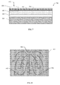
- FIG. 7 shows a side view of a wafer assembly 700 that comprises the wafer assembly 600 shown in FIG. 6 after removal of the photo-resist posts 402 .
- the photo-resists posts 402 are removed by the photolithography device by exposing the posts to light and applying the appropriate photo-resist developer.
- the phosphor layer comprises regions of phosphor 702 that cover the surface of the LED wafer 100 and cavities 704 that expose the p and n contacts through the phosphor layer. These cavities 704 allow wire bonding of the exposed contacts.
- FIG. 8 shows a top view of the assembly 700 shown in FIG. 7 and provides a detailed illustration of the region 404 from the perspective of the top view indicator 412 .
- the top view shown in FIG. 8 provides a detailed illustration of the region 404 after removal of the photo-resist posts 406 , 408 and 410 .
- the photo-resists posts Once the photo-resists posts are removed the p and n contacts underneath the posts are exposed. For example, removal of the posts 406 , 408 and 410 exposes the contacts 802 , 804 and 806 , respectively.
- the semiconductor surface which is now covered by the phosphor deposition 808 .
- FIG. 9 shows a wafer assembly 900 that comprises the wafer assembly 700 of FIG. 7 after removal of the carrier wafer.
- the thermal release tape 204 is heated to release the sapphire carrier wafer 202 so that the LED wafer 100 with phosphor deposition 702 remains.
- FIG. 10 shows a singulation process performed on the wafer assembly 900 .
- the singulation process operates to divide the LED wafer assembly 900 into individual dies.
- singulation is performed using a front-side laser scribing and breaking device that divides the LED wafer assembly 900 into individual dies (i.e., 1002 , 1004 , and 1006 ).
- FIG. 11 shows an exemplary color chart 1100 that associates two parameters (X and Y) with color temperature.
- the color chart 1100 provides X values along the horizontal axis and Y values along the vertical axis.
- an X value of 0.32 and a Y value of 0.33 correspond to a color temperature of approximately 6000 Kelvin (K).
- the color chart 1100 provides a mechanism by which the X and Y values can be used to accurately identify particular colors for the purpose of binning and sorting dies.
- the wafer 900 shown in FIG. 9 is probed and tested by a computerized probing device for the purpose of associating X and Y values with each die. Probing the entire wafer at the same time is more efficient than probing individual dies after singulation.
- each die is energized and various die characteristics are determined.
- the probing device includes contacts points that are positioned to touch the electrical contacts of each die of the wafer 900 . The electrical contacts are exposed and accessible through the cavities 704 in the phosphor deposition.
- the probing device measures color temperature, lumen output, voltage, current, and any other operating parameters associated with each die. In an aspect, the measured parameters for each die are mapped to X and Y values based on the color chart 1100 . Thus, each die is associated with it own X and Y values prior to singulation.
- FIG. 12 shows a graph 1200 and associated binning table 1202 that can be used to sort and bin LED dies prior to singulation.
- the graph 1200 defines a number of bins which each include a range of X and Y values from the color chart 1100 of FIG. 11 .
- the bin D 4 includes the X value of 0.32 and the Y value of 0.33.
- the bin D 4 shown at 1204 , is associated with a range of X and Y values that include 0.32 and 0.33, respectively.
- the ANSI color temperature of this range is also shown.
- each die is separate from the wafer during the singulation process, its associated X and Y value can be used to sort it into the appropriate bin using the binning table 1202 .
- the dies in each bin can then be place on a tape or packaged using any other packaging method, so that the resulting group of dies will have excellent color consistency.
- the dies are binned and sorted by a computerized binning device that knows the X and Y values associated with each die.
- FIG. 13 shows a method for performing wafer-level phosphor deposition in accordance with the present invention.
- the method 1300 can be used to perform phosphor deposition as described above with respect to the wafer 100 .
- a LED wafer is obtained from a fabrication process.
- the wafer 100 is obtained for the wafer-level phosphor deposition process.
- the wafer 100 comprises one hundred or more LED dies.
- a support carrier is attached to the LED wafer.
- the sapphire support carrier 202 is attached to the LED wafer using thermal release tape 204 .
- the support carrier operates to support the LED wafer during the wafer-level phosphor deposition process.
- any suitable automated assembly device is used to assemble the wafer 100 onto the carrier wafer 202 with the thermal release tape 204 .
- a photo-resist layer is applied to the LED wafer.
- the photo-resist layer is applied using a spin coating process.
- the photo-resist layer is applied to the LED wafer 100 and is approximately two hundred micrometers thick.
- any suitable photo resist deposition device may be used to apply the photo-resist material 302 to the wafer assembly 200 .
- portions of the photo-resist layer are removed so that photo resist posts cover p and n contacts of the LED wafer.
- a photolithography device uses light to transfer a geometric pattern from a photo mask to the light-sensitive photo-resist layer. Light exposed portions of the photo-resist layer are then removed using a photo-resist developer leaving the unexposed portions remaining. The unexposed portions remain as photo-resist posts 402 .
- FIG. 5 shows a top view that illustrates how the photo-resist posts cover the p and n contacts of the LED wafer.
- phosphor is deposited on the surface of the LED wafer. As illustrated in FIG. 6 , phosphor is disposed on the surface of the LED wafer and surrounds the photo resist posts 402 .
- a deposition apparatus applies the phosphor to the surface of the LED wafer using at least one of a spin coating, EPD, and jetting process.
- the photo-resist posts are removed exposing the p and n contacts.
- the photo-resists posts 402 are removed by exposing them to light and applying the appropriate photo-resist developer.
- the phosphor layer comprises regions of phosphor 702 that cover the surface of the LED wafer 100 and cavities 704 that expose the p and n contacts through the phosphor layer.
- the carrier wafer is removed.
- the thermal release tape is heated to release the sapphire carrier wafer.
- any suitable automated assembly device is used to disassemble the wafer 100 from the carrier wafer 202 .
- the wafer is probed and tested to determine color temperature, lumen output, power consumption and any other LED characteristics.
- the measured color temperature of each die is associated with X and Y values according to the color chart 1100 .
- the wafer is probed and tested by a computerized probing device.
- a singulation process is performed to divide or cut the LED wafer into individual dies.
- singulation is performed using a front-side laser scribing and breaking process to divide the LED wafer 900 into individual dies.
- singulation is performed using a front-side laser scribing and breaking device that divides the LED wafer assembly 900 into individual dies.
- the dies are sorted and binned.
- the X and Y values determined during the probing and testing process at block 1316 are used to bin the dies according to the bin plot 1200 and the bin table 1202 .
- the bin plot 1200 defines one or more bins associated with X and Y values.
- the bins are further defined in the bin table 1202 .
- the X and Y value of each die is cross-referenced in the bin table 1202 to determine the bin number in which the die is to be grouped.
- the dies are binned and sorted by a computerized binning device that knows the X and Y values associated with each die.
- the method 1300 operates to perform wafer-level phosphor deposition in accordance with the present invention. It should be noted that the method 1300 is just one implementation and that the operations of the method 1300 may be rearranged or otherwise modified within the scope of the various aspects. Thus, other implementations are possible with the scope of the various aspects described.
- FIG. 14 shows an exemplary apparatus 1400 for performing wafer-level phosphor deposition.
- the apparatus 1400 is suitable for use to produce the semiconductor wafer 600 shown in FIG. 6 .
- the apparatus 1400 is implemented by one or more modules configured to provide the functions as described herein.
- each module comprises hardware and/or hardware executing software.
- the apparatus 1400 comprises a first module comprising means ( 1402 ) for covering a semiconductor wafer with a selected thickness of photo resist material, which in an aspect comprises a photo resist deposition device.
- the apparatus 1400 also comprises a second module comprising means ( 1404 ) for means for removing portions of the photo resist material to expose portions of the semiconductor wafer so that electrical contacts associated with the plurality of LED dies remain unexposed, which in an aspect comprises a photolithography device.
- the apparatus 1400 comprises a third module comprising means ( 1406 ) for means for depositing phosphor on the exposed portions of the semiconductor wafer, which in as aspect comprises a phosphor deposition apparatus.
Abstract
Description
Claims (18)
Priority Applications (6)
| Application Number | Priority Date | Filing Date | Title |
|---|---|---|---|
| US12/963,011 US8841145B2 (en) | 2010-12-08 | 2010-12-08 | System for wafer-level phosphor deposition |
| PCT/US2011/063345 WO2012078530A1 (en) | 2010-12-08 | 2011-12-05 | System for wafer-level phosphor deposition |
| CN2011800658345A CN103339720A (en) | 2010-12-08 | 2011-12-05 | System for wafer-level phosphor deposition |
| JP2013543241A JP6166659B2 (en) | 2010-12-08 | 2011-12-05 | Wafer level phosphor deposition system |
| TW100145233A TWI608522B (en) | 2010-12-08 | 2011-12-08 | System for wafer-level phosphor deposition |
| US14/479,031 US9691813B2 (en) | 2010-12-08 | 2014-09-05 | System for wafer-level phosphor deposition |
Applications Claiming Priority (1)
| Application Number | Priority Date | Filing Date | Title |
|---|---|---|---|
| US12/963,011 US8841145B2 (en) | 2010-12-08 | 2010-12-08 | System for wafer-level phosphor deposition |
Related Child Applications (1)
| Application Number | Title | Priority Date | Filing Date |
|---|---|---|---|
| US14/479,031 Continuation US9691813B2 (en) | 2010-12-08 | 2014-09-05 | System for wafer-level phosphor deposition |
Publications (2)
| Publication Number | Publication Date |
|---|---|
| US20110073896A1 US20110073896A1 (en) | 2011-03-31 |
| US8841145B2 true US8841145B2 (en) | 2014-09-23 |
Family
ID=43779315
Family Applications (2)
| Application Number | Title | Priority Date | Filing Date |
|---|---|---|---|
| US12/963,011 Active US8841145B2 (en) | 2010-12-08 | 2010-12-08 | System for wafer-level phosphor deposition |
| US14/479,031 Active US9691813B2 (en) | 2010-12-08 | 2014-09-05 | System for wafer-level phosphor deposition |
Family Applications After (1)
| Application Number | Title | Priority Date | Filing Date |
|---|---|---|---|
| US14/479,031 Active US9691813B2 (en) | 2010-12-08 | 2014-09-05 | System for wafer-level phosphor deposition |
Country Status (1)
| Country | Link |
|---|---|
| US (2) | US8841145B2 (en) |
Families Citing this family (6)
| Publication number | Priority date | Publication date | Assignee | Title |
|---|---|---|---|---|
| US8399268B1 (en) * | 2011-12-28 | 2013-03-19 | Ledengin, Inc. | Deposition of phosphor on die top using dry film photoresist |
| US9653656B2 (en) | 2012-03-16 | 2017-05-16 | Advanced Semiconductor Engineering, Inc. | LED packages and related methods |
| US8637887B2 (en) | 2012-05-08 | 2014-01-28 | Advanced Semiconductor Engineering, Inc. | Thermally enhanced semiconductor packages and related methods |
| US9059379B2 (en) | 2012-10-29 | 2015-06-16 | Advanced Semiconductor Engineering, Inc. | Light-emitting semiconductor packages and related methods |
| US9618191B2 (en) | 2013-03-07 | 2017-04-11 | Advanced Semiconductor Engineering, Inc. | Light emitting package and LED bulb |
| US9234801B2 (en) | 2013-03-15 | 2016-01-12 | Ledengin, Inc. | Manufacturing method for LED emitter with high color consistency |
Citations (18)
| Publication number | Priority date | Publication date | Assignee | Title |
|---|---|---|---|---|
| US6656574B1 (en) * | 1998-02-26 | 2003-12-02 | Micron Technology, Inc. | Structure including electrophoretically deposited patternable material for use in providing a display |
| US20060003477A1 (en) | 2002-10-30 | 2006-01-05 | Bert Braune | Method for producing a light source provided with electroluminescent diodes and comprising a luminescence conversion element |
| US20060001046A1 (en) * | 2004-07-02 | 2006-01-05 | Cree, Inc. | LED with substrate modifications for enhanced light extraction and method of making same |
| US20060157721A1 (en) * | 2005-01-11 | 2006-07-20 | Tran Chuong A | Systems and methods for producing white-light light emitting diodes |
| US20070001178A1 (en) | 2005-01-11 | 2007-01-04 | Tran Chuong A | Coating process |
| US20070222365A1 (en) * | 2004-05-18 | 2007-09-27 | Hideo Tamamura | Light-Emitting Diode and Method of Manufacturing the Same |
| US20070259509A1 (en) * | 2006-05-02 | 2007-11-08 | Chih-Ping Kuo | Method of thinning a wafer |
| US7344952B2 (en) * | 2005-10-28 | 2008-03-18 | Philips Lumileds Lighting Company, Llc | Laminating encapsulant film containing phosphor over LEDs |
| US20080179611A1 (en) * | 2007-01-22 | 2008-07-31 | Cree, Inc. | Wafer level phosphor coating method and devices fabricated utilizing method |
| US20080315228A1 (en) | 2006-06-09 | 2008-12-25 | Philips Lumileds Lighting Company, Llc | Low profile side emitting led with window layer and phosphor layer |
| US20090057701A1 (en) | 2007-08-29 | 2009-03-05 | Everlight Electronics Co., Ltd. | Phosphor coating method for fabricating light emmitting semiconductor device and applications thereof |
| US20090213294A1 (en) * | 2005-04-26 | 2009-08-27 | Samsung Electronics Co., Ltd. | Backlight unit for dynamic image and display employing the same |
| US20090272996A1 (en) | 2008-05-02 | 2009-11-05 | Cree, Inc. | Encapsulation for phosphor-converted white light emitting diode |
| US20090286335A1 (en) | 2008-05-05 | 2009-11-19 | Cree, Inc. | Methods of fabricating light emitting devices by selective deposition of light conversion materials based on measured emission characteristics |
| US20100155750A1 (en) | 2008-12-23 | 2010-06-24 | Cree, Inc. | Color correction for wafer level white LEDs |
| US20110073881A1 (en) | 2008-04-10 | 2011-03-31 | Cree, Inc | LEDs USING SINGLE CRYSTALLLINE PHOSPHOR AND METHODS OF FABRICATING SAME |
| US7939350B2 (en) * | 2008-01-03 | 2011-05-10 | E. I. Du Pont De Nemours And Company | Method for encapsulating a substrate and method for fabricating a light emitting diode device |
| US7994531B2 (en) * | 2009-04-02 | 2011-08-09 | Visera Technologies Company Limited | White-light light emitting diode chips and fabrication methods thereof |
Family Cites Families (2)
| Publication number | Priority date | Publication date | Assignee | Title |
|---|---|---|---|---|
| CN100508221C (en) | 2002-10-30 | 2009-07-01 | 奥斯兰姆奥普托半导体有限责任公司 | Method for producing a light source provided with electroluminescent diodes and comprising a luminescence conversion element |
| CN1853913B (en) | 2005-04-26 | 2011-02-09 | 宗形株式会社 | Method of dyeing or reforming injection, blow or compression moulded plastic product |
-
2010
- 2010-12-08 US US12/963,011 patent/US8841145B2/en active Active
-
2014
- 2014-09-05 US US14/479,031 patent/US9691813B2/en active Active
Patent Citations (18)
| Publication number | Priority date | Publication date | Assignee | Title |
|---|---|---|---|---|
| US6656574B1 (en) * | 1998-02-26 | 2003-12-02 | Micron Technology, Inc. | Structure including electrophoretically deposited patternable material for use in providing a display |
| US20060003477A1 (en) | 2002-10-30 | 2006-01-05 | Bert Braune | Method for producing a light source provided with electroluminescent diodes and comprising a luminescence conversion element |
| US20070222365A1 (en) * | 2004-05-18 | 2007-09-27 | Hideo Tamamura | Light-Emitting Diode and Method of Manufacturing the Same |
| US20060001046A1 (en) * | 2004-07-02 | 2006-01-05 | Cree, Inc. | LED with substrate modifications for enhanced light extraction and method of making same |
| US20060157721A1 (en) * | 2005-01-11 | 2006-07-20 | Tran Chuong A | Systems and methods for producing white-light light emitting diodes |
| US20070001178A1 (en) | 2005-01-11 | 2007-01-04 | Tran Chuong A | Coating process |
| US20090213294A1 (en) * | 2005-04-26 | 2009-08-27 | Samsung Electronics Co., Ltd. | Backlight unit for dynamic image and display employing the same |
| US7344952B2 (en) * | 2005-10-28 | 2008-03-18 | Philips Lumileds Lighting Company, Llc | Laminating encapsulant film containing phosphor over LEDs |
| US20070259509A1 (en) * | 2006-05-02 | 2007-11-08 | Chih-Ping Kuo | Method of thinning a wafer |
| US20080315228A1 (en) | 2006-06-09 | 2008-12-25 | Philips Lumileds Lighting Company, Llc | Low profile side emitting led with window layer and phosphor layer |
| US20080179611A1 (en) * | 2007-01-22 | 2008-07-31 | Cree, Inc. | Wafer level phosphor coating method and devices fabricated utilizing method |
| US20090057701A1 (en) | 2007-08-29 | 2009-03-05 | Everlight Electronics Co., Ltd. | Phosphor coating method for fabricating light emmitting semiconductor device and applications thereof |
| US7939350B2 (en) * | 2008-01-03 | 2011-05-10 | E. I. Du Pont De Nemours And Company | Method for encapsulating a substrate and method for fabricating a light emitting diode device |
| US20110073881A1 (en) | 2008-04-10 | 2011-03-31 | Cree, Inc | LEDs USING SINGLE CRYSTALLLINE PHOSPHOR AND METHODS OF FABRICATING SAME |
| US20090272996A1 (en) | 2008-05-02 | 2009-11-05 | Cree, Inc. | Encapsulation for phosphor-converted white light emitting diode |
| US20090286335A1 (en) | 2008-05-05 | 2009-11-19 | Cree, Inc. | Methods of fabricating light emitting devices by selective deposition of light conversion materials based on measured emission characteristics |
| US20100155750A1 (en) | 2008-12-23 | 2010-06-24 | Cree, Inc. | Color correction for wafer level white LEDs |
| US7994531B2 (en) * | 2009-04-02 | 2011-08-09 | Visera Technologies Company Limited | White-light light emitting diode chips and fabrication methods thereof |
Also Published As
| Publication number | Publication date |
|---|---|
| US20140374758A1 (en) | 2014-12-25 |
| US9691813B2 (en) | 2017-06-27 |
| US20110073896A1 (en) | 2011-03-31 |
Similar Documents
| Publication | Publication Date | Title |
|---|---|---|
| US9691813B2 (en) | System for wafer-level phosphor deposition | |
| US8987024B2 (en) | System for wafer-level phosphor deposition | |
| US11742458B2 (en) | Textured optoelectronic devices and associated methods of manufacture | |
| US8736036B2 (en) | Laminating encapsulant film containing phosphor over LEDs | |
| US8247827B2 (en) | LED phosphor deposition | |
| JP4589604B2 (en) | Method for fabricating self-aligned and self-exposed photoresist pattern on light emitting device | |
| US8748202B2 (en) | Substrate free LED package | |
| US8349628B2 (en) | Methods of fabricating light emitting diode devices | |
| KR20160029030A (en) | Method for producing an optoelectronic component | |
| CN211404520U (en) | LED chip structure | |
| KR100697831B1 (en) | Mother substrate for light emitting diode, manufacturing method thereof and apparatus for measuring of light | |
| TW201245740A (en) | Semiconductor light emitting diode chip, method of manufacturing thereof and method for quality control thereof | |
| CN107731985B (en) | A kind of high-precision locating method of LED chip array arrangement | |
| JP6166659B2 (en) | Wafer level phosphor deposition system | |
| US20200090975A1 (en) | Method of selecting semiconductor chips | |
| JP4198056B2 (en) | Patterns to improve visual inspection of semiconductor devices | |
| CN108807610B (en) | Preparation method of micron LED linear luminophor | |
| KR100801922B1 (en) | Production method for light emitting element | |
| US10490690B1 (en) | Vertical cylindrical reaction chamber for micro LED epitaxy and linear luminant fabrication process | |
| TWI692117B (en) | Process for manufacturing vertical cylindrical reaction chamber and linear luminous body of micron LED epitaxy | |
| US20220384677A1 (en) | uLED CHIP, uLED SUBSTRATE AND METHOD FOR MANUFACTURING THE SAME, EL INSPECTION METHOD FOR uLED SUBSTRATE, AND EL INSPECTION APPARATUS |
Legal Events
| Date | Code | Title | Description |
|---|---|---|---|
| AS | Assignment |
Owner name: BRIDGELUX, INC., CALIFORNIA Free format text: ASSIGNMENT OF ASSIGNORS INTEREST;ASSIGNOR:XU, TAO;REEL/FRAME:025479/0318 Effective date: 20101206 |
|
| AS | Assignment |
Owner name: WHITE OAK GLOBAL ADVISORS, LLC, AS COLLATERAL AGEN Free format text: SECURITY AGREEMENT;ASSIGNOR:BRIDGELUX, INC.;REEL/FRAME:029281/0844 Effective date: 20121109 |
|
| AS | Assignment |
Owner name: BRIDGELUX, INC., CALIFORNIA Free format text: TERMINATION AND RELEASE OF SECURITY INTEREST IN PATENT COLLATERAL RECORDED AT REEL/FRAME 029281/0844 ON NOVEMBER 12, 2012;ASSIGNOR:WELLS FARGO BANK, NATIONAL ASSOCIATION (SUCCESSOR BY ASSIGNMENT FROM WHITE OAK GLOBAL ADVISORS, LLC, AS COLLATERAL AGENT);REEL/FRAME:031560/0102 Effective date: 20131029 |
|
| STCF | Information on status: patent grant |
Free format text: PATENTED CASE |
|
| MAFP | Maintenance fee payment |
Free format text: PAYMENT OF MAINTENANCE FEE, 4TH YEAR, LARGE ENTITY (ORIGINAL EVENT CODE: M1551) Year of fee payment: 4 |
|
| MAFP | Maintenance fee payment |
Free format text: PAYMENT OF MAINTENANCE FEE, 8TH YEAR, LARGE ENTITY (ORIGINAL EVENT CODE: M1552); ENTITY STATUS OF PATENT OWNER: LARGE ENTITY Year of fee payment: 8 |