US8847362B2 - Structure of thin nitride film and formation method thereof - Google Patents

Structure of thin nitride film and formation method thereof Download PDF

Info

Publication number
US8847362B2
US8847362B2 US13/062,557 US200913062557A US8847362B2 US 8847362 B2 US8847362 B2 US 8847362B2 US 200913062557 A US200913062557 A US 200913062557A US 8847362 B2 US8847362 B2 US 8847362B2
Authority
US
United States
Prior art keywords
thin film
substrate
nitride thin
nitride
hollow
Prior art date
Legal status (The legal status is an assumption and is not a legal conclusion. Google has not performed a legal analysis and makes no representation as to the accuracy of the status listed.)
Active, expires
Application number
US13/062,557
Other versions
US20110156214A1 (en
Inventor
Euijoon Yoon
Kookheon Char
Jong Hak Kim
Sewon Oh
Heeje Woo
Current Assignee (The listed assignees may be inaccurate. Google has not performed a legal analysis and makes no representation or warranty as to the accuracy of the list.)
HEXASOLUTION Co Ltd
Original Assignee
SNU R&DB Foundation
Priority date (The priority date is an assumption and is not a legal conclusion. Google has not performed a legal analysis and makes no representation as to the accuracy of the date listed.)
Filing date
Publication date
Application filed by SNU R&DB Foundation filed Critical SNU R&DB Foundation
Assigned to SNU R&DB FOUNDATION reassignment SNU R&DB FOUNDATION ASSIGNMENT OF ASSIGNORS INTEREST (SEE DOCUMENT FOR DETAILS). Assignors: CHAR, KOOKHEON, KIM, JONG HAK, OH, SEWON, WOO, HEEJE, YOON, EUIJOON
Publication of US20110156214A1 publication Critical patent/US20110156214A1/en
Application granted granted Critical
Publication of US8847362B2 publication Critical patent/US8847362B2/en
Assigned to SEOUL TECHNO HOLDING, INC. reassignment SEOUL TECHNO HOLDING, INC. ASSIGNMENT OF ASSIGNORS INTEREST (SEE DOCUMENT FOR DETAILS). Assignors: SNU R&DB FOUNDATION
Assigned to HEXASOLUTION CO., LTD. reassignment HEXASOLUTION CO., LTD. ASSIGNMENT OF ASSIGNORS INTEREST (SEE DOCUMENT FOR DETAILS). Assignors: SEOUL TECHNO HOLDING, INC.
Active legal-status Critical Current
Adjusted expiration legal-status Critical

Links

Images

Classifications

    • HELECTRICITY
    • H01ELECTRIC ELEMENTS
    • H01LSEMICONDUCTOR DEVICES NOT COVERED BY CLASS H10
    • H01L21/00Processes or apparatus adapted for the manufacture or treatment of semiconductor or solid state devices or of parts thereof
    • H01L21/02Manufacture or treatment of semiconductor devices or of parts thereof
    • H01L21/02104Forming layers
    • H01L21/02365Forming inorganic semiconducting materials on a substrate
    • H01L21/02367Substrates
    • H01L21/0237Materials
    • HELECTRICITY
    • H01ELECTRIC ELEMENTS
    • H01LSEMICONDUCTOR DEVICES NOT COVERED BY CLASS H10
    • H01L21/00Processes or apparatus adapted for the manufacture or treatment of semiconductor or solid state devices or of parts thereof
    • H01L21/02Manufacture or treatment of semiconductor devices or of parts thereof
    • H01L21/02104Forming layers
    • H01L21/02365Forming inorganic semiconducting materials on a substrate
    • H01L21/02436Intermediate layers between substrates and deposited layers
    • H01L21/02439Materials
    • H01L21/02455Group 13/15 materials
    • H01L21/02458Nitrides
    • HELECTRICITY
    • H01ELECTRIC ELEMENTS
    • H01LSEMICONDUCTOR DEVICES NOT COVERED BY CLASS H10
    • H01L21/00Processes or apparatus adapted for the manufacture or treatment of semiconductor or solid state devices or of parts thereof
    • H01L21/02Manufacture or treatment of semiconductor devices or of parts thereof
    • H01L21/02104Forming layers
    • H01L21/02365Forming inorganic semiconducting materials on a substrate
    • H01L21/02436Intermediate layers between substrates and deposited layers
    • H01L21/02494Structure
    • H01L21/02496Layer structure
    • H01L21/02505Layer structure consisting of more than two layers
    • H01L21/02507Alternating layers, e.g. superlattice
    • HELECTRICITY
    • H01ELECTRIC ELEMENTS
    • H01LSEMICONDUCTOR DEVICES NOT COVERED BY CLASS H10
    • H01L21/00Processes or apparatus adapted for the manufacture or treatment of semiconductor or solid state devices or of parts thereof
    • H01L21/02Manufacture or treatment of semiconductor devices or of parts thereof
    • H01L21/02104Forming layers
    • H01L21/02365Forming inorganic semiconducting materials on a substrate
    • H01L21/02518Deposited layers
    • H01L21/02521Materials
    • H01L21/02538Group 13/15 materials
    • H01L21/0254Nitrides
    • HELECTRICITY
    • H01ELECTRIC ELEMENTS
    • H01LSEMICONDUCTOR DEVICES NOT COVERED BY CLASS H10
    • H01L21/00Processes or apparatus adapted for the manufacture or treatment of semiconductor or solid state devices or of parts thereof
    • H01L21/02Manufacture or treatment of semiconductor devices or of parts thereof
    • H01L21/02104Forming layers
    • H01L21/02365Forming inorganic semiconducting materials on a substrate
    • H01L21/02612Formation types
    • H01L21/02617Deposition types
    • H01L21/02636Selective deposition, e.g. simultaneous growth of mono- and non-monocrystalline semiconductor materials
    • H01L21/02639Preparation of substrate for selective deposition
    • HELECTRICITY
    • H01ELECTRIC ELEMENTS
    • H01LSEMICONDUCTOR DEVICES NOT COVERED BY CLASS H10
    • H01L21/00Processes or apparatus adapted for the manufacture or treatment of semiconductor or solid state devices or of parts thereof
    • H01L21/02Manufacture or treatment of semiconductor devices or of parts thereof
    • H01L21/02104Forming layers
    • H01L21/02365Forming inorganic semiconducting materials on a substrate
    • H01L21/02612Formation types
    • H01L21/02617Deposition types
    • H01L21/02636Selective deposition, e.g. simultaneous growth of mono- and non-monocrystalline semiconductor materials
    • H01L21/02647Lateral overgrowth
    • HELECTRICITY
    • H01ELECTRIC ELEMENTS
    • H01LSEMICONDUCTOR DEVICES NOT COVERED BY CLASS H10
    • H01L33/00Semiconductor devices with at least one potential-jump barrier or surface barrier specially adapted for light emission; Processes or apparatus specially adapted for the manufacture or treatment thereof or of parts thereof; Details thereof
    • H01L33/005Processes
    • H01L33/0062Processes for devices with an active region comprising only III-V compounds
    • H01L33/0066Processes for devices with an active region comprising only III-V compounds with a substrate not being a III-V compound
    • H01L33/007Processes for devices with an active region comprising only III-V compounds with a substrate not being a III-V compound comprising nitride compounds
    • HELECTRICITY
    • H01ELECTRIC ELEMENTS
    • H01LSEMICONDUCTOR DEVICES NOT COVERED BY CLASS H10
    • H01L33/00Semiconductor devices with at least one potential-jump barrier or surface barrier specially adapted for light emission; Processes or apparatus specially adapted for the manufacture or treatment thereof or of parts thereof; Details thereof
    • H01L33/02Semiconductor devices with at least one potential-jump barrier or surface barrier specially adapted for light emission; Processes or apparatus specially adapted for the manufacture or treatment thereof or of parts thereof; Details thereof characterised by the semiconductor bodies
    • H01L33/12Semiconductor devices with at least one potential-jump barrier or surface barrier specially adapted for light emission; Processes or apparatus specially adapted for the manufacture or treatment thereof or of parts thereof; Details thereof characterised by the semiconductor bodies with a stress relaxation structure, e.g. buffer layer

Definitions

  • the present invention relates to a compound semiconductor layer composed of gallium nitride (GaN) or a mixed nitride of gallium and other metals, and a method of forming the compound semiconductor layer.
  • the present invention also relates to an electronic or an opto-electronic device including the compound semiconductor layer and a manufacturing method thereof.
  • the technical field of the present invention may be widely defined as a nitride thin film structure forming a high-quality nitride thin film on a substrate and a method of forming the nitride thin film structure.
  • Nitride semiconductors of the group III through group V elements in the periodic table are already occupying an important position in the fields of electronic and opto-electronic devices, and these fields will be more important in the future.
  • Application areas of the nitride semiconductors substantially cover a wide range from a laser diode (LD) to a transistor operable at high frequency and high temperature.
  • the application areas also include an ultraviolet photodetector, a surface acoustic wave device, and a light emitting diode (LED).
  • gallium nitride is known as a material suitable to be applied to a blue LED and a high-temperature transistor, it is being widely studied for applications of microelectronic devices which are not limited thereto.
  • gallium nitride may be widely used by including gallium nitride alloys such as aluminum gallium nitride (AlGaN), indium gallium nitride (InGaN), and aluminum indium gallium nitride (AlInGaN).
  • An important technology in manufacturing of the gallium nitride microelectronic devices is to grow a gallium nitride thin film having low defect density. It is known that one of factors producing the defect density is due to a substrate where the gallium nitride thin film is grown. However, it is not easy to manufacture a substrate for growing gallium nitride or a gallium nitride substrate which is appropriate for growing a defect-free gallium nitride thin film in these devices. Since solid gallium nitride is not melted well even if heated, a single crystal to be used for manufacturing the substrate is unable to be made by a conventional Czochralski method or the like in which crystals are grown from a melt. The melt may be made by applying heat under ultra-high pressure state; however, there is a difficulty in applying this in terms of mass production.
  • substrates which are most frequently used for growing nitride thin films, are “foreign” substrates such as sapphire, silicon carbide (SiC), and silicon.
  • SiC silicon carbide
  • a nitride thin film grown on the foreign substrate has many dislocations, causing crack and warpage to be generated.
  • Lattice parameters (a-axis and c-axis) and thermal expansion coefficients (a-axis and c-axis) between typical nitride semiconductors, e.g. GaN, AlN, and InN, and a typical foreign substrate, e.g. sapphire (Al 2 O 3 ) are presented in Table 1.
  • FIG. 1 is a schematic view illustrating warpage of a substrate 10 generated during cooling (see FIG. 1 ( b )) after growing a GaN thin film 15 having a lower thermal expansion coefficient at high temperature on a sapphire substrate having a larger thermal expansion coefficient than the GaN thin film (see FIG. 1( a )).
  • various buffer layers are formed on the substrate before the growth of a nitride thin film, or an epitaxial lateral overgrowth (ELO) method is being used.
  • the conventional ELO method uses a stripe-type silicon dioxide (SiO 2 ) mask.
  • SiO 2 silicon dioxide
  • the conventional ELO method will be described with reference to FIG. 2 , a cross-sectional view of a thin film structure to which the conventional ELO method is applied.
  • the substrate 20 with the grown nitride film 25 is taken out from the growth furnace. Subsequently, the substrate 20 is charged into deposition equipment to deposit a SiO 2 thin film on the nitride thin film 25 , and the substrate 20 with the deposited SiO 2 thin film is then taken out from the deposition equipment. After forming a SiO 2 mask 30 by patterning the SiO 2 thin film using a photolithography technique, an ELO nitride thin film 35 is grown by charging the resultant substrate 20 again into the growth furnace.
  • a laterally grown portion above the SiO 2 mask 30 in the ELO nitride thin film 35 has higher quality than a vertically grown portion because defects such as dislocations or the like are not propagated. Therefore, excellent properties can be achieved if a device is fabricated using the laterally grown ELO nitride thin film 35 as an active layer.
  • the ELO method has problems in that an additional external process is required according to the foregoing complex process, i.e. the process of forming the SiO 7 mask, the process takes a long time and cost increases. Also, as the SiO 2 mask is formed in a multilayered form in order to improve and add functions of the ELO at present, the forming process of the SiO 2 mask and the growth process of the nitride thin film are increased in proportion to the number of the SiO 2 masks. Therefore, the cost and process complexity are more increased, thus leading to a decrease in production yield as well as temporal and economic losses.
  • a difference in refractive index between the foreign substrate and the nitride thin film causes a problem that photons generated in the device are unable to escape to the outside and trapped inside the device.
  • a patterned sapphire substrate (PSS) method is widely used in order to increase light extraction efficiency.
  • the PSS method is to form patterns in a sapphire substrate itself through a photolithography process.
  • photo and etching processes are required, there are disadvantages that cost is increased and process becomes complex. Also, there is a problem in that this will be a cause of defects by generating damage of the substrate itself due to the substrate etching.
  • the present invention provides a thin film structure which can form a high-quality nitride thin film by reducing stress of the nitride thin film and decreasing dislocations during growing of the nitride thin film having a different lattice constant or thermal expansion coefficient from a substrate, and a method of forming the thin film structure.
  • a thin film structure includes: a substrate on which a plurality of hollow structures coated; and a nitride thin film formed over the substrate.
  • a hollow structure denotes as a wide meaning including a hollow particle. Since the nitride thin film formed over the hollow structures is in high quality with low defect density, a nitride semiconductor device, which emits lights of infrared, ultraviolet, and visible ray regions, can be manufactured by using the foregoing nitride thin film.
  • a method of forming the nitride thin film structure includes: coating a plurality of hollow structures on a substrate; and forming a nitride thin film over the substrate.
  • a nitride thin film is grown from a surface of a substrate exposed at a periphery of hollow structures by coating the substrate with the hollow structures, an ELO effect caused by the hollow structures can be obtained. Therefore, a high-quality thin film having low defect density can be formed.
  • the hollow structures control refractive index in a thin film structure.
  • the hollow structures make the refractive index difference with respect to the substrate large such that generated photons come out more efficiently.
  • light extraction efficiency is increased if the thin film structure of the present invention is made into a light emitting device such as a light emitting diode (LED).
  • LED light emitting diode
  • a nitride semiconductor epitaxial layer with excellent physical properties can be grown, an opto-electronic device having high efficiency and high reliability can be achieved. Also, high-power laser diode (LD) and LED can be achieved due to the increase in light extraction efficiency.
  • LD laser diode
  • FIG. 1 illustrates warpage of a substrate in a nitride thin film structure formed by a conventional method
  • FIG. 2 illustrates a conventional epitaxial lateral overgrowth (ELO) method
  • FIG. 3 is a cross-sectional view illustrating a nitride thin film structure according to an exemplary embodiment
  • FIG. 4( a ) is a cross-sectional view illustrating a nitride thin film structure according to another exemplary embodiment
  • FIG. 4( b ) is a cross-sectional view illustrating a nitride thin film structure according to another exemplary embodiment
  • FIG. 5 is a cross-sectional view illustrating a nitride thin film structure according to another exemplary embodiment
  • FIG. 6 is a cross-sectional view illustrating a method of forming a nitride thin film structure according to another exemplary embodiment
  • FIG. 7 is a cross-sectional view illustrating a nitride thin film structure and a method of forming the same according to another exemplary embodiment
  • FIG. 8 is a cross-sectional view illustrating a nitride thin film structure and a method of forming the same according to another exemplary embodiment
  • FIG. 9 is a cross-sectional view illustrating a nitride thin film structure and a method of forming the same according to another exemplary embodiment
  • FIG. 10 is a cross-sectional view illustrating a nitride thin film structure and a method of forming the same according to another exemplary embodiment
  • FIG. 11 is a cross-sectional view illustrating a nitride thin film structure and a method of forming the same according to another exemplary embodiment
  • FIG. 12 is a cross-sectional view illustrating a semiconductor device according to the present invention.
  • FIGS. 13 and 14 are Comparative Examples showing the results of photoluminescence (PL) measured from a GaN thin film grown without hollow structures and a GaN thin film grown according to the present invention
  • FIGS. 15 and 16 are Comparative Examples showing atomic force microscope (AFM) images of a GaN thin film grown without hollow structures and a GaN thin film grown according to the present invention.
  • FIG. 17 is a Comparative Example showing the results of X-ray diffraction rocking curves (XRC) measured from a GaN thin film grown without hollow structures and a GaN thin film grown according to the present invention.
  • XRC X-ray diffraction rocking curves
  • the present invention also suggests a thin film structure including a substrate, a hollow structure coated thereon, and a buffer layer enabling to minimize defect density between the substrate and a nitride thin film.
  • the nitride thin film may be composed of two or more layers.
  • the nitride thin film in the thin film structure of the present invention is composed of a first nitride thin film, a second nitride thin film, a third nitride thin film or the like.
  • the first nitride thin film is formed on the buffer layer and the hollow structure coated on the substrate, the second nitride thin film is formed on the first nitride thin film, and the third nitride thin film may be formed on the second nitride thin film. Also, additional hollow structures may be further included between the first and second nitride thin films, and between the second and third nitride thin films.
  • the nitride thin films which are composed of two or more layers like the above, may be the same kind or different kind from each other.
  • a method, in which a difference in refractive index is adjusted by controlling hollow size or coating density of the hollow structure is also included in the present invention.
  • a first hollow structure having a large hollow size is coated for forming the first nitride thin film
  • the second nitride thin film is formed after coating with a second hollow structure having a smaller hollow size on the first nitride thin film
  • the third nitride thin film is formed after coating with a hollow structure having a smallest hollow size on the second nitride thin film. If performed as the above, a ratio occupied by the hollow with respect to a predetermined area will be increased as closer toward the substrate. Since a gas having a small refractive index is trapped in the hollow, the refractive index is gradually decreased as the ratio occupied by the hollow is increased.
  • the hollow structure used in the present invention is a material having a difference in the refractive index from the nitride thin film. Since the gas is trapped in the hollow, the refractive index difference between the nitride thin film and the hollow structure can be obtained even if an outer wall material is the same as the nitride thin film. Also, the refractive index difference between the nitride thin film and the hollow structure can be obtained even if the outer wall material is different from the nitride thin film.
  • the hollow structure may have various shapes such as a sphere, a hexahedron or the like, and its size may be 10 nm-100 ⁇ m that can be variously used.
  • the hollow structure in which thickness of the entire outer wall including thicknesses of both ends is 3-50% of the size (total diameter) of the hollow structure, is used.
  • the outer wall thicknesses of the hollow structures having different sizes from each other may have the same thickness ratio on the whole.
  • the size of the hollow may be larger in a way that the outer wall thickness becomes thinner although the size of the hollow structure is the same as closer toward the substrate.
  • the nitride thin film When the nitride thin film is formed, it is good to make the hollow structure electrostatically attach on the substrate by allowing the substrate and the hollow structure to have electric charges different from each other.
  • the coating of the hollow structure may include coating a plurality of core-shell structures on the substrate, and forming a hollow structure by remaining a shell portion of the core-shell structure and removing a core portion.
  • the core portion of the core-shell structure is a bead manufactured with an organic material or an inorganic material.
  • the shell portion is formed of at least one of silica (SiO 2 ), alumina (Al 2 O 3 ), titania (TiO 2 ), zirconia (ZrO 2 ), yttria (Y 2 O 3 )-zirconia, copper oxide (CuO, Cu 2 O), and tantalum oxide (Ta 2 O 5 ), and is composed of a single layer or a multi-layered structure.
  • the hollow structures can be obtained by removing the core portions by a method in which the core portion of the core-shell structure is decomposed by heating, or generating a chemical reaction with a gas including oxygen, or using a solvent. Also, after the coating of the core-shell structures, a post-processing such as heating for controlling mechanical properties of the hollow structure, e.g. plastic property, elastic property or the like, may be further included.
  • the core-shell structure is utilized as the above, it is also good to make the hollow structure electrostatically attach on the substrate by allowing the substrate and the hollow structure to have electric charges different from each other.
  • the core-shell structure is coated on the substrate by dispersing in a solvent. Coating density of the core-shell structure may be adjusted by controlling at least any one of electric charge strengths of the substrate and the core-shell structure and concentration of the solvent.
  • an electrically charged structure is selected as the core-shell structure, and a polymer electrolyte is coated on the substrate in order for the substrate to have a different electric charge from the core-shell structure to each other.
  • a polymer electrolyte is coated on the substrate in order for the substrate to have a different electric charge from the core-shell structure to each other.
  • PAH poly(allylamine hydrochloride)
  • PSS poly(sodium 4-styrene-sulfonate)
  • FIG. 3 is a cross-sectional view illustrating a nitride thin film structure according to an exemplary embodiment.
  • a plurality of hollow structures 105 are coated on a substrate 100 , and a high-quality nitride thin film 120 is formed, in which the layer is formed by growing over the substrate 100 exposed at a periphery of the hollow structure 105 to be combined over the hollow structure 105 .
  • a nitride semiconductor device may be manufactured using the above structure, in which lights of ultraviolet, visible, and infrared ray regions can be emitted by controlling a bandgap depending on a kind of materials for the nitride thin film 120 .
  • the nitride thin film 120 includes all nitride semiconductor materials such as gallium nitride (GaN), indium nitride (InN), aluminum nitride (AlN), or Ga x Al y In z N (0 ⁇ x, y, z ⁇ 1) which is a combination thereof, etc.
  • the hollow structure 105 has a hollow particle shape in which an outer wall 105 b with a predetermined thickness surrounds a hollow 105 a with a predetermined size.
  • a material for the outer wall 105 b may be the same as or different from the nitride thin film 120 , and may be a metal oxide or a metallic material such as silica (SiO 2 ), alumina (Al 2 O 3 ), titania (TiO 2 ), zirconia (ZrO 2 ), yttria (Y 2 O 3 )-zirconia, copper oxide (CuO, Cu 2 O), and tantalum oxide (Ta 2 O 5 ), etc.
  • the hollow structure 105 may be composed of any single layer of these materials, the hollow structure 105 may have a multi-layered structure where the respective layers may be formed of different materials.
  • the hollow structure 105 is a structure having a hollow therein, it is easily compressed such that it shows an effect of reducing total stress when compressive stress is exerted on the nitride thin film 120 .
  • the hollow structure 105 may have a size in the range of 10 nm to 100 ⁇ m, it is not limited thereto.
  • the hollow structure 105 may be used in which thickness of the entire outer wall including thicknesses of both ends is 3-50% of the size (total diameter) of the hollow structure, but it is not limited thereto.
  • nitride thin film 120 general growth temperature is in the range of 1000° C. to 1100° C., which is very high as compared to the other materials. Therefore, if a difference in thermal expansion coefficients exists between the substrate 100 and the nitride thin film 120 , the substrate 100 will be bent because a degree of shrinkage is different from the substrate 100 at a lower position and the nitride thin film 120 at an upper position when cooling down to room temperature after growing.
  • the thermal expansion coefficient of the substrate 100 is much larger than that of the nitride thin film 120 when the substrate 100 is made of sapphire.
  • compressive stress will be exerted on the nitride thin film 120 . Therefore, the compressive stress is generated in the nitride thin film 120 , and on the contrary, tensile stress may be generated in the substrate 100 .
  • the hollow structure 105 used in the present invention is compressed by the stress generated in the nitride thin film 120 as shown by arrows in FIG. 3 , thereby enabling to reduce the total stress generated in the nitride thin film 120 .
  • the nitride thin film 120 since defects such as dislocations do not propagate in a portion grown over the hollow structure 105 in a transverse direction as compared to a portion grown in a vertical direction, the portion grown in a transverse direction is in high quality such that the hollow structure 105 gives an ELO effect. Therefore, the nitride thin film 120 becomes a film for a high-quality device having low dislocation density.
  • a buffer layer is first formed on a substrate 100 , and a plurality of hollow structures 105 are coated thereon. A nitride thin film 120 is formed over the buffer layer 110 . Also, referring to FIG. 4( b ) relating to another exemplary embodiment of the present invention, a plurality of hollow structures 105 are coated on a substrate 100 , a buffer layer 110 is formed between the hollow structures 105 . A nitride thin film 120 is formed thereon.
  • thin film structures shown in FIGS. 4( a ) and 4 ( b ) further include the buffer layers 110 between the substrates 100 and the nitride thin films 120 .
  • the buffer layer is formed to minimize crystal defect density of the nitride thin film 120 by reducing crystallographic difference between the substrate 110 and the nitride thin film 120 .
  • the buffer layer 110 and the nitride thin film 120 may be formed to include one or more element such as iron (Fe), magnesium (Mg), oxygen (O), and silicon (Si) which are foreign elements that can be doped into nitrides. This is similarly applied to all other exemplary embodiments hereinafter.
  • the buffer layer 110 may be formed of GaN or AlN, and the nitride thin film 120 may be formed at a higher temperature than or a similar temperature to the growth temperature according to growth temperature of the buffer layer.
  • a structure illustrated in FIG. 5 is also possible as another exemplary embodiment of the present invention.
  • a first nitride thin film 115 is first formed on a substrate 100 .
  • a buffer layer which is not illustrated, may exist between the first nitride thin film 115 and the substrate 100 .
  • Hollow structures 105 are provided on the first nitride thin film 115 .
  • a second nitride thin film 125 is formed on the hollow structures 105 and the first nitride thin film 115 .
  • the first nitride thin film 115 and second nitride thin film 125 may be formed of the same nitrides and may be formed of different kinds of nitrides from each other.
  • the nitride thin film may be composed of two or more layers.
  • the ELO effect, stress reduction effect, and substrate warpage prevention, which are obtained by the hollow structures 105 , are also maintained in the structures of FIGS. 4 and 5 .
  • the object of the present invention can be achieved.
  • FIG. 6 is a cross-sectional view illustrating a method of forming a nitride thin film structure according to another exemplary embodiment, in which the method is also capable of obtaining the thin film structure as shown in FIG. 4 ( b ).
  • spherical structures 305 are coated on a substrate 300 .
  • a dip coating or a spin coating may be used as a coating method.
  • the dip coating and spin coating are wet methods using solutions in the state where the spherical hollow structures are dispersed in appropriate solvents.
  • a coating density of the hollow structures 305 on the substrate 300 may be adjusted by controlling a coating condition such as concentration of the solvent. When the quantity of the spherical hollow structures 305 is larger than that of the solvent, higher coating density can be obtained than in the opposite case.
  • the spherical hollow structures 305 are made to electrostatically attach on the substrate 300 by allowing the substrate 300 and the hollow structures 305 to have electric charges different from each other, it is advantageous that the coating state is hardly changed because there is no concern that the once attached spherical hollow structures are likely to be detached. At this time, it is possible to adjust the electric charge strengths of the substrate 300 and spherical hollow structures 305 for controlling the coating density. The larger the electric charge strength becomes, the higher the coating density may be obtained.
  • a buffer layer 310 is formed on the substrate 300 of which a surface is exposed at a periphery of the spherical hollow structure 305 .
  • a low-temperature buffer layer like GaN may have a thickness enough to induce lattice relaxation in a wide range, i.e., the thickness range of 10-100 nm.
  • a temperature range of a surface reaction controlled section in a general chemical vapor deposition (CVD) method may be used in the forming of the buffer layer 310 , wherein the temperature range of 400° C. to 700° C. may be used if a GaN layer is grown on a sapphire substrate.
  • the buffer layer composed of AlN may be formed in a temperature range higher than the above temperature range.
  • Various deposition methods beam evaporators, sublimation sources, and a Knudsen cell), ion beam deposition methods, and vapor-phase epitaxy methods (atomic layer epitaxy (ALE), chemical vapor deposition (CVD), atmospheric pressure chemical vapor deposition (APCVD), plasma-enhanced chemical vapor deposition (PECVD), rapid thermal chemical vapor deposition (RTCVD), ultrahigh vacuum chemical vapor deposition (UHVCVD), low-pressure chemical vapor deposition (LPCVD), metal-organic chemical vapor deposition (MOCVD), and gas source molecular beam epitaxy (GSMBE), etc.
  • ALE atomic layer epitaxy
  • CVD chemical vapor deposition
  • APCVD atmospheric pressure chemical vapor deposition
  • PECVD plasma-enhanced chemical vapor deposition
  • RTCVD rapid thermal chemical vapor deposition
  • UHVCVD ultra
  • the substrate 300 coated with the spherical hollow structures 305 is first charged into a reactor.
  • pressure, temperature, and a ratio of a group V precursor to a group III precursor of the reactor are made to be constant.
  • the pressure, temperature, and the ratio of the group V precursor to the group III precursor of the reactor may be in the ranges of 10-1000 torr, 300-1200° C., and 1-1000000, respectively.
  • the buffer layer 310 is obtained by injecting the group V and group III precursors at a constant rate to grow the nitride layer on the substrate 300 . The injecting of the group V and group III precursors is maintained until the buffer 310 having a predetermined thickness is obtained.
  • the nitride thin film 315 is grown on the buffer layer 310 .
  • Thickness of the nitride thin film 315 may be selected in the wide range of 100 nm to 1 mm depending on a function as an active layer in a device manufactured thereafter. If necessary, the nitride thin film 315 may be formed to have the conductive type of a p-type and/or an n-type by adding appropriate doping elements, and may be formed to have a structure where an undoped layer is further combined with the doped layer by stop adding the doping elements.
  • a temperature range of a mass transfer controlled section may be used as a growth temperature of the nitride thin film like a GaN high-temperature epitaxial layer, wherein the temperature range of 700° C. to 1200° C. may be used during growing a GaN layer on a sapphire substrate, and the temperature is controlled to be equal to or higher than the growth temperature of the buffer layer.
  • the forming of the buffer layer 310 and the forming of the nitride thin film 315 in the above may be performed in one chamber or in two processing chambers connected with a transfer chamber without breaking a vacuum state (or by in-situ).
  • the buffer layer 310 When performing in-situ in one chamber, the buffer layer 310 is formed as illustrated in FIG. 6( b ), and thereafter, the pressure, temperature and ratio of the group V precursor to the group III precursor of the reactor are made to be constant with the appropriate condition for growing the nitride thin film 315 .
  • the pressure, temperature, and ratio of the group V precursor to the group III precursor of the reactor may be properly selected in the same range as the case of the forming of the buffer layer 310 , and may be performed with the same condition as the case of the forming of the buffer layer 310 .
  • a nitride layer is grown over the buffer layer 310 by injecting the group V and group III precursors at a constant rate until the nitride thin film 315 with a desired thickness is obtained by maintaining the selected ratio of the group V precursor to the group III precursor.
  • the growing of the nitride layer may be performed after changing process conditions in the middle if necessary. For example, the nitride layer is grown at a first pressure, and then grown at a second pressure higher than the first pressure.
  • FIG. 7 is a cross-sectional view illustrating a nitride thin film structure and a method of forming the same according to another exemplary embodiment.
  • a buffer layer 410 is formed according to FIG. 7( b ).
  • a nitride thin film 415 is grown over the buffer layer 410 as illustrated in FIG. 7( c ). Only difference from the case of FIG. 6 is that a shape of the hollow structure 405 is hexahedron, and the others may be referred to the descriptions relating to FIG. 6 as they are.
  • FIG. 8 is a cross-sectional view illustrating a nitride thin film structure and a method of forming the same according to another exemplary embodiment.
  • first hollow structures 505 are coated on a substrate 500 , and sum of thicknesses of buffer layer 510 and first nitride thin film 515 is made to be more than a size of the first hollow structure 505 .
  • Second follow structures which have smaller hollow sizes than the first hollow structures 505 , are coated on the first hollow structures 505 .
  • Thickness of a second nitride thin film 520 is made to be more than a size of the second hollow structure 525 .
  • Third follow structures, which have smaller hollow sizes than the second hollow structures 525 are coated a on the second hollow structures 525 .
  • Thickness of a third nitride thin film 530 is made to be more than a size of the third hollow structure 535 .
  • Fourth hollow structures which have smaller hollow sizes than the third hollow structures 535 , are coated on the third hollow structures 535 .
  • Thickness of a fourth nitride thin film 540 is made to be more than a size of the fourth hollow structure 545 .
  • the thickness of the buffer layer 510 and first nitride thin film 515 is the same as the size of the hollow structure 505 ; the thickness of the second nitride thin film 520 is the same as the size of the second hollow structure 525 ; the thickness of the third nitride thin film 530 is the same as the size of the third hollow structure 535 ; and the thickness of the fourth nitride thin film 540 is the same as the size of the fourth hollow structure 545 .
  • the method of the present invention also includes a method that adjusts difference in refractive index by adjusting the hollow size while a multi-layer of the hollow structures is stacked like in a method of further including hollow structures between the nitride thin films as well as the nitride thin film is made to be multi-layered like the above.
  • a method of further including hollow structures between the nitride thin films as well as the nitride thin film is made to be multi-layered like the above.
  • the refractive index will be gradually decreased as a ratio occupied by the hollows with respect to a predetermined area is increased. Since there is an effect of increasing light extraction efficiency depending on the changes in the refractive index, high power can be expected during manufacturing the thin film structure into a device such as a light emitting diode (LED).
  • LED light emitting diode
  • the hollow structures 505 , 525 , 535 and 545 are formed of materials in which refractive indexes thereof are different from the nitride thin films 515 , 520 , 530 and 540 .
  • Silica, alumina, and titania materials or metallic materials may be particularly used.
  • the object intended in the present exemplary embodiment can be achieved if the numbers of layers of the hollow structure and nitride thin film are two or more.
  • FIG. 9 is a cross-sectional view illustrating a nitride thin film structure and a method of forming the same according to another exemplary embodiment.
  • FIG. 9 illustrates a method that adjusts the difference in the refractive index while stacking hollow structures as illustrated in FIG. 8 . However, it is a method that adjusts the coating density larger as moving toward a substrate 600 while the hollow size of the hollow structure is constantly maintained unlike FIG. 8 .
  • first hollow structures 605 are coated on a substrate 600 at a first coating density, and sum of thicknesses of buffer layer 610 and first nitride thin film 615 is made to be more than a size of a hollow structure 605 .
  • Second hollow structures 625 are coated at a second coating density which is smaller coating density than the first coating density although the second hollow structure 625 has the same size as the first hollow structure 605 . Thickness of a second nitride thin film 620 is made to be more than the size of the second hollow structure 625 .
  • Third hollow structures 635 are coated at a third coating density which is smaller coating density than the second coating density although the third hollow structure 635 has the same size as the first and second hollow structures 605 and 625 . Thickness of a third nitride thin film 630 is made to be more than the size of the third hollow structure 635 . Adjustment of the coating density like the foregoing description can be achieved through changes of coating conditions such as a solvent concentration is controlled when the hollow structures are coated by dispersing in the solvent or electric charge strength is controlled when the substrate and hollow structure have opposite electric charges to each other.
  • the object intended in the present exemplary embodiment can be achieved if the numbers of layers of the hollow structure and nitride thin film are two or more.
  • FIG. 10 is a cross-sectional view illustrating a nitride thin film structure and a method of forming the same according to another exemplary embodiment.
  • first hollow structure 705 are coated on a substrate 700 , and sum of thicknesses of buffer layer 710 and first nitride thin film 715 is made to be more than a size of the first hollow structure 705 .
  • Second hollow structures 725 are coated on the first nitride thin film 715 with the same size and coating density as the first hollow structures 705 . Thickness of a second nitride thin film 720 is made to be more than a size of the second hollow structure 725 .
  • Third hollow structures 735 are coated on the second nitride thin film 720 with the same size and coating density as the first and second hollow structures 705 and 725 . Thickness of a third nitride thin film 730 is made to be more than a size of the third hollow structure 735 .
  • the structures and methods, in which the nitride films are grown by directly coating the hollow structures having hollow particle states on the substrates were introduced in the foregoing embodiments.
  • a method is also possible, in which after coating core-shell structures with filled cores, a nitride thin film is grown by making hollow structures with the core-shell structures by removing the core portions through a predetermined post-processing. This will be described in detail with reference to FIG. 11 .
  • the core-shell structures 805 may be prepared in a solution state by dispersing in an appropriate solvent such as distilled water or alcohol.
  • the core-shell structure 805 is composed of a core portion 805 a having a predetermined size and a shell portion 805 b having an outer wall shape which surrounds the core portion 805 a .
  • the core portion 805 a should be composed of a material which can be easily removed by decomposing by heat or through a chemical reaction with a gas including oxygen or a solvent.
  • the shell portion 805 b should be composed of an appropriate material because it will constitute the outer wall of the hollow structure by remaining after removing the core portion 805 a .
  • the core portion 805 a is a bead manufactured with an organic material or an inorganic material.
  • the shell portion 805 b is a material which can withstand to remain even against heating or chemical reactions for removing the core portion 805 a and is generally applicable to a semiconductor process.
  • the shell portion 805 b is a material that includes pores through which the gas for the chemical reaction or the solvent for removing the core portion 805 a can infiltrate, for example, a metal oxide.
  • the core portion 805 a is a polystyrene head
  • the shell portion 805 b is at least any one selected from the group consisting of silica, alumina, titania, zirconia, yttria-zirconia, copper oxide, and tantalum oxide. It is also better that the shell portion 805 b is composed of a single layer formed of these metal oxides or of a multi-layered structure having a different kind of a material per layer.
  • Polystyrene bead is low in price and can be easily manufactured by methods such as suspension polymerization, dispersion polymerization, and emulsion polymerization, etc. It may be also manufactured by the method described in detail in Experimental Example 5.
  • Silica, alumina, titania, zirconia, yttria-zirconia, copper oxide, and tantalum oxide are materials selected because these materials play a role to relieve stress by remaining in the nitride thin film structure like the present invention as well as these materials are easily formed on the polystyrene head using a reaction such as hydrolysis and condensation polymerization, etc.
  • the plurality of core-shell structures 805 are coated on a substrate 800 .
  • an electrically charged structure may be selected as the core-shell structure 805 and a polymer electrolyte 806 is coated on the substrate 800 using a method such as spin coating in order for the substrate 800 to have a different electric charge from the core-shell structure 805 to each other.
  • the polymer electrolyte 806 when the outer wall of the core-shell structure 805 is composed of silica, it naturally has a negative electric charge such that the polymer electrolyte 806 may be coated in order for the substrate 800 to have a positive electric charge. It is preferable for the polymer electrolyte 806 to constitute a multi-layered form in which poly(allylamine hydrochloride) (PAH) 806 a and poly(sodium 4-styrene-sulfonate) (PSS) 806 b are coated using a layer-by-layer method such as a spin coating method.
  • the PAH 806 a having the positive electric charge is made to be positioned at an uppermost layer of the multi-layer as shown in the drawing in order for a surface of the substrate 800 to have the positive electric charge.
  • the core-shell structures 805 are coated on the substrate 800 by a method such as dip coating or spin coating. Coating density can be adjusted by controlling electric charge strengths of the substrate 800 and the core-shell structure 805 or concentration of the solvent in which the core-shell structures 805 are dispersed. The coating density of the core-shell structures 805 on the substrate 800 may be adjusted to an extent in which about 30% or an entire substrate area is coated.
  • a hollow structure 805 ′ may be formed by remaining the shell portion 805 b of the core-shell structure 805 and removing the core portion 805 a as illustrated in FIG. 11( c ) using at least any one of heating, a chemical reaction with a gas including oxygen, and a chemical reaction with a solvent.
  • the polystyrene bead may be easily removed by evaporation if heat of about 800° C. is applied when the polystyrene bead is used as the core portion 805 a .
  • the polystyrene bead is also easily removed by dissolving even if a solvent such as toluene is applied instead of the heat treatment.
  • the polystyrene bead is removed by dissolving through chemical reactions with these gases.
  • a silica bead as the core portion 805 a and use GaN as the shell portion 805 b .
  • an etching solution which dissolves silica like a hydrofluoric acid (HF) aqueous solution, may be used to remove the core portion 805 a.
  • HF hydrofluoric acid
  • the polymer electrolyte 806 is also removed such that extremely small portion or no portion of the polymer electrolyte 806 may be left on the substrate 800 .
  • post-processes such as applying heat, chemical treatment using a plasma, a gas, and a chemical solution, or the like, may be further preformed to control mechanical properties such as plastic property and elastic property of the hollow structure 805 ′, etc.
  • a buffer layer 810 and a nitride thin film 815 are sequentially formed on the substrate 800 having the exposed surface at a periphery of the hollow structure 805 ′ using the method as described with reference to FIGS. 6( b ) and 6 ( c ). Then, a nitride thin film structure as illustrated in FIG. 11( d ) can be obtained while the polymer electrolyte possibly remained in FIG. 11( c ) is all removed by high temperature of growing a layer.
  • FIG. 12 is a cross-sectional view illustrating a semiconductor device according to the present invention.
  • a nitride thin film 910 is formed on a substrate 900 , and hollow structures 905 are coated between the substrate 900 and the nitride thin film 910 .
  • the semiconductor device uses a thin film structure according to the present invention, and of course, appropriate patterning is accompanied thereto.
  • the nitride thin film 910 includes at least an n-type semiconductor layer 915 , an active layer 920 , and a p-type semiconductor layer 930 .
  • a buffer layer may be further included as described above.
  • the n-type semiconductor layer 915 is formed by doping an impurity such as Si, Ge, Se, Te or the like into a material such as GaN, AlGaN, GaInN, and InGaAlN, etc., and is formed through a deposition process such as metal-organic chemical vapor deposition (MOCVD), molecular beam epitaxy (MBE), or hydride vapor phase epitaxy (HVPE).
  • MOCVD metal-organic chemical vapor deposition
  • MBE molecular beam epitaxy
  • HVPE hydride vapor phase epitaxy
  • the active layer 920 is a layer for emitting light, which is generally formed by forming a multiple quantum well in which an InGaN layer is a well and a GaN layer is a wall layer.
  • the p-type semiconductor layer 930 is formed by doping an impurity such as Mg, Zn, Be or the like into a material such as GaN, AlGaN, GaInN, and InGaAlN, etc. Electrodes 940 and 950 are formed on the n-type semiconductor layer 915 and the p-type semiconductor layer 930 .
  • the semiconductor device according to the present invention uses the thin film structure according to the present invention such that a high-quality device can be achieved due to the effects according to the coating of the hollow structures, and a high-power device having improved light extraction efficiency can be achieved according to the adjustment of the refractive index.
  • a thin film structure as illustrated in FIG. 6 was formed.
  • a sapphire substrate having a (0001) plane as a principal plane was used as a substrate 300 .
  • a silica spherical hollow particle of 1 ⁇ m size that has a hollow of 0.8 ⁇ m size in the middle was used as a hollow structure 305 .
  • the silica spherical hollow particles are coated on the (0001) plane of the sapphire substrate using a spin coater for 10 seconds to 3 minutes at 50 to 8000 rpm. Coating density on the sapphire substrate may be adjusted by repeating the coating in many times, wherein the case where the coating is densely performed almost without a gap was calculated as the coating density of 70% or more in an area ratio.
  • the sapphire substrate was put into a MOCVD equipment, and then a GaN buffer layer was grown as a buffer layer 310 at 500-600° C. for 10-50 minutes by injecting trimethylgallium (TMGa) and nitric acid (NH 3 ) at a constant rate after making pressure, temperature and a ratio of NH 3 as a group V precursor to TMGa as a group III precursor of a reactor constant. Thereafter, temperature was increased to 1100° C. and a nitride thin film 315 was formed by growing an undoped GaN thin film by injecting the TMGa and NH 3 at a constant rate for 2 hours.
  • TMGa trimethylgallium
  • NH 3 nitric acid
  • a thin film structure as illustrated in FIG. 7 was formed.
  • a sapphire substrate having a principal plane of a (0001) plane as a substrate 400 and a silica hexahedral hollow particle of 2 ⁇ m size that has a hollow of 1.5 ⁇ m size in the middle as a hollow structure 405 , coating of 70% or more was performed by a similar condition to the Experimental Example 1.
  • the sapphire substrate was put into a MOCVD equipment and an AlN buffer layer was grown as a buffer layer 410 at 1150° C. for 10-50 minutes.
  • a nitride thin film 415 was formed by growing an undoped GaN thin film to about 4 ⁇ m such that the hollow structures 405 were completely covered with the nitride thin film 415 .
  • a thin film structure as illustrated in FIG. 8 was formed.
  • a sapphire substrate having a (0001) plane as a principal plane was used as a substrate 500 .
  • Silica spherical hollow particles of 3 ⁇ m size that have hollows of 2.5 ⁇ m size in the middle were coated as first hollow structures 505 .
  • a buffer layer 510 was formed by growing a GaN buffer layer with the same condition as the Experimental Example 1.
  • a first nitride thin film 515 was formed by growing a GaN thin film with the same condition as the Experimental Example 1, wherein sum of thicknesses of the buffer layer 510 and the first nitride thin film 515 was made to be 3 ⁇ m, the same as the size of the hollow structure 505 .
  • silica spherical hollow particles of 1.5 ⁇ m size that have hollows of 1 ⁇ m size in the middle were coated as second hollow structures 525 on the first nitride thin film 515 .
  • a second nitride thin film 520 was formed to 1.5 ⁇ m by growing a GaN thin film with the same condition as the Experimental Example 1.
  • Silica spherical hollow particles of 300 nm size that have hollows of 200 nm size in the middle were coated as fourth hollow structures 545 on the third nitride thin film 530 . Thereafter, a fourth nitride thin film 540 was formed to 300 nm by growing a GaN thin film with the same condition as the Experimental Example 1.
  • a thin film structure as illustrated in FIG. 10 was formed.
  • a sapphire substrate having a (0001) plane as a principal plane was used as a substrate 700 , and first hollow structures 705 , which are composed of silica spherical hollow particles of 500 nm size that have hollows of 300 nm size in the middle, were coated thereon.
  • a buffer layer 710 and a first nitride thin film 715 were formed by growing a GaN buffer layer and a GaN thin film with the same condition as the Experimental Example 1, respectively, wherein sum of their thicknesses was made to be 1 ⁇ m such that the first hollow structures 705 were completely covered with the first nitride thin film 715 .
  • a second nitride thin film 720 was formed by growing a GaN thin film with the same condition as the Experimental Example 1. Thickness thereof was also made to be 1 ⁇ m such that the second hollow structures 725 were completely covered with the second nitride thin film 720 .
  • a third nitride thin film 730 was formed by growing a GaN thin film to 1 ⁇ m with the same condition as the Experimental Example 1.
  • the semiconductor thin film structures suggested in the present invention can be easily realized into a semiconductor device such as a light emitting diode (LED) by inserting a properly doped epitaxial layer, e.g., making a structure in which a p-type nitride thin film and a n-type nitride thin film are stacked above and under an active layer, respectively, and by accompanying the formation of electrodes, etc.
  • a properly doped epitaxial layer e.g., making a structure in which a p-type nitride thin film and a n-type nitride thin film are stacked above and under an active layer, respectively, and by accompanying the formation of electrodes, etc.
  • LED light emitting diode
  • a properly doped epitaxial layer e.g., making a structure in which a p-type nitride thin film and a n-type nitride thin film are stacked above and under an active layer, respectively, and
  • a nitride thin film structure was formed using spherical core-shell structures as described with reference to FIG. 11 .
  • a polystyrene bead which will constitute a core portion 805 a by acting as a template of a spherical core-shell structure 805 , was synthesized.
  • a polystyrene bead which will constitute a core portion 805 a by acting as a template of a spherical core-shell structure 805 .
  • AIBA 2,2′-azobis(2-methylpropionamidine)dihydrochloride
  • PVP polyvinylpyrrolidone
  • a size of the polystyrene bead synthesized by this method was 185 nm, and the polystyrene beads having various sizes of 150 nm to 2 ⁇ m could be synthesized if a mixing ratio of reaction substances was changed.
  • the synthesized polystyrene beads were made to a polystyrene beads dispersed solution by re-dispersing in distilled water or 50 ml of an alcohol solvent.
  • Spherical core-shell structures 805 having about 230 nm sizes were manufactured by forming shell portions 805 b composed of silica with 22 nm thickness on surfaces of the styrene beads by reacting at room temperature for 3 hours after putting 1 ml of the polystyrene beads dispersed solution, 7.5 ml of distilled water, 25 ml of isopropanol, 0.1 ml of ammonia water (29%), and 0.5 ml of tetra ethyl ortho silicate (TEOS) into the reactor.
  • the spherical core-shell structure 805 thus obtained has a negative electric charge on the surface itself by the silica shell.
  • a solution was prepared by well dispersing the spherical core-shell structures 805 in distilled water or an
  • a sapphire substrate was selected as a substrate 800 on which the spherical core-shell structures 805 are coated, and a surface of the substrate 800 was coated with a polymer electrolyte 806 by a layer-by-layer method in order to have a positive electric charge on the surface.
  • a multi-layer was formed by alternatingly coating with PAH 806 a and PSS 806 b as shown in FIG. 11 , wherein the PAH 806 a having a positive electric charge was made to be positioned at an uppermost layer of the multi-layer.
  • Coating was performed to obtain about 30% of coating density of the core-shell structures 805 on the substrate 800 by spin coating or dip coating the substrate 800 with the spherical core-shell structures 805 dispersed solution. Since the spherical core-shell structures 805 and the substrate 800 have opposite electric charges to each other and attach by electrostatic force, the once attached spherical core-shell structures 805 are not detached from the substrate 800 . Thereafter, the substrate 800 coated with hollow structures 805 ′ was obtained by removing the polystyrene beads templates in the spherical core-shell structures 805 by heating the substrate 800 at 800° C.
  • the substrate 800 coated with the hollow structures 805 ′ was put into a MOCVD equipment and GaN was grown as a buffer layer 810 .
  • the GaN buffer layer was grown by injecting 22 sccm of TMGa as a group III precursor and NH 3 as a group V precursor into a reactor through individual lines at a flow rate of 2 slm for 13 minutes, respectively. At this time, temperature and pressure of the reactor were 1080° C. and 300 torr, respectively.
  • a GaN thin film was grown in-situ as a nitride thin film 815 for 1 hour.
  • FIG. 13 is the results of photoluminescence (PL) measured from the GaN thin film thus grown.
  • PL photoluminescence
  • the substrate 800 was put into an MOCVD equipment and the GaN buffer layer 810 was grown with the same condition as the Experimental Example 5.
  • a GaN thin film was grown thereon as the nitride thin film 815 for 1 hour, wherein it was grown at 50 torr that is a lower pressure condition than the Experimental Example 5.
  • FIG. 14 is the results of photoluminescence (PL) measured from the GaN thin film thus grown.
  • PL photoluminescence
  • the substrate 800 was put into a MOCVD equipment and the GaN buffer layer 810 and the GaN nitride thin film 815 were grown with the same condition as the Experimental Example 5, wherein growth time of the nitride thin film 815 was extended to 2 hours different from the Experimental Example 5.
  • FIG. 15( a ) is a Comparative Example showing an atomic force microscope (AFM) image of a GaN thin film grown without hollow structures
  • FIG. 15( b ) is an AFM image of a GaN thin film according to the present invention (Experimental Example 7).
  • AFM atomic force microscope
  • a GaN thin film was additionally grown by increasing the reactor pressure to 300 torr.
  • FIG. 16( a ) is a Comparative Example showing an atomic force microscope (AFM) image of a GaN thin film grown without hollow structures
  • FIG. 16( b ) is an AFM image of a GaN thin film according to the present invention (Experimental Example 8).
  • AFM atomic force microscope
  • FIG. 17( a ) is a Comparative Example showing the result of X-ray diffraction rocking curves (XRC) measured from a (002) plane of a GaN thin film grown without hollow structures
  • FIG. 17( b ) is a Comparative Example showing the XRC result of a (102) plane of GaN grown without hollow structures
  • FIG. 17( c ) is the XRC result of a (002) plane of GaN grown according to the present invention (Experimental Example 8)
  • FIG. 17( d ) is the XRC result of a (102) plane of GaN grown according to the present invention.

Abstract

Provided are a nitride thin film structure and a method of forming the same. If a nitride thin film is formed on a substrate that is not a nitride, many defects are generated by a difference in lattice constants between the substrate and the nitride thin film. Also, there is a problem of warping the substrate by a difference in thermal expansion coefficients between the substrate and the nitride thin film. In order to solve the problems, the present invention suggests a thin film structure in which after coating hollow particles, i.e. hollow structures on the substrate, the nitride thin film is grown thereon and the method of forming the thin film structure. According to the present invention, since an epitaxial lateral overgrowth (ELO) effect can be obtained by the hollow structures, high-quality nitride thin film can be formed. Since a refractive index in the thin film structure is adjusted, there is an effect of increasing light extraction efficiency during manufacturing the thin film structure into a light emitting device such as a light emitting diode (LED). Also, when thermal expansion coefficient of the substrate is greater than that of the nitride thin film, total stress of the nitride thin film is decreased according to the compression of the hollow structures in the nitride thin film such that there is also an effect of preventing warpage of the substrate.

Description

TECHNICAL FIELD
The present invention relates to a compound semiconductor layer composed of gallium nitride (GaN) or a mixed nitride of gallium and other metals, and a method of forming the compound semiconductor layer. The present invention also relates to an electronic or an opto-electronic device including the compound semiconductor layer and a manufacturing method thereof. The technical field of the present invention may be widely defined as a nitride thin film structure forming a high-quality nitride thin film on a substrate and a method of forming the nitride thin film structure.
BACKGROUND ART
Nitride semiconductors of the group III through group V elements in the periodic table are already occupying an important position in the fields of electronic and opto-electronic devices, and these fields will be more important in the future. Application areas of the nitride semiconductors substantially cover a wide range from a laser diode (LD) to a transistor operable at high frequency and high temperature. The application areas also include an ultraviolet photodetector, a surface acoustic wave device, and a light emitting diode (LED).
For example, although gallium nitride is known as a material suitable to be applied to a blue LED and a high-temperature transistor, it is being widely studied for applications of microelectronic devices which are not limited thereto. Also, as described herein, gallium nitride may be widely used by including gallium nitride alloys such as aluminum gallium nitride (AlGaN), indium gallium nitride (InGaN), and aluminum indium gallium nitride (AlInGaN).
An important technology in manufacturing of the gallium nitride microelectronic devices is to grow a gallium nitride thin film having low defect density. It is known that one of factors producing the defect density is due to a substrate where the gallium nitride thin film is grown. However, it is not easy to manufacture a substrate for growing gallium nitride or a gallium nitride substrate which is appropriate for growing a defect-free gallium nitride thin film in these devices. Since solid gallium nitride is not melted well even if heated, a single crystal to be used for manufacturing the substrate is unable to be made by a conventional Czochralski method or the like in which crystals are grown from a melt. The melt may be made by applying heat under ultra-high pressure state; however, there is a difficulty in applying this in terms of mass production.
Therefore, in devices using nitride semiconductors like gallium nitride, substrates, which are most frequently used for growing nitride thin films, are “foreign” substrates such as sapphire, silicon carbide (SiC), and silicon. However, since these foreign substrate materials have lattice constant mismatch and a difference in thermal expansion coefficient from nitride, a nitride thin film grown on the foreign substrate has many dislocations, causing crack and warpage to be generated.
Lattice parameters (a-axis and c-axis) and thermal expansion coefficients (a-axis and c-axis) between typical nitride semiconductors, e.g. GaN, AlN, and InN, and a typical foreign substrate, e.g. sapphire (Al2O3) are presented in Table 1.
TABLE 1
a (Å) c (Å) αa (10−6 K−1) αc (10−6 K−1)
GaN 3.189 5.185 5.59 7.75
AlN 3.111 4.98 5.3 4.2
InN 3.545 5.703 5.7 3.7
Al2O3 4.758 12.99 7.3 8.5
As shown in the above Table 1, since there are differences in the lattice parameters and the thermal expansion coefficient between the nitride semiconductor and the sapphire, it is difficult to grow a high-quality nitride thin film. Typical problems include that dislocation density is 107/cm2 or more during growth of a nitride thin film on a sapphire substrate, and there is a phenomenon of substrate warpage due to the difference in the thermal expansion coefficient. FIG. 1 is a schematic view illustrating warpage of a substrate 10 generated during cooling (see FIG. 1 (b)) after growing a GaN thin film 15 having a lower thermal expansion coefficient at high temperature on a sapphire substrate having a larger thermal expansion coefficient than the GaN thin film (see FIG. 1( a)).
In order to minimize the problems of such defects and substrate warpage, various buffer layers are formed on the substrate before the growth of a nitride thin film, or an epitaxial lateral overgrowth (ELO) method is being used. The conventional ELO method uses a stripe-type silicon dioxide (SiO2) mask. The conventional ELO method will be described with reference to FIG. 2, a cross-sectional view of a thin film structure to which the conventional ELO method is applied.
In the conventional ELO method, after growing a nitride thin film 25 on a substrate 20 in a growth furnace, the substrate 20 with the grown nitride film 25 is taken out from the growth furnace. Subsequently, the substrate 20 is charged into deposition equipment to deposit a SiO2 thin film on the nitride thin film 25, and the substrate 20 with the deposited SiO2 thin film is then taken out from the deposition equipment. After forming a SiO2 mask 30 by patterning the SiO2 thin film using a photolithography technique, an ELO nitride thin film 35 is grown by charging the resultant substrate 20 again into the growth furnace.
A laterally grown portion above the SiO2 mask 30 in the ELO nitride thin film 35 has higher quality than a vertically grown portion because defects such as dislocations or the like are not propagated. Therefore, excellent properties can be achieved if a device is fabricated using the laterally grown ELO nitride thin film 35 as an active layer.
However, the ELO method has problems in that an additional external process is required according to the foregoing complex process, i.e. the process of forming the SiO7 mask, the process takes a long time and cost increases. Also, as the SiO2 mask is formed in a multilayered form in order to improve and add functions of the ELO at present, the forming process of the SiO2 mask and the growth process of the nitride thin film are increased in proportion to the number of the SiO2 masks. Therefore, the cost and process complexity are more increased, thus leading to a decrease in production yield as well as temporal and economic losses.
Also, a difference in refractive index between the foreign substrate and the nitride thin film causes a problem that photons generated in the device are unable to escape to the outside and trapped inside the device. Recently, a patterned sapphire substrate (PSS) method is widely used in order to increase light extraction efficiency. The PSS method is to form patterns in a sapphire substrate itself through a photolithography process. However, since photo and etching processes are required, there are disadvantages that cost is increased and process becomes complex. Also, there is a problem in that this will be a cause of defects by generating damage of the substrate itself due to the substrate etching.
Recently, a method, in which a substrate is coated with spherical particles and a nitride thin film is grown thereon to reduce dislocation density, was reported. Although there is an advantage of reducing the dislocation density when the substrate is coated with the spherical particles and the nitride thin film is grown thereon, there exists a limit in light extraction efficiency because refractive index of the spherical particle is greater than 1. Also, there is a limitation in reducing the stress received by the nitride thin film in the case of the spherical particle with a filled core.
DISCLOSURE Technical Problem
The present invention provides a thin film structure which can form a high-quality nitride thin film by reducing stress of the nitride thin film and decreasing dislocations during growing of the nitride thin film having a different lattice constant or thermal expansion coefficient from a substrate, and a method of forming the thin film structure.
Technical Solution
According to an exemplary embodiment, a thin film structure includes: a substrate on which a plurality of hollow structures coated; and a nitride thin film formed over the substrate. In the present invention, a hollow structure denotes as a wide meaning including a hollow particle. Since the nitride thin film formed over the hollow structures is in high quality with low defect density, a nitride semiconductor device, which emits lights of infrared, ultraviolet, and visible ray regions, can be manufactured by using the foregoing nitride thin film.
According to another exemplary embodiment, a method of forming the nitride thin film structure includes: coating a plurality of hollow structures on a substrate; and forming a nitride thin film over the substrate.
Advantageous Effects
In the present invention, since a nitride thin film is grown from a surface of a substrate exposed at a periphery of hollow structures by coating the substrate with the hollow structures, an ELO effect caused by the hollow structures can be obtained. Therefore, a high-quality thin film having low defect density can be formed.
There is also an effect in which the hollow structures control refractive index in a thin film structure. The hollow structures make the refractive index difference with respect to the substrate large such that generated photons come out more efficiently. Thus, light extraction efficiency is increased if the thin film structure of the present invention is made into a light emitting device such as a light emitting diode (LED).
Also, when thermal expansion coefficient of the substrate is larger than that of the nitride thin film, total stress of the nitride thin film is decreased according to the compression of the hollow structures in the nitride thin film. Therefore, there is also an effect of preventing warpage of the substrate.
As a result, since a nitride semiconductor epitaxial layer with excellent physical properties can be grown, an opto-electronic device having high efficiency and high reliability can be achieved. Also, high-power laser diode (LD) and LED can be achieved due to the increase in light extraction efficiency.
DESCRIPTION OF DRAWINGS
Exemplary embodiments can be understood in more detail from the following description taken in conjunction with the accompanying drawings, in which:
FIG. 1 illustrates warpage of a substrate in a nitride thin film structure formed by a conventional method;
FIG. 2 illustrates a conventional epitaxial lateral overgrowth (ELO) method;
FIG. 3 is a cross-sectional view illustrating a nitride thin film structure according to an exemplary embodiment;
FIG. 4( a) is a cross-sectional view illustrating a nitride thin film structure according to another exemplary embodiment, and FIG. 4( b) is a cross-sectional view illustrating a nitride thin film structure according to another exemplary embodiment;
FIG. 5 is a cross-sectional view illustrating a nitride thin film structure according to another exemplary embodiment;
FIG. 6 is a cross-sectional view illustrating a method of forming a nitride thin film structure according to another exemplary embodiment;
FIG. 7 is a cross-sectional view illustrating a nitride thin film structure and a method of forming the same according to another exemplary embodiment;
FIG. 8 is a cross-sectional view illustrating a nitride thin film structure and a method of forming the same according to another exemplary embodiment;
FIG. 9 is a cross-sectional view illustrating a nitride thin film structure and a method of forming the same according to another exemplary embodiment;
FIG. 10 is a cross-sectional view illustrating a nitride thin film structure and a method of forming the same according to another exemplary embodiment;
FIG. 11 is a cross-sectional view illustrating a nitride thin film structure and a method of forming the same according to another exemplary embodiment;
FIG. 12 is a cross-sectional view illustrating a semiconductor device according to the present invention;
FIGS. 13 and 14 are Comparative Examples showing the results of photoluminescence (PL) measured from a GaN thin film grown without hollow structures and a GaN thin film grown according to the present invention;
FIGS. 15 and 16 are Comparative Examples showing atomic force microscope (AFM) images of a GaN thin film grown without hollow structures and a GaN thin film grown according to the present invention; and
FIG. 17 is a Comparative Example showing the results of X-ray diffraction rocking curves (XRC) measured from a GaN thin film grown without hollow structures and a GaN thin film grown according to the present invention.
BEST MODE
The present invention also suggests a thin film structure including a substrate, a hollow structure coated thereon, and a buffer layer enabling to minimize defect density between the substrate and a nitride thin film. The nitride thin film may be composed of two or more layers. For example, the nitride thin film in the thin film structure of the present invention is composed of a first nitride thin film, a second nitride thin film, a third nitride thin film or the like. The first nitride thin film is formed on the buffer layer and the hollow structure coated on the substrate, the second nitride thin film is formed on the first nitride thin film, and the third nitride thin film may be formed on the second nitride thin film. Also, additional hollow structures may be further included between the first and second nitride thin films, and between the second and third nitride thin films. The nitride thin films, which are composed of two or more layers like the above, may be the same kind or different kind from each other.
When the hollow structure is composed of many layers like the above, a method, in which a difference in refractive index is adjusted by controlling hollow size or coating density of the hollow structure, is also included in the present invention. For example, a first hollow structure having a large hollow size is coated for forming the first nitride thin film, the second nitride thin film is formed after coating with a second hollow structure having a smaller hollow size on the first nitride thin film, and the third nitride thin film is formed after coating with a hollow structure having a smallest hollow size on the second nitride thin film. If performed as the above, a ratio occupied by the hollow with respect to a predetermined area will be increased as closer toward the substrate. Since a gas having a small refractive index is trapped in the hollow, the refractive index is gradually decreased as the ratio occupied by the hollow is increased.
It is preferable that the hollow structure used in the present invention is a material having a difference in the refractive index from the nitride thin film. Since the gas is trapped in the hollow, the refractive index difference between the nitride thin film and the hollow structure can be obtained even if an outer wall material is the same as the nitride thin film. Also, the refractive index difference between the nitride thin film and the hollow structure can be obtained even if the outer wall material is different from the nitride thin film. The hollow structure may have various shapes such as a sphere, a hexahedron or the like, and its size may be 10 nm-100 μm that can be variously used. In case of the outer wall surrounding the hollow of the hollow structure, the hollow structure, in which thickness of the entire outer wall including thicknesses of both ends is 3-50% of the size (total diameter) of the hollow structure, is used. Also, when the refractive index is adjusted by controlling the size of the hollow structure, the outer wall thicknesses of the hollow structures having different sizes from each other may have the same thickness ratio on the whole. In order to further increase the ratio occupied by the hollow with respect to the predetermined area toward the substrate, the size of the hollow may be larger in a way that the outer wall thickness becomes thinner although the size of the hollow structure is the same as closer toward the substrate.
When the nitride thin film is formed, it is good to make the hollow structure electrostatically attach on the substrate by allowing the substrate and the hollow structure to have electric charges different from each other.
Particularly, the coating of the hollow structure may include coating a plurality of core-shell structures on the substrate, and forming a hollow structure by remaining a shell portion of the core-shell structure and removing a core portion. In an exemplary embodiment, the core portion of the core-shell structure is a bead manufactured with an organic material or an inorganic material. The shell portion is formed of at least one of silica (SiO2), alumina (Al2O3), titania (TiO2), zirconia (ZrO2), yttria (Y2O3)-zirconia, copper oxide (CuO, Cu2O), and tantalum oxide (Ta2O5), and is composed of a single layer or a multi-layered structure.
After the coating of the core-shell structures, the hollow structures can be obtained by removing the core portions by a method in which the core portion of the core-shell structure is decomposed by heating, or generating a chemical reaction with a gas including oxygen, or using a solvent. Also, after the coating of the core-shell structures, a post-processing such as heating for controlling mechanical properties of the hollow structure, e.g. plastic property, elastic property or the like, may be further included.
Even when the core-shell structure is utilized as the above, it is also good to make the hollow structure electrostatically attach on the substrate by allowing the substrate and the hollow structure to have electric charges different from each other. The core-shell structure is coated on the substrate by dispersing in a solvent. Coating density of the core-shell structure may be adjusted by controlling at least any one of electric charge strengths of the substrate and the core-shell structure and concentration of the solvent.
In order for the substrate and the core-shell structure to have different electric charges from each other, it is preferable that an electrically charged structure is selected as the core-shell structure, and a polymer electrolyte is coated on the substrate in order for the substrate to have a different electric charge from the core-shell structure to each other. It is preferable that poly(allylamine hydrochloride) (PAH) and poly(sodium 4-styrene-sulfonate) (PSS) are coated as the polymer electrolyte by a layer-by-layer method.
Particularities of other exemplary embodiments are included in the detailed description and drawings.
Mode for Invention
Hereinafter, specific embodiments will be described in detail with reference to the accompanying drawings. The invention may, however, be embodied in many different forms and should not be construed as being limited to the embodiments set forth herein; rather, these embodiments are provided so that this disclosure will be thorough and complete, and will fully convey the concept of the invention to those skilled in the art. In the drawings, the thicknesses of layers and regions are exaggerated for clarity. Like reference numerals in the drawings denote like elements, and thus their description will be omitted.
FIG. 3 is a cross-sectional view illustrating a nitride thin film structure according to an exemplary embodiment.
Referring to FIG. 3, a plurality of hollow structures 105 are coated on a substrate 100, and a high-quality nitride thin film 120 is formed, in which the layer is formed by growing over the substrate 100 exposed at a periphery of the hollow structure 105 to be combined over the hollow structure 105. A nitride semiconductor device may be manufactured using the above structure, in which lights of ultraviolet, visible, and infrared ray regions can be emitted by controlling a bandgap depending on a kind of materials for the nitride thin film 120.
All foreign substrates such as alumina (Al2O3), silicon (Si), silicon carbide (SiC), and gallium arsenide (GaAs) substrates, etc., which are used for growing heteroepitaxial thin films of semiconductor materials, may be used as the substrate 100. The nitride thin film 120 includes all nitride semiconductor materials such as gallium nitride (GaN), indium nitride (InN), aluminum nitride (AlN), or GaxAlyInzN (0<x, y, z<1) which is a combination thereof, etc.
The hollow structure 105 has a hollow particle shape in which an outer wall 105 b with a predetermined thickness surrounds a hollow 105 a with a predetermined size. A material for the outer wall 105 b may be the same as or different from the nitride thin film 120, and may be a metal oxide or a metallic material such as silica (SiO2), alumina (Al2O3), titania (TiO2), zirconia (ZrO2), yttria (Y2O3)-zirconia, copper oxide (CuO, Cu2O), and tantalum oxide (Ta2O5), etc. Although the hollow structure 105 may be composed of any single layer of these materials, the hollow structure 105 may have a multi-layered structure where the respective layers may be formed of different materials.
Since the hollow structure 105 is a structure having a hollow therein, it is easily compressed such that it shows an effect of reducing total stress when compressive stress is exerted on the nitride thin film 120. In order to maximize the above effect, it is advantageous that the material for the outer wall 105 b of the hollow structure 105 is selected with a material having excellent plastic and/or elastic property. Since a deformation degree of the hollow structure 105 will be different from a material of the hollow structure, size of the hollow, thickness of the outer wall (the size of the hollow structure=the size of the hollow+the thickness of the outer wall×2), it is appropriate that these variables are determined to have a proper stress reducing effect depending on the kinds of the substrate 100 and nitride thin film 120. Although the hollow structure 105 may have a size in the range of 10 nm to 100 μm, it is not limited thereto. Although, in the case of the outer wall of the hollow structure 105, the hollow structure 105 may be used in which thickness of the entire outer wall including thicknesses of both ends is 3-50% of the size (total diameter) of the hollow structure, but it is not limited thereto.
In the case of the nitride thin film 120, general growth temperature is in the range of 1000° C. to 1100° C., which is very high as compared to the other materials. Therefore, if a difference in thermal expansion coefficients exists between the substrate 100 and the nitride thin film 120, the substrate 100 will be bent because a degree of shrinkage is different from the substrate 100 at a lower position and the nitride thin film 120 at an upper position when cooling down to room temperature after growing.
The thermal expansion coefficient of the substrate 100 is much larger than that of the nitride thin film 120 when the substrate 100 is made of sapphire. As a result, compressive stress will be exerted on the nitride thin film 120. Therefore, the compressive stress is generated in the nitride thin film 120, and on the contrary, tensile stress may be generated in the substrate 100. The hollow structure 105 used in the present invention is compressed by the stress generated in the nitride thin film 120 as shown by arrows in FIG. 3, thereby enabling to reduce the total stress generated in the nitride thin film 120.
Also, in the nitride thin film 120, since defects such as dislocations do not propagate in a portion grown over the hollow structure 105 in a transverse direction as compared to a portion grown in a vertical direction, the portion grown in a transverse direction is in high quality such that the hollow structure 105 gives an ELO effect. Therefore, the nitride thin film 120 becomes a film for a high-quality device having low dislocation density.
During forming of the nitride thin film 120, there is a case where a buffer layer is formed using a two-step growth method. Referring to FIG. 4( a) relating to another exemplary embodiment of the present invention, a buffer layer 110 is first formed on a substrate 100, and a plurality of hollow structures 105 are coated thereon. A nitride thin film 120 is formed over the buffer layer 110. Also, referring to FIG. 4( b) relating to another exemplary embodiment of the present invention, a plurality of hollow structures 105 are coated on a substrate 100, a buffer layer 110 is formed between the hollow structures 105. A nitride thin film 120 is formed thereon. Thus, thin film structures shown in FIGS. 4( a) and 4(b) further include the buffer layers 110 between the substrates 100 and the nitride thin films 120.
The buffer layer is formed to minimize crystal defect density of the nitride thin film 120 by reducing crystallographic difference between the substrate 110 and the nitride thin film 120. The buffer layer 110 and the nitride thin film 120 may be formed to include one or more element such as iron (Fe), magnesium (Mg), oxygen (O), and silicon (Si) which are foreign elements that can be doped into nitrides. This is similarly applied to all other exemplary embodiments hereinafter. The buffer layer 110 may be formed of GaN or AlN, and the nitride thin film 120 may be formed at a higher temperature than or a similar temperature to the growth temperature according to growth temperature of the buffer layer.
A structure illustrated in FIG. 5 is also possible as another exemplary embodiment of the present invention. A first nitride thin film 115 is first formed on a substrate 100. A buffer layer, which is not illustrated, may exist between the first nitride thin film 115 and the substrate 100. Hollow structures 105 are provided on the first nitride thin film 115. A second nitride thin film 125 is formed on the hollow structures 105 and the first nitride thin film 115. The first nitride thin film 115 and second nitride thin film 125 may be formed of the same nitrides and may be formed of different kinds of nitrides from each other. Thus, the nitride thin film may be composed of two or more layers.
The ELO effect, stress reduction effect, and substrate warpage prevention, which are obtained by the hollow structures 105, are also maintained in the structures of FIGS. 4 and 5. Thus, if a structure is coated with the hollow structure 105 regardless of a position of the hollow structure 105, presence and position of the buffer layer 110, and presence of a multi-layer in the nitride thin film, the object of the present invention can be achieved.
FIG. 6 is a cross-sectional view illustrating a method of forming a nitride thin film structure according to another exemplary embodiment, in which the method is also capable of obtaining the thin film structure as shown in FIG. 4 (b).
Referring to FIG. 6( a), spherical structures 305 are coated on a substrate 300. A dip coating or a spin coating may be used as a coating method. The dip coating and spin coating are wet methods using solutions in the state where the spherical hollow structures are dispersed in appropriate solvents. A coating density of the hollow structures 305 on the substrate 300 may be adjusted by controlling a coating condition such as concentration of the solvent. When the quantity of the spherical hollow structures 305 is larger than that of the solvent, higher coating density can be obtained than in the opposite case.
Particularly, if the spherical hollow structures 305 are made to electrostatically attach on the substrate 300 by allowing the substrate 300 and the hollow structures 305 to have electric charges different from each other, it is advantageous that the coating state is hardly changed because there is no concern that the once attached spherical hollow structures are likely to be detached. At this time, it is possible to adjust the electric charge strengths of the substrate 300 and spherical hollow structures 305 for controlling the coating density. The larger the electric charge strength becomes, the higher the coating density may be obtained.
Subsequently, as shown in FIG. 6( b), a buffer layer 310 is formed on the substrate 300 of which a surface is exposed at a periphery of the spherical hollow structure 305. A low-temperature buffer layer like GaN may have a thickness enough to induce lattice relaxation in a wide range, i.e., the thickness range of 10-100 nm. A temperature range of a surface reaction controlled section in a general chemical vapor deposition (CVD) method may be used in the forming of the buffer layer 310, wherein the temperature range of 400° C. to 700° C. may be used if a GaN layer is grown on a sapphire substrate. The buffer layer composed of AlN may be formed in a temperature range higher than the above temperature range. Various deposition methods (beam evaporators, sublimation sources, and a Knudsen cell), ion beam deposition methods, and vapor-phase epitaxy methods (atomic layer epitaxy (ALE), chemical vapor deposition (CVD), atmospheric pressure chemical vapor deposition (APCVD), plasma-enhanced chemical vapor deposition (PECVD), rapid thermal chemical vapor deposition (RTCVD), ultrahigh vacuum chemical vapor deposition (UHVCVD), low-pressure chemical vapor deposition (LPCVD), metal-organic chemical vapor deposition (MOCVD), and gas source molecular beam epitaxy (GSMBE), etc.) may be used as a method for growing the buffer layer 310.
In order to grow the buffer layer 310 in the present exemplary embodiment, the substrate 300 coated with the spherical hollow structures 305 is first charged into a reactor. Next, pressure, temperature, and a ratio of a group V precursor to a group III precursor of the reactor are made to be constant. The pressure, temperature, and the ratio of the group V precursor to the group III precursor of the reactor may be in the ranges of 10-1000 torr, 300-1200° C., and 1-1000000, respectively. When the reactor is stabilized, the buffer layer 310 is obtained by injecting the group V and group III precursors at a constant rate to grow the nitride layer on the substrate 300. The injecting of the group V and group III precursors is maintained until the buffer 310 having a predetermined thickness is obtained.
Subsequently, as illustrated in FIG. 6( c), the nitride thin film 315 is grown on the buffer layer 310. Thickness of the nitride thin film 315 may be selected in the wide range of 100 nm to 1 mm depending on a function as an active layer in a device manufactured thereafter. If necessary, the nitride thin film 315 may be formed to have the conductive type of a p-type and/or an n-type by adding appropriate doping elements, and may be formed to have a structure where an undoped layer is further combined with the doped layer by stop adding the doping elements. A temperature range of a mass transfer controlled section may be used as a growth temperature of the nitride thin film like a GaN high-temperature epitaxial layer, wherein the temperature range of 700° C. to 1200° C. may be used during growing a GaN layer on a sapphire substrate, and the temperature is controlled to be equal to or higher than the growth temperature of the buffer layer.
The forming of the buffer layer 310 and the forming of the nitride thin film 315 in the above may be performed in one chamber or in two processing chambers connected with a transfer chamber without breaking a vacuum state (or by in-situ).
When performing in-situ in one chamber, the buffer layer 310 is formed as illustrated in FIG. 6( b), and thereafter, the pressure, temperature and ratio of the group V precursor to the group III precursor of the reactor are made to be constant with the appropriate condition for growing the nitride thin film 315. The pressure, temperature, and ratio of the group V precursor to the group III precursor of the reactor may be properly selected in the same range as the case of the forming of the buffer layer 310, and may be performed with the same condition as the case of the forming of the buffer layer 310. A nitride layer is grown over the buffer layer 310 by injecting the group V and group III precursors at a constant rate until the nitride thin film 315 with a desired thickness is obtained by maintaining the selected ratio of the group V precursor to the group III precursor. At this time, the growing of the nitride layer may be performed after changing process conditions in the middle if necessary. For example, the nitride layer is grown at a first pressure, and then grown at a second pressure higher than the first pressure.
FIG. 7 is a cross-sectional view illustrating a nitride thin film structure and a method of forming the same according to another exemplary embodiment.
Herein, after coating hexahedral hollow structures 405 on a substrate 400 as illustrated in FIG. 7( a), a buffer layer 410 is formed according to FIG. 7( b). A nitride thin film 415 is grown over the buffer layer 410 as illustrated in FIG. 7( c). Only difference from the case of FIG. 6 is that a shape of the hollow structure 405 is hexahedron, and the others may be referred to the descriptions relating to FIG. 6 as they are.
FIG. 8 is a cross-sectional view illustrating a nitride thin film structure and a method of forming the same according to another exemplary embodiment.
Referring to FIG. 8, first hollow structures 505 are coated on a substrate 500, and sum of thicknesses of buffer layer 510 and first nitride thin film 515 is made to be more than a size of the first hollow structure 505. Second follow structures, which have smaller hollow sizes than the first hollow structures 505, are coated on the first hollow structures 505. Thickness of a second nitride thin film 520 is made to be more than a size of the second hollow structure 525. Third follow structures, which have smaller hollow sizes than the second hollow structures 525, are coated a on the second hollow structures 525. Thickness of a third nitride thin film 530 is made to be more than a size of the third hollow structure 535. Fourth hollow structures, which have smaller hollow sizes than the third hollow structures 535, are coated on the third hollow structures 535. Thickness of a fourth nitride thin film 540 is made to be more than a size of the fourth hollow structure 545. FIG. 8 illustrates that the sum of the thicknesses of the buffer layer 510 and first nitride thin film 515 is the same as the size of the hollow structure 505; the thickness of the second nitride thin film 520 is the same as the size of the second hollow structure 525; the thickness of the third nitride thin film 530 is the same as the size of the third hollow structure 535; and the thickness of the fourth nitride thin film 540 is the same as the size of the fourth hollow structure 545.
The method of the present invention also includes a method that adjusts difference in refractive index by adjusting the hollow size while a multi-layer of the hollow structures is stacked like in a method of further including hollow structures between the nitride thin films as well as the nitride thin film is made to be multi-layered like the above. As shown in FIG. 8, if the hollow size of the hollow structure near the substrate 500 is made to be larger, the refractive index will be gradually decreased as a ratio occupied by the hollows with respect to a predetermined area is increased. Since there is an effect of increasing light extraction efficiency depending on the changes in the refractive index, high power can be expected during manufacturing the thin film structure into a device such as a light emitting diode (LED). Also, since it is similar to the case where ELO masks are formed in many times, there is an effect in which defect density is decreased as moving toward an upper layer of the nitride thin films. Therefore, there is an advantage that the process becomes very simple as compared to the ELO in which actual deposition and patterning should be repeated.
Particularly, in the present exemplary embodiment, it is preferable that the hollow structures 505, 525, 535 and 545 are formed of materials in which refractive indexes thereof are different from the nitride thin films 515, 520, 530 and 540. Silica, alumina, and titania materials or metallic materials may be particularly used.
Although four layers of the hollow structure and four layers of the nitride film are illustrated in FIG. 8, the object intended in the present exemplary embodiment can be achieved if the numbers of layers of the hollow structure and nitride thin film are two or more.
FIG. 9 is a cross-sectional view illustrating a nitride thin film structure and a method of forming the same according to another exemplary embodiment.
FIG. 9 illustrates a method that adjusts the difference in the refractive index while stacking hollow structures as illustrated in FIG. 8. However, it is a method that adjusts the coating density larger as moving toward a substrate 600 while the hollow size of the hollow structure is constantly maintained unlike FIG. 8.
Referring to FIG. 9, first hollow structures 605 are coated on a substrate 600 at a first coating density, and sum of thicknesses of buffer layer 610 and first nitride thin film 615 is made to be more than a size of a hollow structure 605.
Second hollow structures 625 are coated at a second coating density which is smaller coating density than the first coating density although the second hollow structure 625 has the same size as the first hollow structure 605. Thickness of a second nitride thin film 620 is made to be more than the size of the second hollow structure 625.
Third hollow structures 635 are coated at a third coating density which is smaller coating density than the second coating density although the third hollow structure 635 has the same size as the first and second hollow structures 605 and 625. Thickness of a third nitride thin film 630 is made to be more than the size of the third hollow structure 635. Adjustment of the coating density like the foregoing description can be achieved through changes of coating conditions such as a solvent concentration is controlled when the hollow structures are coated by dispersing in the solvent or electric charge strength is controlled when the substrate and hollow structure have opposite electric charges to each other.
As shown in FIG. 9, if the coating density of the hollow structure near the substrate 600 is made to be increased, the refractive index will be decreased as closer toward the substrate 600. Although three layers of the nitride thin film are illustrated in the drawing, the object intended in the present exemplary embodiment can be achieved if the numbers of layers of the hollow structure and nitride thin film are two or more.
FIG. 10 is a cross-sectional view illustrating a nitride thin film structure and a method of forming the same according to another exemplary embodiment.
Referring to FIG. 10, first hollow structure 705 are coated on a substrate 700, and sum of thicknesses of buffer layer 710 and first nitride thin film 715 is made to be more than a size of the first hollow structure 705.
Second hollow structures 725 are coated on the first nitride thin film 715 with the same size and coating density as the first hollow structures 705. Thickness of a second nitride thin film 720 is made to be more than a size of the second hollow structure 725.
Third hollow structures 735 are coated on the second nitride thin film 720 with the same size and coating density as the first and second hollow structures 705 and 725. Thickness of a third nitride thin film 730 is made to be more than a size of the third hollow structure 735.
In the present exemplary embodiment, there is also an effect in which defect density decreases as moving toward an upper layer of the nitride thin films similar to the case where the ELO masks are formed in many times.
Meanwhile, the structures and methods, in which the nitride films are grown by directly coating the hollow structures having hollow particle states on the substrates, were introduced in the foregoing embodiments. However, a method is also possible, in which after coating core-shell structures with filled cores, a nitride thin film is grown by making hollow structures with the core-shell structures by removing the core portions through a predetermined post-processing. This will be described in detail with reference to FIG. 11.
First, as shown in FIG. 11( a), a plurality of core-shell structures 805 is prepared. The core-shell structures 805 may be prepared in a solution state by dispersing in an appropriate solvent such as distilled water or alcohol. The core-shell structure 805 is composed of a core portion 805 a having a predetermined size and a shell portion 805 b having an outer wall shape which surrounds the core portion 805 a. Preferably, the core portion 805 a should be composed of a material which can be easily removed by decomposing by heat or through a chemical reaction with a gas including oxygen or a solvent. The shell portion 805 b should be composed of an appropriate material because it will constitute the outer wall of the hollow structure by remaining after removing the core portion 805 a. Preferably, the core portion 805 a is a bead manufactured with an organic material or an inorganic material. The shell portion 805 b is a material which can withstand to remain even against heating or chemical reactions for removing the core portion 805 a and is generally applicable to a semiconductor process. Also, the shell portion 805 b is a material that includes pores through which the gas for the chemical reaction or the solvent for removing the core portion 805 a can infiltrate, for example, a metal oxide. Most preferably, the core portion 805 a is a polystyrene head, and the shell portion 805 b is at least any one selected from the group consisting of silica, alumina, titania, zirconia, yttria-zirconia, copper oxide, and tantalum oxide. It is also better that the shell portion 805 b is composed of a single layer formed of these metal oxides or of a multi-layered structure having a different kind of a material per layer. Polystyrene bead is low in price and can be easily manufactured by methods such as suspension polymerization, dispersion polymerization, and emulsion polymerization, etc. It may be also manufactured by the method described in detail in Experimental Example 5. It may be used by purchasing the one already made. Silica, alumina, titania, zirconia, yttria-zirconia, copper oxide, and tantalum oxide are materials selected because these materials play a role to relieve stress by remaining in the nitride thin film structure like the present invention as well as these materials are easily formed on the polystyrene head using a reaction such as hydrolysis and condensation polymerization, etc.
Subsequently, referring to FIG. 11( b), the plurality of core-shell structures 805 are coated on a substrate 800.
In this case, since it is also good to make the core-shell structure 805 electrostatically attach on the substrate 800 by allowing the substrate 800 and the core-shell structure 805 to have electric charges different from each other, an electrically charged structure may be selected as the core-shell structure 805 and a polymer electrolyte 806 is coated on the substrate 800 using a method such as spin coating in order for the substrate 800 to have a different electric charge from the core-shell structure 805 to each other.
For example, when the outer wall of the core-shell structure 805 is composed of silica, it naturally has a negative electric charge such that the polymer electrolyte 806 may be coated in order for the substrate 800 to have a positive electric charge. It is preferable for the polymer electrolyte 806 to constitute a multi-layered form in which poly(allylamine hydrochloride) (PAH) 806 a and poly(sodium 4-styrene-sulfonate) (PSS) 806 b are coated using a layer-by-layer method such as a spin coating method. The PAH 806 a having the positive electric charge is made to be positioned at an uppermost layer of the multi-layer as shown in the drawing in order for a surface of the substrate 800 to have the positive electric charge.
The core-shell structures 805 are coated on the substrate 800 by a method such as dip coating or spin coating. Coating density can be adjusted by controlling electric charge strengths of the substrate 800 and the core-shell structure 805 or concentration of the solvent in which the core-shell structures 805 are dispersed. The coating density of the core-shell structures 805 on the substrate 800 may be adjusted to an extent in which about 30% or an entire substrate area is coated.
After the coating of the core-shell structures 805, a hollow structure 805′ may be formed by remaining the shell portion 805 b of the core-shell structure 805 and removing the core portion 805 a as illustrated in FIG. 11( c) using at least any one of heating, a chemical reaction with a gas including oxygen, and a chemical reaction with a solvent. For example, the polystyrene bead may be easily removed by evaporation if heat of about 800° C. is applied when the polystyrene bead is used as the core portion 805 a. The polystyrene bead is also easily removed by dissolving even if a solvent such as toluene is applied instead of the heat treatment. Also, if heat is additionally applied in an atmosphere such as the gas including oxygen, for example, a mixed gas of oxygen and nitrogen or a mixed gas of oxygen and argon, the polystyrene bead is removed by dissolving through chemical reactions with these gases.
In some cases, it is possible to use a silica bead as the core portion 805 a and use GaN as the shell portion 805 b. In this case, an etching solution, which dissolves silica like a hydrofluoric acid (HF) aqueous solution, may be used to remove the core portion 805 a.
While making into the hollow structure 805′ through an appropriate process, the polymer electrolyte 806 is also removed such that extremely small portion or no portion of the polymer electrolyte 806 may be left on the substrate 800. Before or after the removing of the core portion 805 a, post-processes, such as applying heat, chemical treatment using a plasma, a gas, and a chemical solution, or the like, may be further preformed to control mechanical properties such as plastic property and elastic property of the hollow structure 805′, etc.
Subsequently, a buffer layer 810 and a nitride thin film 815 are sequentially formed on the substrate 800 having the exposed surface at a periphery of the hollow structure 805′ using the method as described with reference to FIGS. 6( b) and 6(c). Then, a nitride thin film structure as illustrated in FIG. 11( d) can be obtained while the polymer electrolyte possibly remained in FIG. 11( c) is all removed by high temperature of growing a layer.
FIG. 12 is a cross-sectional view illustrating a semiconductor device according to the present invention.
Referring to FIG. 12, a nitride thin film 910 is formed on a substrate 900, and hollow structures 905 are coated between the substrate 900 and the nitride thin film 910. Thus, the semiconductor device uses a thin film structure according to the present invention, and of course, appropriate patterning is accompanied thereto.
The nitride thin film 910 includes at least an n-type semiconductor layer 915, an active layer 920, and a p-type semiconductor layer 930. A buffer layer may be further included as described above. The n-type semiconductor layer 915 is formed by doping an impurity such as Si, Ge, Se, Te or the like into a material such as GaN, AlGaN, GaInN, and InGaAlN, etc., and is formed through a deposition process such as metal-organic chemical vapor deposition (MOCVD), molecular beam epitaxy (MBE), or hydride vapor phase epitaxy (HVPE). The active layer 920 is a layer for emitting light, which is generally formed by forming a multiple quantum well in which an InGaN layer is a well and a GaN layer is a wall layer. The p-type semiconductor layer 930 is formed by doping an impurity such as Mg, Zn, Be or the like into a material such as GaN, AlGaN, GaInN, and InGaAlN, etc. Electrodes 940 and 950 are formed on the n-type semiconductor layer 915 and the p-type semiconductor layer 930.
Thus, the semiconductor device according to the present invention uses the thin film structure according to the present invention such that a high-quality device can be achieved due to the effects according to the coating of the hollow structures, and a high-power device having improved light extraction efficiency can be achieved according to the adjustment of the refractive index.
Experimental Example 1
A thin film structure as illustrated in FIG. 6 was formed. A sapphire substrate having a (0001) plane as a principal plane was used as a substrate 300. A silica spherical hollow particle of 1 μm size that has a hollow of 0.8 μm size in the middle was used as a hollow structure 305. The silica spherical hollow particles are coated on the (0001) plane of the sapphire substrate using a spin coater for 10 seconds to 3 minutes at 50 to 8000 rpm. Coating density on the sapphire substrate may be adjusted by repeating the coating in many times, wherein the case where the coating is densely performed almost without a gap was calculated as the coating density of 70% or more in an area ratio. Thereafter, the sapphire substrate was put into a MOCVD equipment, and then a GaN buffer layer was grown as a buffer layer 310 at 500-600° C. for 10-50 minutes by injecting trimethylgallium (TMGa) and nitric acid (NH3) at a constant rate after making pressure, temperature and a ratio of NH3 as a group V precursor to TMGa as a group III precursor of a reactor constant. Thereafter, temperature was increased to 1100° C. and a nitride thin film 315 was formed by growing an undoped GaN thin film by injecting the TMGa and NH3 at a constant rate for 2 hours.
Experimental Example 2
A thin film structure as illustrated in FIG. 7 was formed. Using a sapphire substrate having a principal plane of a (0001) plane as a substrate 400, and a silica hexahedral hollow particle of 2 μm size that has a hollow of 1.5 μm size in the middle as a hollow structure 405, coating of 70% or more was performed by a similar condition to the Experimental Example 1. Thereafter, the sapphire substrate was put into a MOCVD equipment and an AlN buffer layer was grown as a buffer layer 410 at 1150° C. for 10-50 minutes. Thereafter, a nitride thin film 415 was formed by growing an undoped GaN thin film to about 4 μm such that the hollow structures 405 were completely covered with the nitride thin film 415.
Experimental Example 3
A thin film structure as illustrated in FIG. 8 was formed. A sapphire substrate having a (0001) plane as a principal plane was used as a substrate 500. Silica spherical hollow particles of 3 μm size that have hollows of 2.5 μm size in the middle were coated as first hollow structures 505. Subsequently, a buffer layer 510 was formed by growing a GaN buffer layer with the same condition as the Experimental Example 1. Thereafter, a first nitride thin film 515 was formed by growing a GaN thin film with the same condition as the Experimental Example 1, wherein sum of thicknesses of the buffer layer 510 and the first nitride thin film 515 was made to be 3 μm, the same as the size of the hollow structure 505.
Next, silica spherical hollow particles of 1.5 μm size that have hollows of 1 μm size in the middle were coated as second hollow structures 525 on the first nitride thin film 515. Thereafter, a second nitride thin film 520 was formed to 1.5 μm by growing a GaN thin film with the same condition as the Experimental Example 1.
Silica spherical hollow particles of 750 nm size that have hollows of 500 nm size in the middle were coated as third hollow structures 535 on the second nitride thin film 520. Thereafter, a third nitride thin film 530 was formed to 750 nm by growing a GaN thin film with the same condition as the Experimental Example 1.
Silica spherical hollow particles of 300 nm size that have hollows of 200 nm size in the middle were coated as fourth hollow structures 545 on the third nitride thin film 530. Thereafter, a fourth nitride thin film 540 was formed to 300 nm by growing a GaN thin film with the same condition as the Experimental Example 1.
Experimental Example 4
A thin film structure as illustrated in FIG. 10 was formed. A sapphire substrate having a (0001) plane as a principal plane was used as a substrate 700, and first hollow structures 705, which are composed of silica spherical hollow particles of 500 nm size that have hollows of 300 nm size in the middle, were coated thereon. A buffer layer 710 and a first nitride thin film 715 were formed by growing a GaN buffer layer and a GaN thin film with the same condition as the Experimental Example 1, respectively, wherein sum of their thicknesses was made to be 1 μm such that the first hollow structures 705 were completely covered with the first nitride thin film 715. After also coating the silica spherical hollow particles of 500 nm size as the second hollow structures 725 thereon at the same coating density as the first hollow structures 705, a second nitride thin film 720 was formed by growing a GaN thin film with the same condition as the Experimental Example 1. Thickness thereof was also made to be 1 μm such that the second hollow structures 725 were completely covered with the second nitride thin film 720. Again, after also coating the silica spherical hollow particles of 500 nm size as the third hollow structures 735 thereon at the same coating density as the first hollow structures 705, a third nitride thin film 730 was formed by growing a GaN thin film to 1 μm with the same condition as the Experimental Example 1.
The semiconductor thin film structures suggested in the present invention can be easily realized into a semiconductor device such as a light emitting diode (LED) by inserting a properly doped epitaxial layer, e.g., making a structure in which a p-type nitride thin film and a n-type nitride thin film are stacked above and under an active layer, respectively, and by accompanying the formation of electrodes, etc. Of course, various devices emitting lights of infrared, ultraviolet, and visible ray regions can be achieved depending on a bandgap of the active layer.
Experimental Example 5
A nitride thin film structure was formed using spherical core-shell structures as described with reference to FIG. 11.
First, a polystyrene bead, which will constitute a core portion 805 a by acting as a template of a spherical core-shell structure 805, was synthesized. After putting 20 ml of distilled water, 2 ml of styrene monomer, 0.06 g of 2,2′-azobis(2-methylpropionamidine)dihydrochloride (AIBA) as a crosslinking agent, and 0.25 g of polyvinylpyrrolidone (PVP) as a stabilizer into a spherical reactor of 100 ml and stirring, reaction was performed at a temperature of 70° C. for 24 hours under a nitrogen atmosphere. After finishing the reaction, reactants were precipitated using a centrifuge and filtered, and cleaned using ethanol. A size of the polystyrene bead synthesized by this method was 185 nm, and the polystyrene beads having various sizes of 150 nm to 2 μm could be synthesized if a mixing ratio of reaction substances was changed.
The synthesized polystyrene beads were made to a polystyrene beads dispersed solution by re-dispersing in distilled water or 50 ml of an alcohol solvent. Spherical core-shell structures 805 having about 230 nm sizes were manufactured by forming shell portions 805 b composed of silica with 22 nm thickness on surfaces of the styrene beads by reacting at room temperature for 3 hours after putting 1 ml of the polystyrene beads dispersed solution, 7.5 ml of distilled water, 25 ml of isopropanol, 0.1 ml of ammonia water (29%), and 0.5 ml of tetra ethyl ortho silicate (TEOS) into the reactor. The spherical core-shell structure 805 thus obtained has a negative electric charge on the surface itself by the silica shell. A solution was prepared by well dispersing the spherical core-shell structures 805 in distilled water or an alcohol solvent.
A sapphire substrate was selected as a substrate 800 on which the spherical core-shell structures 805 are coated, and a surface of the substrate 800 was coated with a polymer electrolyte 806 by a layer-by-layer method in order to have a positive electric charge on the surface. A multi-layer was formed by alternatingly coating with PAH 806 a and PSS 806 b as shown in FIG. 11, wherein the PAH 806 a having a positive electric charge was made to be positioned at an uppermost layer of the multi-layer.
Coating was performed to obtain about 30% of coating density of the core-shell structures 805 on the substrate 800 by spin coating or dip coating the substrate 800 with the spherical core-shell structures 805 dispersed solution. Since the spherical core-shell structures 805 and the substrate 800 have opposite electric charges to each other and attach by electrostatic force, the once attached spherical core-shell structures 805 are not detached from the substrate 800. Thereafter, the substrate 800 coated with hollow structures 805′ was obtained by removing the polystyrene beads templates in the spherical core-shell structures 805 by heating the substrate 800 at 800° C.
The substrate 800 coated with the hollow structures 805′ was put into a MOCVD equipment and GaN was grown as a buffer layer 810. The GaN buffer layer was grown by injecting 22 sccm of TMGa as a group III precursor and NH3 as a group V precursor into a reactor through individual lines at a flow rate of 2 slm for 13 minutes, respectively. At this time, temperature and pressure of the reactor were 1080° C. and 300 torr, respectively. After growing the GaN buffer layer, a GaN thin film was grown in-situ as a nitride thin film 815 for 1 hour. At this time, 45 sccm of TMGa as the group III precursor and NH3 as the group V precursor were also injected into the reactor through the individual lines at a flow rate of 1.8 slm, respectively, and the temperature and pressure of the reactor were maintained with the same as the growth of the GaN buffer layer.
FIG. 13 is the results of photoluminescence (PL) measured from the GaN thin film thus grown. When comparing with the case of a GaN thin film grown without hollow structures as a Comparative Example, it can be seen that PL peaks in the case of the present invention (Experimental Example 5) are red-shifted. Therefore, it can be confirmed that stress received by the GaN thin film was greatly reduced in the present invention.
Experimental Example 6
After obtaining the substrate 800 coated with the hollow structures 805′ by processing with the same condition as the Experimental Example 5, the substrate 800 was put into an MOCVD equipment and the GaN buffer layer 810 was grown with the same condition as the Experimental Example 5. A GaN thin film was grown thereon as the nitride thin film 815 for 1 hour, wherein it was grown at 50 torr that is a lower pressure condition than the Experimental Example 5.
FIG. 14 is the results of photoluminescence (PL) measured from the GaN thin film thus grown. When comparing with the case of a GaN thin film grown without hollow structures as a Comparative Example, it can be seen that PL peaks in the case of the present invention (Experimental Example 6) are red-shifted. Therefore, it can be confirmed that stress received by the GaN thin film was greatly reduced in the present invention.
Experimental Example 7
After obtaining the substrate 800 coated with the hollow structures 805′ by processing with the same condition as the Experimental Example 5, the substrate 800 was put into a MOCVD equipment and the GaN buffer layer 810 and the GaN nitride thin film 815 were grown with the same condition as the Experimental Example 5, wherein growth time of the nitride thin film 815 was extended to 2 hours different from the Experimental Example 5.
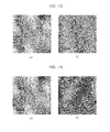
FIG. 15( a) is a Comparative Example showing an atomic force microscope (AFM) image of a GaN thin film grown without hollow structures, and FIG. 15( b) is an AFM image of a GaN thin film according to the present invention (Experimental Example 7). When comparing two images, it can be understood that defects such as dislocations or the like are greatly reduced in the case of the present invention, and surface condition of the GaN thin film is also very good.
Experimental Example 8
After growing the nitride thin film 815 like in the Experimental Example 6, a GaN thin film was additionally grown by increasing the reactor pressure to 300 torr.
FIG. 16( a) is a Comparative Example showing an atomic force microscope (AFM) image of a GaN thin film grown without hollow structures, and FIG. 16( b) is an AFM image of a GaN thin film according to the present invention (Experimental Example 8). When comparing two images, it can be understood that defects such as dislocations or the like are greatly reduced in the case of the present invention, and surface condition of the GaN thin film is also very good.
FIG. 17( a) is a Comparative Example showing the result of X-ray diffraction rocking curves (XRC) measured from a (002) plane of a GaN thin film grown without hollow structures, FIG. 17( b) is a Comparative Example showing the XRC result of a (102) plane of GaN grown without hollow structures, FIG. 17( c) is the XRC result of a (002) plane of GaN grown according to the present invention (Experimental Example 8), FIG. 17( d) is the XRC result of a (102) plane of GaN grown according to the present invention. When comparing the XRC results, it can be understood that crystallinity is also increased in the case of the present invention.
Although the nitride thin film structure and method of forming the same have been described with reference to the specific embodiments, they are not limited thereto. Therefore, it will be readily understood by those skilled in the art that various modifications and changes can be made thereto without departing from the spirit and scope of the present invention defined by the appended claims.

Claims (10)

The invention claimed is:
1. A semiconductor thin film structure, comprising:
a non-nitride substrate;
a plurality of particles coated on the substrate, wherein each particle comprises an inner cavity; and
a nitride thin film formed over the substrate by growing over the substrate exposed at a periphery of the particles to be combined over the particles,
wherein the substrate includes a material having a thermal expansion coefficient being larger than that of the nitride thin film, the particles are compressed by the nitride thin film and warpage of the substrate is prevented by the compressing of the particles during a cooling process after the forming of the nitride thin film.
2. The semiconductor thin film structure of claim 1, further comprising a buffer layer between the substrate and the nitride thin film.
3. The semiconductor thin film structure of claim 1 or 2, wherein the nitride thin film has two or more layers.
4. The semiconductor thin film structure of claim 3, further comprising a plurality of particles coated between two nitride thin film layers, wherein each of the particle which is coated between the two nitride thin film layers includes the inner cavity.
5. The semiconductor thin film structure of claim 4, wherein the particles formed closer to the substrate have larger size inner cavities than the particles formed farther away from the substrate.
6. The semiconductor thin film structure of claim 5, wherein each particle comprises a material having a refractive index different from that of the nitride thin film.
7. The semiconductor thin film structure of claim 4, wherein the particles formed closer to the substrate have larger coating density than the particles formed farther away from the substrate, when the size of the each particle is uniform.
8. The semiconductor thin film structure of claim 7, wherein the particles comprise a material having a refractive index different from that of the nitride thin film.
9. The semiconductor thin film structure of claim 1 or 2, wherein thermal expansion coefficient of the substrate is larger than that of the nitride thin film, and the particles are compressed by the nitride thin film.
10. A semiconductor device, comprising:
a non-nitride substrate;
a plurality of particles coated on the substrate, wherein each particle comprises an inner cavity; and
a semiconductor thin film structure comprising a nitride thin film formed over the substrate on which the particles are formed, by growing over the substrate exposed at a periphery of the particles to be combined over the particles,
wherein the substrate includes a material having a thermal expansion coefficient being larger than that of the nitride thin film, the particles are compressed by the nitride thin film and warpage of the substrate is prevented by the compressing of the particles during a cooling process after the forming of the nitride thin film.
US13/062,557 2008-09-08 2009-09-07 Structure of thin nitride film and formation method thereof Active 2030-01-03 US8847362B2 (en)

Applications Claiming Priority (5)

Application Number Priority Date Filing Date Title
KR10-2008-0088044 2008-09-08
KR20080088044 2008-09-08
KR10-2009-0083292 2009-09-04
KR1020090083292A KR101101780B1 (en) 2008-09-08 2009-09-04 Nitride thin film structure and method of forming the same
PCT/KR2009/005055 WO2010027230A2 (en) 2008-09-08 2009-09-07 Structure of thin nitride film and formation method thereof

Publications (2)

Publication Number Publication Date
US20110156214A1 US20110156214A1 (en) 2011-06-30
US8847362B2 true US8847362B2 (en) 2014-09-30

Family

ID=42179882

Family Applications (1)

Application Number Title Priority Date Filing Date
US13/062,557 Active 2030-01-03 US8847362B2 (en) 2008-09-08 2009-09-07 Structure of thin nitride film and formation method thereof

Country Status (6)

Country Link
US (1) US8847362B2 (en)
JP (1) JP5070359B2 (en)
KR (1) KR101101780B1 (en)
CN (1) CN102150286B (en)
DE (1) DE112009002065B4 (en)
WO (1) WO2010027230A2 (en)

Cited By (1)

* Cited by examiner, † Cited by third party
Publication number Priority date Publication date Assignee Title
US20150325741A1 (en) * 2013-08-21 2015-11-12 Sharp Kabushiki Kaisha Nitride semiconductor light emitting device

Families Citing this family (14)

* Cited by examiner, † Cited by third party
Publication number Priority date Publication date Assignee Title
KR101134191B1 (en) * 2010-04-26 2012-04-09 전북대학교산학협력단 Surface Plasmon Resonance-based Light Emitting Diode Using Core-Shell Nanoparticles
KR101810609B1 (en) * 2011-02-14 2017-12-20 삼성전자주식회사 Semiconductor device and method of manufacturing the same
KR101137514B1 (en) * 2011-03-11 2012-04-20 한국광기술원 Method for manufacturing nitride semiconductor device using nano particle
KR101235239B1 (en) * 2011-05-20 2013-02-21 서울대학교산학협력단 Semiconductor thin film structure and method of forming the same
KR101890751B1 (en) * 2012-09-05 2018-08-22 삼성전자주식회사 Nitride semiconductor device and method for fabricating the same
KR101420941B1 (en) * 2012-12-18 2014-07-21 한양대학교 산학협력단 GaN-based light emitting device with highly improved light extraction efficiency
CN103165779B (en) * 2013-02-08 2016-04-06 芜湖德豪润达光电科技有限公司 LED semiconductor element and manufacture method thereof
KR102099877B1 (en) * 2013-11-05 2020-04-10 삼성전자 주식회사 Method for fabricating nitride semiconductor device
KR101476098B1 (en) * 2014-04-22 2014-12-24 고려대학교 산학협력단 Method of inserting nano particles and manufacturing a photo functional layer using the same
KR20160008382A (en) * 2014-07-14 2016-01-22 서울대학교산학협력단 Semiconductor thin film structure, method and apparatus for separating nitride semiconductor using the same
KR101636140B1 (en) * 2014-08-22 2016-07-07 한양대학교 산학협력단 Light emitting device, and method of fabricating the same
JP2018113386A (en) * 2017-01-13 2018-07-19 株式会社ディスコ Method for manufacturing light-emitting diode chip and light-emitting diode chip
US10373825B1 (en) 2018-05-29 2019-08-06 Industry-University Cooperation Foundation Hanyang University Method for manufacturing gallium nitride substrate using core-shell nanoparticle
WO2023076607A1 (en) * 2021-10-29 2023-05-04 The Regents Of The University Of California Light emitting diodes containing epitaxial light control features

Citations (10)

* Cited by examiner, † Cited by third party
Publication number Priority date Publication date Assignee Title
CN1413357A (en) 1999-12-24 2003-04-23 丰田合成株式会社 Method for producing group III nitride compound semiconductor and group III nitride compound semiconductor device
US20050077512A1 (en) 2003-10-13 2005-04-14 Samsung Electro-Mechanics Co., Ltd. Nitride semiconductors on silicon substrate and method of manufacturing the same
CN1745468A (en) 2002-09-30 2006-03-08 纳米系统公司 Large-area nanoenabled macroelectronic substrates and uses therefor
US20060216849A1 (en) 2003-05-30 2006-09-28 S.O.I.Tec Silicon On Insulator Technologies S.A. Substrate for stressed systems and method of making same
KR100638880B1 (en) 2005-08-18 2006-10-27 삼성전기주식회사 Semiconductor laminated structure and method of manufacturing nitride semiconductor crystal substrate and nitride semiconductor device
US20060270201A1 (en) 2005-05-13 2006-11-30 Chua Soo J Nano-air-bridged lateral overgrowth of GaN semiconductor layer
US20060278880A1 (en) * 2005-06-10 2006-12-14 Arima Computer Corporation Light emitting semiconductor device
US20070072396A1 (en) 2003-09-26 2007-03-29 Centre National De La Recherche Scientifique(Cnrs) Method of producing self supporting substrates comprising iii-nitrides by means of heteroepitaxy on a sacrificial layer
US20080050599A1 (en) 2001-01-18 2008-02-28 Sony Corporation Crystal film, crystal substrate, and semiconductor device
US20090111250A1 (en) * 2007-10-24 2009-04-30 Ho-Jun Lee Method for preparing compound semiconductor substrate

Family Cites Families (5)

* Cited by examiner, † Cited by third party
Publication number Priority date Publication date Assignee Title
JP4882351B2 (en) * 2004-11-24 2012-02-22 住友化学株式会社 Semiconductor laminated substrate, manufacturing method thereof, and light emitting device
KR100712753B1 (en) * 2005-03-09 2007-04-30 주식회사 실트론 Compound semiconductor device and method for manufacturing the same
JP2006278512A (en) * 2005-03-28 2006-10-12 Fujitsu Ltd Insulating film and its manufacturing method, and electronic device
JPWO2007145088A1 (en) * 2006-06-14 2009-10-29 コニカミノルタエムジー株式会社 Semiconductor nanoparticles and manufacturing method thereof
GB0701069D0 (en) * 2007-01-19 2007-02-28 Univ Bath Nanostructure template and production of semiconductors using the template

Patent Citations (13)

* Cited by examiner, † Cited by third party
Publication number Priority date Publication date Assignee Title
CN1413357A (en) 1999-12-24 2003-04-23 丰田合成株式会社 Method for producing group III nitride compound semiconductor and group III nitride compound semiconductor device
US20080050599A1 (en) 2001-01-18 2008-02-28 Sony Corporation Crystal film, crystal substrate, and semiconductor device
CN1745468A (en) 2002-09-30 2006-03-08 纳米系统公司 Large-area nanoenabled macroelectronic substrates and uses therefor
US20060216849A1 (en) 2003-05-30 2006-09-28 S.O.I.Tec Silicon On Insulator Technologies S.A. Substrate for stressed systems and method of making same
US20070072396A1 (en) 2003-09-26 2007-03-29 Centre National De La Recherche Scientifique(Cnrs) Method of producing self supporting substrates comprising iii-nitrides by means of heteroepitaxy on a sacrificial layer
US20050077512A1 (en) 2003-10-13 2005-04-14 Samsung Electro-Mechanics Co., Ltd. Nitride semiconductors on silicon substrate and method of manufacturing the same
CN1607683A (en) 2003-10-13 2005-04-20 三星电机株式会社 Nitride semiconductors on silicon substrate and method of manufacturing the same
KR100744933B1 (en) 2003-10-13 2007-08-01 삼성전기주식회사 Nitride Semiconductors on Silicon Substrate and Manufacturing Method thereof
US20060270201A1 (en) 2005-05-13 2006-11-30 Chua Soo J Nano-air-bridged lateral overgrowth of GaN semiconductor layer
US20060278880A1 (en) * 2005-06-10 2006-12-14 Arima Computer Corporation Light emitting semiconductor device
US20070141741A1 (en) 2005-08-18 2007-06-21 Samsung Electro-Mechanics Co., Ltd. Semiconductor laminated structure and method of manufacturing nitirde semiconductor crystal substrate and nitirde semiconductor device
KR100638880B1 (en) 2005-08-18 2006-10-27 삼성전기주식회사 Semiconductor laminated structure and method of manufacturing nitride semiconductor crystal substrate and nitride semiconductor device
US20090111250A1 (en) * 2007-10-24 2009-04-30 Ho-Jun Lee Method for preparing compound semiconductor substrate

Non-Patent Citations (1)

* Cited by examiner, † Cited by third party
Title
Wang-Nang Wang, GaN epitaxial layer over growth method, Aug. 13, 2008.

Cited By (1)

* Cited by examiner, † Cited by third party
Publication number Priority date Publication date Assignee Title
US20150325741A1 (en) * 2013-08-21 2015-11-12 Sharp Kabushiki Kaisha Nitride semiconductor light emitting device

Also Published As

Publication number Publication date
JP5070359B2 (en) 2012-11-14
US20110156214A1 (en) 2011-06-30
JP2012502461A (en) 2012-01-26
WO2010027230A2 (en) 2010-03-11
DE112009002065T5 (en) 2011-07-14
DE112009002065B4 (en) 2017-04-20
CN102150286A (en) 2011-08-10
WO2010027230A3 (en) 2010-07-08
KR101101780B1 (en) 2012-01-05
KR20100029704A (en) 2010-03-17
CN102150286B (en) 2015-09-23

Similar Documents

Publication Publication Date Title
US8847362B2 (en) Structure of thin nitride film and formation method thereof
KR101038069B1 (en) Method of zinc oxide film grown on the epitaxial lateral overgrowth gallium nitride template
JP4901145B2 (en) Compound semiconductor device and manufacturing method thereof
JP5838523B2 (en) Semipolar (Al, In, Ga, B) N or Group III nitride crystals
US9741560B2 (en) Method of growing nitride semiconductor layer
KR100994643B1 (en) Manufacturing method of compound semiconductor substrate using spherical balls, compound semiconductor substrate and compound semiconductor device using the same
US20130168833A1 (en) METHOD FOR ENHANCING GROWTH OF SEMIPOLAR (Al,In,Ga,B)N VIA METALORGANIC CHEMICAL VAPOR DEPOSITION
TWI521733B (en) Method for producing ga-containing group iii nitride semiconductor
US20130260495A1 (en) Light emitting devices and methods of manufacturing the same
JP2006523033A (en) Method for growing single crystal GaN on silicon
TW201540861A (en) Method of growing Group-III nitride semiconductor and method of forming nitride crystal on substrate
JP2012209586A (en) Device structure having semipolar nitride, and characterized in nitride nucleation layer or buffer layer
US6648966B2 (en) Wafer produced thereby, and associated methods and devices using the wafer
JP6165884B2 (en) Semiconductor laminate and method for producing semiconductor laminate
KR100533636B1 (en) Fabrication method of nitride semiconductor and nitride semiconductor structure fabricated thereby
US20150087137A1 (en) Nitride thin film stucture and method of forming the same
KR20100104997A (en) Nitride semiconductor substrate having dislocation blocking layer and manufacturing method thereof
JP2002299267A (en) Manufacturing method for semiconductor wafer
KR101466037B1 (en) Substrate for semiconductor device, nitride thin film structure using the same and method of forming the same
CN114267758B (en) Light-emitting diode epitaxial wafer and preparation method thereof
KR101020498B1 (en) Method for epitaxial growth
KR101919353B1 (en) Nitride-based semiconductor nano rod and manufacturing method of the same
EP1898449B1 (en) Compound semiconductor devices and methods of manufacturing the same
TW201513176A (en) A semiconductor wafer and a method for producing the semiconductor wafer
KR100839224B1 (en) Method for manufacturing thick film of gan

Legal Events

Date Code Title Description
AS Assignment

Owner name: SNU R&DB FOUNDATION, KOREA, REPUBLIC OF

Free format text: ASSIGNMENT OF ASSIGNORS INTEREST;ASSIGNORS:YOON, EUIJOON;CHAR, KOOKHEON;KIM, JONG HAK;AND OTHERS;REEL/FRAME:025909/0094

Effective date: 20110222

STCF Information on status: patent grant

Free format text: PATENTED CASE

AS Assignment

Owner name: SEOUL TECHNO HOLDING, INC., KOREA, REPUBLIC OF

Free format text: ASSIGNMENT OF ASSIGNORS INTEREST;ASSIGNOR:SNU R&DB FOUNDATION;REEL/FRAME:035523/0745

Effective date: 20150302

Owner name: HEXASOLUTION CO., LTD., KOREA, REPUBLIC OF

Free format text: ASSIGNMENT OF ASSIGNORS INTEREST;ASSIGNOR:SEOUL TECHNO HOLDING, INC.;REEL/FRAME:035524/0425

Effective date: 20150316

MAFP Maintenance fee payment

Free format text: PAYMENT OF MAINTENANCE FEE, 4TH YR, SMALL ENTITY (ORIGINAL EVENT CODE: M2551)

Year of fee payment: 4

MAFP Maintenance fee payment

Free format text: PAYMENT OF MAINTENANCE FEE, 8TH YR, SMALL ENTITY (ORIGINAL EVENT CODE: M2552); ENTITY STATUS OF PATENT OWNER: SMALL ENTITY

Year of fee payment: 8