US8852969B2 - Fabrication of compact opto-electronic component packages - Google Patents
Fabrication of compact opto-electronic component packages Download PDFInfo
- Publication number
- US8852969B2 US8852969B2 US12/938,512 US93851210A US8852969B2 US 8852969 B2 US8852969 B2 US 8852969B2 US 93851210 A US93851210 A US 93851210A US 8852969 B2 US8852969 B2 US 8852969B2
- Authority
- US
- United States
- Prior art keywords
- semiconductor wafer
- opto
- electronic component
- metallization
- vias
- Prior art date
- Legal status (The legal status is an assumption and is not a legal conclusion. Google has not performed a legal analysis and makes no representation as to the accuracy of the status listed.)
- Expired - Fee Related, expires
Links
Images


Classifications
-
- H—ELECTRICITY
- H01—ELECTRIC ELEMENTS
- H01L—SEMICONDUCTOR DEVICES NOT COVERED BY CLASS H10
- H01L33/00—Semiconductor devices with at least one potential-jump barrier or surface barrier specially adapted for light emission; Processes or apparatus specially adapted for the manufacture or treatment thereof or of parts thereof; Details thereof
- H01L33/48—Semiconductor devices with at least one potential-jump barrier or surface barrier specially adapted for light emission; Processes or apparatus specially adapted for the manufacture or treatment thereof or of parts thereof; Details thereof characterised by the semiconductor body packages
- H01L33/62—Arrangements for conducting electric current to or from the semiconductor body, e.g. lead-frames, wire-bonds or solder balls
-
- H—ELECTRICITY
- H01—ELECTRIC ELEMENTS
- H01L—SEMICONDUCTOR DEVICES NOT COVERED BY CLASS H10
- H01L21/00—Processes or apparatus adapted for the manufacture or treatment of semiconductor or solid state devices or of parts thereof
- H01L21/70—Manufacture or treatment of devices consisting of a plurality of solid state components formed in or on a common substrate or of parts thereof; Manufacture of integrated circuit devices or of parts thereof
- H01L21/71—Manufacture of specific parts of devices defined in group H01L21/70
- H01L21/768—Applying interconnections to be used for carrying current between separate components within a device comprising conductors and dielectrics
- H01L21/76898—Applying interconnections to be used for carrying current between separate components within a device comprising conductors and dielectrics formed through a semiconductor substrate
-
- H—ELECTRICITY
- H01—ELECTRIC ELEMENTS
- H01L—SEMICONDUCTOR DEVICES NOT COVERED BY CLASS H10
- H01L23/00—Details of semiconductor or other solid state devices
- H01L23/48—Arrangements for conducting electric current to or from the solid state body in operation, e.g. leads, terminal arrangements ; Selection of materials therefor
- H01L23/481—Internal lead connections, e.g. via connections, feedthrough structures
-
- H—ELECTRICITY
- H01—ELECTRIC ELEMENTS
- H01L—SEMICONDUCTOR DEVICES NOT COVERED BY CLASS H10
- H01L2224/00—Indexing scheme for arrangements for connecting or disconnecting semiconductor or solid-state bodies and methods related thereto as covered by H01L24/00
- H01L2224/01—Means for bonding being attached to, or being formed on, the surface to be connected, e.g. chip-to-package, die-attach, "first-level" interconnects; Manufacturing methods related thereto
- H01L2224/42—Wire connectors; Manufacturing methods related thereto
- H01L2224/47—Structure, shape, material or disposition of the wire connectors after the connecting process
- H01L2224/48—Structure, shape, material or disposition of the wire connectors after the connecting process of an individual wire connector
- H01L2224/4805—Shape
- H01L2224/4809—Loop shape
- H01L2224/48091—Arched
-
- H—ELECTRICITY
- H01—ELECTRIC ELEMENTS
- H01L—SEMICONDUCTOR DEVICES NOT COVERED BY CLASS H10
- H01L2224/00—Indexing scheme for arrangements for connecting or disconnecting semiconductor or solid-state bodies and methods related thereto as covered by H01L24/00
- H01L2224/01—Means for bonding being attached to, or being formed on, the surface to be connected, e.g. chip-to-package, die-attach, "first-level" interconnects; Manufacturing methods related thereto
- H01L2224/42—Wire connectors; Manufacturing methods related thereto
- H01L2224/47—Structure, shape, material or disposition of the wire connectors after the connecting process
- H01L2224/48—Structure, shape, material or disposition of the wire connectors after the connecting process of an individual wire connector
- H01L2224/481—Disposition
- H01L2224/48151—Connecting between a semiconductor or solid-state body and an item not being a semiconductor or solid-state body, e.g. chip-to-substrate, chip-to-passive
- H01L2224/48221—Connecting between a semiconductor or solid-state body and an item not being a semiconductor or solid-state body, e.g. chip-to-substrate, chip-to-passive the body and the item being stacked
- H01L2224/48225—Connecting between a semiconductor or solid-state body and an item not being a semiconductor or solid-state body, e.g. chip-to-substrate, chip-to-passive the body and the item being stacked the item being non-metallic, e.g. insulating substrate with or without metallisation
- H01L2224/48227—Connecting between a semiconductor or solid-state body and an item not being a semiconductor or solid-state body, e.g. chip-to-substrate, chip-to-passive the body and the item being stacked the item being non-metallic, e.g. insulating substrate with or without metallisation connecting the wire to a bond pad of the item
-
- H—ELECTRICITY
- H01—ELECTRIC ELEMENTS
- H01L—SEMICONDUCTOR DEVICES NOT COVERED BY CLASS H10
- H01L2224/00—Indexing scheme for arrangements for connecting or disconnecting semiconductor or solid-state bodies and methods related thereto as covered by H01L24/00
- H01L2224/01—Means for bonding being attached to, or being formed on, the surface to be connected, e.g. chip-to-package, die-attach, "first-level" interconnects; Manufacturing methods related thereto
- H01L2224/42—Wire connectors; Manufacturing methods related thereto
- H01L2224/47—Structure, shape, material or disposition of the wire connectors after the connecting process
- H01L2224/48—Structure, shape, material or disposition of the wire connectors after the connecting process of an individual wire connector
- H01L2224/484—Connecting portions
- H01L2224/48463—Connecting portions the connecting portion on the bonding area of the semiconductor or solid-state body being a ball bond
- H01L2224/48465—Connecting portions the connecting portion on the bonding area of the semiconductor or solid-state body being a ball bond the other connecting portion not on the bonding area being a wedge bond, i.e. ball-to-wedge, regular stitch
-
- H—ELECTRICITY
- H01—ELECTRIC ELEMENTS
- H01L—SEMICONDUCTOR DEVICES NOT COVERED BY CLASS H10
- H01L2224/00—Indexing scheme for arrangements for connecting or disconnecting semiconductor or solid-state bodies and methods related thereto as covered by H01L24/00
- H01L2224/73—Means for bonding being of different types provided for in two or more of groups H01L2224/10, H01L2224/18, H01L2224/26, H01L2224/34, H01L2224/42, H01L2224/50, H01L2224/63, H01L2224/71
- H01L2224/732—Location after the connecting process
- H01L2224/73251—Location after the connecting process on different surfaces
- H01L2224/73265—Layer and wire connectors
-
- H—ELECTRICITY
- H01—ELECTRIC ELEMENTS
- H01L—SEMICONDUCTOR DEVICES NOT COVERED BY CLASS H10
- H01L24/00—Arrangements for connecting or disconnecting semiconductor or solid-state bodies; Methods or apparatus related thereto
- H01L24/01—Means for bonding being attached to, or being formed on, the surface to be connected, e.g. chip-to-package, die-attach, "first-level" interconnects; Manufacturing methods related thereto
- H01L24/42—Wire connectors; Manufacturing methods related thereto
- H01L24/47—Structure, shape, material or disposition of the wire connectors after the connecting process
- H01L24/48—Structure, shape, material or disposition of the wire connectors after the connecting process of an individual wire connector
-
- H—ELECTRICITY
- H01—ELECTRIC ELEMENTS
- H01L—SEMICONDUCTOR DEVICES NOT COVERED BY CLASS H10
- H01L2924/00—Indexing scheme for arrangements or methods for connecting or disconnecting semiconductor or solid-state bodies as covered by H01L24/00
- H01L2924/0001—Technical content checked by a classifier
- H01L2924/00014—Technical content checked by a classifier the subject-matter covered by the group, the symbol of which is combined with the symbol of this group, being disclosed without further technical details
-
- H—ELECTRICITY
- H01—ELECTRIC ELEMENTS
- H01L—SEMICONDUCTOR DEVICES NOT COVERED BY CLASS H10
- H01L2924/00—Indexing scheme for arrangements or methods for connecting or disconnecting semiconductor or solid-state bodies as covered by H01L24/00
- H01L2924/01—Chemical elements
- H01L2924/01019—Potassium [K]
-
- H—ELECTRICITY
- H01—ELECTRIC ELEMENTS
- H01L—SEMICONDUCTOR DEVICES NOT COVERED BY CLASS H10
- H01L2924/00—Indexing scheme for arrangements or methods for connecting or disconnecting semiconductor or solid-state bodies as covered by H01L24/00
- H01L2924/10—Details of semiconductor or other solid state devices to be connected
- H01L2924/102—Material of the semiconductor or solid state bodies
- H01L2924/1025—Semiconducting materials
- H01L2924/10251—Elemental semiconductors, i.e. Group IV
- H01L2924/10253—Silicon [Si]
-
- H—ELECTRICITY
- H01—ELECTRIC ELEMENTS
- H01L—SEMICONDUCTOR DEVICES NOT COVERED BY CLASS H10
- H01L2924/00—Indexing scheme for arrangements or methods for connecting or disconnecting semiconductor or solid-state bodies as covered by H01L24/00
- H01L2924/10—Details of semiconductor or other solid state devices to be connected
- H01L2924/11—Device type
- H01L2924/12—Passive devices, e.g. 2 terminal devices
- H01L2924/1204—Optical Diode
- H01L2924/12041—LED
-
- H—ELECTRICITY
- H01—ELECTRIC ELEMENTS
- H01L—SEMICONDUCTOR DEVICES NOT COVERED BY CLASS H10
- H01L2924/00—Indexing scheme for arrangements or methods for connecting or disconnecting semiconductor or solid-state bodies as covered by H01L24/00
- H01L2924/10—Details of semiconductor or other solid state devices to be connected
- H01L2924/11—Device type
- H01L2924/14—Integrated circuits
-
- H—ELECTRICITY
- H01—ELECTRIC ELEMENTS
- H01L—SEMICONDUCTOR DEVICES NOT COVERED BY CLASS H10
- H01L2924/00—Indexing scheme for arrangements or methods for connecting or disconnecting semiconductor or solid-state bodies as covered by H01L24/00
- H01L2924/15—Details of package parts other than the semiconductor or other solid state devices to be connected
- H01L2924/181—Encapsulation
-
- H—ELECTRICITY
- H01—ELECTRIC ELEMENTS
- H01L—SEMICONDUCTOR DEVICES NOT COVERED BY CLASS H10
- H01L2924/00—Indexing scheme for arrangements or methods for connecting or disconnecting semiconductor or solid-state bodies as covered by H01L24/00
- H01L2924/30—Technical effects
- H01L2924/301—Electrical effects
- H01L2924/3025—Electromagnetic shielding
-
- H—ELECTRICITY
- H01—ELECTRIC ELEMENTS
- H01L—SEMICONDUCTOR DEVICES NOT COVERED BY CLASS H10
- H01L2933/00—Details relating to devices covered by the group H01L33/00 but not provided for in its subgroups
- H01L2933/0008—Processes
- H01L2933/0016—Processes relating to electrodes
-
- H—ELECTRICITY
- H01—ELECTRIC ELEMENTS
- H01L—SEMICONDUCTOR DEVICES NOT COVERED BY CLASS H10
- H01L33/00—Semiconductor devices with at least one potential-jump barrier or surface barrier specially adapted for light emission; Processes or apparatus specially adapted for the manufacture or treatment thereof or of parts thereof; Details thereof
- H01L33/48—Semiconductor devices with at least one potential-jump barrier or surface barrier specially adapted for light emission; Processes or apparatus specially adapted for the manufacture or treatment thereof or of parts thereof; Details thereof characterised by the semiconductor body packages
- H01L33/483—Containers
- H01L33/486—Containers adapted for surface mounting
Definitions
- This invention relates to opto-electronic component packages.
- LEDs light emitting diodes
- Ceramics such as alumina oxide (Al 2 O 3 ) or aluminum nitride (AIN) are used in the packaging of high brightness LEDs.
- PLCC plastic leadless chip carriers
- PLCC plastic leadless chip carriers
- These types of packages often have large footprints, poor thermal conductivity and large mechanical tolerances and are not flexible to design changes, thus making application-specific designs difficult.
- PCB printed circuit board
- the height of an assembled PCB (e.g., the circuit elements mounted on both sides of the PCB) is limited to be about one millimeter (mm), whereas the typical height of the assembled PCB is 1.5 mm (a typical height of a PCB is 500 microns ( ⁇ m) and a typical height of circuit elements is 500 ⁇ m). Therefore, either the size of the assembled PCB must be reduced or features and capabilities must be reduced to fit the assembled PCB into the limited available space. In addition, thermal performance of the circuit elements is also a consideration.
- the packages can be fabricated, for example, in a wafer-level batch process.
- Fabrication techniques are disclosed for an opto-electronic component package in which the opto-electronic component is mounted to a semiconductor wafer having first and second surfaces on opposite sides of the wafer.
- the first surface includes anode and cathode contact pads electrically connected to the opto-electronic component which is mounted to the side of the semiconductor wafer having the second surface.
- the method includes etching vias in the first surface of the semiconductor wafer.
- the vias extend partially through the semiconductor wafer.
- Metal is provided on the first surface of the semiconductor wafer and surfaces in the vias.
- the metal is structured to define a thermal pad for heat transfer away from the opto-electronic component and to define the anode and cathode contact pads electrically connected to metallization in the vias.
- a carrier wafer is attached on the side of the semiconductor wafer having the first surface, and the semiconductor wafer is thinned from its second surface to expose the metallization in the vias.
- Metal is provided on the second surface of the semiconductor wafer and structured to define a die attach pad and to define additional anode and cathode pads for the opto-electronic component.
- the additional anode and cathode pads are electrically connected to metallization in the vias, and the opto-electronic component is mounted on the die attach pad.
- a protective cover that is transparent to a wavelength of light emitted by or received by the opto-electronic component is formed over the opto-electronic component.
- Some implementations result in smaller or thinner packages that provide better thermal isolation or performance and can provide for greater design flexibility which allows for changes to the design to be easily incorporated into a manufacturing process.
- various modifications to the process can be made such that the process can be used with a LED or other opto-electronic component package with an integrated electronic circuit structure.
- FIG. 1 a is an example of a LED package.
- FIG. 1 b is a second example of a LED package.
- FIG. 1 c is a third example of a LED package.
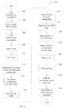
- FIG. 2 is a flowchart illustrating an example of a process to form a thin LED package.
- FIG. 3 is an illustration of a semiconductor wafer.
- FIG. 4 is an illustration of a base.
- FIG. 5 is an illustration of a base with vias.
- FIG. 6 is an illustration of the SMD side of the base after a metallization process.
- FIG. 7 is an illustration of the LED side of the base after a carrier wafer has been attached.
- FIG. 8 is an illustration of the LED side of the base after a metallization process.
- FIG. 9 is a flowchart illustrating an example of a process to form a thin LED package with an integrated electronic circuit structure.
- FIG. 10 is an illustration of a electronic circuit structure bonded to a base.
- FIG. 11 is an illustration of a electronic circuit structure after predetermined portions of the electronic circuit structure have been removed.
- FIG. 12 is an illustration of an electronic circuit structure after undergoing a passivation process.
- FIG. 13 is an illustration of a base after the vias are formed by an etching process.
- FIG. 14 is an illustration of a carrier wafer bonded to the electronic circuit structure.
- FIG. 15 is an illustration of base with the exposed feed-through metallization.
- FIG. 16 is an illustration of the thin LED package with an integrated electronic circuit structure after a thermal pad and wirebonding pads have been formed.
- FIG. 17 is an illustration of an SMD side of the thin LED package with an integrated electronic circuit structure.
- FIGS. 1 a and 1 b illustrate examples of thin LED packages 100 and 150 with enhanced thermal performance 100 and 150 .
- FIGS. 1 a and 1 b are described with respect to a LED 108
- the LED 108 can be replaced with other types of opto-electronic components.
- the LED 108 is replaced by an infra-red emitter (e.g., a vertical-cavity surface-emitting laser), an infra-red receiver (e.g., a pin diode) or an infra-red transceiver.
- the fabrication processes described below can be used to make packages for opto-electronic components other than LEDs.
- the LED package 100 includes a base 102 , a reflector 104 , feed-through metallization 106 , a reflective surface 107 , an LED 108 , a LED die attach pad 110 a (located underneath the LED 108 ) and wirebond pads 110 b .
- the base 102 is formed from a silicon or other semiconductor wafer.
- the physical dimensions (e.g., the height 112 , the width 114 and the depth 116 ) of the LED package 100 may vary depending on the size of the LED, the application, or the intended use of the LED package.
- An example package 100 has a height 112 equal to about 550 ⁇ m, a width 114 equal to about 3100 ⁇ m and a depth 116 equal to about 3100 ⁇ m.
- the height 112 includes the height of the reflector 104 and the height of the base 102 .
- the height of the reflector 104 can be 400 ⁇ m and the height of the base 102 can be 150 ⁇ m.
- the physical dimensions can be increased or decreased to accommodate different size opto-electronic components 108 or based on the intended use of the LED package 100 .
- the base 102 can have a height from 100 ⁇ m to 400 ⁇ m.
- the base 102 contains one or more vias with feed-through metallization 106 that extends from the surface-mount-device (SMD) side 118 of the base (i.e., the side of the base 102 that is to be mounted to a PCB).
- the feed-through metallization 106 in each of the vias protrudes from the LED side 119 of the base (i.e., the side of the base 102 that the LED 108 is mounted to and opposite the SMD side 118 ) and is used to form electrical interconnections between the PCB and the LED package 100 .
- the number of vias with feed-through metallization 106 is typically two, but can be increased depending on the number of LEDs 108 that are mounted on the base 102 . For example, an array of LEDS 108 may be placed on the base 102 .
- the base 102 includes the reflective surface 107 , which can be a thin layer of metal such as aluminum, silver, or some other reflective material.
- FIG. 1 a illustrates the LED package 100 with a single circular reflective surface 107
- the base 102 can have multiple reflective surfaces 107 and is not limited to circular geometries.
- FIG. 1 b illustrates a rectangular reflective surface 107 .
- the reflective surface 107 enables enhanced light output efficiency and helps direct the light out of the LED package.
- the reflector 104 can be used to increase the light directed out of the LED package 100 .
- the reflector 104 can be, for example, a plastic molded structure with round parabolic walls or vertical walls.
- the reflector 104 can have different geometries depending on the application of the LED package 100 .
- the reflector 104 has a round parabolic wall as illustrated in FIG. 1 a .
- the slope of the parabolic wall can be 45 degrees or any other angle depending on the application of the LED package 100 .
- the reflector 104 does not have a parabolic wall.
- FIG. 1 b illustrates a reflector 104 with vertical walls, sometimes referred to as a cavity substrate.
- the reflector 104 also can be used as a stand-off for optical components.
- a lens for beam shaping can be mounted to the top of the reflector 104 .
- the LED packages 100 and 150 both include a reflector 104 , in some implementations, the reflector 104 is omitted.
- FIG. 1 c is an example LED package 190 where the reflector 104 is omitted.
- the LED package 190 includes a lens 192 that is attached to the LED side 119 of the base and covers the LED 108 .
- the lens 192 can be used to focus the light emitted from the LED package 190 or to enhance the light output of the LED package 190 .
- the LED 108 is mounted to the base 102 by the LED die attach pad 110 a located underneath the LED 108 .
- the LED die attach pad 110 a is formed on the LED side 119 of the base and can be connected to electrical ground.
- the LED 108 also can be electrically connected to the wirebond pads 110 b , also referred to as anode and cathode pads.
- anode and cathode pads 110 b are provided near the die attach pads 110 a .
- the die attach pad 110 a can act as the electrical ground electrode and the wirebond pads 110 b form a contact only to the cathode of the LED 108 .
- FIG. 2 is a flowchart illustrating a wafer-level process 200 to form the LED package 100 or 150 .
- the process 200 is typically performed on a silicon or other semiconductor wafer to define multiple bases 102 for individual, discrete packages.
- An example of a semiconductor wafer 175 with areas defining multiple bases 102 is shown in FIG. 3 .
- the fabrication process can be performed at the wafer level, for ease of discussion and illustration, the individual steps of process 200 are described below as being performed with respect to a section of the semiconductor wafer 175 defining a single base 102 .
- the process 200 begins with a silicon or other semiconductor wafer having a thickness, for example, of 650 ⁇ m.
- FIG. 4 illustrates a section of the wafer 175 defining a single base 102 before any processing has occurred.
- a dielectric mask such as silicon dioxide (SiO 2 ) or silicon nitride (Si x /N y ), is grown on the base 102 (block 202 ).
- the vias then are etched into the SMD side 118 of the base (block 204 ).
- the vias 122 can be etched using a wet etching technique such as potassium hydroxide (KOH) etching or tetramethyl ammonium hydroxide (TMAH) etching.
- KOH potassium hydroxide
- TMAH tetramethyl ammonium hydroxide
- the vias 122 can be etched using a dry etching technique.
- the vias 122 can be etched to any desired depth, so long as they do not penetrate the bottom of the base 102 (i.e., the vias 122 remain buried).
- FIG. 5 illustrates the base 102 after the vias 122 are etched.
- the SMD side 118 of the base and the vias 122 then undergo an oxidation process.
- SiO 2 can be grown on the SMD side 118 , in the vias 122 and on the LED side 119 of the base.
- the SMD side 118 of the base and the vias 122 undergo a metallization process that forms the feed-through metallization 106 (block 206 ).
- the feed-through metallization 106 can be formed, for example, by the deposition of conductive metals in the vias 122 .
- Metals such as chromium, titanium, gold, copper, nickel, aluminum, and silver are deposited on predetermined portions of the SMD side 118 of the base and the vias 122 , and one or more layers of metals can be deposited (i.e., a metal stack).
- metal is deposited on the entire surface of the SMD side 118 of the base and in the vias 122 .
- metal can be selectively deposited in the vias 122 and in areas around the corners of the SMD side 118 of the base.
- the SMD side 118 of the base then is processed (i.e., structured) to create a thermal pad 124 and electrical contact pads 126 (block 208 ).
- the SMD side 118 is processed by removing predetermined portions of the metal deposited on the SMD side 118 .
- the metal can be selectively removed to form the thermal pad 124 and the contact pads 126 by applying a mask and using a known etching technique. For example, a wet etching technique or a dry etching technique can be used.
- the thermal pad 124 is electrically insulated from the electrical contact pads 126 .
- the thermal pad 124 allows for efficient heat transfer from the LED 108 to the surface on which the package 100 is mounted (e.g., a PCB).
- the contact pads 126 serve as anode or cathode contact pads that allow the LED package 100 to make electrical connections through the feed-through metallization to the PCB.
- FIG. 6 is an illustration of the SMD side 118 of the base after it has been structured and the thermal pad 124 and the electrical contact pads 126 have been formed. Although FIG. 6 illustrates a single thermal pad 124 , the SMD side 118 of the base can include multiple thermal pads 124 . For example, if multiple LEDs or an array of LEDs are contained in the package, then the SMD side 118 of the base can include multiple thermal pads 124 .
- the SMD side 118 of the base can be processed to form solder dams 128 in the areas around the feed-through metallization 106 .
- the solder dams 128 can be formed by depositing a mask on the SMD side 118 of the base and selectively removing portions of the metal stack to expose a layer of the metal stack that is not wetable by solder.
- metal can be removed to expose a layer of titanium. The solder dams 128 prevent solder from flowing from the electrical contact pads 126 into the feed-through metallization 106 .
- a carrier wafer 130 then is bonded to the SMD side 118 of the wafer being provided (block 210 ).
- the carrier wafer 130 can be, for example, a silicon wafer, a glass wafer, or a wafer of some other material.
- the carrier wafer 130 can be bonded to the base 102 , for example, with an adhesive bonding process or some other type of non-permanent bonding process.
- the LED side 119 of the base is processed to expose the feed-through metallization 106 in the vias 122 (block 212 ).
- a mechanical grinding technique can be used to reduce the thickness of the base 102 from the LED side 119 of the base 102 .
- the base 102 is supported by the carrier wafer 130 for mechanical stability during the grinding process and subsequent processing steps.
- the base 102 is thinned until its thickness is approximately 210 ⁇ m.
- the LED side 119 of the base 102 then is dry-etched to open the feed-through metallization 106 .
- the base 102 can be dry-etched using a reactive ion etching (RIE) process.
- RIE reactive ion etching
- the RIE process removes approximately 60 ⁇ m to open the feed-through metallization 106 .
- the material of the base 102 is removed at a faster rate than the dielectric coating of the vias 122 . As shown in FIG. 7 , this difference in etching rates results in the feed-through metallization 106 being exposed and protruding slightly beyond the SMD side 118 of the base.
- a dielectric mask is then deposited on the SMD side 118 of the base to provide electrical insulation (block 213 ).
- the dielectric mask can be deposited by a plasma-enhanced chemical vapor deposition (PE-CVD) process.
- PE-CVD plasma-enhanced chemical vapor deposition
- the feed-through metallization 106 is then opened by removing the dielectric coating from the feed-through metallization 106 .
- the dielectric coating can be removed by applying a mask such as a photoresist and etching the dielectric coating covering the feed-through metallization 106 .
- a wet etching technique or a dry etching technique can be used. Other techniques to expose the feed-through metallization may be used.
- Metal is then deposited on the LED side 119 of the base 102 (block 214 ) to form electrical connections with the feed-through metallization 106 and the anode and cathode pads 110 b and the reflective surface 107 .
- the anode and cathode pads 110 b and the reflective surface 107 can be formed by applying a photoresist mask and using a wet or dry etching process.
- a metal such as titanium, chromium, aluminum, nickel, copper, silver, gold or some combination of these metals can be used to form the LED die attach pad 110 a , the pads 110 b and the reflective surface 107 .
- the amount and thickness of the metal deposited varies with the type of metal deposited.
- titanium is used as the metal and is deposited so that the titanium layer has a thickness of about 100 nm.
- gold is used as the metal and is deposited so that the thickness of the gold layer is approximately 1000 nm.
- the metal can be deposited using a thin film metallization process such as a sputter deposition process and using a gold finish for the LED die attach pad 110 a and the wirebond pads 110 b .
- the metals can be deposited using electroplating techniques.
- the metal can be selectively removed by applying a mask and using known wet or dry etching techniques.
- the anode and cathode pads 110 b can be electrically connected to the feed-through metallization 106 .
- FIG. 8 is an illustration of the SMD side 118 of the base after the LED die attach pad 110 a , the pads 110 b and the reflective surface 107 are formed.
- the reflector 104 is aligned on the LED side of the base 102 and then attached to the base 102 (block 216 ).
- the reflector 104 may be attached to the base 102 , for example, using an adhesive bonding process or by transfer or compression molding.
- the reflector 104 is positioned on the base 102 so that the reflective surface 107 , the LED die attach pad 110 a and the pad 110 b are within the cavity defined by the reflector 104 .
- a cavity substrate is attached instead of a reflector with round parabolic walls.
- the cavity substrate can be made from a polymer and attached to base 102 , for example, using an adhesive bonding process or by transfer or compression molding.
- the carrier wafer 130 is removed from the SMD side 118 of the base (block 218 ).
- An LED 108 or other opto-electronic component then is mounted on the LED die attach pad 110 a (block 220 ).
- the LED 108 can be mounted on the LED die attach pad 110 a using an adhesive bonding process or some other mounting process such as a gold-tin (AuSn) bonding process.
- AuSn gold-tin
- the LED 108 is then electrically connected to the anode and cathode pads 100 b .
- thin wires are then attached to the LED 108 and the anode and cathode pads 110 b (i.e., wirebonding) (block 222 ).
- thin wires can be used to connect the anode and/or cathode of the LED 108 to the pads 110 b .
- the LED 108 can be electrically connected to the anode and cathode pads 110 b by flip-chip bonding.
- a protective cover or film is deposited on the LED 108 (block 224 ).
- the protective covers should be transparent to the wavelength of light emitted by the LED 108 .
- the protective cover should be transparent to the wavelength(s) of light emitted and/or received by the opto-electronic component.
- a silicone cover is applied over the LED 108 .
- the protective cover can also be made of a material with an index of refraction that can minimize internal reflections of the LED 108 .
- tile protective cover acts as a filter or changes the color of the light emitted from the LED 108 .
- a phosphor silicone cover can be applied to a blue LED 108 to change the color of light emitted from LED 108 .
- the protective cover is omitted.
- FIGS. 1 a and 1 b illustrate individual LED packages 100 and 150 after the reflector 104 has been attached to the base 102 and the carrier wafer 130 has been removed.
- process 200 can be modified such that the reflector 104 is not included or a lens can be molded directly on the LED side 119 of the base similar to the LED package shown in FIG. 1 c .
- process 200 can be modified such that the carrier wafer 130 is removed from the SMD side 118 of the base after the individual thin LED packages are formed (i.e., the carrier wafer 130 is removed after the dicing process), immediately before the dicing process, prior to attaching the reflector 104 , a lens 192 or a cavity substrate or before the LED die is mounted.
- Process 200 can be further modified to form a thin LED package with an integrated electronic circuit structure made by CMOS, MOS or bipolar technology.
- FIG. 17 illustrates an example of the SMD side of a thin LED package 1000 with an integrated electronic circuit structure 1004 before the base 1002 is thinned.
- the LED package 1000 is similar to the LED packages described above in connection with process 200 and packages 100 and 150 ; however, the LED package 1000 includes an electronic circuit structure 1004 , including electronic circuitry, integrated with the base 1002 .
- the electronic circuit structure 1004 contains one or more electrical circuits that are coupled electrically to the LED, to the LED package 1000 and/or to the LED driver.
- the electronic circuit structure 1004 can be coupled to the LED through the LED die attach pad or the wirebonding pads.
- Such circuits may include, for example, a LED driver circuit, an AC/DC converter, electrostatic discharge protection circuits, transient voltage suppression circuits, amplifier circuits, temperature and optical sensing circuits, control and feedback circuits.
- the electronic circuit structure 1004 typically includes multiple layers on the semiconductor substrate or layers that are buried in the semiconductor substrate to accommodate the electrical circuits.
- the SMD side 1005 of the wafer is the surface of the electronic circuit structure 1004 that is to be mounted to a PCB and includes a thermal pad 1007 , contact pads 1009 and feed-through metallization 1011 .
- the thermal pad 1007 , the contact pads 1009 and feed-through metallization 1011 are similar to the thermal pad 124 , the contact pads 126 and the feed-through metallization 106 described above in connection with process 200 and the LED packages 100 and 150 .
- the feed-through metallization 1011 extends from the electronic circuit structure 1004 through the base 1002 (i.e., to the other side of the semiconductor substrate).
- FIG. 9 is a flowchart illustrating a wafer-level process 300 to form the thin LED package 1000 with an integrated electronic circuit structure 1004 .
- Process 300 is typically performed on a silicon or other semiconductor wafer with the electronic circuit layers already present. For ease of discussion and illustration, the individual steps of process 300 will be described as being performed with respect to a section of the wafer defining a single base 1002 . The process 300 incorporates various details to avoid damaging the electronic circuit.
- the process 300 begins with a silicon or other semiconductor wafer that acts as a base 1002 .
- the base 1002 includes an electronic circuit structure 1004 .
- the electronic circuit structure 1004 undergoes a low temperature passivation process (block 302 ).
- a low temperature passivation process (block 302 ).
- Various types of passivation processes can be used, but the process should not affect the carriers in the electronic circuit structure 1004 or otherwise damage the electronic circuit layers.
- a PE-CVD process can be used.
- the electronic circuit structure 1004 is covered by a thin mask 1008 such as an oxide or nitride-based mask. Other passivation processes can be applied.
- the mask is then opened to expose predetermined portions of the electronic circuit layers.
- the mask can be opened using a wet etching process or a dry etching process.
- the predetermined portions of the electronic circuit layers that are exposed typically correspond to areas that do not contain the electronic circuits and that correspond to the portion of the base 1002 in which vias 1010 for the feed-through metallization are formed.
- the top surface of the wafer is etched to remove the predetermined portions of the electronic circuit layers and expose portions 1006 of the surface of die base 1002 (block 304 ).
- the electronic circuit layers 1004 can be etched, for example, using a deep reactive ion etching (“DRIE”) process. In implementations including electronic circuit layers 1004 that are buried in the semiconductor substrate, the electronic circuit layers 1004 can be etched using a wet etching process.
- the predetermined portions of the electronic circuit layers that are removed typically correspond to areas that do not contain the electrical circuit elements and that correspond to portions of the base 1002 in which vias 1010 for the feed-through metallization are to be formed.
- the mask is removed (i.e., stripped).
- FIG. 11 illustrates the electronic circuit structure 1004 after predetermined portions of the electronic circuit layers and the mask have been removed.
- the electronic circuit structure 1004 and the exposed portions 1006 of the base 1002 undergo a low temperature passivation process (block 306 ). Similar to the passivation process described above in connection with block 302 , the passivation process should not affect the electronic circuit carriers in the electronic circuit structure 1004 or otherwise damage the electronic circuit layers. For example, a PE-CVD process can be used. As a result of the passivation process, the electronic circuit structure 1004 and the exposed portions 1006 of the base 1002 are covered by a thin mask 1008 such as an oxide or nitride-based mask. FIG. 12 is an illustration of the electronic circuit structure 1004 and the exposed portions 1006 of the base 1002 covered by the mask 1008 .
- Portions of the mask 1008 covering the surface of the base 1002 are then opened using, for example, a dry etching process, such as a RIE process (block 308 ).
- a dry etching process such as a RIE process
- the exposed portions 1006 of the base 1002 then are etched to form vias 1010 (block 310 ).
- Various types of etching processes can be used, but the etching process should not damage the electronic circuit structure 1004 or the electrical circuits contained in the electronic circuit layers.
- TMAH tetramethlyammonium hydroxide
- FIG. 13 is an illustration of the base 1002 after the vias 1010 are formed.
- the mask is stripped and the electronic circuit structure 1004 and the vias 1010 are then passivated using a PE-CVD passivation process.
- the passivation process deposits an oxide or nitride-based mask and provides electrical insulation.
- the exposed portions 1006 of the base 1002 are metallized to form the feed-through metallization 1011 (block 312 ) in a manner similar to block 206 of process 200 .
- the exposed portions 1006 of the base 1002 also are passivated using a PE-CVD passivation process, and the SMD side 1005 of the electronic circuit structure undergoes a metallization process to form the thermal pad 1007 and electrical contact pads 1009 (block 314 ) similar to block 208 of process 200 .
- interconnecting lines and other electrical connections to be used in connection with the electronic circuit structure 1004 are formed.
- the thermal pad 1007 and the electrical contact pad 1009 are formed on the SMD side 1005 of the electronic circuit structure 1004 .
- a carrier wafer 1012 then is bonded to the SMD side 1005 of the wafer being processed (block 316 ).
- the carrier wafer 1012 can be a silicon wafer, a glass wafer, or a wafer of some other material and can be bonded to the base 1002 with an adhesive bonding process or some other type of non-permanent bonding process.
- the LED side 1013 of the base is processed to expose the feed-through metallization 1011 in the vias 1010 (block 318 ).
- a mechanical grinding technique can be used to reduce the thickness of the base 1002 from the LED side 1013 of the base 1002 .
- the base 1002 is supported by the carrier wafer 1012 for mechanical stability during the grinding process.
- the base 1002 is thinned until its thickness is approximately 210 ⁇ m.
- the LED side 1013 of the base 1002 then is dry-etched to expose the feed-through metallization 106 .
- FIG. 15 illustrates the base 1002 with the exposed feed-through metallization 1011 .
- the LED side 1013 is then passivated by depositing a dielectric layer on the LED side 1013 (block 319 ).
- a PE-CVD process can be used to deposit the dielectric layer on the LED side 1013 .
- a photomask is applied to the LED side 1013 and portions of the dielectric layer are selectively removed by etching the dielectric layer to open the feed-through metallization 106 .
- a wet or dry etching process can be used to selectively remove the dielectric layer.
- the metal deposited in the vias 1010 to form the feed-through metallization 1011 can be used as an etch stop (i.e., the dielectric layer on the LED side 1013 is etched until the feed-through metallization 1011 is exposed).
- aluminum is deposited in the vias 1010 as a first metal layer to form the feed-through metallization 1011 and the aluminum acts as the etch stop because the material of the base 1002 is removed at a faster rate than the aluminum in the feed-through metallization 1011 .
- the LED side 1013 of the base undergoes a metallization process to form the LED die attach pad 1014 a , the pads 1014 b for the anode and/or cathode, and the reflector (not shown) (block 320 ).
- the metallization process is similar to block 214 of process 200 .
- FIG. 16 is an illustration of the thin LED package 1000 after LED die attach pads 1014 a and the pads 1014 b are formed on the LED side 1013 of the base.
- a reflector is aligned and attached to the base 1002 and the carrier wafer 1012 is removed (block 322 ).
- the LED 108 is then attached to the LED die attach pad 1014 a (block 324 ).
- the LED 108 can be mounted on the LED die attach pad 110 a using an adhesive bonding process or some other mounting process.
- the LED 108 is then electrically connected to the anode and cathode pads 110 b .
- thin wires are then attached to the LED 108 connecting the LED to the anode and cathode pads 110 b (block 326 ).
- thin wires can be used to connect the anode and/or cathode of the LED 108 to the wirebonding pads 110 b .
- the LED 108 can be electrically connected to the anode and cathode pads 110 b by flip-chip bonding.
- a protective cover or film is deposited over the LED (block 328 ). After the protective cover is deposited over the LED, the individual LED packages are separated by a dicing process (block 330 ). As described above, the carrier substrate can be removed at various times during process 300 .
- processes 200 and 300 allow the vias to be placed closer to the LED die attach pad which can result in thinner packages having smaller footprints than ceramic, PLCC or leadframe packages.
- the thin packages can also provide for better thermal isolation and performance in applications with LEDs arranged in an array configuration or with multiple LEDs.
- the thin packages can also provide increased optical performance due to the smaller footprints, less height and less spacing between LEDs.
- these processes lead to greater manufacturing flexibility allowing application-specific designs and design changes to be easily incorporated in the manufacturing process.
Abstract
Description
Claims (20)
Priority Applications (1)
| Application Number | Priority Date | Filing Date | Title |
|---|---|---|---|
| US12/938,512 US8852969B2 (en) | 2008-06-27 | 2010-11-03 | Fabrication of compact opto-electronic component packages |
Applications Claiming Priority (3)
| Application Number | Priority Date | Filing Date | Title |
|---|---|---|---|
| US7626308P | 2008-06-27 | 2008-06-27 | |
| US12/236,182 US7851818B2 (en) | 2008-06-27 | 2008-09-23 | Fabrication of compact opto-electronic component packages |
| US12/938,512 US8852969B2 (en) | 2008-06-27 | 2010-11-03 | Fabrication of compact opto-electronic component packages |
Related Parent Applications (1)
| Application Number | Title | Priority Date | Filing Date |
|---|---|---|---|
| US12/236,182 Division US7851818B2 (en) | 2008-06-27 | 2008-09-23 | Fabrication of compact opto-electronic component packages |
Publications (2)
| Publication Number | Publication Date |
|---|---|
| US20110045618A1 US20110045618A1 (en) | 2011-02-24 |
| US8852969B2 true US8852969B2 (en) | 2014-10-07 |
Family
ID=41213331
Family Applications (2)
| Application Number | Title | Priority Date | Filing Date |
|---|---|---|---|
| US12/236,182 Expired - Fee Related US7851818B2 (en) | 2008-06-27 | 2008-09-23 | Fabrication of compact opto-electronic component packages |
| US12/938,512 Expired - Fee Related US8852969B2 (en) | 2008-06-27 | 2010-11-03 | Fabrication of compact opto-electronic component packages |
Family Applications Before (1)
| Application Number | Title | Priority Date | Filing Date |
|---|---|---|---|
| US12/236,182 Expired - Fee Related US7851818B2 (en) | 2008-06-27 | 2008-09-23 | Fabrication of compact opto-electronic component packages |
Country Status (6)
| Country | Link |
|---|---|
| US (2) | US7851818B2 (en) |
| JP (1) | JP2011525715A (en) |
| CN (1) | CN102388469B (en) |
| DE (1) | DE112009001543B4 (en) |
| TW (1) | TWI473293B (en) |
| WO (1) | WO2009156354A1 (en) |
Families Citing this family (14)
| Publication number | Priority date | Publication date | Assignee | Title |
|---|---|---|---|---|
| US7838878B2 (en) * | 2009-03-24 | 2010-11-23 | Taiwan Semiconductor Manufacturing Company, Ltd. | Semiconductor-based sub-mounts for optoelectronic devices with conductive paths to facilitate testing and binning |
| CN103915381B (en) * | 2010-03-18 | 2017-12-19 | 亿光电子工业股份有限公司 | The preparation method of LED wafer with phosphor powder layer |
| US8340941B2 (en) * | 2010-06-04 | 2012-12-25 | Tyco Electronics Corporation | Temperature measurement system for a light emitting diode (LED) assembly |
| US20120098006A1 (en) * | 2010-10-22 | 2012-04-26 | Taiwan Semiconductor Manufacturing Company, Ltd. | Light emitting diode package with photoresist reflector and method of manufacturing |
| US8486724B2 (en) * | 2010-10-22 | 2013-07-16 | Tsmc Solid State Lighting Ltd. | Wafer level reflector for LED packaging |
| SG191043A1 (en) * | 2010-12-22 | 2013-07-31 | Linxens Holding | Circuit for a light emitting component and method of manufacturing the same |
| US8564012B2 (en) | 2012-02-10 | 2013-10-22 | Intersil Americas LLC | Optoelectronic apparatuses and methods for manufacturing optoelectronic apparatuses |
| US8796052B2 (en) | 2012-02-24 | 2014-08-05 | Intersil Americas LLC | Optoelectronic apparatuses with post-molded reflector cups and methods for manufacturing the same |
| US9142693B2 (en) * | 2012-04-12 | 2015-09-22 | Sae Magnetics (H.K.) Ltd. | Optoelectronic package and method for making same |
| FR3003403B1 (en) | 2013-03-14 | 2016-11-04 | Commissariat Energie Atomique | METHOD FOR FORMING LIGHT EMITTING DIODES |
| US9450163B1 (en) * | 2015-05-26 | 2016-09-20 | Cree, Inc. | Surface mount device with stress mitigation measures |
| TWI636602B (en) * | 2017-03-21 | 2018-09-21 | 機光科技股份有限公司 | Organic optoelectronic device structure and manufacturing method |
| TWI813314B (en) * | 2017-06-30 | 2023-08-21 | 日商日亞化學工業股份有限公司 | Light emitting device |
| JP7072266B2 (en) | 2018-09-21 | 2022-05-20 | 中芯集成電路(寧波)有限公司上海分公司 | Image sensor module and its manufacturing method |
Citations (15)
| Publication number | Priority date | Publication date | Assignee | Title |
|---|---|---|---|---|
| JP2001007403A (en) | 1999-06-23 | 2001-01-12 | Nec Corp | Parallel transmission type of optical module, and its manufacture |
| WO2002058233A1 (en) | 2001-01-18 | 2002-07-25 | Infineon Technologies Ag | Filter devices and method for fabricating filter devices |
| US6531328B1 (en) | 2001-10-11 | 2003-03-11 | Solidlite Corporation | Packaging of light-emitting diode |
| US20030071272A1 (en) * | 2001-06-29 | 2003-04-17 | Tom Faska | Topside active optical device apparatus and method |
| US20030071283A1 (en) * | 2001-10-17 | 2003-04-17 | Hymite A/S | Semiconductor structure with one or more through-holes |
| WO2003070624A2 (en) | 2002-02-19 | 2003-08-28 | Infineon Technologies Ag | Method for the production of a cover, method for the production of a cased component |
| US20040089948A1 (en) | 2002-11-07 | 2004-05-13 | Yu-Ting Cheng | Technology for fabrication of packaging interface substrate wafers with fully metallized vias through the substrate wafer |
| US20050269688A1 (en) | 2004-06-03 | 2005-12-08 | Lior Shiv | Microelectromechanical systems (MEMS) devices integrated in a hermetically sealed package |
| JP2005343136A (en) | 2004-06-07 | 2005-12-15 | Seiko Epson Corp | Inkjet head and its manufacturing method, and inkjet printer |
| JP2006003818A (en) | 2004-06-21 | 2006-01-05 | Mitsubishi Electric Corp | Semiconductor integrated circuit chip and its manufacturing method |
| US20060210234A1 (en) | 2005-03-17 | 2006-09-21 | Lior Shiv | Thin package for a micro component |
| EP1848042A1 (en) | 2006-04-21 | 2007-10-24 | LEXEDIS Lighting GmbH | LED package with submount |
| WO2008087578A2 (en) | 2007-01-17 | 2008-07-24 | Nxp B.V. | A system-in-package with through substrate via holes |
| US20090181500A1 (en) | 2008-01-15 | 2009-07-16 | Jochen Kuhmann | Fabrication of Compact Semiconductor Packages |
| JP2010508655A (en) | 2006-10-31 | 2010-03-18 | クリー インコーポレイテッド | Integrated heat spreader for LED and related assemblies |
Family Cites Families (6)
| Publication number | Priority date | Publication date | Assignee | Title |
|---|---|---|---|---|
| US6633120B2 (en) * | 1998-11-19 | 2003-10-14 | Unisplay S.A. | LED lamps |
| JP4045767B2 (en) * | 2001-09-28 | 2008-02-13 | 日亜化学工業株式会社 | Semiconductor light emitting device |
| US7244965B2 (en) * | 2002-09-04 | 2007-07-17 | Cree Inc, | Power surface mount light emitting die package |
| JP2008504711A (en) * | 2004-06-29 | 2008-02-14 | コーニンクレッカ フィリップス エレクトロニクス エヌ ヴィ | Light emitting diode module |
| JP4828248B2 (en) * | 2006-02-16 | 2011-11-30 | 新光電気工業株式会社 | Light emitting device and manufacturing method thereof |
| JP2008254670A (en) | 2007-04-06 | 2008-10-23 | Yokohama Rubber Co Ltd:The | Pneumatic tire |
-
2008
- 2008-09-23 US US12/236,182 patent/US7851818B2/en not_active Expired - Fee Related
-
2009
- 2009-06-22 JP JP2011515330A patent/JP2011525715A/en active Pending
- 2009-06-22 DE DE112009001543.3T patent/DE112009001543B4/en not_active Expired - Fee Related
- 2009-06-22 CN CN200980133498.6A patent/CN102388469B/en not_active Expired - Fee Related
- 2009-06-22 WO PCT/EP2009/057711 patent/WO2009156354A1/en active Application Filing
- 2009-06-26 TW TW98121495A patent/TWI473293B/en not_active IP Right Cessation
-
2010
- 2010-11-03 US US12/938,512 patent/US8852969B2/en not_active Expired - Fee Related
Patent Citations (16)
| Publication number | Priority date | Publication date | Assignee | Title |
|---|---|---|---|---|
| JP2001007403A (en) | 1999-06-23 | 2001-01-12 | Nec Corp | Parallel transmission type of optical module, and its manufacture |
| WO2002058233A1 (en) | 2001-01-18 | 2002-07-25 | Infineon Technologies Ag | Filter devices and method for fabricating filter devices |
| US20030071272A1 (en) * | 2001-06-29 | 2003-04-17 | Tom Faska | Topside active optical device apparatus and method |
| US6531328B1 (en) | 2001-10-11 | 2003-03-11 | Solidlite Corporation | Packaging of light-emitting diode |
| US20030071283A1 (en) * | 2001-10-17 | 2003-04-17 | Hymite A/S | Semiconductor structure with one or more through-holes |
| US6818464B2 (en) | 2001-10-17 | 2004-11-16 | Hymite A/S | Double-sided etching technique for providing a semiconductor structure with through-holes, and a feed-through metalization process for sealing the through-holes |
| WO2003070624A2 (en) | 2002-02-19 | 2003-08-28 | Infineon Technologies Ag | Method for the production of a cover, method for the production of a cased component |
| US20040089948A1 (en) | 2002-11-07 | 2004-05-13 | Yu-Ting Cheng | Technology for fabrication of packaging interface substrate wafers with fully metallized vias through the substrate wafer |
| US20050269688A1 (en) | 2004-06-03 | 2005-12-08 | Lior Shiv | Microelectromechanical systems (MEMS) devices integrated in a hermetically sealed package |
| JP2005343136A (en) | 2004-06-07 | 2005-12-15 | Seiko Epson Corp | Inkjet head and its manufacturing method, and inkjet printer |
| JP2006003818A (en) | 2004-06-21 | 2006-01-05 | Mitsubishi Electric Corp | Semiconductor integrated circuit chip and its manufacturing method |
| US20060210234A1 (en) | 2005-03-17 | 2006-09-21 | Lior Shiv | Thin package for a micro component |
| EP1848042A1 (en) | 2006-04-21 | 2007-10-24 | LEXEDIS Lighting GmbH | LED package with submount |
| JP2010508655A (en) | 2006-10-31 | 2010-03-18 | クリー インコーポレイテッド | Integrated heat spreader for LED and related assemblies |
| WO2008087578A2 (en) | 2007-01-17 | 2008-07-24 | Nxp B.V. | A system-in-package with through substrate via holes |
| US20090181500A1 (en) | 2008-01-15 | 2009-07-16 | Jochen Kuhmann | Fabrication of Compact Semiconductor Packages |
Non-Patent Citations (6)
| Title |
|---|
| Japanese Patent Office, Office Action dated Aug. 14, 2012, Application No. 2011-515330, 3 pages. |
| Stratedge, Hermetic SMT, StratEdge 2004, retrieved on Nov. 15, 2007 from the Internet: <URL:www.stratedge.com/hermetic.htm, 1 page. |
| Technology Review, "Filters and Tuners," Avnet Electronics marketing-Leveraging Core Technologies, Oct. 2007, vol. 13, Issue 10, retrieved on Nov. 15, 2007 from the Internet: <www.em.avnet.com, 2 pages. |
| Technology Review, "Filters and Tuners," Avnet Electronics marketing—Leveraging Core Technologies, Oct. 2007, vol. 13, Issue 10, retrieved on Nov. 15, 2007 from the Internet: <www.em.avnet.com, 2 pages. |
| TSLP-3-1 (SC101)-Infineon Technologies, "TSLP/TSSLP-package Type TSLP-3-1 9SC101)" retrieved on Nov. 15, 2007 from the Internet <URL:www.infineon.com, 2 pages. |
| TSLP-3-1 (SC101)—Infineon Technologies, "TSLP/TSSLP—package Type TSLP-3-1 9SC101)" retrieved on Nov. 15, 2007 from the Internet <URL:www.infineon.com, 2 pages. |
Also Published As
| Publication number | Publication date |
|---|---|
| US20090321760A1 (en) | 2009-12-31 |
| TWI473293B (en) | 2015-02-11 |
| WO2009156354A1 (en) | 2009-12-30 |
| DE112009001543T5 (en) | 2011-05-12 |
| TW201017931A (en) | 2010-05-01 |
| CN102388469A (en) | 2012-03-21 |
| CN102388469B (en) | 2015-06-03 |
| DE112009001543B4 (en) | 2021-02-11 |
| US7851818B2 (en) | 2010-12-14 |
| JP2011525715A (en) | 2011-09-22 |
| US20110045618A1 (en) | 2011-02-24 |
Similar Documents
| Publication | Publication Date | Title |
|---|---|---|
| US8852969B2 (en) | Fabrication of compact opto-electronic component packages | |
| US8188488B2 (en) | Power surface mount light emitting die package | |
| US5814870A (en) | Semiconductor component | |
| US8608349B2 (en) | Power surface mount light emitting die package | |
| US8188497B2 (en) | Semiconductor device and method of manufacturing the same | |
| JP6280142B2 (en) | Carrier for light emitting device | |
| US20100176507A1 (en) | Semiconductor-based submount with electrically conductive feed-throughs | |
| US7189962B2 (en) | Semiconductor relay apparatus and wiring board fabrication method | |
| US8309973B2 (en) | Silicon-based sub-mount for an opto-electronic device | |
| WO2009097942A1 (en) | Optoelectronic device submount | |
| KR20110081306A (en) | Supporting body for a semiconductor component, semiconductor element and method for production of a supporting body | |
| WO2008098832A1 (en) | Fabrication process for package with light emitting device on a sub-mount | |
| KR101265642B1 (en) | Light emitting device package and method of making the same | |
| US8729591B2 (en) | Opto-electronic device package with a semiconductor-based sub-mount having SMD metal contacts |
Legal Events
| Date | Code | Title | Description |
|---|---|---|---|
| AS | Assignment |
Owner name: TAIWAN SEMICONDUCTOR MANUFACTURING COMPANY, LTD., Free format text: ASSIGNMENT OF ASSIGNORS INTEREST;ASSIGNOR:HYMITE A/S;REEL/FRAME:025732/0282 Effective date: 20100809 |
|
| STCF | Information on status: patent grant |
Free format text: PATENTED CASE |
|
| AS | Assignment |
Owner name: CHIP STAR LTD., TAIWAN Free format text: ASSIGNMENT OF ASSIGNORS INTEREST;ASSIGNOR:TAIWAN SEMICONDUCTOR MANUFACTURING COMPANY, LTD.;REEL/FRAME:036543/0245 Effective date: 20150624 |
|
| AS | Assignment |
Owner name: EPISTAR CORPORATION, TAIWAN Free format text: MERGER;ASSIGNOR:CHIP STAR LTD.;REEL/FRAME:037457/0645 Effective date: 20150715 |
|
| MAFP | Maintenance fee payment |
Free format text: PAYMENT OF MAINTENANCE FEE, 4TH YEAR, LARGE ENTITY (ORIGINAL EVENT CODE: M1551) Year of fee payment: 4 |
|
| FEPP | Fee payment procedure |
Free format text: MAINTENANCE FEE REMINDER MAILED (ORIGINAL EVENT CODE: REM.); ENTITY STATUS OF PATENT OWNER: LARGE ENTITY |
|
| LAPS | Lapse for failure to pay maintenance fees |
Free format text: PATENT EXPIRED FOR FAILURE TO PAY MAINTENANCE FEES (ORIGINAL EVENT CODE: EXP.); ENTITY STATUS OF PATENT OWNER: LARGE ENTITY |
|
| STCH | Information on status: patent discontinuation |
Free format text: PATENT EXPIRED DUE TO NONPAYMENT OF MAINTENANCE FEES UNDER 37 CFR 1.362 |
|
| FP | Lapsed due to failure to pay maintenance fee |
Effective date: 20221007 |