US8853080B2 - Method for depositing tungsten film with low roughness and low resistivity - Google Patents
Method for depositing tungsten film with low roughness and low resistivity Download PDFInfo
- Publication number
- US8853080B2 US8853080B2 US13/633,798 US201213633798A US8853080B2 US 8853080 B2 US8853080 B2 US 8853080B2 US 201213633798 A US201213633798 A US 201213633798A US 8853080 B2 US8853080 B2 US 8853080B2
- Authority
- US
- United States
- Prior art keywords
- tungsten
- reducing agent
- substrate
- cvd
- containing precursor
- Prior art date
- Legal status (The legal status is an assumption and is not a legal conclusion. Google has not performed a legal analysis and makes no representation as to the accuracy of the status listed.)
- Active
Links
- 238000000034 method Methods 0.000 title claims abstract description 160
- 239000010937 tungsten Substances 0.000 title claims abstract description 141
- 229910052721 tungsten Inorganic materials 0.000 title claims abstract description 141
- WFKWXMTUELFFGS-UHFFFAOYSA-N tungsten Chemical compound [W] WFKWXMTUELFFGS-UHFFFAOYSA-N 0.000 title claims abstract description 140
- 238000000151 deposition Methods 0.000 title claims description 64
- IJGRMHOSHXDMSA-UHFFFAOYSA-N Atomic nitrogen Chemical compound N#N IJGRMHOSHXDMSA-UHFFFAOYSA-N 0.000 claims abstract description 74
- 230000008021 deposition Effects 0.000 claims abstract description 53
- 229910052757 nitrogen Inorganic materials 0.000 claims abstract description 35
- 230000008569 process Effects 0.000 claims description 107
- 238000005229 chemical vapour deposition Methods 0.000 claims description 72
- 239000000758 substrate Substances 0.000 claims description 53
- 239000003638 chemical reducing agent Substances 0.000 claims description 46
- 239000002243 precursor Substances 0.000 claims description 43
- 238000010899 nucleation Methods 0.000 claims description 41
- 230000006911 nucleation Effects 0.000 claims description 40
- 239000001257 hydrogen Substances 0.000 claims description 10
- 229910052739 hydrogen Inorganic materials 0.000 claims description 10
- 239000004065 semiconductor Substances 0.000 claims description 8
- 125000004435 hydrogen atom Chemical group [H]* 0.000 claims 1
- 229910001873 dinitrogen Inorganic materials 0.000 abstract description 3
- 239000010408 film Substances 0.000 description 48
- 230000009467 reduction Effects 0.000 description 30
- NXHILIPIEUBEPD-UHFFFAOYSA-H tungsten hexafluoride Chemical compound F[W](F)(F)(F)(F)F NXHILIPIEUBEPD-UHFFFAOYSA-H 0.000 description 27
- 239000007789 gas Substances 0.000 description 22
- 238000011282 treatment Methods 0.000 description 13
- 235000012431 wafers Nutrition 0.000 description 12
- XKRFYHLGVUSROY-UHFFFAOYSA-N Argon Chemical compound [Ar] XKRFYHLGVUSROY-UHFFFAOYSA-N 0.000 description 10
- 230000000694 effects Effects 0.000 description 9
- 238000012546 transfer Methods 0.000 description 9
- UFHFLCQGNIYNRP-UHFFFAOYSA-N Hydrogen Chemical compound [H][H] UFHFLCQGNIYNRP-UHFFFAOYSA-N 0.000 description 8
- 238000006243 chemical reaction Methods 0.000 description 8
- 230000001276 controlling effect Effects 0.000 description 8
- 238000012545 processing Methods 0.000 description 8
- ZOXJGFHDIHLPTG-UHFFFAOYSA-N Boron Chemical compound [B] ZOXJGFHDIHLPTG-UHFFFAOYSA-N 0.000 description 6
- 229910052796 boron Inorganic materials 0.000 description 6
- 229910052786 argon Inorganic materials 0.000 description 5
- 239000012159 carrier gas Substances 0.000 description 5
- 238000005137 deposition process Methods 0.000 description 5
- 238000010586 diagram Methods 0.000 description 5
- 238000000231 atomic layer deposition Methods 0.000 description 4
- 238000004519 manufacturing process Methods 0.000 description 4
- 239000000203 mixture Substances 0.000 description 4
- BLRPTPMANUNPDV-UHFFFAOYSA-N Silane Chemical compound [SiH4] BLRPTPMANUNPDV-UHFFFAOYSA-N 0.000 description 3
- 230000008901 benefit Effects 0.000 description 3
- 230000001934 delay Effects 0.000 description 3
- 238000010438 heat treatment Methods 0.000 description 3
- 238000012986 modification Methods 0.000 description 3
- 230000004048 modification Effects 0.000 description 3
- NJPPVKZQTLUDBO-UHFFFAOYSA-N novaluron Chemical group C1=C(Cl)C(OC(F)(F)C(OC(F)(F)F)F)=CC=C1NC(=O)NC(=O)C1=C(F)C=CC=C1F NJPPVKZQTLUDBO-UHFFFAOYSA-N 0.000 description 3
- 229920002120 photoresistant polymer Polymers 0.000 description 3
- 229910000077 silane Inorganic materials 0.000 description 3
- 229910008940 W(CO)6 Inorganic materials 0.000 description 2
- 230000004075 alteration Effects 0.000 description 2
- 238000004590 computer program Methods 0.000 description 2
- 238000001459 lithography Methods 0.000 description 2
- 229910052751 metal Inorganic materials 0.000 description 2
- 239000002184 metal Substances 0.000 description 2
- 238000000059 patterning Methods 0.000 description 2
- 239000000376 reactant Substances 0.000 description 2
- -1 tungsten nitride Chemical class 0.000 description 2
- XUIMIQQOPSSXEZ-UHFFFAOYSA-N Silicon Chemical compound [Si] XUIMIQQOPSSXEZ-UHFFFAOYSA-N 0.000 description 1
- 238000003848 UV Light-Curing Methods 0.000 description 1
- 230000006978 adaptation Effects 0.000 description 1
- 238000004630 atomic force microscopy Methods 0.000 description 1
- 230000009286 beneficial effect Effects 0.000 description 1
- 230000015572 biosynthetic process Effects 0.000 description 1
- 239000013590 bulk material Substances 0.000 description 1
- 238000004422 calculation algorithm Methods 0.000 description 1
- 239000003795 chemical substances by application Substances 0.000 description 1
- 150000001875 compounds Chemical class 0.000 description 1
- 238000011109 contamination Methods 0.000 description 1
- 239000000112 cooling gas Substances 0.000 description 1
- 230000002596 correlated effect Effects 0.000 description 1
- 238000001723 curing Methods 0.000 description 1
- 230000003247 decreasing effect Effects 0.000 description 1
- 238000005530 etching Methods 0.000 description 1
- 239000001307 helium Substances 0.000 description 1
- 229910052734 helium Inorganic materials 0.000 description 1
- SWQJXJOGLNCZEY-UHFFFAOYSA-N helium atom Chemical compound [He] SWQJXJOGLNCZEY-UHFFFAOYSA-N 0.000 description 1
- 150000002431 hydrogen Chemical class 0.000 description 1
- 238000001465 metallisation Methods 0.000 description 1
- 238000012544 monitoring process Methods 0.000 description 1
- QJGQUHMNIGDVPM-UHFFFAOYSA-N nitrogen group Chemical group [N] QJGQUHMNIGDVPM-UHFFFAOYSA-N 0.000 description 1
- 238000013021 overheating Methods 0.000 description 1
- 238000010926 purge Methods 0.000 description 1
- 238000002310 reflectometry Methods 0.000 description 1
- 230000001105 regulatory effect Effects 0.000 description 1
- 230000004044 response Effects 0.000 description 1
- 229910052710 silicon Inorganic materials 0.000 description 1
- 239000010703 silicon Substances 0.000 description 1
- 239000000126 substance Substances 0.000 description 1
- 230000002277 temperature effect Effects 0.000 description 1
- 238000000427 thin-film deposition Methods 0.000 description 1
Images


Classifications
-
- C—CHEMISTRY; METALLURGY
- C23—COATING METALLIC MATERIAL; COATING MATERIAL WITH METALLIC MATERIAL; CHEMICAL SURFACE TREATMENT; DIFFUSION TREATMENT OF METALLIC MATERIAL; COATING BY VACUUM EVAPORATION, BY SPUTTERING, BY ION IMPLANTATION OR BY CHEMICAL VAPOUR DEPOSITION, IN GENERAL; INHIBITING CORROSION OF METALLIC MATERIAL OR INCRUSTATION IN GENERAL
- C23C—COATING METALLIC MATERIAL; COATING MATERIAL WITH METALLIC MATERIAL; SURFACE TREATMENT OF METALLIC MATERIAL BY DIFFUSION INTO THE SURFACE, BY CHEMICAL CONVERSION OR SUBSTITUTION; COATING BY VACUUM EVAPORATION, BY SPUTTERING, BY ION IMPLANTATION OR BY CHEMICAL VAPOUR DEPOSITION, IN GENERAL
- C23C16/00—Chemical coating by decomposition of gaseous compounds, without leaving reaction products of surface material in the coating, i.e. chemical vapour deposition [CVD] processes
- C23C16/44—Chemical coating by decomposition of gaseous compounds, without leaving reaction products of surface material in the coating, i.e. chemical vapour deposition [CVD] processes characterised by the method of coating
- C23C16/455—Chemical coating by decomposition of gaseous compounds, without leaving reaction products of surface material in the coating, i.e. chemical vapour deposition [CVD] processes characterised by the method of coating characterised by the method used for introducing gases into reaction chamber or for modifying gas flows in reaction chamber
- C23C16/45523—Pulsed gas flow or change of composition over time
-
- C—CHEMISTRY; METALLURGY
- C23—COATING METALLIC MATERIAL; COATING MATERIAL WITH METALLIC MATERIAL; CHEMICAL SURFACE TREATMENT; DIFFUSION TREATMENT OF METALLIC MATERIAL; COATING BY VACUUM EVAPORATION, BY SPUTTERING, BY ION IMPLANTATION OR BY CHEMICAL VAPOUR DEPOSITION, IN GENERAL; INHIBITING CORROSION OF METALLIC MATERIAL OR INCRUSTATION IN GENERAL
- C23C—COATING METALLIC MATERIAL; COATING MATERIAL WITH METALLIC MATERIAL; SURFACE TREATMENT OF METALLIC MATERIAL BY DIFFUSION INTO THE SURFACE, BY CHEMICAL CONVERSION OR SUBSTITUTION; COATING BY VACUUM EVAPORATION, BY SPUTTERING, BY ION IMPLANTATION OR BY CHEMICAL VAPOUR DEPOSITION, IN GENERAL
- C23C16/00—Chemical coating by decomposition of gaseous compounds, without leaving reaction products of surface material in the coating, i.e. chemical vapour deposition [CVD] processes
- C23C16/06—Chemical coating by decomposition of gaseous compounds, without leaving reaction products of surface material in the coating, i.e. chemical vapour deposition [CVD] processes characterised by the deposition of metallic material
- C23C16/08—Chemical coating by decomposition of gaseous compounds, without leaving reaction products of surface material in the coating, i.e. chemical vapour deposition [CVD] processes characterised by the deposition of metallic material from metal halides
- C23C16/14—Deposition of only one other metal element
-
- H—ELECTRICITY
- H01—ELECTRIC ELEMENTS
- H01L—SEMICONDUCTOR DEVICES NOT COVERED BY CLASS H10
- H01L21/00—Processes or apparatus adapted for the manufacture or treatment of semiconductor or solid state devices or of parts thereof
- H01L21/02—Manufacture or treatment of semiconductor devices or of parts thereof
- H01L21/02104—Forming layers
- H01L21/02365—Forming inorganic semiconducting materials on a substrate
- H01L21/02612—Formation types
- H01L21/02617—Deposition types
- H01L21/0262—Reduction or decomposition of gaseous compounds, e.g. CVD
-
- H—ELECTRICITY
- H01—ELECTRIC ELEMENTS
- H01L—SEMICONDUCTOR DEVICES NOT COVERED BY CLASS H10
- H01L21/00—Processes or apparatus adapted for the manufacture or treatment of semiconductor or solid state devices or of parts thereof
- H01L21/02—Manufacture or treatment of semiconductor devices or of parts thereof
- H01L21/04—Manufacture or treatment of semiconductor devices or of parts thereof the devices having at least one potential-jump barrier or surface barrier, e.g. PN junction, depletion layer or carrier concentration layer
- H01L21/18—Manufacture or treatment of semiconductor devices or of parts thereof the devices having at least one potential-jump barrier or surface barrier, e.g. PN junction, depletion layer or carrier concentration layer the devices having semiconductor bodies comprising elements of Group IV of the Periodic System or AIIIBV compounds with or without impurities, e.g. doping materials
- H01L21/28—Manufacture of electrodes on semiconductor bodies using processes or apparatus not provided for in groups H01L21/20 - H01L21/268
- H01L21/283—Deposition of conductive or insulating materials for electrodes conducting electric current
- H01L21/285—Deposition of conductive or insulating materials for electrodes conducting electric current from a gas or vapour, e.g. condensation
- H01L21/28506—Deposition of conductive or insulating materials for electrodes conducting electric current from a gas or vapour, e.g. condensation of conductive layers
- H01L21/28512—Deposition of conductive or insulating materials for electrodes conducting electric current from a gas or vapour, e.g. condensation of conductive layers on semiconductor bodies comprising elements of Group IV of the Periodic System
- H01L21/28556—Deposition of conductive or insulating materials for electrodes conducting electric current from a gas or vapour, e.g. condensation of conductive layers on semiconductor bodies comprising elements of Group IV of the Periodic System by chemical means, e.g. CVD, LPCVD, PECVD, laser CVD
- H01L21/28562—Selective deposition
-
- H—ELECTRICITY
- H01—ELECTRIC ELEMENTS
- H01L—SEMICONDUCTOR DEVICES NOT COVERED BY CLASS H10
- H01L21/00—Processes or apparatus adapted for the manufacture or treatment of semiconductor or solid state devices or of parts thereof
- H01L21/70—Manufacture or treatment of devices consisting of a plurality of solid state components formed in or on a common substrate or of parts thereof; Manufacture of integrated circuit devices or of parts thereof
- H01L21/71—Manufacture of specific parts of devices defined in group H01L21/70
- H01L21/768—Applying interconnections to be used for carrying current between separate components within a device comprising conductors and dielectrics
- H01L21/76838—Applying interconnections to be used for carrying current between separate components within a device comprising conductors and dielectrics characterised by the formation and the after-treatment of the conductors
- H01L21/76841—Barrier, adhesion or liner layers
- H01L21/76853—Barrier, adhesion or liner layers characterized by particular after-treatment steps
- H01L21/76861—Post-treatment or after-treatment not introducing additional chemical elements into the layer
-
- H—ELECTRICITY
- H01—ELECTRIC ELEMENTS
- H01L—SEMICONDUCTOR DEVICES NOT COVERED BY CLASS H10
- H01L21/00—Processes or apparatus adapted for the manufacture or treatment of semiconductor or solid state devices or of parts thereof
- H01L21/70—Manufacture or treatment of devices consisting of a plurality of solid state components formed in or on a common substrate or of parts thereof; Manufacture of integrated circuit devices or of parts thereof
- H01L21/71—Manufacture of specific parts of devices defined in group H01L21/70
- H01L21/768—Applying interconnections to be used for carrying current between separate components within a device comprising conductors and dielectrics
- H01L21/76838—Applying interconnections to be used for carrying current between separate components within a device comprising conductors and dielectrics characterised by the formation and the after-treatment of the conductors
- H01L21/76841—Barrier, adhesion or liner layers
- H01L21/76871—Layers specifically deposited to enhance or enable the nucleation of further layers, i.e. seed layers
- H01L21/76876—Layers specifically deposited to enhance or enable the nucleation of further layers, i.e. seed layers for deposition from the gas phase, e.g. CVD
-
- H—ELECTRICITY
- H01—ELECTRIC ELEMENTS
- H01L—SEMICONDUCTOR DEVICES NOT COVERED BY CLASS H10
- H01L21/00—Processes or apparatus adapted for the manufacture or treatment of semiconductor or solid state devices or of parts thereof
- H01L21/70—Manufacture or treatment of devices consisting of a plurality of solid state components formed in or on a common substrate or of parts thereof; Manufacture of integrated circuit devices or of parts thereof
- H01L21/71—Manufacture of specific parts of devices defined in group H01L21/70
- H01L21/768—Applying interconnections to be used for carrying current between separate components within a device comprising conductors and dielectrics
- H01L21/76838—Applying interconnections to be used for carrying current between separate components within a device comprising conductors and dielectrics characterised by the formation and the after-treatment of the conductors
- H01L21/76877—Filling of holes, grooves or trenches, e.g. vias, with conductive material
Definitions
- This invention relates to methods for preparing tungsten films. Embodiments of the invention are useful for integrated circuit applications that require thin tungsten films having low electrical resistivity and low roughness.
- Tungsten films may be used as low resistivity electrical connections in the form of horizontal interconnects, vias between adjacent metal layers, and contacts between a first metal layer and the devices on the silicon substrate.
- CVD chemical vapor deposition
- the wafer is heated to the process temperature in a vacuum chamber, and then a very thin portion of tungsten film, which serves as a seed or nucleation layer, is deposited. Thereafter, the remainder of the tungsten film (the bulk layer) is deposited on the nucleation layer.
- the tungsten bulk layer is formed by the reduction of tungsten hexafluoride (WF 6 ) with hydrogen (H 2 ) on the growing tungsten layer.
- the methods involve CVD deposition of tungsten at high pressures and/or high temperatures.
- the CVD deposition occurs in the presence of alternating nitrogen gas pulses, such that alternating portions of the film are deposited by CVD in the absence of nitrogen and in the presence of nitrogen.
- One aspect relates to a method of forming a tungsten film on a substrate including exposing the substrate to simultaneous flows of a tungsten-containing precursor and a reducing agent such that the reducing agent and the tungsten-containing precursor react to thereby form a tungsten film on the substrate in a first chemical vapor deposition (CVD) process, with the substrate exposed intermittently to nitrogen during the exposure to simultaneous flows of the tungsten-containing precursor and the reducing agent and with the chamber pressure maintained at greater than about 60 Torr during the first CVD process.
- the chamber pressure can be between about 80 Torr and 100 Torr.
- Examples of reducing agents include hydrogen.
- the resistivity of the deposited tungsten film can be less than about 10 micro-ohm-cm at 500 Angstroms and roughness of 4 nm, 2 nm or less.
- the substrate temperature during the first CVD process is greater than about 420° C., for example about 440° C. or higher.
- a second CVD process may be performed prior to the first CVD process.
- the second CVD process can be performed with no nitrogen present and/or at a temperature of less than about 350° C.
- the method can further include depositing a tungsten nucleation layer on the substrate prior to the first CVD process.
- depositing the tungsten nucleation layer involves alternatingly pulsing a reducing agent and a tungsten containing precursor over the substrate to deposit the nucleation layer by a pulsed nucleation layer (PNL) process.
- the substrate temperature during the PNL process may be less than about 350° C. in certain embodiments.
- the method can include exposing the substrate to multiple pulses of a reducing agent prior to the first CVD process. In some embodiments, the multiple pulses of the reducing agent are without any intervening tungsten-containing precursor pulses.
- Another aspect relates to a method of forming a tungsten film on a substrate including depositing a tungsten bulk layer by a chemical vapor deposition (CVD) process having two or more cycles, each of which includes at least one CVD operation in which a tungsten-containing precursor is reduced by a reducing agent in the absence of nitrogen to deposit tungsten and at least one CVD operation in which a tungsten-containing precursor is reduced by a reducing agent in the presence of nitrogen to deposit tungsten.
- the process pressure during the CVD process is maintained at least about 60 Torr. No intermediate deposition reactions typically take place between cycles. In some embodiments, the process pressure is maintained at least about 80 Torr throughout the CVD process.
- the substrate temperature throughout the CVD process is at least about 420° C.
- Another aspect relates to an apparatus for depositing tungsten film on a substrate
- the controller can further include instructions for maintaining a process chamber pressure of at least 60 Torr and/or a substrate support temperature of at least about 420° C.
- the processing chamber includes one or more additional stations.
- the processing chamber includes only one station having a substrate support.
- FIG. 1 is a process flow diagram showing relevant operations of methods according to various embodiments.
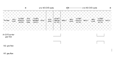
- FIG. 2 is a timing sequence of tungsten precursor, reducing agent, and nitrogen flows according to various embodiments.
- FIG. 3 is a process flow diagram showing relevant operations of methods according to various embodiments.
- FIG. 4A is a graph illustrating the effect of temperature on resistivity and roughness on N2-pulsed CVD deposition of tungsten.
- FIG. 4B is a graph illustrating the effect of pressure on resistivity and roughness on N2-pulsed CVD deposition of tungsten.
- FIGS. 5A and 5B are graphs illustrating the effect of nitrogen flow rate on resistivity and roughness on N2-pulsed CVD deposition of tungsten.
- FIG. 6 is a graph showing resistivity and roughness of tungsten films deposited by various processes.
- FIG. 7 is a block diagram of a processing system suitable for conducting tungsten deposition process in accordance with embodiments of the invention.
- Embodiments of the present invention involve depositing tungsten layers that have low resistivity and low roughness.
- low resistivity tungsten film has been achieved by growing large tungsten grains. This, however, increases the roughness of the film.
- percentage root mean square (RMS) roughness to film thickness may exceed 10% for a low resistivity tungsten film of 500 A or greater film. Lowering the roughness of the film makes subsequent operations (patterning, etc.) easier.
- RMS root mean square
- the methods described herein involve chemical vapor deposition of tungsten by reduction of tungsten by a reducing agent in the presence of alternating nitrogen gas pulses at high temperature and/or pressure.
- FIG. 1 shows a process according to certain embodiments of the invention.
- Deposition begins by a chemical vapor deposition (CVD) process in which a tungsten-containing precursor is reduced by hydrogen to deposit tungsten.
- CVD chemical vapor deposition
- WF6 tungsten hexafluoride
- the process may be performed with other tungsten precursors, including, but not limited to, WC16.
- hydrogen is generally used as the reducing agent in the CVD deposition of the bulk tungsten layer, other reducing agents including silane may be used in addition or instead of hydrogen without departing from the scope of the invention.
- W(CO)6 may be used with or without a reducing agent.
- N2 exposure may also be derived from exposure to other carrier gases that contain nitrogen, including NH3.
- NH3 or other types of nitrogen-containing precursors, the process described may be modified to deposit tungsten nitride with similar advantages.
- the WF 6 and H 2 are simultaneously introduced into the reaction chamber. This produces a continuous chemical reaction of mix reactant gases that continuously forms tungsten film on the substrate surface.
- the CVD deposition begins in an operation 101 in which the tungsten-containing precursor and hydrogen are introduced into the reaction chamber without any nitrogen being present.
- argon or another carrier gas is used as a carrier gas.
- the gases may be pre-mixed or not.
- the gases are allowed to react to deposit a portion of the desired total thickness of tungsten.
- the amount of tungsten deposited in this operation depends in part on the total desired thickness. For example, in certain embodiments, about 100 ⁇ is deposited in this operation.
- the tungsten film deposited in operation 101 may be deposited over a tungsten nucleation layer deposited in a previous process. This is described further below.
- the subsequent CVD depositions in FIG. 1 do not include further nucleation layer depositions; rather tungsten formed by each CVD operation is formed directly on the tungsten formed by the previous operation in FIG. 1 .
- an operation 103 another portion of the tungsten layer is deposited by H2 reduction of WF6 or other tungsten-precursor, in the presence of nitrogen.
- transitioning from operation 101 (H2-WF6 reduction/no N2) to operation 103 (H2-WF6 reduction/N2) involves turning on a flow of N2 into the chamber, such that N2, H2 and WF6 are all flowing into the chamber.
- the argon or other gas flow may be reduced or stopped during this portion of the process to compensate for the additional N2 gas introduced, thereby balancing the flows.
- One or more of the WF6 and the H2 may be stopped after operation 101 and started again for operation 103 .
- Another portion of the tungsten layer is deposited in this operation.
- High pressure is between 40 torr and 500 torr. In some embodiments, the pressure is between about 60 torr and 150 torr, or between about 80 torr and 100 torr.
- High temperature may be between about 350° C. and 500° C. In some embodiments, the temperature is at least about 420° C., or greater than 430°, e.g., between 440° C. and 460° C. In some embodiments, only one of high temperature and high pressure may be employed in certain embodiments. In certain embodiments, temperature and pressure generally remain constant throughout the process in FIG. 1 . As discussed further below, in certain embodiments, the use of high pressure, high temperature and alternating nitrogen exposure together provides low resistivity and low roughness levels otherwise unattainable.
- the process ends here.
- thick films e.g., 1000 ⁇
- more cycles are performed. This is indicated at an operation 105 , in which H2-WF6 reduction CVD without nitrogen present is again performed at high pressure and temperature. Transitioning from operation 103 to operation 105 typically involves turning off the flow of nitrogen, and if necessary, re-introducing any flow of argon or other gas that was reduced or stopped during or after operation 103 .
- Another portion of the tungsten layer is deposited. This is followed by another portion of the tungsten layer being deposited by H2 reduction of WF6 or other tungsten-precursor, in the presence of nitrogen in an operation 107 at high pressure and/or temperature.
- One or more additional cycles of N2 and no-N2 H2 reductions of WF6 are then performed if necessary to reach the desired thickness in operation 109 .
- the process may also end after repeating only operation 105 on the final cycle.
- the CVD deposition may begin with a N2 H2 reduction.
- pulses of N2 and tungsten containing precursor are simultaneously introduced into the chamber (e.g., with N2 as the carrier gas for the tungsten precursor) with delays such that pulsed N2-present reduction operations are performed without any intervening H2-only reduction operations.
- FIG. 2 shows an example of a timing sequence according to certain embodiments of the invention.
- a pre-heat and first H2 (no N2) reduction may occur as indicated. Both the pre-heat and the first deposition are optional.
- pre-heating the wafer to the process temperature assists in decreasing resistance non-uniformity.
- the tungsten precursor agent may be diverted to a process vacuum pump. This allows the flow to stabilize before introducing the precursor into the deposition chamber. In the embodiment depicted in FIG.
- the WF6 flow is diverted before and after each CVD deposition, with the WF6 flowed into the chamber during the deposition.
- Two cycles of the N2-CVD deposition are depicted in FIG. 2 , though the number of N2-CVD cycles may range from 1 to any desired number. It has been found that multiple N2-CVD cycles, e.g., 2-5, improve the roughness over a single cycle.
- Each N2-CVD cycle has a H2-only reduction, followed by a delay (delay 1). This delay may range from 0-1 min, e.g., 2 or 3 seconds. Note that although depicted sequentially, the WF6 divert and the delays are typically concurrent, i.e., the WF6 is diverted during the delay between reductions.
- each N2-CVD cycle also has a H2 reduction with N2, also followed by a delay (delay 2).
- delay 2 A delay of at least 1-3 seconds has been shown to improve the roughness over processes that do not have a delay after the N2-present H2 reduction. It is believed that this is due to the nitrogen remaining in the chamber passivating the surface of the deposited film, allowing the following H2-only film to deposit in a smoother fashion.
- Tungsten precursor flow is indicated on the timing sequence.
- Argon or other carrier gas, hydrogen and nitrogen flow into the chamber is indicated below the sequence.
- argon flow remains constant, except for the H2 reduction in N2, in which it is reduced or stopped to account for the additional N2 gas.
- H2 remains constant throughout the process, while N2 is flowed only during the H2 reduction in the presence of N2.
- the tungsten hexafluoride may also be flowed throughout each cycle and/or the hydrogen reducing agent may be diverted during the delay between WF6 reductions.
- FIG. 3 provides a process flow diagram according to various embodiments.
- the process begins by depositing a tungsten nucleation layer on a substrate in an operation 301 .
- a nucleation layer is a thin conformal layer which serves to facilitate the subsequent formation of a bulk material thereon.
- the nucleation layer is deposited using a pulsed nucleation layer (PNL) technique.
- PNL pulsed nucleation layer
- pulses of the reducing agent, purge gases, and tungsten-containing precursors are sequentially injected into and purged from the reaction chamber. The process is repeated in a cyclical fashion until the desired thickness is achieved.
- PNL broadly embodies any cyclical process of sequentially adding reactants for reaction on a semiconductor substrate.
- the tungsten (W) contact or line resistance increases due to scattering effects in the thinner W film.
- efficient tungsten deposition processes require tungsten nucleation layers, these layers typically have higher electrical resistivities than the bulk tungsten layers. Low resistivity tungsten films minimize power losses and overheating in integrated circuit designs. Because the ⁇ nucleation > ⁇ bulk , the thickness of the nucleation layer should be minimized to keep the total resistance as low as possible. On the other hand, the tungsten nucleation should be sufficiently thick to fully cover the underlying substrate to support high quality bulk deposition.
- the substrate temperature is low—below about 350° C., for example between about 250° C. and 350° C. or 250° C. and 325° C. In certain embodiments, the temperature is around 300° C.
- boron-containing (e.g., diborane) reducing agents can be used to deposit the nucleation layers, with the substrate exposed to alternating boron-containing reducing agent and tungsten-containing precursor pulses.
- Other reducing agents may be used instead of or in addition to boron-containing reducing agents.
- the substrate can be exposed to alternating silane and tungsten-containing precursor pulses in addition to or instead of alternating boron-containing reducing agent and tungsten-containing precursor pulses.
- the nucleation layer may be between about 3 ⁇ and 50 ⁇ , depending on the particular application and substrate.
- the nucleation layer may be as thin as 3 ⁇ -5 ⁇ , while a thicker nucleation layer, e.g., about 10 ⁇ , may be used for feature fill applications.
- methods for depositing tungsten nucleation layers in very small/high aspect ratio features as described in U.S. Pat. No. 7,955,972 are used to deposit the nucleation layer. These methods involve using PNL cycles of a boron-containing reducing agent and a tungsten-containing precursor with no hydrogen in the background to deposit very thin tungsten nucleation layers in these features that have good step coverage.
- the pressure or temperature during the process in FIG. 3 is held constant.
- high pressure as described above with respect to FIG. 1 is used for all operations in FIG. 3 , including operation 301 .
- the pressure during operation 301 may be between about 60 torr and 150 torr.
- temperature is held constant throughout the process described in FIG. 3 .
- Relatively low temperatures for operation 301 are described above. These may be used throughout the process in certain embodiments, including during operations 303 - 307 .
- Relatively high temperatures are described with reference to FIG. 1 . These may be used throughout the process in certain embodiments.
- pressure may be varied.
- the methods described herein are not limited to a particular method of tungsten nucleation layer deposition, but include deposition of bulk tungsten film on tungsten nucleation layers formed by any method including PNL, atomic layer deposition (ALD), CVD, and any other method.
- an optional operation 303 involves a treatment process to lower resistivity.
- treatment process such are described in such as that described in U.S. Pat. Nos. 7,772,114, and 8,058,170, incorporated by reference herein.
- the treatment process described therein involves exposing the deposited nucleation layer to multiple pulses of a reducing agent (with or without intervening pulses of another reactive compound).
- the substrate having the nucleation layer deposited thereon is exposed to multiple cycles of reducing agent pulses, or in some embodiments, alternating reducing agent and a tungsten-containing precursor pulses.
- the pulse times are shorter than those employed in operation 301 . For example, a 1 s pulse time may be employed in operation 303 and 2 s pulse in operation 301 .
- multiple pulses of diborane or other boron-containing reducing agents without intervening pulses of a tungsten-containing precursor are employed.
- the treatment process can be performed at a temperatures ranging from 375° C. to 415° C., e.g., about 395° C. If the nucleation layer is formed at a lower temperature, transitioning from nucleation layer deposition to this treatment operation may involve heating the substrate to between about 350° C. and 415° C., or in certain embodiments to about 375° C. to 415° C. and allowing it to stabilize before exposing the nucleation layer to a plurality of reducing agent or reducing agent/tungsten-containing precursor pulses.
- the substrate temperature is about 395° C. Lower temperatures may be used with longer pulse times to achieve equivalent treatment effect.
- the pressure may be relatively high, e.g., above 40 torr, above about 60 torr, or above about 80 torr. In embodiments in which temperature is held constant throughout the process in FIG. 3 , the temperature may range from about 250° C. to 500° C.
- the operation 303 lowers resistivity of the tungsten film deposited in FIG. 3 .
- operation 303 may delay nucleation and/or allow nuclei to coalesce thereby contributing to the growth of large grains and lowering resistivity.
- Higher pressure as described above with respect to FIG. 1 is beneficial for this operation.
- the treatment process described in operation 303 may be used to lower resistivity, in some embodiments the methods described herein can be implemented without it.
- An optional CVD process may be performed in an operation 305 . If performed, operation 305 is performed at low temperature and/or with no N2 present during the deposition. As with the CVD deposition described in FIG. 1 , operation 305 can involve WF6 reduction by H2. This operation can bolster the nucleation layer, improve uniformity and/or lower resistivity. For deposition of planar or blanket films, operation 305 can be used to deposit a film of about 10 ⁇ to 100 ⁇ in some embodiments, for example, 20 ⁇ . For feature fill, operation 305 can deposit a film thick enough to entirely or substantially fill the feature(s). Reduced temperature CVD operations for feature fill are described in U.S. patent application Ser. No. 12/755,248, incorporated by reference herein, and can include CVD depositions between 250° C. and 340° C., e.g., at 300° C. The pressure during operation 305 , if performed, can be high as described above.
- a bulk tungsten layer can be deposited by H2 reduction with alternating pulses of N2 at high temperature and/or high pressure in an operation 307 . This is described above with respect to FIG. 1 . Thickness can be deposited as appropriate for the application.
- FIGS. 1-3 can be performed to deposit blanket films and for feature fill.
- pressure and temperature lower than the high temperature and pressure regimes described above with respect to FIG. 1 are employed. It would be expected that the high pressures and temperatures would result in poor step coverage for feature fill, as the sticking coefficient increases at high pressure and reaction rate increases at high temperature, with high sticking coefficient and reaction rate resulting in more deposition at the top of a feature, reducing step coverage.
- high pressure and/or high temperature with the N2 pulsing has been found to result in low resistivity and/or low roughness films for blanket and feature fill applications, and to provide good step coverage.
- Resistivity was also measured for the deposited films with results shown in FIGS. 4A and 4B .
- the effect of temperature is shown in FIG. 4A , with the effect of pressure shown in FIG. 4B .
- FIG. 4A shows that increasing temperature lowers resistivity, with FIG. 4B showing that increasing pressure also lowers resistivity.
- the roughness results are also shown in FIGS. 4A and 4B to illustrate that resistivity and roughness both decrease. This is notable in that it would be expected that roughness and resistivity would be negatively correlated, with large grain size lowering resistivity and increasing roughness and small grain sizes increasing resistivity and lowering roughness.
- 300 ⁇ and 450 ⁇ thick blanket films were deposited using N2 pulsing as described above with respect to FIG. 2 at different N2 flow rates with resistivity and RMS roughness measured. Temperature and pressure were 445° C. and 90 Torr, respectively. The results for the 300 ⁇ are shown in FIG. 5A and for the 450 ⁇ in FIG. 5B . The results show that the addition of N2 helps reduce the tungsten roughness.
- FIG. 6 shows roughness and resistivity results for the following processes:
- B indicates a diborane pulse
- W indicates a tungsten hexafluoride pulse
- S indicates a silane pulse.
- x indicates multiple cycles. While resistivity can be improved at the expense of roughness, or vice versa, using the processes A-D, process E, in which the bulk CVD layer is deposited by H2 reduction of WF6 with and without N2 at high pressure and temperature results in both the lowest resistivity and roughness of all processes.
- the opening of the plugfill feature was 80 nm with a depth of 430 nm. Tungsten film step coverage was 100%.
- the methods of the invention may be carried out in various types of deposition apparatus available from various vendors.
- suitable apparatus include a Novellus Concept-1 Altus, a Concept 2 Altus, a Concept-2 ALTUS-S, a Concept 3 Altus deposition system, or any of a variety of other commercially available CVD tools.
- the process can be performed on multiple deposition stations sequentially. See, e.g., U.S. Pat. No. 6,143,082, which is incorporated herein by reference for all purposes.
- the pulsed nucleation process is performed at a first station that is one of two, five or even more deposition stations positioned within a single deposition chamber.
- the reducing gases and the tungsten-containing gases are alternately introduced to the surface of the semiconductor substrate, at the first station, using an individual gas supply system that creates a localized atmosphere at the substrate surface.
- Another station may be used to for a treatment operation as described above.
- One or more stations can then be used to perform CVD as described above.
- Two or more stations may be used to perform CVD in a parallel processing.
- a wafer may be indexed to have the CVD operations performed over two or more stations sequentially.
- FIG. 7 is a block diagram of a processing system suitable for conducting tungsten thin film deposition processes in accordance with embodiments of the invention.
- the system 700 includes a transfer module 703 .
- the transfer module 703 provides a clean, pressurized environment to minimize the risk of contamination of substrates being processed as they are moved between the various reactor modules.
- Mounted on the transfer module 703 is a multi-station reactor 709 capable of performing PNL deposition, multi-pulse treatment if desired, and CVD according to embodiments of the invention.
- Chamber 709 may include multiple stations 711 , 713 , 715 , and 717 that may sequentially perform these operations.
- chamber 709 could be configured such that station 711 performs PNL deposition, station 713 performs multi-pulse treatment, and stations 715 and 717 can perform N2-pulsed CVD.
- station 715 can perform N2-free CVD, and 717 can perform N2-pulsed CVD.
- the transfer module 703 may be one or more single or multi-station modules 707 capable of performing plasma or chemical (non-plasma) pre-cleans.
- the module may also be used for various other treatments, e.g., post liner tungsten nitride treatments.
- the system 700 also includes one or more (in this case two) wafer source modules 701 where wafers are stored before and after processing.
- An atmospheric robot (not shown) in the atmospheric transfer chamber 719 first removes wafers from the source modules 701 to loadlocks 721 .
- a wafer transfer device (generally a robot arm unit) in the transfer module 703 moves the wafers from loadlocks 721 to and among the modules mounted on the transfer module 703 .
- a system controller 750 is employed to control process conditions during deposition.
- the controller will typically include one or more memory devices and one or more processors.
- the processor may include a CPU or computer, analog and/or digital input/output connections, stepper motor controller boards, etc.
- the controller may control all of the activities of the deposition apparatus.
- the system controller executes system control software including sets of instructions for controlling the timing, mixture of gases, chamber pressure, chamber temperature, wafer temperature, RF power levels, wafer chuck or pedestal position, and other parameters of a particular process.
- Other computer programs stored on memory devices associated with the controller may be employed in some embodiments.
- the user interface may include a display screen, graphical software displays of the apparatus and/or process conditions, and user input devices such as pointing devices, keyboards, touch screens, microphones, etc.
- the computer program code for controlling the deposition and other processes in a process sequence can be written in any conventional computer readable programming language: for example, assembly language, C, C++, Pascal, Fortran or others. Compiled object code or script is executed by the processor to perform the tasks identified in the program.
- the controller parameters relate to process conditions such as, for example, process gas composition and flow rates, temperature, pressure, plasma conditions such as RF power levels and the low frequency RF frequency, cooling gas pressure, and chamber wall temperature. These parameters are provided to the user in the form of a recipe, and may be entered utilizing the user interface.
- Signals for monitoring the process may be provided by analog and/or digital input connections of the system controller.
- the signals for controlling the process are output on the analog and digital output connections of the deposition apparatus.
- the system software may be designed or configured in many different ways. For example, various chamber component subroutines or control objects may be written to control operation of the chamber components necessary to carry out the inventive deposition processes. Examples of programs or sections of programs for this purpose include substrate positioning code, process gas control code, pressure control code, heater control code, and plasma control code.
- a substrate positioning program may include program code for controlling chamber components that are used to load the substrate onto a pedestal or chuck and to control the spacing between the substrate and other parts of the chamber such as a gas inlet and/or target.
- a process gas control program may include code for controlling gas composition and flow rates and optionally for flowing gas into the chamber prior to deposition in order to stabilize the pressure in the chamber.
- a pressure control program may include code for controlling the pressure in the chamber by regulating, e.g., a throttle valve in the exhaust system of the chamber.
- a heater control program may include code for controlling the current to a heating unit that is used to heat the substrate. Alternatively, the heater control program may control delivery of a heat transfer gas such as helium to the wafer chuck.
- the apparatus/process described hereinabove may be used in conjunction with lithographic patterning tools or processes, for example, for the fabrication or manufacture of semiconductor devices, displays, LEDs, photovoltaic panels and the like. Typically, though not necessarily, such tools/processes will be used or conducted together in a common fabrication facility.
- Lithographic patterning of a film typically comprises some or all of the following steps, each step enabled with a number of possible tools: (1) application of photoresist on a workpiece, i.e., substrate, using a spin-on or spray-on tool; (2) curing of photoresist using a hot plate or furnace or UV curing tool; (3) exposing the photoresist to visible or UV or x-ray light with a tool such as a wafer stepper; (4) developing the resist so as to selectively remove resist and thereby pattern it using a tool such as a wet bench; (5) transferring the resist pattern into an underlying film or workpiece by using a dry or plasma-assisted etching tool; and (6) removing the resist using a tool such as an RF or microwave plasma resist stripper.
- a tool such as an RF or microwave plasma resist stripper.
- the present invention may be used to deposit thin, low resistivity tungsten layers for many different applications.
- One application is for interconnects in integrated circuits such as memory chips and microprocessors.
- Interconnects are current lines found on a single metallization layer and are generally long thin flat structures. These may be formed by a blanket deposition of a tungsten layer (by a process as described above), followed by a patterning operation that defines the location of current carrying tungsten lines and removal of the tungsten from regions outside the tungsten lines.
- a primary example of an interconnect application is a bit line in a memory chip.
- the invention is not limited to interconnect applications and extends to vias, contacts and other tungsten structures commonly found in electronic devices. In general, the invention finds application in any environment where thin, low-resistivity tungsten layers are required. Another example is for plugfill or other feature fill applications.
- the roughness of the tungsten layer is not greater than about 10% of the total thickness of the deposited tungsten layer, and more preferably not greater than about 5% of the total thickness of the deposited tungsten layer.
- the roughness of a tungsten layer can be measured by various techniques such as atomic force microscopy.
Abstract
Description
| TABLE 1 |
| Temperature Effect on Roughness |
| N2-pulse CVD Temperature (° C.) | Roughness at 450 Å (nm) | ||
| 300 | 6.6 | ||
| 395 | 4.3 | ||
| 430 | 3.1 | ||
| 445 | 1.9 | ||
| TABLE 1 |
| Pressure Effect on Roughness |
| N2-pulse CVD Pressure (torr) | Roughness at 450 Å (nm) | ||
| 40 | 3.6 | ||
| 60 | 3.1 | ||
| 90 | 1.9 | ||
| TABLE 3 |
| Process conditions |
| Nucleation | Treatment | Bulk CVD layer | ||
| A | B/W/S/W + | none | H2 reduction of WF6; no |
| x(S/W) in H2 | N2; ~400° C. and 40 torr | ||
| ambient; 300° C.; | |||
| 40 Torr | |||
| B | x(B/W) in H2- | x(B/W) at | H2 reduction of WF6; no |
| free ambient; | 395° C. | N2; ~400° C. and 40 torr | |
| 300° C.; 40 Torr | |||
| C | x(B/W) in H2- | x(B/W) at | H2 reduction of WF6; pulsed |
| free ambient; | 395° C. | N2; ~400° C. and 40 torr | |
| 300° C.; 40 Torr | |||
| D | B/W + x(S/W) | x(B/W) at | H2 reduction of WF6; pulsed |
| in H2 ambient; | 395° C. | N2; ~400° C. and 40 torr | |
| 300° C.; 40 Torr | |||
| E | x(B/W) in H2 | x(B/W) at | H2 reduction of WF6; pulsed N2; |
| ambient; 300° C.; | 395° C. | 445° C. and 90 torr | |
| 90 Torr | |||
| F | x(B/W) in H2 | x(B/W) at | H2 reduction of WF6; no N2; |
| ambient; 300° C.; | 395° C. | 445° C. and 95 torr | |
| 80 Torr | |||
| G | x(B/W) in H2 | x(B/W) at | H2 reduction of WF6; N2 during |
| ambient; 300° C.; | 395° C. | second half of deposition; 445° C. | |
| 80 Torr | and 95 torr | ||
| Thickness (Å) | Rt (micro-ohm-cm) | RMS (nm) | ||
| Blanket | 450 | 8.60 | 1.97 | ||
| Plugfill | 478 | 9.54 | 1.80 | ||
Claims (19)
Priority Applications (3)
| Application Number | Priority Date | Filing Date | Title |
|---|---|---|---|
| US13/633,798 US8853080B2 (en) | 2012-09-09 | 2012-10-02 | Method for depositing tungsten film with low roughness and low resistivity |
| KR1020130108151A KR20140034081A (en) | 2012-09-09 | 2013-09-09 | Method for depositing tungsten film with low roughness and low resistivity |
| TW102132433A TWI605522B (en) | 2012-09-09 | 2013-09-09 | Method for depositing tungsten film with low roughness and low resistivity |
Applications Claiming Priority (2)
| Application Number | Priority Date | Filing Date | Title |
|---|---|---|---|
| US201261698700P | 2012-09-09 | 2012-09-09 | |
| US13/633,798 US8853080B2 (en) | 2012-09-09 | 2012-10-02 | Method for depositing tungsten film with low roughness and low resistivity |
Publications (2)
| Publication Number | Publication Date |
|---|---|
| US20140073135A1 US20140073135A1 (en) | 2014-03-13 |
| US8853080B2 true US8853080B2 (en) | 2014-10-07 |
Family
ID=50233683
Family Applications (1)
| Application Number | Title | Priority Date | Filing Date |
|---|---|---|---|
| US13/633,798 Active US8853080B2 (en) | 2012-09-09 | 2012-10-02 | Method for depositing tungsten film with low roughness and low resistivity |
Country Status (3)
| Country | Link |
|---|---|
| US (1) | US8853080B2 (en) |
| KR (1) | KR20140034081A (en) |
| TW (1) | TWI605522B (en) |
Cited By (22)
| Publication number | Priority date | Publication date | Assignee | Title |
|---|---|---|---|---|
| US9153486B2 (en) | 2013-04-12 | 2015-10-06 | Lam Research Corporation | CVD based metal/semiconductor OHMIC contact for high volume manufacturing applications |
| US9159571B2 (en) | 2009-04-16 | 2015-10-13 | Lam Research Corporation | Tungsten deposition process using germanium-containing reducing agent |
| US9236297B2 (en) | 2009-04-16 | 2016-01-12 | Novellus Systems, Inc. | Low tempature tungsten film deposition for small critical dimension contacts and interconnects |
| US9240347B2 (en) | 2012-03-27 | 2016-01-19 | Novellus Systems, Inc. | Tungsten feature fill |
| US9349637B2 (en) | 2014-08-21 | 2016-05-24 | Lam Research Corporation | Method for void-free cobalt gap fill |
| US9583385B2 (en) | 2001-05-22 | 2017-02-28 | Novellus Systems, Inc. | Method for producing ultra-thin tungsten layers with improved step coverage |
| US9589808B2 (en) | 2013-12-19 | 2017-03-07 | Lam Research Corporation | Method for depositing extremely low resistivity tungsten |
| US9613818B2 (en) | 2015-05-27 | 2017-04-04 | Lam Research Corporation | Deposition of low fluorine tungsten by sequential CVD process |
| US9748137B2 (en) | 2014-08-21 | 2017-08-29 | Lam Research Corporation | Method for void-free cobalt gap fill |
| US9754824B2 (en) | 2015-05-27 | 2017-09-05 | Lam Research Corporation | Tungsten films having low fluorine content |
| US20170309490A1 (en) * | 2014-09-24 | 2017-10-26 | Hitachi Kokusai Electric Inc. | Method of manufacturing semiconductor device |
| US9953984B2 (en) | 2015-02-11 | 2018-04-24 | Lam Research Corporation | Tungsten for wordline applications |
| US9978605B2 (en) | 2015-05-27 | 2018-05-22 | Lam Research Corporation | Method of forming low resistivity fluorine free tungsten film without nucleation |
| US9997405B2 (en) | 2014-09-30 | 2018-06-12 | Lam Research Corporation | Feature fill with nucleation inhibition |
| US10170320B2 (en) | 2015-05-18 | 2019-01-01 | Lam Research Corporation | Feature fill with multi-stage nucleation inhibition |
| US10211099B2 (en) | 2016-12-19 | 2019-02-19 | Lam Research Corporation | Chamber conditioning for remote plasma process |
| US10256142B2 (en) | 2009-08-04 | 2019-04-09 | Novellus Systems, Inc. | Tungsten feature fill with nucleation inhibition |
| US10381266B2 (en) | 2012-03-27 | 2019-08-13 | Novellus Systems, Inc. | Tungsten feature fill with nucleation inhibition |
| US10573522B2 (en) | 2016-08-16 | 2020-02-25 | Lam Research Corporation | Method for preventing line bending during metal fill process |
| US11348795B2 (en) | 2017-08-14 | 2022-05-31 | Lam Research Corporation | Metal fill process for three-dimensional vertical NAND wordline |
| US11437269B2 (en) | 2012-03-27 | 2022-09-06 | Novellus Systems, Inc. | Tungsten feature fill with nucleation inhibition |
| US11549175B2 (en) | 2018-05-03 | 2023-01-10 | Lam Research Corporation | Method of depositing tungsten and other metals in 3D NAND structures |
Families Citing this family (9)
| Publication number | Priority date | Publication date | Assignee | Title |
|---|---|---|---|---|
| KR102076087B1 (en) * | 2013-08-19 | 2020-02-11 | 어플라이드 머티어리얼스, 인코포레이티드 | Apparatus for impurity layered epitaxy |
| WO2015080058A1 (en) * | 2013-11-27 | 2015-06-04 | 東京エレクトロン株式会社 | Method for forming tungsten film |
| US9595470B2 (en) * | 2014-05-09 | 2017-03-14 | Lam Research Corporation | Methods of preparing tungsten and tungsten nitride thin films using tungsten chloride precursor |
| CN106653678A (en) * | 2015-11-03 | 2017-05-10 | 中芯国际集成电路制造(上海)有限公司 | Conductive plug structure and forming method thereof |
| KR102466639B1 (en) | 2017-04-10 | 2022-11-11 | 램 리써치 코포레이션 | Low resistivity films containing molybdenum |
| JP7018748B2 (en) * | 2017-11-28 | 2022-02-14 | 東京エレクトロン株式会社 | Film formation method and calculation method of film formation conditions |
| KR20210007031A (en) * | 2018-06-07 | 2021-01-19 | 램 리써치 코포레이션 | Reduction of diffusion across membrane interfaces |
| US11205589B2 (en) * | 2019-10-06 | 2021-12-21 | Applied Materials, Inc. | Methods and apparatuses for forming interconnection structures |
| US20220068709A1 (en) * | 2020-08-25 | 2022-03-03 | Applied Materials, Inc. | Low Resistivity Tungsten Film And Method Of Manufacture |
Citations (165)
| Publication number | Priority date | Publication date | Assignee | Title |
|---|---|---|---|---|
| US4746375A (en) | 1987-05-08 | 1988-05-24 | General Electric Company | Activation of refractory metal surfaces for electroless plating |
| US4804560A (en) | 1986-03-17 | 1989-02-14 | Fujitsu Limited | Method of selectively depositing tungsten upon a semiconductor substrate |
| US4874719A (en) | 1986-05-06 | 1989-10-17 | Kabushiki Kaisha Toshiba | Method for manufacturing an electrical connection between conductor levels |
| US5028565A (en) | 1989-08-25 | 1991-07-02 | Applied Materials, Inc. | Process for CVD deposition of tungsten layer on semiconductor wafer |
| US5227329A (en) | 1990-08-31 | 1993-07-13 | Hitachi, Ltd. | Method of manufacturing semiconductor device |
| US5250467A (en) | 1991-03-29 | 1993-10-05 | Applied Materials, Inc. | Method for forming low resistance and low defect density tungsten contacts to silicon semiconductor wafer |
| US5250329A (en) | 1989-04-06 | 1993-10-05 | Microelectronics And Computer Technology Corporation | Method of depositing conductive lines on a dielectric |
| US5308655A (en) | 1991-08-16 | 1994-05-03 | Materials Research Corporation | Processing for forming low resistivity titanium nitride films |
| US5326723A (en) | 1992-09-09 | 1994-07-05 | Intel Corporation | Method for improving stability of tungsten chemical vapor deposition |
| US5370739A (en) | 1992-06-15 | 1994-12-06 | Materials Research Corporation | Rotating susceptor semiconductor wafer processing cluster tool module useful for tungsten CVD |
| US5391394A (en) | 1990-01-08 | 1995-02-21 | Lsi Logic Corporation | Tungsten deposition process for low contact resistivity to silicon |
| JPH08115984A (en) | 1994-10-17 | 1996-05-07 | Hitachi Ltd | Semiconductor device and its manufacture |
| US5567583A (en) | 1991-12-16 | 1996-10-22 | Biotronics Corporation | Methods for reducing non-specific priming in DNA detection |
| JPH0927596A (en) | 1995-07-11 | 1997-01-28 | Sanyo Electric Co Ltd | Manufacture of semiconductor device |
| US5661080A (en) | 1992-12-10 | 1997-08-26 | Hyundai Electronics Industries Co., Ltd. | Method for fabricating tungsten plug |
| US5726096A (en) | 1993-12-17 | 1998-03-10 | Hyundai Electronics Industries Co., Ltd. | Method for forming a tungsten silicide layer in a semiconductor device |
| JPH10144688A (en) | 1996-11-02 | 1998-05-29 | Hyundai Electron Ind Co Ltd | Method of forming contact plugs of semiconductor device having contact holes different in size |
| US5795824A (en) | 1997-08-28 | 1998-08-18 | Novellus Systems, Inc. | Method for nucleation of CVD tungsten films |
| US5804249A (en) | 1997-02-07 | 1998-09-08 | Lsi Logic Corporation | Multistep tungsten CVD process with amorphization step |
| US5817576A (en) | 1994-09-27 | 1998-10-06 | Applied Materials, Inc. | Utilization of SiH4 soak and purge in deposition processes |
| US5833817A (en) | 1996-04-22 | 1998-11-10 | Taiwan Semiconductor Manufacturing Company, Ltd. | Method for improving conformity and contact bottom coverage of sputtered titanium nitride barrier layers |
| WO1998051838A1 (en) | 1997-05-16 | 1998-11-19 | Applied Materials, Inc. | Low resistivity w using b2h¿6? |
| US5913145A (en) | 1997-08-28 | 1999-06-15 | Texas Instruments Incorporated | Method for fabricating thermally stable contacts with a diffusion barrier formed at high temperatures |
| US5926720A (en) | 1997-09-08 | 1999-07-20 | Lsi Logic Corporation | Consistent alignment mark profiles on semiconductor wafers using PVD shadowing |
| US5956609A (en) | 1997-08-11 | 1999-09-21 | Taiwan Semiconductor Manufacturing Company, Ltd. | Method for reducing stress and improving step-coverage of tungsten interconnects and plugs |
| JPH11330006A (en) | 1998-04-30 | 1999-11-30 | Internatl Business Mach Corp <Ibm> | Ultrathin single phase barrier layer for conductor and its manufacturing method |
| US6001729A (en) | 1995-01-10 | 1999-12-14 | Kawasaki Steel Corporation | Method of forming wiring structure for semiconductor device |
| US6017818A (en) | 1996-01-22 | 2000-01-25 | Texas Instruments Incorporated | Process for fabricating conformal Ti-Si-N and Ti-B-N based barrier films with low defect density |
| US6034419A (en) | 1989-04-07 | 2000-03-07 | Inmos Limited | Semiconductor device with a tungsten contact |
| US6037263A (en) | 1998-11-05 | 2000-03-14 | Vanguard International Semiconductor Corporation | Plasma enhanced CVD deposition of tungsten and tungsten compounds |
| US6066366A (en) | 1998-07-22 | 2000-05-23 | Applied Materials, Inc. | Method for depositing uniform tungsten layers by CVD |
| JP2000208516A (en) | 1999-01-11 | 2000-07-28 | Nec Corp | Semiconductor device having multilayer wiring structure and manufacture thereof |
| US6099904A (en) | 1997-12-02 | 2000-08-08 | Applied Materials, Inc. | Low resistivity W using B2 H6 nucleation step |
| US6107200A (en) | 1998-03-12 | 2000-08-22 | Fujitsu Limited | Semiconductor device manufacturing method |
| JP2000235962A (en) | 1999-02-17 | 2000-08-29 | Ulvac Japan Ltd | Manufacture of barrier film |
| US6143082A (en) | 1998-10-08 | 2000-11-07 | Novellus Systems, Inc. | Isolation of incompatible processes in a multi-station processing chamber |
| US6174812B1 (en) | 1999-06-08 | 2001-01-16 | United Microelectronics Corp. | Copper damascene technology for ultra large scale integration circuits |
| WO2001027347A1 (en) | 1999-10-15 | 2001-04-19 | Asm Microchemistry Oy | Method of depositing transition metal nitride thin films |
| WO2001029893A1 (en) | 1999-10-15 | 2001-04-26 | Asm America, Inc. | Method for depositing nanolaminate thin films on sensitive surfaces |
| US6245654B1 (en) | 1999-03-31 | 2001-06-12 | Taiwan Semiconductor Manufacturing Company, Ltd | Method for preventing tungsten contact/via plug loss after a backside pressure fault |
| US20010008808A1 (en) | 1995-10-25 | 2001-07-19 | Fernando Gonzalez | A Method Of Fabricating A DRAM Transistor With A Dual Gate Oxide Technique |
| US6265312B1 (en) | 1999-08-02 | 2001-07-24 | Stmicroelectronics, Inc. | Method for depositing an integrated circuit tungsten film stack that includes a post-nucleation pump down step |
| US20010014533A1 (en) | 1999-01-08 | 2001-08-16 | Shih-Wei Sun | Method of fabricating salicide |
| US6277744B1 (en) | 2000-01-21 | 2001-08-21 | Advanced Micro Devices, Inc. | Two-level silane nucleation for blanket tungsten deposition |
| US20010015494A1 (en) | 1997-06-13 | 2001-08-23 | Kie Y. Ahn | Integrated circuit wiring with low rc time delay |
| US6294468B1 (en) | 1999-05-24 | 2001-09-25 | Agere Systems Guardian Corp. | Method of chemical vapor depositing tungsten films |
| US6297152B1 (en) | 1996-12-12 | 2001-10-02 | Applied Materials, Inc. | CVD process for DCS-based tungsten silicide |
| US6310300B1 (en) | 1996-11-08 | 2001-10-30 | International Business Machines Corporation | Fluorine-free barrier layer between conductor and insulator for degradation prevention |
| US6309966B1 (en) | 1999-09-03 | 2001-10-30 | Motorola, Inc. | Apparatus and method of a low pressure, two-step nucleation tungsten deposition |
| US20010044041A1 (en) | 2000-05-18 | 2001-11-22 | Badding Michael E. | High performance solid electrolyte fuel cells |
| EP1179838A2 (en) | 2000-07-31 | 2002-02-13 | Applied Materials, Inc. | Deposition of tungsten films from W(CO)6 |
| US6355558B1 (en) | 1999-06-10 | 2002-03-12 | Texas Instruments Incorporated | Metallization structure, and associated method, to improve crystallographic texture and cavity fill for CVD aluminum/PVD aluminum alloy films |
| US20020037630A1 (en) | 2000-06-08 | 2002-03-28 | Micron Technology, Inc. | Methods for forming and integrated circuit structures containing ruthenium and tungsten containing layers |
| WO2002041379A1 (en) | 2000-11-17 | 2002-05-23 | Tokyo Electron Limited | Method of forming metal wiring and semiconductor manufacturing apparatus for forming metal wiring |
| US6404054B1 (en) | 1998-10-28 | 2002-06-11 | Samsung Electronics Co., Ltd. | Tungsten layer formation method for semiconductor device and semiconductor device using the same |
| US20020090796A1 (en) | 1999-09-13 | 2002-07-11 | Applied Materials, Inc. | Silicon layer to improve plug filling by CVD |
| US6429126B1 (en) | 2000-03-29 | 2002-08-06 | Applied Materials, Inc. | Reduced fluorine contamination for tungsten CVD |
| US20020117399A1 (en) | 2001-02-23 | 2002-08-29 | Applied Materials, Inc. | Atomically thin highly resistive barrier layer in a copper via |
| US20020132472A1 (en) | 2001-03-14 | 2002-09-19 | Jusung Engineering Co., Ltd. | Method for forming metal plug |
| US6465347B2 (en) | 1998-12-18 | 2002-10-15 | Tokyo Electron Limited | Tungsten film forming method |
| US20020155722A1 (en) | 1999-08-24 | 2002-10-24 | Alessandra Satta | Method for bottomless deposition of barrier layers in integrated circuit metallization schemes |
| US20020168840A1 (en) | 2001-05-11 | 2002-11-14 | Applied Materials, Inc. | Deposition of tungsten silicide films |
| US20020177316A1 (en) | 2000-11-16 | 2002-11-28 | Miller Anne E. | Slurry and method for chemical mechanical polishing of copper |
| US20030059980A1 (en) | 2001-09-25 | 2003-03-27 | Ling Chen | Copper interconnect barrier layer structure and formation method |
| US6551929B1 (en) | 2000-06-28 | 2003-04-22 | Applied Materials, Inc. | Bifurcated deposition process for depositing refractory metal layers employing atomic layer deposition and chemical vapor deposition techniques |
| US20030091870A1 (en) | 2001-11-15 | 2003-05-15 | Siddhartha Bhowmik | Method of forming a liner for tungsten plugs |
| US6566262B1 (en) | 2001-11-01 | 2003-05-20 | Lsi Logic Corporation | Method for creating self-aligned alloy capping layers for copper interconnect structures |
| US6566250B1 (en) | 2002-03-18 | 2003-05-20 | Taiwant Semiconductor Manufacturing Co., Ltd | Method for forming a self aligned capping layer |
| US20030104126A1 (en) | 2001-10-10 | 2003-06-05 | Hongbin Fang | Method for depositing refractory metal layers employing sequential deposition techniques |
| US6581258B2 (en) | 2000-05-19 | 2003-06-24 | Murata Manufacturing Co., Ltd. | Method of forming electrode film |
| US20030123216A1 (en) | 2001-12-27 | 2003-07-03 | Yoon Hyungsuk A. | Deposition of tungsten for the formation of conformal tungsten silicide |
| US20030127043A1 (en) | 2001-07-13 | 2003-07-10 | Applied Materials, Inc. | Pulsed nucleation deposition of tungsten layers |
| US20030129828A1 (en) | 1999-10-02 | 2003-07-10 | Uri Cohen | Methods for making multiple seed layers for metallic interconnects |
| US6593233B1 (en) | 1995-03-03 | 2003-07-15 | Nec Electronics Corporation | Semiconductor device and method for manufacturing the same |
| US6627066B1 (en) | 1999-08-30 | 2003-09-30 | Ebara Corporation | Method of measuring the concentration of a leveler in a plating liquid |
| US20030190802A1 (en) | 2001-06-19 | 2003-10-09 | United Microelectronics Corp. | Method for forming a plug metal layer |
| US6635965B1 (en) | 2001-05-22 | 2003-10-21 | Novellus Systems, Inc. | Method for producing ultra-thin tungsten layers with improved step coverage |
| US20040014315A1 (en) | 2001-07-16 | 2004-01-22 | Applied Materials, Inc. | Formation of composite tungsten films |
| US20040044127A1 (en) | 2002-08-22 | 2004-03-04 | Konica Corporation | Organic-inorganic hybrid film, its manufacturing method, optical film, and polarizing film |
| US6706625B1 (en) | 2002-12-06 | 2004-03-16 | Chartered Semiconductor Manufacturing Ltd. | Copper recess formation using chemical process for fabricating barrier cap for lines and vias |
| US6720261B1 (en) | 1999-06-02 | 2004-04-13 | Agere Systems Inc. | Method and system for eliminating extrusions in semiconductor vias |
| US6740585B2 (en) | 2001-07-25 | 2004-05-25 | Applied Materials, Inc. | Barrier formation using novel sputter deposition method with PVD, CVD, or ALD |
| US6740221B2 (en) | 2001-03-15 | 2004-05-25 | Applied Materials Inc. | Method of forming copper interconnects |
| US20040142557A1 (en) | 2003-01-21 | 2004-07-22 | Novellus Systems, Inc. | Deposition of tungsten nitride |
| US6777331B2 (en) | 2000-03-07 | 2004-08-17 | Simplus Systems Corporation | Multilayered copper structure for improving adhesion property |
| JP2004235456A (en) | 2003-01-30 | 2004-08-19 | Seiko Epson Corp | Film depositing system, film depositing process, and process for manufacturing semiconductor device |
| US20040202786A1 (en) | 2001-05-22 | 2004-10-14 | Novellus Systems, Inc. | Method of forming low-resistivity tungsten interconnects |
| US20040206267A1 (en) | 2002-12-23 | 2004-10-21 | Sankar Sambasivan | Aluminum phosphate coatings |
| US6827839B2 (en) | 2000-11-02 | 2004-12-07 | Shipley Company, L.L.C. | Plating bath analysis |
| US6844258B1 (en) | 2003-05-09 | 2005-01-18 | Novellus Systems, Inc. | Selective refractory metal and nitride capping |
| US20050031786A1 (en) | 2001-05-22 | 2005-02-10 | Novellus Systems, Inc. | Method for reducing tungsten film roughness and improving step coverage |
| US6861356B2 (en) | 1997-11-05 | 2005-03-01 | Tokyo Electron Limited | Method of forming a barrier film and method of forming wiring structure and electrodes of semiconductor device having a barrier film |
| US20050059236A1 (en) | 2003-09-11 | 2005-03-17 | Akio Nishida | Semiconductor device and a method of manufacturing the same |
| US6903016B2 (en) | 1999-10-02 | 2005-06-07 | Uri Cohen | Combined conformal/non-conformal seed layers for metallic interconnects |
| US6905543B1 (en) | 2002-06-19 | 2005-06-14 | Novellus Systems, Inc | Methods of forming tungsten nucleation layer |
| US6908848B2 (en) | 2000-12-20 | 2005-06-21 | Samsung Electronics, Co., Ltd. | Method for forming an electrical interconnection providing improved surface morphology of tungsten |
| US20050136594A1 (en) | 2003-12-23 | 2005-06-23 | Hynix Semiconductor Inc. | Method for forming bit-line of semiconductor device |
| US20050179141A1 (en) | 2002-05-30 | 2005-08-18 | Yun Ju-Young | Methods of forming metal interconnections of semiconductor devices by treating a barrier metal layer |
| US6936538B2 (en) | 2001-07-16 | 2005-08-30 | Applied Materials, Inc. | Method and apparatus for depositing tungsten after surface treatment to improve film characteristics |
| KR20050087428A (en) | 2004-02-26 | 2005-08-31 | 노벨러스 시스템즈, 인코포레이티드 | Deposition of tungsten nitride |
| US20050191803A1 (en) * | 1997-11-05 | 2005-09-01 | Tokyo Electron Limited | Method of forming a metal film for electrode |
| US6962873B1 (en) | 2002-12-10 | 2005-11-08 | Novellus Systems, Inc. | Nitridation of electrolessly deposited cobalt |
| US20060003581A1 (en) | 2004-06-30 | 2006-01-05 | Johnston Steven W | Atomic layer deposited tantalum containing adhesion layer |
| US20060075966A1 (en) | 2002-01-26 | 2006-04-13 | Applied Materials, Inc. | Apparatus and method for plasma assisted deposition |
| KR20060074593A (en) | 2004-12-27 | 2006-07-03 | 동부일렉트로닉스 주식회사 | Apparatus and method for monitoring density end point in semiconductor device |
| KR20060087844A (en) | 2005-01-31 | 2006-08-03 | 삼성전자주식회사 | Semiconductor device and method for manufacturing the same |
| US7144488B2 (en) | 2002-06-05 | 2006-12-05 | Shipley Company, L.L.C. | Electrode, electrochemical cell, and method for analysis of electroplating baths |
| US20060284317A1 (en) | 2005-06-17 | 2006-12-21 | Fujitsu Limited | Semiconductor device and a fabrication process thereof |
| JP2007009298A (en) | 2005-07-01 | 2007-01-18 | Tokyo Electron Ltd | Method for depositing tungsten film, film deposition system, storage medium, and semiconductor device |
| JP2007507892A (en) | 2003-09-30 | 2007-03-29 | 東京エレクトロン株式会社 | A method of forming a metal layer using an intermittent precursor gas flow process. |
| US20070099420A1 (en) | 2005-11-02 | 2007-05-03 | Dominguez Juan E | Direct tailoring of the composition and density of ALD films |
| US7220671B2 (en) | 2005-03-31 | 2007-05-22 | Intel Corporation | Organometallic precursors for the chemical phase deposition of metal films in interconnect applications |
| US20070190780A1 (en) | 2003-06-18 | 2007-08-16 | Applied Materials, Inc. | Atomic layer deposition of barrier materials |
| JP2007250907A (en) | 2006-03-16 | 2007-09-27 | Renesas Technology Corp | Semiconductor device and manufacturing method therefor |
| JP2007251164A (en) | 2006-03-15 | 2007-09-27 | Internatl Business Mach Corp <Ibm> | Interconnect structure, semiconductor structure and method of forming interconnect structure (formation of oxidation-resistant seed layer for interconnect usage) |
| WO2007121249A3 (en) | 2006-04-11 | 2007-12-27 | Applied Materials Inc | Process for forming cobalt-containing materials |
| US20080045010A1 (en) | 2003-08-26 | 2008-02-21 | Novellus Systems, Inc. | Reducing silicon attack and improving resistivity of tungsten nitride film |
| US20080081127A1 (en) | 2006-09-28 | 2008-04-03 | Thompson David M | Organometallic compounds, processes for the preparation thereof and methods of use thereof |
| US20080124926A1 (en) | 2001-05-22 | 2008-05-29 | Novellus Systems, Inc. | Methods for growing low-resistivity tungsten film |
| US7416979B2 (en) | 2001-07-25 | 2008-08-26 | Applied Materials, Inc. | Deposition methods for barrier and tungsten materials |
| US7419904B2 (en) | 2004-04-12 | 2008-09-02 | Ulvac Inc. | Method for forming barrier film and method for forming electrode film |
| US7429402B2 (en) | 2004-12-10 | 2008-09-30 | Applied Materials, Inc. | Ruthenium as an underlayer for tungsten film deposition |
| US20080254619A1 (en) | 2007-04-14 | 2008-10-16 | Tsang-Jung Lin | Method of fabricating a semiconductor device |
| US20080254623A1 (en) | 2001-05-22 | 2008-10-16 | Novellus Systems, Inc. | Methods for growing low-resistivity tungsten for high aspect ratio and small features |
| US20080280438A1 (en) | 2000-06-28 | 2008-11-13 | Ken Kaung Lai | Methods for depositing tungsten layers employing atomic layer deposition techniques |
| US7465665B2 (en) | 2000-06-28 | 2008-12-16 | Applied Materials, Inc. | Method for depositing tungsten-containing layers by vapor deposition techniques |
| JP2009024252A (en) | 2007-05-15 | 2009-02-05 | Applied Materials Inc | Atomic layer deposition process for tungsten material |
| US20090053893A1 (en) | 2005-01-19 | 2009-02-26 | Amit Khandelwal | Atomic layer deposition of tungsten materials |
| US20090057151A1 (en) | 2007-08-27 | 2009-03-05 | Eci Technology, Inc. | Detection of additive breakdown products in acid copper plating baths |
| US7501344B2 (en) | 2000-06-27 | 2009-03-10 | Applied Materials, Inc. | Formation of boride barrier layers using chemisorption techniques |
| US20090149022A1 (en) | 2007-12-05 | 2009-06-11 | Novellus Systems, Inc. | Method for improving uniformity and adhesion of low resistivity tungsten film |
| US20090160030A1 (en) | 2005-09-01 | 2009-06-25 | Micron Technology, Inc. | Methods for forming through wafer interconnects and structures resulting therefrom |
| US20090163025A1 (en) | 2007-12-21 | 2009-06-25 | Novellus Systems, Inc. | Methods for forming all tungsten contacts and lines |
| US7563718B2 (en) | 2006-06-29 | 2009-07-21 | Hynix Semiconductor Inc. | Method for forming tungsten layer of semiconductor device and method for forming tungsten wiring layer using the same |
| KR20090103815A (en) | 2008-03-28 | 2009-10-01 | 도쿄엘렉트론가부시키가이샤 | Electrostatic chuck and manufacturing method thereof |
| US20090315154A1 (en) | 2008-06-19 | 2009-12-24 | Micron Technology, Inc. | Semiconductor with through-substrate interconnect |
| US7655567B1 (en) * | 2007-07-24 | 2010-02-02 | Novellus Systems, Inc. | Methods for improving uniformity and resistivity of thin tungsten films |
| US20100055904A1 (en) | 2008-08-29 | 2010-03-04 | Novellus Systems Inc. | Method for reducing tungsten roughness and improving reflectivity |
| US7675119B2 (en) | 2006-12-25 | 2010-03-09 | Elpida Memory, Inc. | Semiconductor device and manufacturing method thereof |
| US20100130003A1 (en) | 2008-11-25 | 2010-05-27 | Chuan-Yi Lin | Method of Forming Through-Silicon Vias |
| US7732327B2 (en) | 2000-06-28 | 2010-06-08 | Applied Materials, Inc. | Vapor deposition of tungsten materials |
| US20100159694A1 (en) | 2008-06-12 | 2010-06-24 | Novellus Systems Inc. | Method for depositing thin tungsten film with low resistivity and robust micro-adhesion characteristics |
| US7745329B2 (en) | 2002-02-26 | 2010-06-29 | Applied Materials, Inc. | Tungsten nitride atomic layer deposition processes |
| US20100199887A1 (en) | 2009-02-04 | 2010-08-12 | Sumitomo Chemical Company, Limited | Hydrophilizing agent, method of producing a hydrophilizing agent and hydrophilic product |
| US20100267235A1 (en) | 2009-04-16 | 2010-10-21 | Feng Chen | Methods for depositing ultra thin low resistivity tungsten film for small critical dimension contacts and interconnects |
| US20110059608A1 (en) | 2009-09-09 | 2011-03-10 | Novellus Systems, Inc. | Method for improving adhesion of low resistivity tungsten/tungsten nitride layers |
| US20110156154A1 (en) | 2009-12-30 | 2011-06-30 | Jan Hoentschel | High-k metal gate electrode structures formed at different process stages of a semiconductor device |
| US7977243B2 (en) | 2001-11-14 | 2011-07-12 | Canon Anelva Corporation | Barrier metal film production apparatus, barrier metal film production method, metal film production method, and metal film production apparatus |
| US20110221044A1 (en) | 2010-03-12 | 2011-09-15 | Michal Danek | Tungsten barrier and seed for copper filled tsv |
| US20110233778A1 (en) | 2010-03-24 | 2011-09-29 | Applied Materials, Inc. | Formation of liner and barrier for tungsten as gate electrode and as contact plug to reduce resistance and enhance device performance |
| US8062977B1 (en) | 2008-01-31 | 2011-11-22 | Novellus Systems, Inc. | Ternary tungsten-containing resistive thin films |
| US8087966B2 (en) | 2004-04-21 | 2012-01-03 | Koninklijke Philips Electronics N.V. | Method for the thermal treatment of tungsten electrodes free from thorium oxide for high-pressure discharge lamps |
| US20120009785A1 (en) | 2010-07-09 | 2012-01-12 | Anand Chandrashekar | Depositing Tungsten Into High Aspect Ratio Features |
| US8110877B2 (en) | 2008-12-19 | 2012-02-07 | Intel Corporation | Metal-insulator-semiconductor tunneling contacts having an insulative layer disposed between source/drain contacts and source/drain regions |
| US8258057B2 (en) | 2006-03-30 | 2012-09-04 | Intel Corporation | Copper-filled trench contact for transistor performance improvement |
| US20120231626A1 (en) | 2011-03-10 | 2012-09-13 | Applied Materials, Inc. | Formation of liner and barrier for tungsten as gate electrode and as contact plug to reduce resistance and enhance device performance |
| US20130109172A1 (en) | 2011-10-28 | 2013-05-02 | Joshua Collins | High temperature tungsten metallization process |
| WO2013090295A1 (en) | 2011-12-12 | 2013-06-20 | Novellus Systems, Inc. | Monitoring leveler concentrations in electroplating solutions |
| US20130171822A1 (en) | 2009-08-04 | 2013-07-04 | Anand Chandrashekar | Tungsten feature fill with nucleation inhibition |
| US20130168864A1 (en) | 2001-05-22 | 2013-07-04 | Sang-Hyeob Lee | Method for producing ultra-thin tungsten layers with improved step coverage |
| WO2013148880A1 (en) | 2012-03-27 | 2013-10-03 | Novellus Systems, Inc. | Tungsten feature fill |
| WO2013148444A1 (en) | 2012-03-27 | 2013-10-03 | Novellus Systems, Inc. | Tungsten feature fill with nucleation inhibition |
| US20140011358A1 (en) | 2012-06-29 | 2014-01-09 | Novellus Systems, Inc. | Methods of forming tensile tungsten films and compressive tungsten films |
| US20140027664A1 (en) | 2012-07-26 | 2014-01-30 | Lam Research Corporation | Ternary tungsten boride nitride films and methods for forming same |
| US20140030889A1 (en) | 2012-07-27 | 2014-01-30 | Feng Chen | Methods of improving tungsten contact resistance in small critical dimension features |
-
2012
- 2012-10-02 US US13/633,798 patent/US8853080B2/en active Active
-
2013
- 2013-09-09 KR KR1020130108151A patent/KR20140034081A/en not_active IP Right Cessation
- 2013-09-09 TW TW102132433A patent/TWI605522B/en active
Patent Citations (225)
| Publication number | Priority date | Publication date | Assignee | Title |
|---|---|---|---|---|
| US4804560A (en) | 1986-03-17 | 1989-02-14 | Fujitsu Limited | Method of selectively depositing tungsten upon a semiconductor substrate |
| US4874719A (en) | 1986-05-06 | 1989-10-17 | Kabushiki Kaisha Toshiba | Method for manufacturing an electrical connection between conductor levels |
| US4746375A (en) | 1987-05-08 | 1988-05-24 | General Electric Company | Activation of refractory metal surfaces for electroless plating |
| US5250329A (en) | 1989-04-06 | 1993-10-05 | Microelectronics And Computer Technology Corporation | Method of depositing conductive lines on a dielectric |
| US6034419A (en) | 1989-04-07 | 2000-03-07 | Inmos Limited | Semiconductor device with a tungsten contact |
| US5028565A (en) | 1989-08-25 | 1991-07-02 | Applied Materials, Inc. | Process for CVD deposition of tungsten layer on semiconductor wafer |
| EP0437110B1 (en) | 1990-01-08 | 2001-07-11 | Lsi Logic Corporation | Structure for filtering process gases for use with a chemical vapour deposition chamber |
| US5391394A (en) | 1990-01-08 | 1995-02-21 | Lsi Logic Corporation | Tungsten deposition process for low contact resistivity to silicon |
| US5227329A (en) | 1990-08-31 | 1993-07-13 | Hitachi, Ltd. | Method of manufacturing semiconductor device |
| US5250467A (en) | 1991-03-29 | 1993-10-05 | Applied Materials, Inc. | Method for forming low resistance and low defect density tungsten contacts to silicon semiconductor wafer |
| US5308655A (en) | 1991-08-16 | 1994-05-03 | Materials Research Corporation | Processing for forming low resistivity titanium nitride films |
| US5567583A (en) | 1991-12-16 | 1996-10-22 | Biotronics Corporation | Methods for reducing non-specific priming in DNA detection |
| US5370739A (en) | 1992-06-15 | 1994-12-06 | Materials Research Corporation | Rotating susceptor semiconductor wafer processing cluster tool module useful for tungsten CVD |
| US5326723A (en) | 1992-09-09 | 1994-07-05 | Intel Corporation | Method for improving stability of tungsten chemical vapor deposition |
| US5661080A (en) | 1992-12-10 | 1997-08-26 | Hyundai Electronics Industries Co., Ltd. | Method for fabricating tungsten plug |
| US5726096A (en) | 1993-12-17 | 1998-03-10 | Hyundai Electronics Industries Co., Ltd. | Method for forming a tungsten silicide layer in a semiconductor device |
| US5817576A (en) | 1994-09-27 | 1998-10-06 | Applied Materials, Inc. | Utilization of SiH4 soak and purge in deposition processes |
| JPH08115984A (en) | 1994-10-17 | 1996-05-07 | Hitachi Ltd | Semiconductor device and its manufacture |
| US6001729A (en) | 1995-01-10 | 1999-12-14 | Kawasaki Steel Corporation | Method of forming wiring structure for semiconductor device |
| US6593233B1 (en) | 1995-03-03 | 2003-07-15 | Nec Electronics Corporation | Semiconductor device and method for manufacturing the same |
| JPH0927596A (en) | 1995-07-11 | 1997-01-28 | Sanyo Electric Co Ltd | Manufacture of semiconductor device |
| US20010008808A1 (en) | 1995-10-25 | 2001-07-19 | Fernando Gonzalez | A Method Of Fabricating A DRAM Transistor With A Dual Gate Oxide Technique |
| US6017818A (en) | 1996-01-22 | 2000-01-25 | Texas Instruments Incorporated | Process for fabricating conformal Ti-Si-N and Ti-B-N based barrier films with low defect density |
| US5833817A (en) | 1996-04-22 | 1998-11-10 | Taiwan Semiconductor Manufacturing Company, Ltd. | Method for improving conformity and contact bottom coverage of sputtered titanium nitride barrier layers |
| JPH10144688A (en) | 1996-11-02 | 1998-05-29 | Hyundai Electron Ind Co Ltd | Method of forming contact plugs of semiconductor device having contact holes different in size |
| US6310300B1 (en) | 1996-11-08 | 2001-10-30 | International Business Machines Corporation | Fluorine-free barrier layer between conductor and insulator for degradation prevention |
| US6297152B1 (en) | 1996-12-12 | 2001-10-02 | Applied Materials, Inc. | CVD process for DCS-based tungsten silicide |
| US5804249A (en) | 1997-02-07 | 1998-09-08 | Lsi Logic Corporation | Multistep tungsten CVD process with amorphization step |
| JP2001525889A (en) | 1997-05-16 | 2001-12-11 | アプライド マテリアルズ インコーポレイテッド | Low resistivity tungsten using B lower 2 H lower 6 |
| WO1998051838A1 (en) | 1997-05-16 | 1998-11-19 | Applied Materials, Inc. | Low resistivity w using b2h¿6? |
| US20010015494A1 (en) | 1997-06-13 | 2001-08-23 | Kie Y. Ahn | Integrated circuit wiring with low rc time delay |
| US5956609A (en) | 1997-08-11 | 1999-09-21 | Taiwan Semiconductor Manufacturing Company, Ltd. | Method for reducing stress and improving step-coverage of tungsten interconnects and plugs |
| US5913145A (en) | 1997-08-28 | 1999-06-15 | Texas Instruments Incorporated | Method for fabricating thermally stable contacts with a diffusion barrier formed at high temperatures |
| US5795824A (en) | 1997-08-28 | 1998-08-18 | Novellus Systems, Inc. | Method for nucleation of CVD tungsten films |
| US5926720A (en) | 1997-09-08 | 1999-07-20 | Lsi Logic Corporation | Consistent alignment mark profiles on semiconductor wafers using PVD shadowing |
| US20050191803A1 (en) * | 1997-11-05 | 2005-09-01 | Tokyo Electron Limited | Method of forming a metal film for electrode |
| US6861356B2 (en) | 1997-11-05 | 2005-03-01 | Tokyo Electron Limited | Method of forming a barrier film and method of forming wiring structure and electrodes of semiconductor device having a barrier film |
| US6099904A (en) | 1997-12-02 | 2000-08-08 | Applied Materials, Inc. | Low resistivity W using B2 H6 nucleation step |
| US6206967B1 (en) | 1997-12-02 | 2001-03-27 | Applied Materials, Inc. | Low resistivity W using B2H6 nucleation step |
| US6107200A (en) | 1998-03-12 | 2000-08-22 | Fujitsu Limited | Semiconductor device manufacturing method |
| JPH11330006A (en) | 1998-04-30 | 1999-11-30 | Internatl Business Mach Corp <Ibm> | Ultrathin single phase barrier layer for conductor and its manufacturing method |
| US6066366A (en) | 1998-07-22 | 2000-05-23 | Applied Materials, Inc. | Method for depositing uniform tungsten layers by CVD |
| US6143082A (en) | 1998-10-08 | 2000-11-07 | Novellus Systems, Inc. | Isolation of incompatible processes in a multi-station processing chamber |
| US6404054B1 (en) | 1998-10-28 | 2002-06-11 | Samsung Electronics Co., Ltd. | Tungsten layer formation method for semiconductor device and semiconductor device using the same |
| US6037263A (en) | 1998-11-05 | 2000-03-14 | Vanguard International Semiconductor Corporation | Plasma enhanced CVD deposition of tungsten and tungsten compounds |
| US6465347B2 (en) | 1998-12-18 | 2002-10-15 | Tokyo Electron Limited | Tungsten film forming method |
| US20010014533A1 (en) | 1999-01-08 | 2001-08-16 | Shih-Wei Sun | Method of fabricating salicide |
| JP2000208516A (en) | 1999-01-11 | 2000-07-28 | Nec Corp | Semiconductor device having multilayer wiring structure and manufacture thereof |
| JP2000235962A (en) | 1999-02-17 | 2000-08-29 | Ulvac Japan Ltd | Manufacture of barrier film |
| US6245654B1 (en) | 1999-03-31 | 2001-06-12 | Taiwan Semiconductor Manufacturing Company, Ltd | Method for preventing tungsten contact/via plug loss after a backside pressure fault |
| US6294468B1 (en) | 1999-05-24 | 2001-09-25 | Agere Systems Guardian Corp. | Method of chemical vapor depositing tungsten films |
| US6720261B1 (en) | 1999-06-02 | 2004-04-13 | Agere Systems Inc. | Method and system for eliminating extrusions in semiconductor vias |
| US6174812B1 (en) | 1999-06-08 | 2001-01-16 | United Microelectronics Corp. | Copper damascene technology for ultra large scale integration circuits |
| US6355558B1 (en) | 1999-06-10 | 2002-03-12 | Texas Instruments Incorporated | Metallization structure, and associated method, to improve crystallographic texture and cavity fill for CVD aluminum/PVD aluminum alloy films |
| US6265312B1 (en) | 1999-08-02 | 2001-07-24 | Stmicroelectronics, Inc. | Method for depositing an integrated circuit tungsten film stack that includes a post-nucleation pump down step |
| US20020155722A1 (en) | 1999-08-24 | 2002-10-24 | Alessandra Satta | Method for bottomless deposition of barrier layers in integrated circuit metallization schemes |
| US6627066B1 (en) | 1999-08-30 | 2003-09-30 | Ebara Corporation | Method of measuring the concentration of a leveler in a plating liquid |
| US6309966B1 (en) | 1999-09-03 | 2001-10-30 | Motorola, Inc. | Apparatus and method of a low pressure, two-step nucleation tungsten deposition |
| US20020090796A1 (en) | 1999-09-13 | 2002-07-11 | Applied Materials, Inc. | Silicon layer to improve plug filling by CVD |
| US20030129828A1 (en) | 1999-10-02 | 2003-07-10 | Uri Cohen | Methods for making multiple seed layers for metallic interconnects |
| US6903016B2 (en) | 1999-10-02 | 2005-06-07 | Uri Cohen | Combined conformal/non-conformal seed layers for metallic interconnects |
| US6902763B1 (en) | 1999-10-15 | 2005-06-07 | Asm International N.V. | Method for depositing nanolaminate thin films on sensitive surfaces |
| WO2001029893A1 (en) | 1999-10-15 | 2001-04-26 | Asm America, Inc. | Method for depositing nanolaminate thin films on sensitive surfaces |
| WO2001027347A1 (en) | 1999-10-15 | 2001-04-19 | Asm Microchemistry Oy | Method of depositing transition metal nitride thin films |
| US6277744B1 (en) | 2000-01-21 | 2001-08-21 | Advanced Micro Devices, Inc. | Two-level silane nucleation for blanket tungsten deposition |
| US6777331B2 (en) | 2000-03-07 | 2004-08-17 | Simplus Systems Corporation | Multilayered copper structure for improving adhesion property |
| US6429126B1 (en) | 2000-03-29 | 2002-08-06 | Applied Materials, Inc. | Reduced fluorine contamination for tungsten CVD |
| US20010044041A1 (en) | 2000-05-18 | 2001-11-22 | Badding Michael E. | High performance solid electrolyte fuel cells |
| EP1156132B1 (en) | 2000-05-19 | 2009-07-01 | Murata Manufacturing Co., Ltd. | Method of forming electrode film |
| US6581258B2 (en) | 2000-05-19 | 2003-06-24 | Murata Manufacturing Co., Ltd. | Method of forming electrode film |
| US20020037630A1 (en) | 2000-06-08 | 2002-03-28 | Micron Technology, Inc. | Methods for forming and integrated circuit structures containing ruthenium and tungsten containing layers |
| US7501344B2 (en) | 2000-06-27 | 2009-03-10 | Applied Materials, Inc. | Formation of boride barrier layers using chemisorption techniques |
| US7501343B2 (en) | 2000-06-27 | 2009-03-10 | Applied Materials, Inc. | Formation of boride barrier layers using chemisorption techniques |
| US6551929B1 (en) | 2000-06-28 | 2003-04-22 | Applied Materials, Inc. | Bifurcated deposition process for depositing refractory metal layers employing atomic layer deposition and chemical vapor deposition techniques |
| US7745333B2 (en) | 2000-06-28 | 2010-06-29 | Applied Materials, Inc. | Methods for depositing tungsten layers employing atomic layer deposition techniques |
| US7235486B2 (en) | 2000-06-28 | 2007-06-26 | Applied Materials, Inc. | Method for forming tungsten materials during vapor deposition processes |
| US7465665B2 (en) | 2000-06-28 | 2008-12-16 | Applied Materials, Inc. | Method for depositing tungsten-containing layers by vapor deposition techniques |
| US7732327B2 (en) | 2000-06-28 | 2010-06-08 | Applied Materials, Inc. | Vapor deposition of tungsten materials |
| US20080280438A1 (en) | 2000-06-28 | 2008-11-13 | Ken Kaung Lai | Methods for depositing tungsten layers employing atomic layer deposition techniques |
| US7709385B2 (en) | 2000-06-28 | 2010-05-04 | Applied Materials, Inc. | Method for depositing tungsten-containing layers by vapor deposition techniques |
| US7465666B2 (en) | 2000-06-28 | 2008-12-16 | Applied Materials, Inc. | Method for forming tungsten materials during vapor deposition processes |
| US7674715B2 (en) | 2000-06-28 | 2010-03-09 | Applied Materials, Inc. | Method for forming tungsten materials during vapor deposition processes |
| JP2002124488A (en) | 2000-07-31 | 2002-04-26 | Applied Materials Inc | Method of depositing tungsten film from w(co)6 |
| EP1179838A2 (en) | 2000-07-31 | 2002-02-13 | Applied Materials, Inc. | Deposition of tungsten films from W(CO)6 |
| US6827839B2 (en) | 2000-11-02 | 2004-12-07 | Shipley Company, L.L.C. | Plating bath analysis |
| US20020177316A1 (en) | 2000-11-16 | 2002-11-28 | Miller Anne E. | Slurry and method for chemical mechanical polishing of copper |
| JP2008283220A (en) | 2000-11-17 | 2008-11-20 | Tokyo Electron Ltd | Forming method of tungsten film |
| WO2002041379A1 (en) | 2000-11-17 | 2002-05-23 | Tokyo Electron Limited | Method of forming metal wiring and semiconductor manufacturing apparatus for forming metal wiring |
| US6908848B2 (en) | 2000-12-20 | 2005-06-21 | Samsung Electronics, Co., Ltd. | Method for forming an electrical interconnection providing improved surface morphology of tungsten |
| US20020117399A1 (en) | 2001-02-23 | 2002-08-29 | Applied Materials, Inc. | Atomically thin highly resistive barrier layer in a copper via |
| US20020132472A1 (en) | 2001-03-14 | 2002-09-19 | Jusung Engineering Co., Ltd. | Method for forming metal plug |
| US6740221B2 (en) | 2001-03-15 | 2004-05-25 | Applied Materials Inc. | Method of forming copper interconnects |
| US20020168840A1 (en) | 2001-05-11 | 2002-11-14 | Applied Materials, Inc. | Deposition of tungsten silicide films |
| US6635965B1 (en) | 2001-05-22 | 2003-10-21 | Novellus Systems, Inc. | Method for producing ultra-thin tungsten layers with improved step coverage |
| US8409985B2 (en) | 2001-05-22 | 2013-04-02 | Novellus Systems, Inc. | Methods for growing low-resistivity tungsten for high aspect ratio and small features |
| US7589017B2 (en) | 2001-05-22 | 2009-09-15 | Novellus Systems, Inc. | Methods for growing low-resistivity tungsten film |
| US20100035427A1 (en) | 2001-05-22 | 2010-02-11 | Novellus Systems, Inc. | Methods for growing low-resistivity tungsten film |
| US20050031786A1 (en) | 2001-05-22 | 2005-02-10 | Novellus Systems, Inc. | Method for reducing tungsten film roughness and improving step coverage |
| US20040202786A1 (en) | 2001-05-22 | 2004-10-14 | Novellus Systems, Inc. | Method of forming low-resistivity tungsten interconnects |
| US20110223763A1 (en) | 2001-05-22 | 2011-09-15 | Lana Hiului Chan | Methods for growing low-resistivity tungsten for high aspect ratio and small features |
| US8048805B2 (en) | 2001-05-22 | 2011-11-01 | Novellus Systems, Inc. | Methods for growing low-resistivity tungsten film |
| US20080254623A1 (en) | 2001-05-22 | 2008-10-16 | Novellus Systems, Inc. | Methods for growing low-resistivity tungsten for high aspect ratio and small features |
| US20130168864A1 (en) | 2001-05-22 | 2013-07-04 | Sang-Hyeob Lee | Method for producing ultra-thin tungsten layers with improved step coverage |
| US7141494B2 (en) | 2001-05-22 | 2006-11-28 | Novellus Systems, Inc. | Method for reducing tungsten film roughness and improving step coverage |
| US20080124926A1 (en) | 2001-05-22 | 2008-05-29 | Novellus Systems, Inc. | Methods for growing low-resistivity tungsten film |
| US7262125B2 (en) | 2001-05-22 | 2007-08-28 | Novellus Systems, Inc. | Method of forming low-resistivity tungsten interconnects |
| US7955972B2 (en) | 2001-05-22 | 2011-06-07 | Novellus Systems, Inc. | Methods for growing low-resistivity tungsten for high aspect ratio and small features |
| US20030190802A1 (en) | 2001-06-19 | 2003-10-09 | United Microelectronics Corp. | Method for forming a plug metal layer |
| US7695563B2 (en) | 2001-07-13 | 2010-04-13 | Applied Materials, Inc. | Pulsed deposition process for tungsten nucleation |
| US7211144B2 (en) | 2001-07-13 | 2007-05-01 | Applied Materials, Inc. | Pulsed nucleation deposition of tungsten layers |
| US20030127043A1 (en) | 2001-07-13 | 2003-07-10 | Applied Materials, Inc. | Pulsed nucleation deposition of tungsten layers |
| US6939804B2 (en) | 2001-07-16 | 2005-09-06 | Applied Materials, Inc. | Formation of composite tungsten films |
| US20040014315A1 (en) | 2001-07-16 | 2004-01-22 | Applied Materials, Inc. | Formation of composite tungsten films |
| US7605083B2 (en) | 2001-07-16 | 2009-10-20 | Applied Materials, Inc. | Formation of composite tungsten films |
| JP2005518088A (en) | 2001-07-16 | 2005-06-16 | アプライド マテリアルズ インコーポレイテッド | Formation of tungsten composite film |
| WO2003029515A3 (en) | 2001-07-16 | 2004-02-12 | Applied Materials Inc | Formation of composite tungsten films |
| US7749815B2 (en) | 2001-07-16 | 2010-07-06 | Applied Materials, Inc. | Methods for depositing tungsten after surface treatment |
| US6936538B2 (en) | 2001-07-16 | 2005-08-30 | Applied Materials, Inc. | Method and apparatus for depositing tungsten after surface treatment to improve film characteristics |
| US6740585B2 (en) | 2001-07-25 | 2004-05-25 | Applied Materials, Inc. | Barrier formation using novel sputter deposition method with PVD, CVD, or ALD |
| US7416979B2 (en) | 2001-07-25 | 2008-08-26 | Applied Materials, Inc. | Deposition methods for barrier and tungsten materials |
| US7611990B2 (en) | 2001-07-25 | 2009-11-03 | Applied Materials, Inc. | Deposition methods for barrier and tungsten materials |
| US6607976B2 (en) | 2001-09-25 | 2003-08-19 | Applied Materials, Inc. | Copper interconnect barrier layer structure and formation method |
| US20030059980A1 (en) | 2001-09-25 | 2003-03-27 | Ling Chen | Copper interconnect barrier layer structure and formation method |
| US20030104126A1 (en) | 2001-10-10 | 2003-06-05 | Hongbin Fang | Method for depositing refractory metal layers employing sequential deposition techniques |
| US6797340B2 (en) | 2001-10-10 | 2004-09-28 | Applied Materials, Inc. | Method for depositing refractory metal layers employing sequential deposition techniques |
| US6566262B1 (en) | 2001-11-01 | 2003-05-20 | Lsi Logic Corporation | Method for creating self-aligned alloy capping layers for copper interconnect structures |
| US7977243B2 (en) | 2001-11-14 | 2011-07-12 | Canon Anelva Corporation | Barrier metal film production apparatus, barrier metal film production method, metal film production method, and metal film production apparatus |
| US20030091870A1 (en) | 2001-11-15 | 2003-05-15 | Siddhartha Bhowmik | Method of forming a liner for tungsten plugs |
| US20030123216A1 (en) | 2001-12-27 | 2003-07-03 | Yoon Hyungsuk A. | Deposition of tungsten for the formation of conformal tungsten silicide |
| US20060075966A1 (en) | 2002-01-26 | 2006-04-13 | Applied Materials, Inc. | Apparatus and method for plasma assisted deposition |
| US7745329B2 (en) | 2002-02-26 | 2010-06-29 | Applied Materials, Inc. | Tungsten nitride atomic layer deposition processes |
| US6566250B1 (en) | 2002-03-18 | 2003-05-20 | Taiwant Semiconductor Manufacturing Co., Ltd | Method for forming a self aligned capping layer |
| US20050179141A1 (en) | 2002-05-30 | 2005-08-18 | Yun Ju-Young | Methods of forming metal interconnections of semiconductor devices by treating a barrier metal layer |
| US7144488B2 (en) | 2002-06-05 | 2006-12-05 | Shipley Company, L.L.C. | Electrode, electrochemical cell, and method for analysis of electroplating baths |
| US6905543B1 (en) | 2002-06-19 | 2005-06-14 | Novellus Systems, Inc | Methods of forming tungsten nucleation layer |
| US20040044127A1 (en) | 2002-08-22 | 2004-03-04 | Konica Corporation | Organic-inorganic hybrid film, its manufacturing method, optical film, and polarizing film |
| US6706625B1 (en) | 2002-12-06 | 2004-03-16 | Chartered Semiconductor Manufacturing Ltd. | Copper recess formation using chemical process for fabricating barrier cap for lines and vias |
| US6962873B1 (en) | 2002-12-10 | 2005-11-08 | Novellus Systems, Inc. | Nitridation of electrolessly deposited cobalt |
| US20040206267A1 (en) | 2002-12-23 | 2004-10-21 | Sankar Sambasivan | Aluminum phosphate coatings |
| US7005372B2 (en) | 2003-01-21 | 2006-02-28 | Novellus Systems, Inc. | Deposition of tungsten nitride |
| US7691749B2 (en) | 2003-01-21 | 2010-04-06 | Novellus Systems, Inc. | Deposition of tungsten nitride |
| US20040142557A1 (en) | 2003-01-21 | 2004-07-22 | Novellus Systems, Inc. | Deposition of tungsten nitride |
| US20060094238A1 (en) | 2003-01-21 | 2006-05-04 | Novellus Systems, Inc. | Deposition of tungsten nitride |
| JP2004235456A (en) | 2003-01-30 | 2004-08-19 | Seiko Epson Corp | Film depositing system, film depositing process, and process for manufacturing semiconductor device |
| US6844258B1 (en) | 2003-05-09 | 2005-01-18 | Novellus Systems, Inc. | Selective refractory metal and nitride capping |
| US7157798B1 (en) | 2003-05-09 | 2007-01-02 | Novellus Systems, Inc. | Selective refractory metal and nitride capping |
| US20070190780A1 (en) | 2003-06-18 | 2007-08-16 | Applied Materials, Inc. | Atomic layer deposition of barrier materials |
| KR20050022261A (en) | 2003-08-26 | 2005-03-07 | 노벨러스 시스템즈, 인코포레이티드 | Method for reducing tungsten film roughness and improving step coverage |
| US7754604B2 (en) | 2003-08-26 | 2010-07-13 | Novellus Systems, Inc. | Reducing silicon attack and improving resistivity of tungsten nitride film |
| US20080045010A1 (en) | 2003-08-26 | 2008-02-21 | Novellus Systems, Inc. | Reducing silicon attack and improving resistivity of tungsten nitride film |
| WO2005027211A1 (en) | 2003-08-26 | 2005-03-24 | Novellus Systems, Inc. | Method for reducing tungsten film roughness and improving step coverage |
| US20050059236A1 (en) | 2003-09-11 | 2005-03-17 | Akio Nishida | Semiconductor device and a method of manufacturing the same |
| JP2007507892A (en) | 2003-09-30 | 2007-03-29 | 東京エレクトロン株式会社 | A method of forming a metal layer using an intermittent precursor gas flow process. |
| US20050136594A1 (en) | 2003-12-23 | 2005-06-23 | Hynix Semiconductor Inc. | Method for forming bit-line of semiconductor device |
| KR20050087428A (en) | 2004-02-26 | 2005-08-31 | 노벨러스 시스템즈, 인코포레이티드 | Deposition of tungsten nitride |
| US7419904B2 (en) | 2004-04-12 | 2008-09-02 | Ulvac Inc. | Method for forming barrier film and method for forming electrode film |
| US8087966B2 (en) | 2004-04-21 | 2012-01-03 | Koninklijke Philips Electronics N.V. | Method for the thermal treatment of tungsten electrodes free from thorium oxide for high-pressure discharge lamps |
| US20060003581A1 (en) | 2004-06-30 | 2006-01-05 | Johnston Steven W | Atomic layer deposited tantalum containing adhesion layer |
| US7429402B2 (en) | 2004-12-10 | 2008-09-30 | Applied Materials, Inc. | Ruthenium as an underlayer for tungsten film deposition |
| KR20060074593A (en) | 2004-12-27 | 2006-07-03 | 동부일렉트로닉스 주식회사 | Apparatus and method for monitoring density end point in semiconductor device |
| US20120244699A1 (en) | 2005-01-19 | 2012-09-27 | Applied Materials, Inc. | Atomic layer deposition of tungsten materials |
| US20090053893A1 (en) | 2005-01-19 | 2009-02-26 | Amit Khandelwal | Atomic layer deposition of tungsten materials |
| KR20060087844A (en) | 2005-01-31 | 2006-08-03 | 삼성전자주식회사 | Semiconductor device and method for manufacturing the same |
| US7220671B2 (en) | 2005-03-31 | 2007-05-22 | Intel Corporation | Organometallic precursors for the chemical phase deposition of metal films in interconnect applications |
| JP2007027680A (en) | 2005-06-17 | 2007-02-01 | Fujitsu Ltd | Semiconductor device and method of fabricating the same |
| US20060284317A1 (en) | 2005-06-17 | 2006-12-21 | Fujitsu Limited | Semiconductor device and a fabrication process thereof |
| US20090045517A1 (en) | 2005-07-01 | 2009-02-19 | Tokyo Electron Limited | Method for forming tungsten film, film-forming apparatus, storage medium and semiconductor device |
| JP2007009298A (en) | 2005-07-01 | 2007-01-18 | Tokyo Electron Ltd | Method for depositing tungsten film, film deposition system, storage medium, and semiconductor device |
| US20090160030A1 (en) | 2005-09-01 | 2009-06-25 | Micron Technology, Inc. | Methods for forming through wafer interconnects and structures resulting therefrom |
| US20070099420A1 (en) | 2005-11-02 | 2007-05-03 | Dominguez Juan E | Direct tailoring of the composition and density of ALD films |
| JP2007251164A (en) | 2006-03-15 | 2007-09-27 | Internatl Business Mach Corp <Ibm> | Interconnect structure, semiconductor structure and method of forming interconnect structure (formation of oxidation-resistant seed layer for interconnect usage) |
| JP2007250907A (en) | 2006-03-16 | 2007-09-27 | Renesas Technology Corp | Semiconductor device and manufacturing method therefor |
| US8258057B2 (en) | 2006-03-30 | 2012-09-04 | Intel Corporation | Copper-filled trench contact for transistor performance improvement |
| KR20080110897A (en) | 2006-04-11 | 2008-12-19 | 어플라이드 머티어리얼스, 인코포레이티드 | Process for forming cobalt-containing materials |
| WO2007121249A3 (en) | 2006-04-11 | 2007-12-27 | Applied Materials Inc | Process for forming cobalt-containing materials |
| US7563718B2 (en) | 2006-06-29 | 2009-07-21 | Hynix Semiconductor Inc. | Method for forming tungsten layer of semiconductor device and method for forming tungsten wiring layer using the same |
| US20080081127A1 (en) | 2006-09-28 | 2008-04-03 | Thompson David M | Organometallic compounds, processes for the preparation thereof and methods of use thereof |
| US7675119B2 (en) | 2006-12-25 | 2010-03-09 | Elpida Memory, Inc. | Semiconductor device and manufacturing method thereof |
| US20080254619A1 (en) | 2007-04-14 | 2008-10-16 | Tsang-Jung Lin | Method of fabricating a semiconductor device |
| JP2009024252A (en) | 2007-05-15 | 2009-02-05 | Applied Materials Inc | Atomic layer deposition process for tungsten material |
| US8101521B1 (en) | 2007-07-24 | 2012-01-24 | Novellus Systems, Inc. | Methods for improving uniformity and resistivity of thin tungsten films |
| US7655567B1 (en) * | 2007-07-24 | 2010-02-02 | Novellus Systems, Inc. | Methods for improving uniformity and resistivity of thin tungsten films |
| US20090057151A1 (en) | 2007-08-27 | 2009-03-05 | Eci Technology, Inc. | Detection of additive breakdown products in acid copper plating baths |
| JP2009144242A (en) | 2007-12-05 | 2009-07-02 | Novellus Systems Inc | Method for improving uniformity and adhesiveness of low-resistivity tungsten film |
| US8329576B2 (en) | 2007-12-05 | 2012-12-11 | Novellus Systems, Inc. | Method for improving uniformity and adhesion of low resistivity tungsten film |
| US20100273327A1 (en) | 2007-12-05 | 2010-10-28 | Novellus Systems, Inc. | Method for improving uniformity and adhesion of low resistivity tungsten film |
| US20090149022A1 (en) | 2007-12-05 | 2009-06-11 | Novellus Systems, Inc. | Method for improving uniformity and adhesion of low resistivity tungsten film |
| US7772114B2 (en) | 2007-12-05 | 2010-08-10 | Novellus Systems, Inc. | Method for improving uniformity and adhesion of low resistivity tungsten film |
| US20120040530A1 (en) | 2007-12-21 | 2012-02-16 | Raashina Humayun | Methods for forming all tungsten contacts and lines |
| US20090163025A1 (en) | 2007-12-21 | 2009-06-25 | Novellus Systems, Inc. | Methods for forming all tungsten contacts and lines |
| US8053365B2 (en) | 2007-12-21 | 2011-11-08 | Novellus Systems, Inc. | Methods for forming all tungsten contacts and lines |
| US8367546B2 (en) | 2007-12-21 | 2013-02-05 | Novellus Systems, Inc. | Methods for forming all tungsten contacts and lines |
| US8062977B1 (en) | 2008-01-31 | 2011-11-22 | Novellus Systems, Inc. | Ternary tungsten-containing resistive thin films |
| KR20090103815A (en) | 2008-03-28 | 2009-10-01 | 도쿄엘렉트론가부시키가이샤 | Electrostatic chuck and manufacturing method thereof |
| US20100159694A1 (en) | 2008-06-12 | 2010-06-24 | Novellus Systems Inc. | Method for depositing thin tungsten film with low resistivity and robust micro-adhesion characteristics |
| US8058170B2 (en) | 2008-06-12 | 2011-11-15 | Novellus Systems, Inc. | Method for depositing thin tungsten film with low resistivity and robust micro-adhesion characteristics |
| US8409987B2 (en) | 2008-06-12 | 2013-04-02 | Novellus Systems, Inc. | Method for depositing thin tungsten film with low resistivity and robust micro-adhesion characteristics |
| US20120015518A1 (en) | 2008-06-12 | 2012-01-19 | Anand Chandrashekar | Method for depositing thin tungsten film with low resistivity and robust micro-adhesion characteristics |
| US20090315154A1 (en) | 2008-06-19 | 2009-12-24 | Micron Technology, Inc. | Semiconductor with through-substrate interconnect |
| US8551885B2 (en) | 2008-08-29 | 2013-10-08 | Novellus Systems, Inc. | Method for reducing tungsten roughness and improving reflectivity |
| US20100055904A1 (en) | 2008-08-29 | 2010-03-04 | Novellus Systems Inc. | Method for reducing tungsten roughness and improving reflectivity |
| WO2010025357A2 (en) | 2008-08-29 | 2010-03-04 | Novellus Systems, Inc. | Method for reducing tungsten roughness and improving reflectivity |
| US20100130003A1 (en) | 2008-11-25 | 2010-05-27 | Chuan-Yi Lin | Method of Forming Through-Silicon Vias |
| US8110877B2 (en) | 2008-12-19 | 2012-02-07 | Intel Corporation | Metal-insulator-semiconductor tunneling contacts having an insulative layer disposed between source/drain contacts and source/drain regions |
| US20100199887A1 (en) | 2009-02-04 | 2010-08-12 | Sumitomo Chemical Company, Limited | Hydrophilizing agent, method of producing a hydrophilizing agent and hydrophilic product |
| US20100267235A1 (en) | 2009-04-16 | 2010-10-21 | Feng Chen | Methods for depositing ultra thin low resistivity tungsten film for small critical dimension contacts and interconnects |
| US20100267230A1 (en) | 2009-04-16 | 2010-10-21 | Anand Chandrashekar | Method for forming tungsten contacts and interconnects with small critical dimensions |
| US8623733B2 (en) | 2009-04-16 | 2014-01-07 | Novellus Systems, Inc. | Methods for depositing ultra thin low resistivity tungsten film for small critical dimension contacts and interconnects |
| US20130171822A1 (en) | 2009-08-04 | 2013-07-04 | Anand Chandrashekar | Tungsten feature fill with nucleation inhibition |
| US20130302980A1 (en) | 2009-08-04 | 2013-11-14 | Anand Chandrashekar | Tungsten feature fill |
| US8207062B2 (en) | 2009-09-09 | 2012-06-26 | Novellus Systems, Inc. | Method for improving adhesion of low resistivity tungsten/tungsten nitride layers |
| US20110059608A1 (en) | 2009-09-09 | 2011-03-10 | Novellus Systems, Inc. | Method for improving adhesion of low resistivity tungsten/tungsten nitride layers |
| US20110156154A1 (en) | 2009-12-30 | 2011-06-30 | Jan Hoentschel | High-k metal gate electrode structures formed at different process stages of a semiconductor device |
| US8709948B2 (en) | 2010-03-12 | 2014-04-29 | Novellus Systems, Inc. | Tungsten barrier and seed for copper filled TSV |
| US20110221044A1 (en) | 2010-03-12 | 2011-09-15 | Michal Danek | Tungsten barrier and seed for copper filled tsv |
| US20110233778A1 (en) | 2010-03-24 | 2011-09-29 | Applied Materials, Inc. | Formation of liner and barrier for tungsten as gate electrode and as contact plug to reduce resistance and enhance device performance |
| US20120009785A1 (en) | 2010-07-09 | 2012-01-12 | Anand Chandrashekar | Depositing Tungsten Into High Aspect Ratio Features |
| US20120231626A1 (en) | 2011-03-10 | 2012-09-13 | Applied Materials, Inc. | Formation of liner and barrier for tungsten as gate electrode and as contact plug to reduce resistance and enhance device performance |
| US20130109172A1 (en) | 2011-10-28 | 2013-05-02 | Joshua Collins | High temperature tungsten metallization process |
| WO2013090295A1 (en) | 2011-12-12 | 2013-06-20 | Novellus Systems, Inc. | Monitoring leveler concentrations in electroplating solutions |
| WO2013148444A1 (en) | 2012-03-27 | 2013-10-03 | Novellus Systems, Inc. | Tungsten feature fill with nucleation inhibition |
| WO2013148880A1 (en) | 2012-03-27 | 2013-10-03 | Novellus Systems, Inc. | Tungsten feature fill |
| US20140011358A1 (en) | 2012-06-29 | 2014-01-09 | Novellus Systems, Inc. | Methods of forming tensile tungsten films and compressive tungsten films |
| US20140027664A1 (en) | 2012-07-26 | 2014-01-30 | Lam Research Corporation | Ternary tungsten boride nitride films and methods for forming same |
| US20140030889A1 (en) | 2012-07-27 | 2014-01-30 | Feng Chen | Methods of improving tungsten contact resistance in small critical dimension features |
Non-Patent Citations (177)
| Title |
|---|
| Ashtiani et al., "Ternary Tungsten-Containing Resistive Thin Films," Novellus Systems, Inc., U.S. Appl. No. 12/363,330, filed Jan. 30, 2009. |
| Ashtiani et al., "Ternary Tungsten-Containing Thin Film Heater Elements," Novellus Systems, Inc., U.S. Appl. No. 61/025,237, filed Jan. 31, 2008. |
| Ashtiani et al., "Ternary Tungsten-Containing Thin Films," Novellus Systems, Inc., U.S. Appl. No. 12/363,330, filed Jan. 30, 2009. |
| Becker, Jill (Apr. 7, 2003) "Diffusion barrier properties of tungsten nitride films grown by atomic layer deposition from bis(tert-butylimido)bis(dimethylamido) tungsten and ammonia," Applied Physics Letters, 82(14):2239-2241, [Retrieved online Dec. 13, 2013 at http://dx.doi.org/10.1063/1.1565699]. |
| Bell et al., "Batch Reactor Kinetic Studies of Tungsten Lpcvd from Silane and Tungsten Hexafluoride", J. Electrochem. Soc., Jan. 1996, vol. 143, No. 1, pp. 296-302. |
| Chan et al., "Method for Improving Uniformity and Adhesion of Low Resistivity Tungsten Film," Novellus Systems, Inc., U.S. Appl. No. 11/951,236, filed Dec. 5, 2007. |
| Chan et al., "Method for Improving Uniformity and Adhesion of Low Resistivity Tungsten Film," Novellus Systems, Inc., U.S. Appl. No. 12/829,119, filed Jul. 1, 2010. |
| Chan et al., "Methods for Growing Low-Resistivity Tungsten Film," Novellus Systems, Inc., U.S. Appl. No. 11/265,531, filed Nov. 1, 2005. |
| Chan et al., "Methods for Growing Low-Resistivity Tungsten Filml", Novellus Systems Inc., U.S. Appl. No. 12/538,770, filed Aug. 10, 2009. |
| Chan et al., "Methods for Growing Low-Resistivity Tungsten for High Aspect Ratio and Small Features," Novellus Systems, Inc., U.S. Appl. No. 12/030,645, filed Feb. 13, 2008. |
| Chan et al., "Methods for Growing Low-Resistivity Tungsten for High Aspect Ratio and Small Features," Novellus Systems, Inc., U.S. Appl. No. 13/095,734, filed Apr. 27, 2011. |
| Chan et al., "Methods of Controlling Tungsten Film Properties," Novellus Systems, Inc., U.S. Appl. No. 13/020,748, filed Feb. 3, 2011. |
| Chandrashekar et al., "Method for Depositing Thin Tungsten Film With Low Resistivity and Robust Micro-Adhesion Characteristics," Novellus Systems, Inc., U.S. Appl. No. 12/407,541, filed Mar. 19, 2009. |
| Chandrashekar et al., "Method for Depositing Thin Tungsten Film With Low Resistivity and Robust Micro-Adhesion Characteristics," Novellus Systems, Inc., U.S. Appl. No. 13/244,016, filed Sep. 23, 2011. |
| Chandrashekar et al., "Method for depositing thin tungsten film with low resistivity and robust micro-adhesion characteristics," Novellus Systems, Inc., U.S. Appl. No. 61/061,078, filed Jun. 12, 2008. |
| Chandrashekar, et al., "Method for Forming Tungsten Contacts and Interconnects with Small Critical Dimensions," Novellus Systems, Inc, filed Apr. 6, 2010, U.S. Appl. No. 12/755,248. |
| Chen et al., "Method for Reducing Tungsten Roughness and Improving Reflectivity," Novellus Systems, Inc., U.S. Appl. No. 12/202,126, filed Aug. 29, 2008. |
| Chen, et al., "Methods for Depositing Ultra Thin Low Resistivity Tungsten Film for Small Critical Dimension Contacts and Interconnects," Novellus Systems, Inc, filed Apr. 6, 2010, U.S. Appl. No. 12/755,259. |
| Chinese Office Action dated Aug. 7, 2013 issued in application No. 200980133560.1. |
| Chinese Office Action dated Sep. 18, 2012 issued in application No. 200980133560.1. |
| Collins et al., "Pulsed Deposition of Ultra Thin Tungsten for Plugfill of High Aspect Ratio Contacts," Presentation made at Semicon Korea 2003, Jan. 21, 2003, 9 pages. |
| Collins, et al., "Pulsed Deposition of Ultra Thin Tungsten for Plugfill of High Aspect Ratio Contacts," Semiconductor Equipment and Materials International, Semicon Korea, Jan. 21, 2003, 3 pages. |
| Danek, et al, "Tungsten Barrier and Seed for Copper Filled TSV," Novellus Systems, Inc., filed Mar. 12, 2010, U.S. Appl. No. 12/723,532. |
| Diawara, Y. et al. (1993) "Rapid thermal annealing for reducing stress in tungsten x-ray mask absorber," http://dx.doi.org/10.1116/1.586673, Journal of Vacuum Science & Technology B 11:296-300 (per table of contents of journal). |
| Elam et al, "Nucleation and Growth During Tungsten Atomic Layer Deposition on SiO2 Surfaces," Thin Solid Films, 2001, 13 Pages. |
| Fair et al., "Selective Refractory Metal and Nitride Capping," Novellus Systems, Inc., U.S. Appl. No. 10/435,010, filed May 9, 2003. |
| Fair et al., "Selective Refractory Metal and Nitride Capping," Novellus Systems, Inc., U.S. Appl. No. 10/984,126, filed Nov. 8, 2004. |
| Gao et al., "Method for Improving Adhesion of Low Resistivity Tungsten/Tungsten Nitride Layers," Novellus Systems, Inc., U.S. Appl. No. 12/556,490, filed Sep. 9, 2009. |
| Gao et al., "Methods for Improving Uniformity and Resistivity of Thin Tungsten Films," Novellus Systems, Inc, filed Dec. 11, 2009, U.S. Appl. No. 12/636,616. |
| Gao et al., "Methods for Improving Uniformity and Resistivity of Thin Tungsten Films," Novellus Systems, Inc, filed Jul. 24, 2007, U.S. Appl. No. 11/782,570, pp. 1-23. |
| George et al., "Surface Chemistry for atomic Layer Growth", J. Phys. Chem, 1996, vol. 100, No. 31, pp. 13121-13131. |
| Gonohe, Narishi (2002) "Tungsten Nitride Deposition by Thermal Chemical Vapor Deposition as Barrier Metal for Cu Interconnection," [http://www.jim.co.jp/journal/e/pdf3/43/07/1585.pdf], Materials Transactions, 43(7):1585-1592. |
| Hoover, Cynthia, "Enabling Materials for Contact Metallization," Praxair Electronic Materials R&D, Jul. 2007, pp. 1-16. |
| Humayun et al., "Methods for Forming All Tungsten Contacts and Lines," Novellus Systems, Inc., U.S. Appl. No. 11/963,698, filed Dec. 21, 2007. |
| Humayun et al., "Methods for Forming All Tungsten Contacts and Lines," Novellus Systems, Inc., U.S. Appl. No. 13/276,170, filed Oct. 18, 2011. |
| International Search Report and Written Opinion mailed Apr. 12, 2010 from Application No. PCT/US2009/055349. |
| Japanese Office Action dated Dec. 3, 2013 issued in Application No. 2011525228. |
| Japanese Office Action dated Mar. 4, 2014 issued in JP 2010-093522. |
| Japanese Office Action dated May 7, 2013, issued in Application No. JP 2008310322. |
| Japanese Office Action dated Sep. 3, 2013, issued in Application No. JP 2008325333. |
| Ken K. Lai and H. Henry Lamb, Precursors for Organometallic Chemical Vapor Deposition of Tungsten Carbide Films, 1995, Chemistry Material, pp. 2284-2292. |
| Klaus et al., "Atomic layer deposition of tungsten using sequential surface chemistry with a sacrificial stripping reaction", Thin Solid Films 360 (2000) 145-153. |
| Klaus et al., "Atomically Controlled Growth of Tungsten and Tungsten Nitride Using Sequential Surface Reactions," Applied Surface Science, 162-163, (2000) 479-491. |
| Korean First Notification of Provisional Rejection mailed Dec. 8, 2010, dated Application No. 2004-0036346. |
| Korean Office Action dated Jul. 19, 2013 issued in Application No. 2011-7004322. |
| Korean Office Action dated Mar. 21, 2013 issued in KR Application No. 2010-0024905. |
| Korean Office Action dated Mar. 4, 2013 in KR Application No. 2010-0035449. |
| Korean Office Action dated Mar. 4, 2013 in KR Application No. 2010-0035453. |
| Korean Office Action dated Nov. 4, 2013 issued in Application No. 10-2013-7027117. |
| Korean Office Action, dated Jun. 13, 2011, issued in Application No. 2011-0032098. |
| Korean Office Action, dated Mar. 28, 2013, issued in Application No. KR 10-2007-0012027. |
| Korean Office Action, dated Nov. 24, 2010, issued in Application No. KR 10-2004-0013210. |
| Korean Second Notification of Provisional Rejection, dated Aug. 25, 2011, issued in Application No. 2004-0036346. |
| Korean Second Office Action dated Jan. 25, 2014 in KR Application No. 10-2010-0035453. |
| Lai, Ken et al. (Jul. 17, 2000) "Tungsten chemical vapor deposition using tungsten hexacarbonyl: microstructure of as-deposited and annealed films," [http://dx.doi.org/10.1016/S0040-6090(00)00943-3], Thin Solid Films, 370:114-121. |
| Lee et al., "Method for Producing Ultra Thin Tungsten Layer With Improved Step Coverage," Novellus Systems, Inc., U.S. Appl. No. 09/975,074, filed Oct. 9, 2001. |
| Lee et al., "Method for Producing Ultra Thin Tungsten Layer With Improved Step Coverage," Novellus Systems, Inc., U.S. Appl. No. 10/649,351, filed Aug. 26, 2003. |
| Lee et al., Pulsed Deposition of Ultra Thin Tungsten and its Application for Plugfill of High Aspect Ratio Contacts, Abstract, Jan. 21, 2003, 1 page. |
| Levy et al., "Deposition of Tungsten Nitride", Novellus Systems, Inc., filed Dec. 16, 2005, U.S. Appl. No. 11/305,368, pp. 1-39. |
| Levy et al., "Deposition of Tungsten Nitride," Novellus Systems, Inc., U.S. Appl. No. 10/690,492, filed Oct. 20, 2003. |
| Li et al., "Deposition of WNxCy Thin Films by ALCVD(TM) Method for Diffusion Barriers in Metallization," IITC Conference Report, 2002, 3 Pages. |
| Li et al., "Deposition of WNxCy Thin Films by ALCVD™ Method for Diffusion Barriers in Metallization," IITC Conference Report, 2002, 3 Pages. |
| Notice of Allowance and Fee Due mailed Apr. 24, 2007, from U.S. Appl. No. 10/815,560. |
| Notice of Allowance and Fee Due mailed Aug. 25, 2006, from U.S. Appl. No. 10/984,126. |
| Notice of Allowance and Fee Due mailed Jan. 24, 2011, from U.S. Appl. No. 12/030,645. |
| Notice of Allowance and Fee Due mailed Jul. 21, 2006, from U.S. Appl. No. 10/649,351. |
| Notice of Allowance and Fee Due mailed Mar. 12, 2003, from U.S. Appl. No. 09/975,074. |
| Notice of Allowance and Fee Due mailed Oct. 7, 2004, from U.S. Appl. No. 10/435,010. |
| Notice of Allowance and Fee Due mailed Sep. 14, 2005, from U.S. Appl. No. 10/690,492. |
| Notice of Allowance dated Dec. 3, 2012, issued in U.S. Appl. No. 13/095,734. |
| Notice of Allowance dated Nov. 29, 2012, issued in U.S. Appl. No. 13/244,016. |
| Notice of Allowance for U.S. Appl. No. 12/538,770 mailed Jun. 30, 2011. |
| Notice of Allowance for U.S. Appl. No. 12/556,490 mailed Mar. 2, 2012. |
| Notice of Allowance for U.S. Appl. No. 12/636,616 mailed Sep. 30, 2011. |
| Notice of Allowance for U.S. Appl. No. 12/829,119, mailed Aug. 7, 2012. |
| Notice of Allowance mailed Jul. 25, 2011, for U.S. Appl. No. 12/363,330. |
| Notice of Allowance mailed Sep. 19, 2011, for U.S. Appl. No. 12/407,541. |
| Notice of Allowance mailed Sep. 2, 2011, for U.S. Appl. No. 11/963,698. |
| Notification of Provisional Rejection mailed Jul. 17, 2012, for Application No. 2010-0087997. |
| Notification of Provisional Rejection mailed Sep. 6, 2012, for Application No. 2011-7004322. |
| Office Action for U.S. Appl. No. 13/095,734, mailed Aug. 6, 2012. |
| PCT International Preliminary Report on Patentability and Written Opinion, dated Mar. 10, 2011, issued in PCT/US2009/055349. |
| PCT International Search Report and Written Opinion, dated Jul. 26, 2013, issued in PCT/US2013/034167. |
| PCT International Search Report and Written Opinion, dated Jun. 28, 2013, issued in PCT/US2013/033174. |
| PCT International Search Report and Written Opinion, dated Mar. 28, 2013, issued in PCT/US2012/069016. |
| PCT Search Report and Written Opinion, dated Jan. 19, 2005, issued in PCT/US2004/006940. |
| PCT Search Report, Completed Oct. 15, 2004, PCT/US2004/006940, Int'l filed May 3, 2004. |
| Presentation by Inventor James Fair: "Chemical Vapor Deposition of Refractory Metal Silicides," 27 Pages, 1983. |
| Purchase of ethylcyclopentadienyl)dicarbonylnitrosyltungsten from Praxair in Oct. 2006. |
| Saito et al., "A Novel Copper Interconnection Technology Using Self Aligned Metal Capping Method," IEEE, 3 Pages, 2001. |
| Shioya, Yoshimi et al. (Dec. 1, 1985) "Analysis of stress in chemical vapor deposition tungsten silicide film," [Retrieved online Dec. 18, 2013 at http://dx.doi.org/10.1063/1.335552], Journal of Applied Physics, 58(11):4194-4199. |
| U.S. Appl. No. 12/755,259, Office Action mailed Feb. 16, 2012. |
| U.S. Appl. No. 13/560,688, filed Jul. 27, 2012, entitled "Methods of improving Tungsten Contact Resistance in Small Critical Dimension Features,". |
| U.S. Appl. No. 13/633,502, filed Oct. 2, 2012, entitled "Method for Producing Ultra-Thin Tungsten Layers With Improved Step Coverage,". |
| U.S. Appl. No. 13/758,928, filed Feb. 4, 2013, entitled "Methods for Forming All Tungsten Contacts and Lines." |
| U.S. Appl. No. 13/851,885, filed Mar. 27, 2013, entitled "Tungsten Feature Fill." |
| U.S. Appl. No. 13/862,048, filed Apr. 12, 2013, entitled "CVD Based Metal/Semiconductor Ohmic Contact for High Volume Manufacturing Applications." |
| U.S. Appl. No. 13/928,216, filed Jun. 26, 2013, entitled "Methods of Forming Tensile Tungsten Films and Compressive Tungsten Films,". |
| U.S. Appl. No. 14/097,160, filed Dec. 4, 2013, entitled "Methods for Depositing Ultra Thin Low Resistivity Tungsten Film for Small Critical Dimension Contacts and Interconnects." |
| U.S. Appl. No. 14/135,375, filed Dec. 19, 2013, entitled "Method for Depositing Extremely Low Resistivity Tungsten,". |
| U.S. Appl. No. 14/173,733, filed Feb. 5, 2014, entitled "Tungsten Nucleation Process to Enable Low Resistivity Tungsten Feature Fill." |
| U.S. Final Office Action dated Sep. 12, 2012 issued in U.S. Appl. No. 12/755,259. |
| U.S. Final Office Action for U.S. Appl. No. 11/963,698 mailed Dec. 30, 2010. |
| U.S. Final Office Action for U.S. Appl. No. 12/636,616 mailed Jun. 15, 2011. |
| U.S. Final Office Action for U.S. Appl. No. 12/755,248 mailed Apr. 30, 2012. |
| U.S. Final Office Action for U.S. Appl. No. 12/829,119, mailed Nov. 17, 2011. |
| U.S. Final Office Action mail Feb. 25, 2009, from U.S. Appl. No. 11/349,035. |
| U.S. Final Office Action mailed Apr. 28, 2009, from U.S. Appl. No. 11/782,570. |
| U.S. Final Office Action mailed Dec. 28, 2005, from U.S. Appl. No. 10/815,560. |
| U.S. Final Office Action mailed Dec. 9, 2009 from U.S. Appl. No. 11/963,698. |
| U.S. Final Office Action mailed Feb. 26, 2009, from U.S. Appl. No. 11/265,531. |
| U.S. Final Office Action mailed Feb. 7, 2011 from U.S. Appl. No. 12/202,126. |
| U.S. Final Office Action mailed Jan. 13, 2010 from U.S. Appl. No. 12/030,645. |
| U.S. Final Office Action mailed Jul. 14, 2005, from U.S. Appl. No. 10/649,351. |
| U.S. Final Office Action mailed Jul. 23, 2010 from U.S. Appl. No. 12/030,645. |
| U.S. Final Office Action mailed May 17, 2006, from U.S. Appl. No. 10/984,126. |
| U.S. Final Office Action mailed May 7, 2010 from U.S. Appl. No. 12/202,126. |
| U.S. Final Office Action mailed Nov. 20, 2009 from U.S. Appl. No. 11/349,035. |
| U.S. Final Office Action mailed Oct. 19, 2010 from U.S. Appl. No. 12/407,541. |
| U.S. Notice of Allowance mailed Apr. 6, 2010 from U.S. Appl. No. 11/951,236. |
| U.S. Notice of Allowance mailed Mar. 2, 2010 from U.S. Appl. No. 11/349,035. |
| U.S. Notice of Allowance mailed May 4, 2009 from U.S. Appl. No. 11/265,531. |
| U.S. Notice of Allowance mailed Nov. 17, 2009 from U.S. Appl. No. 11/305,368. |
| U.S. Notice of Allowance mailed Sep. 17, 2009 from U.S. Appl. No. 11/782,570. |
| U.S. Office Action for U.S. Appl. No. 12/407,541 mailed May 2, 2011. |
| U.S. Office Action for U.S. Appl. No. 12/538,770 mailed Nov. 23, 2010. |
| U.S. Office Action for U.S. Appl. No. 12/556,490 mailed Jun. 14, 2011. |
| U.S. Office Action for U.S. Appl. No. 12/636,616 mailed Jan. 25, 2011. |
| U.S. Office Action for U.S. Appl. No. 12/755,248 mailed May 13, 2011. |
| U.S. Office Action for U.S. Appl. No. 12/755,248 mailed Oct. 28, 2011. |
| U.S. Office Action for U.S. Appl. No. 12/829,119, mailed Apr. 19, 2012. |
| U.S. Office Action for U.S. Appl. No. 12/829,119, mailed Jun. 30, 2011. |
| U.S. Office Action for U.S. Appl. No. 13/244,016, mailed Mar. 6, 2012. |
| U.S. Office Action for U.S. Appl. No. 13/276,170, mailed Apr. 16, 2012. |
| U.S. Office Action mailed Apr. 17, 2006, from U.S. Appl. No. 10/815,560. |
| U.S. Office Action mailed Apr. 3, 2009, from U.S. Appl. No. 11/305,368. |
| U.S. Office Action mailed Aug. 21, 2008, from U.S. Appl. No. 11/265,531. |
| U.S. Office Action mailed Aug. 5, 2009, from U.S. Appl. No. 11/951,236. |
| U.S. Office Action mailed Dec. 30, 2005, from U.S. Appl. No. 10/649,351. |
| U.S. Office Action mailed Feb. 8, 2005, from U.S. Appl. No. 10/649,351. |
| U.S. Office Action mailed Jan. 26, 2010 from U.S. Appl. No. 11/951,236. |
| U.S. Office Action mailed Jul. 12, 2005, from U.S. Appl. No. 10/815,560. |
| U.S. Office Action mailed Jul. 17, 2002, from U.S. Appl. No. 09/975,074. |
| U.S. Office Action mailed Jul. 26, 2010 from U.S. Appl. No. 12/202,126. |
| U.S. Office Action mailed Jun. 11, 2009, from U.S. Appl. No. 11/963,698. |
| U.S. Office Action mailed Jun. 11, 2010 from U.S. Appl. No. 11/963,698. |
| U.S. Office Action mailed Jun. 22, 2004, from U.S. Appl. No. 10/435,010. |
| U.S. Office Action mailed Jun. 24, 2009 from U.S. Appl. No. 12/030,645. |
| U.S. Office Action mailed Jun. 27, 2008, from U.S. Appl. No. 11/305,368. |
| U.S. Office Action mailed Jun. 4, 2009, from U.S. Appl. No. 11/349,035. |
| U.S. Office Action mailed Mar. 23, 2005, from U.S. Appl. No. 10/690,492. |
| U.S. Office Action mailed May 3, 2010 from U.S. Appl. No. 12/407,541. |
| U.S. Office Action mailed Nov. 23, 2005, from U.S. Appl. No. 10/984,126. |
| U.S. Office Action mailed Oct. 16, 2008, from U.S. Appl. No. 11/349,035. |
| U.S. Office Action mailed Oct. 21, 2009 from U.S. Appl. No. 12/202,126. |
| U.S. Office Action mailed Sep. 28, 2006, from U.S. Appl. No. 10/815,560. |
| U.S. Office Action mailed Sep. 29, 2008, from U.S. Appl. No. 11/782,570. |
| U.S. Office Action, dated May 10, 2012, issued in U.S. Appl. No. 13/020,748. |
| US Final Office Action, dated Feb. 14, 2014, issued in U.S. Appl. No. 13/560,688. |
| US Final Office Action, dated Nov. 16, 2012, issued in U.S. Appl. No. 13/020,748. |
| US Notice of Allowance dated Dec. 24, 2013, issued in U.S. Appl. No. 12/723,532. |
| US Notice of Allowance dated Sep. 4, 2013 issued in U.S. Appl. No. 12/755,259. |
| US Notice of Allowance, dated Jan. 19, 2005, issued in U.S. Appl. No. 10/435,010. |
| US Notice of Allowance, dated Jul. 10, 2013, issued in U.S. Appl. No. 12/755,259. |
| US Notice of Allowance, dated Jun. 7, 2013, issued in U.S. Appl. No. 12/202,126. |
| US Notice of Allowance, dated Oct. 4, 2012, issued in U.S. Appl. No. 13/276,170. |
| US Office Action dated Dec. 18, 2012, issued in U.S. Appl. No. 12/723,532. |
| US Office Action dated Jul. 18, 2012, issued in U.S. Appl. No. 12/723,532. |
| US Office Action, dated Apr. 7, 2014, issued in U.S. Appl. No. 13/633,502. |
| US Office Action, dated Feb. 15, 2013, issued in U.S. Appl. No. 12/755,248. |
| US Office Action, dated Feb. 24, 2014, issued in U.S. Appl. No. 13/020,748. |
| US Office Action, dated Jan. 7, 2013, issued in U.S. Appl. No. 12/202,126. |
| US Office Action, dated Jun. 20, 2013, issued in U.S. Appl. No. 13/650,688. |
| US Office Action, dated May 10, 2012, issued in U.S. Appl. No. 13/020,748. |
| Wongsenakhum et al., "Method of Forming Low-Resistivity Tungsten Interconnects," Novellus Systems, Inc., U.S. Appl. No. 10/815,560, filed Mar. 31, 2004. |
| Wongsenakhum et al., "Reducing Silicon Attack and Improving Resistivity of Tungsten Nitride Film", Novellus Systems, Inc., filed Feb. 6, 2006, U.S. Appl. No. 11/349,035, pp. 1-26. |
| Written Opinion, Completed Oct. 15, 2004, PCT/US2004/006940, Int'l filed May 3, 2004. |
Cited By (33)
| Publication number | Priority date | Publication date | Assignee | Title |
|---|---|---|---|---|
| US9583385B2 (en) | 2001-05-22 | 2017-02-28 | Novellus Systems, Inc. | Method for producing ultra-thin tungsten layers with improved step coverage |
| US9159571B2 (en) | 2009-04-16 | 2015-10-13 | Lam Research Corporation | Tungsten deposition process using germanium-containing reducing agent |
| US9236297B2 (en) | 2009-04-16 | 2016-01-12 | Novellus Systems, Inc. | Low tempature tungsten film deposition for small critical dimension contacts and interconnects |
| US9673146B2 (en) | 2009-04-16 | 2017-06-06 | Novellus Systems, Inc. | Low temperature tungsten film deposition for small critical dimension contacts and interconnects |
| US10103058B2 (en) | 2009-08-04 | 2018-10-16 | Novellus Systems, Inc. | Tungsten feature fill |
| US9653353B2 (en) | 2009-08-04 | 2017-05-16 | Novellus Systems, Inc. | Tungsten feature fill |
| US11075115B2 (en) | 2009-08-04 | 2021-07-27 | Novellus Systems, Inc. | Tungsten feature fill |
| US10256142B2 (en) | 2009-08-04 | 2019-04-09 | Novellus Systems, Inc. | Tungsten feature fill with nucleation inhibition |
| US11437269B2 (en) | 2012-03-27 | 2022-09-06 | Novellus Systems, Inc. | Tungsten feature fill with nucleation inhibition |
| US9240347B2 (en) | 2012-03-27 | 2016-01-19 | Novellus Systems, Inc. | Tungsten feature fill |
| US10381266B2 (en) | 2012-03-27 | 2019-08-13 | Novellus Systems, Inc. | Tungsten feature fill with nucleation inhibition |
| US9153486B2 (en) | 2013-04-12 | 2015-10-06 | Lam Research Corporation | CVD based metal/semiconductor OHMIC contact for high volume manufacturing applications |
| US9589808B2 (en) | 2013-12-19 | 2017-03-07 | Lam Research Corporation | Method for depositing extremely low resistivity tungsten |
| US9748137B2 (en) | 2014-08-21 | 2017-08-29 | Lam Research Corporation | Method for void-free cobalt gap fill |
| US9349637B2 (en) | 2014-08-21 | 2016-05-24 | Lam Research Corporation | Method for void-free cobalt gap fill |
| US20170309490A1 (en) * | 2014-09-24 | 2017-10-26 | Hitachi Kokusai Electric Inc. | Method of manufacturing semiconductor device |
| US9997405B2 (en) | 2014-09-30 | 2018-06-12 | Lam Research Corporation | Feature fill with nucleation inhibition |
| US11901227B2 (en) | 2014-09-30 | 2024-02-13 | Lam Research Corporation | Feature fill with nucleation inhibition |
| US10580695B2 (en) | 2014-09-30 | 2020-03-03 | Lam Research Corporation | Feature fill with nucleation inhibition |
| US9953984B2 (en) | 2015-02-11 | 2018-04-24 | Lam Research Corporation | Tungsten for wordline applications |
| US10529722B2 (en) | 2015-02-11 | 2020-01-07 | Lam Research Corporation | Tungsten for wordline applications |
| US10170320B2 (en) | 2015-05-18 | 2019-01-01 | Lam Research Corporation | Feature fill with multi-stage nucleation inhibition |
| US10580654B2 (en) | 2015-05-18 | 2020-03-03 | Lam Research Corporation | Feature fill with multi-stage nucleation inhibition |
| US10916434B2 (en) | 2015-05-18 | 2021-02-09 | Lam Research Corporation | Feature fill with multi-stage nucleation inhibition |
| US9613818B2 (en) | 2015-05-27 | 2017-04-04 | Lam Research Corporation | Deposition of low fluorine tungsten by sequential CVD process |
| US10546751B2 (en) | 2015-05-27 | 2020-01-28 | Lam Research Corporation | Forming low resistivity fluorine free tungsten film without nucleation |
| US9978605B2 (en) | 2015-05-27 | 2018-05-22 | Lam Research Corporation | Method of forming low resistivity fluorine free tungsten film without nucleation |
| US9754824B2 (en) | 2015-05-27 | 2017-09-05 | Lam Research Corporation | Tungsten films having low fluorine content |
| US10573522B2 (en) | 2016-08-16 | 2020-02-25 | Lam Research Corporation | Method for preventing line bending during metal fill process |
| US11355345B2 (en) | 2016-08-16 | 2022-06-07 | Lam Research Corporation | Method for preventing line bending during metal fill process |
| US10211099B2 (en) | 2016-12-19 | 2019-02-19 | Lam Research Corporation | Chamber conditioning for remote plasma process |
| US11348795B2 (en) | 2017-08-14 | 2022-05-31 | Lam Research Corporation | Metal fill process for three-dimensional vertical NAND wordline |
| US11549175B2 (en) | 2018-05-03 | 2023-01-10 | Lam Research Corporation | Method of depositing tungsten and other metals in 3D NAND structures |
Also Published As
| Publication number | Publication date |
|---|---|
| US20140073135A1 (en) | 2014-03-13 |
| TW201428853A (en) | 2014-07-16 |
| KR20140034081A (en) | 2014-03-19 |
| TWI605522B (en) | 2017-11-11 |
Similar Documents
| Publication | Publication Date | Title |
|---|---|---|
| US8853080B2 (en) | Method for depositing tungsten film with low roughness and low resistivity | |
| US8551885B2 (en) | Method for reducing tungsten roughness and improving reflectivity | |
| KR102603859B1 (en) | Method for depositing extremely low resistivity tungsten | |
| US8329576B2 (en) | Method for improving uniformity and adhesion of low resistivity tungsten film | |
| US9159571B2 (en) | Tungsten deposition process using germanium-containing reducing agent | |
| US8975184B2 (en) | Methods of improving tungsten contact resistance in small critical dimension features | |
| US9673146B2 (en) | Low temperature tungsten film deposition for small critical dimension contacts and interconnects | |
| US8409987B2 (en) | Method for depositing thin tungsten film with low resistivity and robust micro-adhesion characteristics | |
| US8501620B2 (en) | Method for depositing tungsten film having low resistivity, low roughness and high reflectivity | |
| KR20150077376A (en) | Tungsten nucleation process to enable low resistivity tungsten feature fill | |
| KR101356332B1 (en) | Method for depositing thin tungsten film with low resistivity and robust micro-adhesion characteristics |
Legal Events
| Date | Code | Title | Description |
|---|---|---|---|
| AS | Assignment |
Owner name: NOVELLUS SYSTEMS, INC., CALIFORNIA Free format text: ASSIGNMENT OF ASSIGNORS INTEREST;ASSIGNORS:GUAN, YAN;MANOHAR, ABHISHEK;WANG, DEQI;AND OTHERS;REEL/FRAME:029069/0707 Effective date: 20121001 |
|
| STCF | Information on status: patent grant |
Free format text: PATENTED CASE |
|
| MAFP | Maintenance fee payment |
Free format text: PAYMENT OF MAINTENANCE FEE, 4TH YEAR, LARGE ENTITY (ORIGINAL EVENT CODE: M1551) Year of fee payment: 4 |
|
| MAFP | Maintenance fee payment |
Free format text: PAYMENT OF MAINTENANCE FEE, 8TH YEAR, LARGE ENTITY (ORIGINAL EVENT CODE: M1552); ENTITY STATUS OF PATENT OWNER: LARGE ENTITY Year of fee payment: 8 |