US8853095B1 - Hybrid hard mask for damascene and dual damascene - Google Patents
Hybrid hard mask for damascene and dual damascene Download PDFInfo
- Publication number
- US8853095B1 US8853095B1 US13/905,351 US201313905351A US8853095B1 US 8853095 B1 US8853095 B1 US 8853095B1 US 201313905351 A US201313905351 A US 201313905351A US 8853095 B1 US8853095 B1 US 8853095B1
- Authority
- US
- United States
- Prior art keywords
- layer
- hard mask
- dielectric
- mask layer
- reactive ion
- Prior art date
- Legal status (The legal status is an assumption and is not a legal conclusion. Google has not performed a legal analysis and makes no representation as to the accuracy of the status listed.)
- Expired - Fee Related
Links
Images


Classifications
-
- H—ELECTRICITY
- H01—ELECTRIC ELEMENTS
- H01L—SEMICONDUCTOR DEVICES NOT COVERED BY CLASS H10
- H01L21/00—Processes or apparatus adapted for the manufacture or treatment of semiconductor or solid state devices or of parts thereof
- H01L21/70—Manufacture or treatment of devices consisting of a plurality of solid state components formed in or on a common substrate or of parts thereof; Manufacture of integrated circuit devices or of parts thereof
- H01L21/71—Manufacture of specific parts of devices defined in group H01L21/70
- H01L21/768—Applying interconnections to be used for carrying current between separate components within a device comprising conductors and dielectrics
- H01L21/76838—Applying interconnections to be used for carrying current between separate components within a device comprising conductors and dielectrics characterised by the formation and the after-treatment of the conductors
- H01L21/76877—Filling of holes, grooves or trenches, e.g. vias, with conductive material
- H01L21/76879—Filling of holes, grooves or trenches, e.g. vias, with conductive material by selective deposition of conductive material in the vias, e.g. selective C.V.D. on semiconductor material, plating
-
- H—ELECTRICITY
- H01—ELECTRIC ELEMENTS
- H01L—SEMICONDUCTOR DEVICES NOT COVERED BY CLASS H10
- H01L21/00—Processes or apparatus adapted for the manufacture or treatment of semiconductor or solid state devices or of parts thereof
- H01L21/70—Manufacture or treatment of devices consisting of a plurality of solid state components formed in or on a common substrate or of parts thereof; Manufacture of integrated circuit devices or of parts thereof
- H01L21/71—Manufacture of specific parts of devices defined in group H01L21/70
- H01L21/768—Applying interconnections to be used for carrying current between separate components within a device comprising conductors and dielectrics
- H01L21/76801—Applying interconnections to be used for carrying current between separate components within a device comprising conductors and dielectrics characterised by the formation and the after-treatment of the dielectrics, e.g. smoothing
- H01L21/76802—Applying interconnections to be used for carrying current between separate components within a device comprising conductors and dielectrics characterised by the formation and the after-treatment of the dielectrics, e.g. smoothing by forming openings in dielectrics
- H01L21/76807—Applying interconnections to be used for carrying current between separate components within a device comprising conductors and dielectrics characterised by the formation and the after-treatment of the dielectrics, e.g. smoothing by forming openings in dielectrics for dual damascene structures
-
- H—ELECTRICITY
- H01—ELECTRIC ELEMENTS
- H01L—SEMICONDUCTOR DEVICES NOT COVERED BY CLASS H10
- H01L21/00—Processes or apparatus adapted for the manufacture or treatment of semiconductor or solid state devices or of parts thereof
- H01L21/02—Manufacture or treatment of semiconductor devices or of parts thereof
- H01L21/04—Manufacture or treatment of semiconductor devices or of parts thereof the devices having at least one potential-jump barrier or surface barrier, e.g. PN junction, depletion layer or carrier concentration layer
- H01L21/18—Manufacture or treatment of semiconductor devices or of parts thereof the devices having at least one potential-jump barrier or surface barrier, e.g. PN junction, depletion layer or carrier concentration layer the devices having semiconductor bodies comprising elements of Group IV of the Periodic System or AIIIBV compounds with or without impurities, e.g. doping materials
- H01L21/30—Treatment of semiconductor bodies using processes or apparatus not provided for in groups H01L21/20 - H01L21/26
- H01L21/31—Treatment of semiconductor bodies using processes or apparatus not provided for in groups H01L21/20 - H01L21/26 to form insulating layers thereon, e.g. for masking or by using photolithographic techniques; After treatment of these layers; Selection of materials for these layers
- H01L21/3105—After-treatment
- H01L21/311—Etching the insulating layers by chemical or physical means
- H01L21/31144—Etching the insulating layers by chemical or physical means using masks
-
- H—ELECTRICITY
- H01—ELECTRIC ELEMENTS
- H01L—SEMICONDUCTOR DEVICES NOT COVERED BY CLASS H10
- H01L21/00—Processes or apparatus adapted for the manufacture or treatment of semiconductor or solid state devices or of parts thereof
- H01L21/02—Manufacture or treatment of semiconductor devices or of parts thereof
- H01L21/04—Manufacture or treatment of semiconductor devices or of parts thereof the devices having at least one potential-jump barrier or surface barrier, e.g. PN junction, depletion layer or carrier concentration layer
- H01L21/18—Manufacture or treatment of semiconductor devices or of parts thereof the devices having at least one potential-jump barrier or surface barrier, e.g. PN junction, depletion layer or carrier concentration layer the devices having semiconductor bodies comprising elements of Group IV of the Periodic System or AIIIBV compounds with or without impurities, e.g. doping materials
- H01L21/30—Treatment of semiconductor bodies using processes or apparatus not provided for in groups H01L21/20 - H01L21/26
- H01L21/31—Treatment of semiconductor bodies using processes or apparatus not provided for in groups H01L21/20 - H01L21/26 to form insulating layers thereon, e.g. for masking or by using photolithographic techniques; After treatment of these layers; Selection of materials for these layers
- H01L21/3205—Deposition of non-insulating-, e.g. conductive- or resistive-, layers on insulating layers; After-treatment of these layers
- H01L21/321—After treatment
- H01L21/3213—Physical or chemical etching of the layers, e.g. to produce a patterned layer from a pre-deposited extensive layer
- H01L21/32133—Physical or chemical etching of the layers, e.g. to produce a patterned layer from a pre-deposited extensive layer by chemical means only
- H01L21/32134—Physical or chemical etching of the layers, e.g. to produce a patterned layer from a pre-deposited extensive layer by chemical means only by liquid etching only
-
- H—ELECTRICITY
- H01—ELECTRIC ELEMENTS
- H01L—SEMICONDUCTOR DEVICES NOT COVERED BY CLASS H10
- H01L21/00—Processes or apparatus adapted for the manufacture or treatment of semiconductor or solid state devices or of parts thereof
- H01L21/70—Manufacture or treatment of devices consisting of a plurality of solid state components formed in or on a common substrate or of parts thereof; Manufacture of integrated circuit devices or of parts thereof
- H01L21/71—Manufacture of specific parts of devices defined in group H01L21/70
- H01L21/768—Applying interconnections to be used for carrying current between separate components within a device comprising conductors and dielectrics
- H01L21/76801—Applying interconnections to be used for carrying current between separate components within a device comprising conductors and dielectrics characterised by the formation and the after-treatment of the dielectrics, e.g. smoothing
- H01L21/76802—Applying interconnections to be used for carrying current between separate components within a device comprising conductors and dielectrics characterised by the formation and the after-treatment of the dielectrics, e.g. smoothing by forming openings in dielectrics
Definitions
- the present invention relates to the field of integrated circuit manufacture; more specifically, it relates to a hybrid hard mask process for forming single damascene vias and dual damascene wires in wiring levels of integrated circuits.
- a dual layer hard mask is used to form an opening to an underlying substrate.
- the lower layer of the dual layer hard mask unlike conventional hard masks, may be removed by a wet etch.
- the inventive dual layer hard mask preserves a narrow CD without damaging the underlying substrate.
- the dual layer hard mask may include an upper layer and a lower layer.
- the upper may be a metal nitride layer, for example titanium nitride.
- the lower layer may be a metal oxide or a metal oxynitride such as titanium oxide or titanium oxynitride.
- a first aspect of the present invention is a method, comprising: forming a damascene conductor in a dielectric layer on a semiconductor substrate and a dielectric barrier layer on a top surface of the damascene conductor and a top surface of the dielectric layer; forming a dielectric stack on a top surface of the dielectric barrier layer, the dielectric stack comprising an interlevel dielectric layer on a top surface of the dielectric barrier layer; forming a lower hard mask layer on a top surface of the dielectric stack and an upper hard mask layer on a top surface of the lower hard mask layer; using a first reactive ion etch selective to the upper and lower hard mask layers over the interlevel dielectric layer, forming a via opening through the upper hard mask layer and the lower hard mask layer to a top surface of the dielectric stack; using a second reactive ion etch selective to the upper hard mask layer and the interlevel dielectric layer over the dielectric barrier layer, extending the via opening through the interlevel dielectric layer to the dielectric barrier layer; removing the lower
- a second aspect of the present invention is a method, comprising: forming a damascene conductor in a dielectric layer on a semiconductor substrate and a dielectric barrier layer on a top surface of the damascene conductor and a top surface of the dielectric layer; forming a dielectric stack on a top surface of the dielectric barrier layer, the dielectric comprising an interlevel dielectric layer on a top surface of the dielectric barrier layer; forming a lower hard mask layer on a top surface of the dielectric stack and an upper hard mask layer on a top surface of the lower hard mask layer; using a first reactive ion etch selective to the upper and lower hard mask layers over the interlevel dielectric layer, forming a via opening through the upper hard mask layer and the lower hard mask layer to a top surface of the dielectric stack; using a second reactive ion etch selective to the upper hard mask layer and the interlevel dielectric layer over the dielectric barrier layer, extending the via opening through the interlevel dielectric layer to the dielectric barrier layer; removing the lower hard
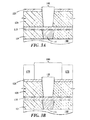
- FIGS. 1A through 1G are cross-sections showing fabrication of a damascene via according to an embodiment of the present invention using a first exemplary dielectric stack
- FIGS. 2A through 2G are cross-sections showing fabrication of a damascene via according to an embodiment of the present invention using a second exemplary dielectric stack;
- FIGS. 3A through 3E are cross-sections showing fabrication of a dual damascene wire according to an embodiment of the present invention using the first exemplary dielectric stack;
- FIGS. 4A through 4E are cross-sections showing fabrication of a dual damascene via according to an embodiment of the present invention using the second exemplary dielectric stack.
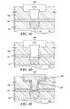
- FIGS. 5A through 5F are cross-sections showing an alternative method of defining a via opening according to an embodiment of the present invention using the second exemplary dielectric stack.
- the embodiments of the present invention utilize a patterned two layer hard mask wherein the patterns in the lower and upper hard mask layers are formed using a reactive ion etch (RIE) process. Openings are then formed in the interlevel dielectric layer under the two layer hard mask using a second RIE which also removes and the upper hard mask layer. The lower hard mask layer is then removed with a wet etch. Further processing completes forming damascene vias or dual damascene wires.
- RIE reactive ion etch
- a photolithographic process is one in which a photoresist layer is applied to a surface of a substrate, the photoresist layer exposed to actinic radiation through a patterned photomask and the exposed photoresist layer developed to form a patterned photoresist layer.
- the photoresist layer comprises positive photoresist
- the developer dissolves the regions of the photoresist exposed to the actinic radiation and does not dissolve the regions where the patterned photomask blocked (or greatly attenuated the intensity of the radiation) from impinging on the photoresist layer.
- the photoresist layer comprises negative photoresist
- the developer does not dissolve the regions of the photoresist exposed to the actinic radiation and does dissolve the regions where the patterned photomask blocked (or greatly attenuated the intensity of the radiation) from impinging on the photoresist layer.
- the patterned photoresist is removed.
- the photoresist may also be left in place and removed by the etch process.
- the photoresist layer may optionally be baked at one or more of the following steps: prior to exposure to actinic radiation, between exposure to actinic radiation and development, after development.
- a damascene process is one in which wire trenches or via openings are formed in a dielectric layer, an electrical conductor of sufficient thickness to fill the trenches is formed in the trenches and on a top surface of the dielectric.
- a chemical-mechanical-polish (CMP) process is performed to remove excess conductor from the surface of the dielectric layer and make the surface of the conductor coplanar with the top surface of the dielectric layer to form damascene wires (or damascene vias).
- CMP chemical-mechanical-polish
- a via first dual-damascene process is one in which via openings are formed through the entire thickness of the dielectric layer followed by formation of trenches part of the way through the dielectric layer in any given cross-sectional view.
- a trench first dual-damascene process is one in which trenches are formed part way through the thickness of a dielectric layer followed by formation of vias inside the trenches the rest of the way through the dielectric layer in any given cross-sectional view. All via openings are intersected by integral wire trenches above and by a wire trench below, but not all trenches need intersect a via opening.
- An electrical conductor of sufficient thickness to fill the trenches and via opening is formed on a top surface of the dielectric layer and a CMP process is performed to make the surface of the conductor in the trench coplanar with the top surface of the dielectric layer to form dual-damascene wires having integral vias.
- voids e.g., copper plating voids
- the metal hard mask must be removed prior to metal filling in order allow tapering of the top of the via and trench profiles which results in improved metal filling that minimizes or eliminates voids in the wires, vias and contacts.
- a hard mask comprising metal nitride on the top surfaces of the underlying dielectric layer (especially ultra low K (dielectric constant) dielectric layer) and the formed damascene and dual damascene wires and contacts (especially the conductive liners).
- An ultra low K (ULK) dielectric material has a K value of 2.7 or less. Therefore, the embodiments of the present invention use a metal oxide or metal oxynitride hard mask layer under the metal nitride hardmask layer.
- the metal oxide or metal oxynitride hard mask layer is removed using a dilute hydrofluoric (HF) acid wet etch etchant.
- the wet etchant comprises a solution of 500 to 1700 parts H 2 O to 1 part of 49% HF by volume (wherein the 49% HF is 49% HF by weight in H 2 O).
- the wet etchant comprises a solution of 1300 to 1500 parts H 2 O to 1 part of 49% HF by volume (wherein the 49% HF is 49% HF by weight in H 2 O).
- the wet etchant comprises a mixture of a solution of 1000 to 1500 parts H 2 O to 1 part of 49% HF by volume (wherein the 49% HF is 49% HF by weight in H 2 O) and citric acid at a temperature between about 22° C. and about 70° C. preferred and between about 50° C. and 70° C. more preferred, thus improving the via or wire/via edge profiles, allowing improved metal fill and increased reliability.
- FIGS. 1A through 1G are cross-sections showing fabrication of a damascene via according to an embodiment of the present invention using a first exemplary dielectric stack.
- a dielectric layer 105 including a damascene conductor 110 is formed on a semiconductor substrate 100 .
- damascene conductors include electrically conductive contacts, electrically conductive vias and electrically conductive wires.
- a damascene conductor is defined as an electrically conductive structure embedded in a dielectric layer wherein a top surface of the damascene conductor is coplanar with the top surface of the dielectric layer it is embedded in. Damascene conductors (i.e., wires, vias and contacts) are formed using the damascene processes described supra.
- the top surfaces of dielectric layer 105 and damascene conductor 110 are coplanar. Formed on the top surfaces of dielectric layer 105 and damascene conductor 110 is a dielectric barrier layer 115 . Formed on a top surface of dielectric barrier layer 115 is an interlevel dielectric layer (ILD) 120 . Formed on a top surface of ILD layer 120 is a dielectric capping layer 125 . Formed on a top surface of dielectric capping layer 125 is a hard mask layer 130 comprising a lower hard mask layer 135 formed on the top surface of dielectric capping layer 125 and an upper hard mask layer 140 formed on a top surface of lower hard mask layer 135 .
- ILD interlevel dielectric layer
- damascene conductor 110 comprises tungsten or copper or copper and a metal nitride.
- dielectric barrier layer 115 is NBLok (SiC(N,H)). In one example, dielectric barrier layer 115 is about 10 nm to about 30 nm thick. In one example, dielectric barrier layer 115 is a diffusion barrier to copper. In one example, ILD layer 120 is a ULK material.
- ULK examples include but are not limited to porous hydrogen silsesquioxane polymer (HSQ), porous methyl silsesquioxane polymer (MSQ), porous (methyl doped silica or SiO x (CH 3 ) y or SiC x O y H y or SiOCH), octametylcyclotetrailoxane (OMCTS) based materials and tetrametylcyclotetrailoxane (TMCTS) based materials.
- ILD layer 120 is about 80 nm to 120 nm thick.
- dielectric capping layer 125 is tetraethylorthosilicate (TEOS).
- dielectric capping layer 125 has a thickness between about 10 nm and about 40 nm. In one example, dielectric capping layer 125 has a thickness between about 10 nm and about 20 nm.
- lower hard mask layer 135 is a metal oxide or metal oxynitride. In one example, lower hard mask layer 135 is titanium oxide or titanium oxynitride. In one example, lower hard mask layer 135 is between about 10 nm and about 20 nm thick.
- upper hard mask layer 140 is a metal nitride. In one example, upper hard mask layer 140 is titanium nitride. In one example, upper hard mask layer 140 is between about 10 nm and about 20 nm thick. It is important that lower hard mask layer 135 be etchable by a wet etch process.
- a patterned photoresist layer 145 having an opening 150 is formed on the top surface of upper hard mask layer 140 .
- opening has a width W 1 of about 20 nm to about 60 nm.
- a first RIE is performed which forms a via opening 155 through opening 150 in hard mask 130 .
- Dielectric capping layer 125 is exposed in the bottom of via opening 155 .
- the first RIE process is selective to upper and lower hard mask layers 140 and 135 over dielectric capping layer 125 .
- the terminology “selective to A over B” is defined as A is etched preferentially relative to B. In one example, there is little etching (i.e., about 10% thickness loss or less) to no etching of dielectric capping layer 125 by the first RIE.
- the first RIE may remove some of patterned photoresist layer 145 .
- a second RIE is performed to extend via opening 155 through dielectric capping layer 125 and ILD layer 120 .
- Dielectric barrier layer 115 is exposed in the bottom of via opening 155 .
- the second RIE process is selective to upper hard mask layer 140 , dielectric capping layer 125 and ILD layer 120 over dielectric barrier layer 115 and lower hard mask layer 135 .
- there is little etching i.e., about 10% thickness loss or less
- the second RIE also removes all remaining patterned photoresist layer 145 and all of remaining upper hard mask layer 140 (see FIG. 1C ).
- a wet etch is performed to remove lower hard mask layer 135 (see FIG. 1D ).
- the wet etch is selective to lower hard mask layer 135 over dielectric capping layer 125 , ILD layer 120 and dielectric barrier layer 115 .
- the wet etch comprises a solution of 500 to 1700 parts H 2 O to 1 part of 49% HF by volume (wherein the 49% HF is 49% HF by weight in H 2 O). In one example, the wet etch comprises a solution of 1300 to 1500 parts H 2 O to 1 part of 49% HF by volume (wherein the 49% HF is 49% HF by weight in H 2 O).
- the wet etch comprises a mixture of a solution of 1000 to 1500 parts H 2 O to 1 part of 49% HF by volume (wherein the 49% HF is 49% HF by weight in H 2 O) and citric acid at a temperature between about 22° C. and about 70° C. preferred and between about 50° C. and 70° C. more preferred.
- a third RIE is performed to extend via opening 155 through dielectric barrier layer 115 .
- Damascene conductor 110 is exposed in the bottom of via opening 155 .
- the third RIE process is selective to dielectric barrier layer 115 over damascene conductor 110 , ILD layer 120 and dielectric capping layer 125 .
- the third RIE can improve the via opening profile.
- an electrically conductive via 160 is formed in (and completely filling) via opening 155 (see FIG. 1F ) using a damascene/CMP process described supra.
- Via 160 includes an electrically conductive liner 165 and a core conductor 170 .
- liner 165 comprises a layer of tantalum on the core conductor and a layer of tantalum nitride on the tantalum layer.
- core conductor 170 comprises copper.
- an additional RIE may be performed between FIGS. 1F and 1G to etch back any dielectric capping layer 125 that may extend into via opening 155 due to undercut of ILD layer 120 by the various RIE etch steps.
- This will produce a via opening profile that will further improve the liner formation and core fill processes and further improve electromigration reliability by removing sharp corners.
- FIGS. 2A through 2G are cross-sections showing fabrication of a damascene via according to an embodiment of the present invention using a second exemplary dielectric stack.
- FIGS. 2A through 2G are similar to respective FIGS. 1A through 1G except there is no dielectric capping layer 125 (see FIG. 1A ).
- dielectric layer 105 including damascene conductor 110 .
- the top surfaces of dielectric layer 105 and damascene conductor 110 are coplanar.
- dielectric barrier layer 115 Formed on the top surfaces of dielectric layer 105 and damascene conductor 110 is dielectric barrier layer 115 .
- ILD interlevel dielectric layer
- a hard mask layer 130 Formed on a top surface of ILD layer 120 is a hard mask layer 130 comprising a lower hard mask layer 135 formed on the top surface of ILD layer 120 and an upper hard mask layer 140 formed on a top surface of lower hard mask layer 135 . Materials and thicknesses of the various layers has been described supra with respect to FIG. 1A .
- a patterned photoresist layer 145 having an opening 150 is formed on the top surface of upper hard mask layer 140 .
- opening has a width W 1 .
- W 1 is between about 20 nm and about 60 nm. In one example, W 1 is between about 10 nm and about 40 nm.
- the first RIE is performed which forms a via opening 155 through opening 150 in hard mask 130 .
- ILD layer 120 is exposed in the bottom of via opening 155 A.
- the first RIE process is selective to upper and lower hard mask layers 140 and 135 over ILD layer 120 . In one example, there is little etching (i.e., about 10% thickness loss or less) to no etching of ILD layer 120 by the first RIE.
- the first RIE may remove some of patterned photoresist layer 145 .
- a second RIE is performed to extend via opening 155 A through ILD layer 120 .
- Dielectric barrier layer 115 is exposed in the bottom of via opening 155 A.
- the second RIE process is selective to upper hard mask layer 140 and ILD layer 120 over dielectric barrier layer 115 and lower hard mask layer 135 .
- there is little etching i.e., about 10% thickness loss or less
- there is little etching i.e., about 10% thickness loss or less
- there is little etching i.e., about 10% thickness loss or less
- the second RIE also removes all remaining patterned photoresist layer 145 and all of remaining upper hard mask layer 140 (see FIG. 2C ).
- a wet etch is performed to remove lower hard mask layer 135 (see FIG. 1D ).
- the wet etch is selective to lower hard mask layer 135 over ILD layer 120 and dielectric barrier layer 115 .
- the wet etch comprises a solution of 500 to 1700 parts H 2 O to 1 part of 49% HF by volume (wherein the 49% HF is 49% HF by weight in H 2 O). In one example, the wet etch comprises a solution of 1300 to 1500 parts H 2 O to 1 part of 49% HF by volume (wherein the 49% HF is 49% HF by weight in H 2 O). In one example, the wet etch comprises a mixture of a solution of 1000 to 1500 parts H 2 O to 1 part of 49% HF by volume (wherein the 49% HF is 49% HF by weight in H 2 O) and citric acid at a temperature between about 22° C. and about 70° C. preferred and between about 50° C. and 70° C. more preferred.
- a third RIE is performed to extend via opening 155 A through dielectric barrier layer 115 .
- Damascene conductor 110 is exposed in the bottom of via opening 155 A.
- the third RIE process is selective to dielectric barrier layer 115 over damascene conductor 110 and ILD layer 120 . In one example, there is little etching (i.e., about 10% thickness loss or less) to no etching of damascene conductor 110 by the third RIE.
- electrically conductive via 160 is formed in (and completely filling) via opening 155 A (see FIG. 2F ) using a damascene/CMP process described supra. Via 160 has been described supra with respect to FIG. 1G .
- FIGS. 3A through 3E are cross-sections showing fabrication of a dual damascene wire according to an embodiment of the present invention using the first exemplary dielectric stack.
- FIG. 3A is the same as FIG. 1E .
- via opening 155 has been formed through dielectric capping layer 125 and ILD layer 120 , but not through dielectric barrier layer 115 . Only the first and second RIEs have been performed.
- a second patterned photoresist layer 175 having a opening 180 is formed on the top surface of dielectric capping layer 125 .
- a third RIE is performed to form a trench 180 extending completely through dielectric capping layer 125 and into but not completely through ILD layer 120 .
- This third RIE process (different from the third RIE of FIG. 1G ) is selective to ILD layer 120 and dielectric capping layer 125 over dielectric barrier layer 115 .
- there is little etching i.e., about 10% thickness loss or less) to no etching of dielectric barrier layer 115 by the third RIE.
- a fourth RIE is performed to extend via opening 155 through dielectric barrier layer 115 . Wire or contact 115 is exposed in the bottom of via opening 155 .
- the fourth RIE process is selective to dielectric barrier layer 115 over damascene conductor 110 , ILD layer 120 and dielectric capping layer 125 . In one example, there is little etching (i.e., about 10% thickness loss or less) to no etching of damascene conductor 110 by the fourth RIE.
- the fourth RIE removes any remaining second patterned photoresist layer 175 .
- a wet or dry (i.e., plasma) process may be used to remove any remaining second patterned photoresist layer 175 .
- Dual damascene wire 185 is formed in (and completely filling) via opening 155 and trench 180 (see FIG. 3D ) using a damascene/CMP process described supra.
- Dual damascene wire includes and electrically conductive liner 190 and a core conductor 195 .
- liner 190 comprises a layer of tantalum on the core conductor and a layer of tantalum nitride on the tantalum layer.
- core conductor 195 comprises copper.
- FIGS. 4A through 4E are cross-sections showing fabrication of a dual damascene via according to an embodiment of the present invention using the second exemplary dielectric stack.
- FIG. 4A is the same as FIG. 2E .
- FIGS. 4A through 4E differs from FIGS. 3A through 3E only in the fact that there is no dielectric capping layer 125 (see FIG. 3A ) in FIGS. 4A through 4E .
- a via opening 155 A has been formed through dielectric capping layer 125 and ILD layer 120 , but not through dielectric barrier layer 115 . Only the first and second RIEs have been performed.
- second patterned photoresist layer 175 having opening 180 is formed on the top surface of ILD layer 120 .
- a third RIE is performed to form a trench 180 extending into but not completely through ILD layer 120 .
- This third RIE process (different from the third RIE of FIG. 2G ) is selective to ILD layer 120 over dielectric barrier layer 115 . In one example, there is little etching (i.e., about 10% thickness loss or less) to no etching of dielectric barrier layer 115 by the third RIE.
- a fourth RIE is performed to extend via opening 155 A through dielectric barrier layer 115 . Wire or contact 115 is exposed in the bottom of via opening 155 A.
- the fourth RIE process is selective to dielectric barrier layer 115 over damascene conductor 110 , ILD layer 120 and dielectric capping layer 125 . In one example, there is little etching (i.e., about 10% thickness loss or less) to no etching of damascene conductor 110 by the fourth RIE.
- the fourth RIE removes any remaining second patterned photoresist layer 175 .
- a wet or dry (i.e., plasma) process may be used to remove any remaining second patterned photoresist layer 175 .
- Dual damascene wire 195 is formed in (and completely filling) via opening 155 A and trench 180 (see FIG. 4D ) using a damascene/CMP process described supra.
- Dual damascene wire 195 includes and electrically conductive liner 200 and a core conductor 205 .
- liner 200 comprises a layer of tantalum on the core conductor and a layer of tantalum nitride on the tantalum layer.
- core conductor 205 comprises copper.
- FIGS. 5A through 5F are cross-sections showing an alternative method of defining a via opening according to an embodiment of the present invention using the second exemplary dielectric stack.
- FIGS. 5A-5E three hardmask layers instead of two are used and the opening in the hardmask layer is defined by a photolithographically formed opening in an additional hardmask layer instead of directly by a photolithographic process as in FIGS. 1C and 2C .
- an additional hardmask layer 210 is form on the top surface of upper hardmask layer 140 of hardmask layer 130 .
- patterned photoresist layer 145 is formed on the top surface of additional hardmask layer 210 .
- an additional RIE is used to form via opening 155 in additional hardmask layer 210 . Additional RIE is selective to additional hardmask layer to upper hardmask layer 140 .
- additional hardmask layer is TEOS.
- additional hardmask layer 210 has a thickness between about 10 nm and about 40 nm. In one example, additional hardmask layer 210 has a thickness between about 10 nm and about 20 nm.
- the additional RIE may remove some of patterned photoresist layer 145 .
- patterned photoresist layer 145 is removed, for example, using a oxygen plasma process.
- the first RIE described supra with respect to FIG. 1C is performed. The first RIE process is selective to upper and lower hard mask layers 140 and 135 over additional hardmask layer 210 and dielectric capping layer 125 .
- etching i.e., about 10% thickness loss or less
- first RIE described supra with respect to FIG. 1D
- the second RIE process is selective to upper hard mask layer 140 , dielectric capping layer 125 and ILD layer 120 over dielectric barrier layer 115 and lower hard mask layer 135 .
- there is little etching i.e., about 10% thickness loss or less to no etching of dielectric barrier layer 115 by the second RIE.
- the embodiments of the present invention provide a method for forming damascene vias and dual damascene wires with reduced damage to the contact or wire the via is contacting in the lower wiring level and improved via dimensional control due to reduced lateral etch of the interlevel dielectric that defines the via profile.
Abstract
Description
Claims (21)
Priority Applications (1)
| Application Number | Priority Date | Filing Date | Title |
|---|---|---|---|
| US13/905,351 US8853095B1 (en) | 2013-05-30 | 2013-05-30 | Hybrid hard mask for damascene and dual damascene |
Applications Claiming Priority (1)
| Application Number | Priority Date | Filing Date | Title |
|---|---|---|---|
| US13/905,351 US8853095B1 (en) | 2013-05-30 | 2013-05-30 | Hybrid hard mask for damascene and dual damascene |
Publications (1)
| Publication Number | Publication Date |
|---|---|
| US8853095B1 true US8853095B1 (en) | 2014-10-07 |
Family
ID=51626917
Family Applications (1)
| Application Number | Title | Priority Date | Filing Date |
|---|---|---|---|
| US13/905,351 Expired - Fee Related US8853095B1 (en) | 2013-05-30 | 2013-05-30 | Hybrid hard mask for damascene and dual damascene |
Country Status (1)
| Country | Link |
|---|---|
| US (1) | US8853095B1 (en) |
Cited By (5)
| Publication number | Priority date | Publication date | Assignee | Title |
|---|---|---|---|---|
| US9123785B1 (en) * | 2014-03-10 | 2015-09-01 | Intermolecular, Inc. | Method to etch Cu/Ta/TaN selectively using dilute aqueous HF/HCI solution |
| US9431343B1 (en) | 2015-03-11 | 2016-08-30 | Samsung Electronics Co., Ltd. | Stacked damascene structures for microelectronic devices |
| US20170076958A1 (en) * | 2015-09-11 | 2017-03-16 | Kabushiki Kaisha Toshiba | Manufacturing method of semiconductor device |
| US11127902B2 (en) * | 2017-01-03 | 2021-09-21 | Samsung Display Co., Ltd. | Organic light-emitting display apparatus and method of manufacturing the same |
| US20220302132A1 (en) * | 2015-12-03 | 2022-09-22 | Taiwan Semiconductor Manufacturing Company, Ltd. | Method for manufacturing static random access memory device |
Citations (23)
| Publication number | Priority date | Publication date | Assignee | Title |
|---|---|---|---|---|
| US4690871A (en) | 1986-03-10 | 1987-09-01 | Gordon Roy G | Protective overcoat of titanium nitride films |
| US5091244A (en) | 1990-08-10 | 1992-02-25 | Viratec Thin Films, Inc. | Electrically-conductive, light-attenuating antireflection coating |
| US5122225A (en) | 1990-11-21 | 1992-06-16 | Texas Instruments Incorporated | Selective etch method |
| US5407733A (en) | 1990-08-10 | 1995-04-18 | Viratec Thin Films, Inc. | Electrically-conductive, light-attenuating antireflection coating |
| US5858184A (en) | 1995-06-07 | 1999-01-12 | Applied Materials, Inc. | Process for forming improved titanium-containing barrier layers |
| US5938898A (en) | 1991-12-26 | 1999-08-17 | Asahi Glass Company Ltd. | Functional product |
| US6399446B1 (en) | 1999-10-29 | 2002-06-04 | Advanced Micro Devices, Inc. | Process for fabricating high density memory cells using a metallic hard mask |
| US6531404B1 (en) | 2000-08-04 | 2003-03-11 | Applied Materials Inc. | Method of etching titanium nitride |
| US6534809B2 (en) | 1999-12-22 | 2003-03-18 | Agilent Technologies, Inc. | Hardmask designs for dry etching FeRAM capacitor stacks |
| US20040142565A1 (en) * | 2003-01-21 | 2004-07-22 | Cooney Edward C. | Single and multilevel rework |
| US6809033B1 (en) | 2001-11-07 | 2004-10-26 | Fasl, Llc | Innovative method of hard mask removal |
| US6828161B2 (en) | 2001-12-31 | 2004-12-07 | Texas Instruments Incorporated | Method of forming an FeRAM having a multi-layer hard mask and patterning thereof |
| US7045070B1 (en) | 1997-07-03 | 2006-05-16 | Infineon Technologies Ag | Method of producing an electrode configuration and method of electrically contacting the electrode configuration |
| US20080244896A1 (en) * | 2007-03-20 | 2008-10-09 | Hitachi Global Storage Technologies | Additive gap process to define trailing and side shield gap for a perpendicular write head |
| US20090131295A1 (en) * | 2007-11-16 | 2009-05-21 | Hua Cui | Compositions for Removal of Metal Hard Mask Etching Residues from a Semiconductor Substrate |
| US7687381B2 (en) * | 2008-03-19 | 2010-03-30 | Samsung Electronics Co., Ltd. | Method of forming electrical interconnects within insulating layers that form consecutive sidewalls including forming a reaction layer on the inner sidewall |
| US7922824B2 (en) | 2005-10-05 | 2011-04-12 | Advanced Technology Materials, Inc. | Oxidizing aqueous cleaner for the removal of post-etch residues |
| US7981777B1 (en) | 2007-02-22 | 2011-07-19 | Novellus Systems, Inc. | Methods of depositing stable and hermetic ashable hardmask films |
| US20120028373A1 (en) * | 2010-07-30 | 2012-02-02 | Magic Technologies, Inc. | Bi-layer hard mask for the patterning and etching of nanometer size MRAM devices |
| US20120104622A1 (en) * | 2010-10-27 | 2012-05-03 | Kim Sunoo | Through Level Vias and Methods of Formation Thereof |
| US8293625B2 (en) * | 2011-01-19 | 2012-10-23 | International Business Machines Corporation | Structure and method for hard mask removal on an SOI substrate without using CMP process |
| US20120286231A1 (en) * | 2010-01-21 | 2012-11-15 | Nec Corporation | Semiconductor device and method of manufacturing the same |
| US20130005147A1 (en) * | 2011-06-28 | 2013-01-03 | International Business Machines Corporation | Method of reducing critical dimension process bias differences between narrow and wide damascene wires |
-
2013
- 2013-05-30 US US13/905,351 patent/US8853095B1/en not_active Expired - Fee Related
Patent Citations (23)
| Publication number | Priority date | Publication date | Assignee | Title |
|---|---|---|---|---|
| US4690871A (en) | 1986-03-10 | 1987-09-01 | Gordon Roy G | Protective overcoat of titanium nitride films |
| US5091244A (en) | 1990-08-10 | 1992-02-25 | Viratec Thin Films, Inc. | Electrically-conductive, light-attenuating antireflection coating |
| US5407733A (en) | 1990-08-10 | 1995-04-18 | Viratec Thin Films, Inc. | Electrically-conductive, light-attenuating antireflection coating |
| US5122225A (en) | 1990-11-21 | 1992-06-16 | Texas Instruments Incorporated | Selective etch method |
| US5938898A (en) | 1991-12-26 | 1999-08-17 | Asahi Glass Company Ltd. | Functional product |
| US5858184A (en) | 1995-06-07 | 1999-01-12 | Applied Materials, Inc. | Process for forming improved titanium-containing barrier layers |
| US7045070B1 (en) | 1997-07-03 | 2006-05-16 | Infineon Technologies Ag | Method of producing an electrode configuration and method of electrically contacting the electrode configuration |
| US6399446B1 (en) | 1999-10-29 | 2002-06-04 | Advanced Micro Devices, Inc. | Process for fabricating high density memory cells using a metallic hard mask |
| US6534809B2 (en) | 1999-12-22 | 2003-03-18 | Agilent Technologies, Inc. | Hardmask designs for dry etching FeRAM capacitor stacks |
| US6531404B1 (en) | 2000-08-04 | 2003-03-11 | Applied Materials Inc. | Method of etching titanium nitride |
| US6809033B1 (en) | 2001-11-07 | 2004-10-26 | Fasl, Llc | Innovative method of hard mask removal |
| US6828161B2 (en) | 2001-12-31 | 2004-12-07 | Texas Instruments Incorporated | Method of forming an FeRAM having a multi-layer hard mask and patterning thereof |
| US20040142565A1 (en) * | 2003-01-21 | 2004-07-22 | Cooney Edward C. | Single and multilevel rework |
| US7922824B2 (en) | 2005-10-05 | 2011-04-12 | Advanced Technology Materials, Inc. | Oxidizing aqueous cleaner for the removal of post-etch residues |
| US7981777B1 (en) | 2007-02-22 | 2011-07-19 | Novellus Systems, Inc. | Methods of depositing stable and hermetic ashable hardmask films |
| US20080244896A1 (en) * | 2007-03-20 | 2008-10-09 | Hitachi Global Storage Technologies | Additive gap process to define trailing and side shield gap for a perpendicular write head |
| US20090131295A1 (en) * | 2007-11-16 | 2009-05-21 | Hua Cui | Compositions for Removal of Metal Hard Mask Etching Residues from a Semiconductor Substrate |
| US7687381B2 (en) * | 2008-03-19 | 2010-03-30 | Samsung Electronics Co., Ltd. | Method of forming electrical interconnects within insulating layers that form consecutive sidewalls including forming a reaction layer on the inner sidewall |
| US20120286231A1 (en) * | 2010-01-21 | 2012-11-15 | Nec Corporation | Semiconductor device and method of manufacturing the same |
| US20120028373A1 (en) * | 2010-07-30 | 2012-02-02 | Magic Technologies, Inc. | Bi-layer hard mask for the patterning and etching of nanometer size MRAM devices |
| US20120104622A1 (en) * | 2010-10-27 | 2012-05-03 | Kim Sunoo | Through Level Vias and Methods of Formation Thereof |
| US8293625B2 (en) * | 2011-01-19 | 2012-10-23 | International Business Machines Corporation | Structure and method for hard mask removal on an SOI substrate without using CMP process |
| US20130005147A1 (en) * | 2011-06-28 | 2013-01-03 | International Business Machines Corporation | Method of reducing critical dimension process bias differences between narrow and wide damascene wires |
Non-Patent Citations (4)
| Title |
|---|
| Tang, T.E. et al., "Titanium Nitride Local Interconnect Technology for VLSI" IEEE Transactions on Electron Devices (Mar. 1987) pp. 682-688, vol. ED-34, No. 3. |
| Tompkins, H.G. et al. "Oxidation of TiN in an Oxygen Plasma Asher" Journal of Vacuum Science & Technology A: Vacuum, Surfaces, and Films (Jul./Aug. 1994) pp. 2446-2450, vol. 12, No. 4. |
| U.S. Appl. No. 13/741,611 Title: Lithographic Material Stack Including a Metal-Compound Hard Mask filed Jan. 15, 2013 Inventor(s): Daniel C. Edelstein. |
| U.S. Appl. No. 13/741,638 Title: Titanium Oxynitride Hard Mask for Lithographic Patterning filed Jan. 15, 2013 Inventor(s): Son V. Nguyen, et al. |
Cited By (7)
| Publication number | Priority date | Publication date | Assignee | Title |
|---|---|---|---|---|
| US9123785B1 (en) * | 2014-03-10 | 2015-09-01 | Intermolecular, Inc. | Method to etch Cu/Ta/TaN selectively using dilute aqueous HF/HCI solution |
| US9431343B1 (en) | 2015-03-11 | 2016-08-30 | Samsung Electronics Co., Ltd. | Stacked damascene structures for microelectronic devices |
| US20170076958A1 (en) * | 2015-09-11 | 2017-03-16 | Kabushiki Kaisha Toshiba | Manufacturing method of semiconductor device |
| CN106531687A (en) * | 2015-09-11 | 2017-03-22 | 株式会社东芝 | Manufacturing method of semiconductor device |
| US20220302132A1 (en) * | 2015-12-03 | 2022-09-22 | Taiwan Semiconductor Manufacturing Company, Ltd. | Method for manufacturing static random access memory device |
| US11832431B2 (en) * | 2015-12-03 | 2023-11-28 | Taiwan Semiconductor Manufacturing Company, Ltd. | Method for manufacturing static random access memory device |
| US11127902B2 (en) * | 2017-01-03 | 2021-09-21 | Samsung Display Co., Ltd. | Organic light-emitting display apparatus and method of manufacturing the same |
Similar Documents
| Publication | Publication Date | Title |
|---|---|---|
| US10607933B2 (en) | Interconnect structures with fully aligned vias | |
| US7601607B2 (en) | Protruded contact and insertion of inter-layer-dielectric material to match damascene hardmask to improve undercut for low-k interconnects | |
| JP4571785B2 (en) | Manufacturing method of semiconductor device | |
| US8450212B2 (en) | Method of reducing critical dimension process bias differences between narrow and wide damascene wires | |
| US7470616B1 (en) | Damascene wiring fabrication methods incorporating dielectric cap etch process with hard mask retention | |
| CN107731739B (en) | Method for forming semiconductor structure | |
| CN108074861B (en) | Semiconductor structure and manufacturing method thereof | |
| US8853095B1 (en) | Hybrid hard mask for damascene and dual damascene | |
| US20080174018A1 (en) | Semiconductor device and method for fabricating the same | |
| US20090087992A1 (en) | Method of minimizing via sidewall damages during dual damascene trench reactive ion etching in a via first scheme | |
| TW201608688A (en) | Semiconductor device structure and method for forming the same | |
| TW202145392A (en) | Semiconductor structure | |
| WO2008151166A1 (en) | Damascene process having retained capping layer through metallization for protecting low-k dielectrics | |
| US8835306B2 (en) | Methods for fabricating integrated circuits having embedded electrical interconnects | |
| US8293638B2 (en) | Method of fabricating damascene structures | |
| US20120199980A1 (en) | Integrated circuits having interconnect structures and methods for fabricating integrated circuits having interconnect structures | |
| JP5047504B2 (en) | Method for manufacturing dual damascene wiring of semiconductor device using via capping protective film | |
| US20130161798A1 (en) | Graded density layer for formation of interconnect structures | |
| US7192877B2 (en) | Low-K dielectric etch process for dual-damascene structures | |
| US20230011792A1 (en) | Self-Aligned Interconnect Structure And Method Of Forming The Same | |
| JP2008282852A (en) | Process for fabricating semiconductor device | |
| US9018097B2 (en) | Semiconductor device processing with reduced wiring puddle formation | |
| CN111293074B (en) | Semiconductor structure and forming method thereof | |
| US6875688B1 (en) | Method for reactive ion etch processing of a dual damascene structure | |
| JP2005005697A (en) | Manufacturing method of semiconductor device |
Legal Events
| Date | Code | Title | Description |
|---|---|---|---|
| AS | Assignment |
Owner name: INTERNATIONAL BUSINESS MACHINES CORPORATION, NEW Y Free format text: ASSIGNMENT OF ASSIGNORS INTEREST;ASSIGNORS:KELLY, JAMES J;VO, TUAN ANH;SIGNING DATES FROM 20130424 TO 20130524;REEL/FRAME:030512/0055 |
|
| AS | Assignment |
Owner name: GLOBALFOUNDRIES U.S. 2 LLC, NEW YORK Free format text: ASSIGNMENT OF ASSIGNORS INTEREST;ASSIGNOR:INTERNATIONAL BUSINESS MACHINES CORPORATION;REEL/FRAME:036550/0001 Effective date: 20150629 |
|
| AS | Assignment |
Owner name: GLOBALFOUNDRIES INC., CAYMAN ISLANDS Free format text: ASSIGNMENT OF ASSIGNORS INTEREST;ASSIGNORS:GLOBALFOUNDRIES U.S. 2 LLC;GLOBALFOUNDRIES U.S. INC.;REEL/FRAME:036779/0001 Effective date: 20150910 |
|
| FEPP | Fee payment procedure |
Free format text: MAINTENANCE FEE REMINDER MAILED (ORIGINAL EVENT CODE: REM.) |
|
| LAPS | Lapse for failure to pay maintenance fees |
Free format text: PATENT EXPIRED FOR FAILURE TO PAY MAINTENANCE FEES (ORIGINAL EVENT CODE: EXP.); ENTITY STATUS OF PATENT OWNER: LARGE ENTITY |
|
| STCH | Information on status: patent discontinuation |
Free format text: PATENT EXPIRED DUE TO NONPAYMENT OF MAINTENANCE FEES UNDER 37 CFR 1.362 |
|
| AS | Assignment |
Owner name: WILMINGTON TRUST, NATIONAL ASSOCIATION, DELAWARE Free format text: SECURITY AGREEMENT;ASSIGNOR:GLOBALFOUNDRIES INC.;REEL/FRAME:049490/0001 Effective date: 20181127 |
|
| FP | Lapsed due to failure to pay maintenance fee |
Effective date: 20181007 |
|
| AS | Assignment |
Owner name: GLOBALFOUNDRIES INC., CAYMAN ISLANDS Free format text: RELEASE BY SECURED PARTY;ASSIGNOR:WILMINGTON TRUST, NATIONAL ASSOCIATION;REEL/FRAME:054636/0001 Effective date: 20201117 |
|
| AS | Assignment |
Owner name: GLOBALFOUNDRIES U.S. INC., NEW YORK Free format text: RELEASE BY SECURED PARTY;ASSIGNOR:WILMINGTON TRUST, NATIONAL ASSOCIATION;REEL/FRAME:056987/0001 Effective date: 20201117 |