US8854620B2 - Curved grating spectrometer and wavelength multiplexer or demultiplexer with very high wavelength resolution - Google Patents
Curved grating spectrometer and wavelength multiplexer or demultiplexer with very high wavelength resolution Download PDFInfo
- Publication number
- US8854620B2 US8854620B2 US13/911,847 US201313911847A US8854620B2 US 8854620 B2 US8854620 B2 US 8854620B2 US 201313911847 A US201313911847 A US 201313911847A US 8854620 B2 US8854620 B2 US 8854620B2
- Authority
- US
- United States
- Prior art keywords
- slit
- grating
- wavelength
- output
- demultiplexer
- Prior art date
- Legal status (The legal status is an assumption and is not a legal conclusion. Google has not performed a legal analysis and makes no representation as to the accuracy of the status listed.)
- Expired - Lifetime
Links
- 230000003287 optical effect Effects 0.000 claims description 37
- 238000001228 spectrum Methods 0.000 claims description 3
- 239000000203 mixture Substances 0.000 claims description 2
- 230000023077 detection of light stimulus Effects 0.000 claims 1
- 238000013461 design Methods 0.000 abstract description 46
- 238000000034 method Methods 0.000 abstract description 12
- 230000001419 dependent effect Effects 0.000 abstract description 3
- 239000013598 vector Substances 0.000 description 19
- 230000004075 alteration Effects 0.000 description 8
- VYPSYNLAJGMNEJ-UHFFFAOYSA-N Silicium dioxide Chemical compound O=[Si]=O VYPSYNLAJGMNEJ-UHFFFAOYSA-N 0.000 description 6
- 239000004065 semiconductor Substances 0.000 description 6
- 239000006185 dispersion Substances 0.000 description 5
- 238000003384 imaging method Methods 0.000 description 5
- 239000000463 material Substances 0.000 description 5
- 230000010354 integration Effects 0.000 description 4
- 238000006073 displacement reaction Methods 0.000 description 3
- 230000005684 electric field Effects 0.000 description 3
- 238000004519 manufacturing process Methods 0.000 description 3
- 230000001902 propagating effect Effects 0.000 description 3
- 239000000377 silicon dioxide Substances 0.000 description 3
- 102100025490 Slit homolog 1 protein Human genes 0.000 description 2
- 101710123186 Slit homolog 1 protein Proteins 0.000 description 2
- 102100027340 Slit homolog 2 protein Human genes 0.000 description 2
- 101710133576 Slit homolog 2 protein Proteins 0.000 description 2
- 238000004364 calculation method Methods 0.000 description 2
- 238000005516 engineering process Methods 0.000 description 2
- 239000010410 layer Substances 0.000 description 2
- 239000013307 optical fiber Substances 0.000 description 2
- 229910052710 silicon Inorganic materials 0.000 description 2
- 239000010703 silicon Substances 0.000 description 2
- 238000004088 simulation Methods 0.000 description 2
- 239000000758 substrate Substances 0.000 description 2
- 229910001218 Gallium arsenide Inorganic materials 0.000 description 1
- 238000004458 analytical method Methods 0.000 description 1
- 238000000137 annealing Methods 0.000 description 1
- 238000004891 communication Methods 0.000 description 1
- 150000001875 compounds Chemical class 0.000 description 1
- 238000012937 correction Methods 0.000 description 1
- 230000003247 decreasing effect Effects 0.000 description 1
- 230000007547 defect Effects 0.000 description 1
- 238000010586 diagram Methods 0.000 description 1
- 229910003460 diamond Inorganic materials 0.000 description 1
- 239000010432 diamond Substances 0.000 description 1
- 239000003989 dielectric material Substances 0.000 description 1
- 238000009792 diffusion process Methods 0.000 description 1
- 239000011521 glass Substances 0.000 description 1
- PCHJSUWPFVWCPO-UHFFFAOYSA-N gold Chemical compound [Au] PCHJSUWPFVWCPO-UHFFFAOYSA-N 0.000 description 1
- 239000010931 gold Substances 0.000 description 1
- 229910052737 gold Inorganic materials 0.000 description 1
- 238000012986 modification Methods 0.000 description 1
- 230000004048 modification Effects 0.000 description 1
- 239000002365 multiple layer Substances 0.000 description 1
- 230000005693 optoelectronics Effects 0.000 description 1
- 229920000642 polymer Polymers 0.000 description 1
- 238000010183 spectrum analysis Methods 0.000 description 1
- 238000006467 substitution reaction Methods 0.000 description 1
- 230000002123 temporal effect Effects 0.000 description 1
Images


Classifications
-
- H—ELECTRICITY
- H04—ELECTRIC COMMUNICATION TECHNIQUE
- H04B—TRANSMISSION
- H04B10/00—Transmission systems employing electromagnetic waves other than radio-waves, e.g. infrared, visible or ultraviolet light, or employing corpuscular radiation, e.g. quantum communication
- H04B10/07—Arrangements for monitoring or testing transmission systems; Arrangements for fault measurement of transmission systems
-
- G—PHYSICS
- G01—MEASURING; TESTING
- G01J—MEASUREMENT OF INTENSITY, VELOCITY, SPECTRAL CONTENT, POLARISATION, PHASE OR PULSE CHARACTERISTICS OF INFRARED, VISIBLE OR ULTRAVIOLET LIGHT; COLORIMETRY; RADIATION PYROMETRY
- G01J3/00—Spectrometry; Spectrophotometry; Monochromators; Measuring colours
- G01J3/02—Details
- G01J3/0256—Compact construction
-
- G—PHYSICS
- G01—MEASURING; TESTING
- G01J—MEASUREMENT OF INTENSITY, VELOCITY, SPECTRAL CONTENT, POLARISATION, PHASE OR PULSE CHARACTERISTICS OF INFRARED, VISIBLE OR ULTRAVIOLET LIGHT; COLORIMETRY; RADIATION PYROMETRY
- G01J3/00—Spectrometry; Spectrophotometry; Monochromators; Measuring colours
- G01J3/12—Generating the spectrum; Monochromators
- G01J3/18—Generating the spectrum; Monochromators using diffraction elements, e.g. grating
- G01J3/20—Rowland circle spectrometers
-
- G—PHYSICS
- G01—MEASURING; TESTING
- G01J—MEASUREMENT OF INTENSITY, VELOCITY, SPECTRAL CONTENT, POLARISATION, PHASE OR PULSE CHARACTERISTICS OF INFRARED, VISIBLE OR ULTRAVIOLET LIGHT; COLORIMETRY; RADIATION PYROMETRY
- G01J3/00—Spectrometry; Spectrophotometry; Monochromators; Measuring colours
- G01J3/12—Generating the spectrum; Monochromators
- G01J3/18—Generating the spectrum; Monochromators using diffraction elements, e.g. grating
- G01J3/22—Littrow mirror spectrometers
-
- G—PHYSICS
- G02—OPTICS
- G02B—OPTICAL ELEMENTS, SYSTEMS OR APPARATUS
- G02B6/00—Light guides; Structural details of arrangements comprising light guides and other optical elements, e.g. couplings
- G02B6/24—Coupling light guides
- G02B6/26—Optical coupling means
- G02B6/28—Optical coupling means having data bus means, i.e. plural waveguides interconnected and providing an inherently bidirectional system by mixing and splitting signals
- G02B6/293—Optical coupling means having data bus means, i.e. plural waveguides interconnected and providing an inherently bidirectional system by mixing and splitting signals with wavelength selective means
- G02B6/29304—Optical coupling means having data bus means, i.e. plural waveguides interconnected and providing an inherently bidirectional system by mixing and splitting signals with wavelength selective means operating by diffraction, e.g. grating
- G02B6/29316—Light guides comprising a diffractive element, e.g. grating in or on the light guide such that diffracted light is confined in the light guide
- G02B6/29325—Light guides comprising a diffractive element, e.g. grating in or on the light guide such that diffracted light is confined in the light guide of the slab or planar or plate like form, i.e. confinement in a single transverse dimension only
- G02B6/29326—Diffractive elements having focusing properties, e.g. curved gratings
-
- G—PHYSICS
- G02—OPTICS
- G02B—OPTICAL ELEMENTS, SYSTEMS OR APPARATUS
- G02B6/00—Light guides; Structural details of arrangements comprising light guides and other optical elements, e.g. couplings
- G02B6/24—Coupling light guides
- G02B6/26—Optical coupling means
- G02B6/28—Optical coupling means having data bus means, i.e. plural waveguides interconnected and providing an inherently bidirectional system by mixing and splitting signals
- G02B6/293—Optical coupling means having data bus means, i.e. plural waveguides interconnected and providing an inherently bidirectional system by mixing and splitting signals with wavelength selective means
- G02B6/29304—Optical coupling means having data bus means, i.e. plural waveguides interconnected and providing an inherently bidirectional system by mixing and splitting signals with wavelength selective means operating by diffraction, e.g. grating
- G02B6/29316—Light guides comprising a diffractive element, e.g. grating in or on the light guide such that diffracted light is confined in the light guide
- G02B6/29325—Light guides comprising a diffractive element, e.g. grating in or on the light guide such that diffracted light is confined in the light guide of the slab or planar or plate like form, i.e. confinement in a single transverse dimension only
- G02B6/29328—Diffractive elements operating in reflection
Definitions
- the present invention relates to semiconductor photonic and opto-electronic devices.
- the present invention relates to an integrated optical wavelength multiplexers and demultiplexers and method of making the same.
- Optical gratings are well known in the art and are used to disperse optical spectra spatially. Such gratings are commonly used in optical spectrometers to analyze the spectra composition of an optical beam. There is always a trade off between the length of an optical spectrometer and its resolution. Thus, if a higher wavelength resolution is required, the length required is also longer.
- RS the relative resolution vs size
- RS basically measures the compactness of a spectrometer for a given resolution power. The smaller the RS value, the more compact is the spectrometer. Only a few conventional spectrometers have RS factor less than about 10. This is primarily because of the various limitations in the current art (as will be described below).
- FIG. 1A The schematics of such a grating spectrometer is shown in FIG. 1A , illustrating an optical beam 1 entering an entrance slit 2 with slit size w 1 .
- the beam after slit 2 , undergoes wave diffraction towards a curved grating 3 , which diffracts the beam spatially in a direction that is dependent on the optical wavelength of the beam.
- the curvature of the grating helps to refocus the diffracted beam to an exit slit 4 with slit size w 2 .
- exit slit is also referred to as “outout slit” below so that the terms “exit slit” and “output slit” will be used totally interchangeably.
- the terms “entrance slit” and “input slit” will be used totally interchangeably/Light through slit 4 is then detected by a photo detector 5 .
- the commonly used design for the curved grating 3 is the Rowland design. In the Rowland design, the grating has a circularly curved shape of radius R 6 and the slits SL 1 and SL 2 lie in a circle of radius R/2 7 as shown in FIG. 1A .
- the grating is ruled using a diamond tip with constant horizontal displacement d, which ruled the curved surface with constant Chord lines C 1 , C 2 , C 3 and so forth, as shown in FIG. 1B .
- the segment lengths, S 1 , S 2 , S 3 and so forth, along the curved surface are not a constant and vary along the curved surface.
- ⁇ div (defined by the angle of beam propagation at full-width half maximum (FWHM) of the beam intensity)
- FWHM full-width half maximum
- ⁇ div 2 ⁇ /d (in Radian).
- length L be the distance between the grating center and entrance slit 1 , which is also approximately the distance between the grating center and the exit slit 4 .
- the resolution of the spectrometer increases with decreasing slit size w 2 .
- the imaging through the curved grating requires w 1 and w 2 to be about equal.
- a smaller slit size w 1 leads to a larger diffraction angle ⁇ div . It can be shown that the Rowland design works reasonably well up to ⁇ div ⁇ 4°. When ⁇ div >4°, the Rowland design could not give a sharp enough focus at the exit slit 4 (for ⁇ 0.1 nm), thereby limiting the size of w 2 and hence the resolution of the spectrometer.
- FIG. 1C illustrating the ray tracing for the typical Rolwand-Echelle design at 4, 8, and 16 DEG diffraction.
- the ray tracing will allow us to see potential focusing distortion or aberration at the exit slit.
- a curved-grating spectrometer is well specified by geometric configurations of its components as shown in FIG. 2 .
- the center of the grating refers to the part of the grating hit by the center, i.e. high intensity point, of the entrance beam.
- and d ⁇ 1
- a circle can be defined by these three points X 0 , X 1 , and X 2 and its radius is referred to as the radius of curvature at the grating center.
- the location of the exit slit i.e.
- the location of the detector this is specified by an angle ⁇ 2 with respect to the normal of the grating center and the distance S 2 from the grating center.
- the initial groove spacing d is usually chosen to satisfy the diffraction grating formula for a given entrance slit and detector location.
- the locus of all the grooves defined by the line that joins all tips of the vectors X ( ⁇ N) , . . . , X ( ⁇ 1) , X 0 , X 1 , . . . , X N form a curved shape, which can lie in a circle or in any other curvilinear line. Curved shape of the grating acts as an imaging element of the spectrometer.
- each groove centered at X i is not critical to the resolution power of the grating and hence is not necessary to be a part of the main specification.
- the groove shape is related to the diffraction efficiency.
- it is typically made a planar surface for each groove, oriented in such a way that it acts like a tiny mirror reflecting the input ray towards the angle ⁇ 2 , a process typically referred to as blazing to angle ⁇ 2 (for a given wavelength ⁇ ).
- a section of each groove which reflects light is physically a two-dimensional surface of a particular shape, not a one-dimensional curve.
- the geometric shape of a groove is usually referred to as a one-dimensional curve of a particular shape. This is because there is no variation in the grating shape in the direction perpendicular to the plane where grating lies.
- spectrometers within a planar waveguide are strictly two-dimensional in their nature and the shape of grating or grooves will be referred with a curve, not with surface.
- the entrance slit SL 1 is located on a circle of R/2, where R is the radius of curvature of the grating at the grating center. This curvature at the grating center is called the grating-center curve. This circle of radius R/2 is called the Rowland circle and it is tangent to (i.e. passing through) the grating center.
- the detector is also located on the same Rowland circle as the entrance slit SL 2 .
- an input light beam from the entrance slit will propagate to the grating and the different frequency components of the light beam will be dispersed by the grating to different directions. Part of the dispersed light then propagates to the output detector.
- the medium in which the light propagates in can be air or a material medium with an effective refractive index of propagation “n”. In the case of free space, “n” is the material refractive index. In the case of a planar waveguide, “n” is the effective refractive index of propagation within the planar waveguide.
- n is the effective refractive index of propagation of the medium
- ⁇ c is the center of the operation wavelength.
- These three initial grooves with position vectors X 0 , X 1 , and X ⁇ 1 are located on a circle of radius R and have the initial groove spacing of d along a chord (CD in FIG. 3 ) parallel to the grating tangent (AB in FIG. 3 ).
- the grating tangent is a line segment tangent to the grating-center curve.
- All other grooves specified by its position vector X i 's, are located on the same circle of radius R defined by the initial three groove positions X, X, and X ⁇ 1 .
- X i 's are also equally spaced along a chord that is parallel to the tangent of the grating-center curve. In other words, the projection of the displacement vector X i ⁇ X i ⁇ 1 on this chord always has the same length.
- the Rowland circle where the entrance slit and the detector are located, has the radius of 50 ⁇ m.
- the entrance slit is located at ( ⁇ 50, 50). It is well-known that grating is more efficient if the propagation direction of the diffracted light from the grating is nearly parallel and opposite to the propagation direction of the input beam. Such a scheme is known as Littrow configuration and is widely used for a high-efficiency spectrometer.
- a Littrow configuration in the Rowland design will be equivalent to having the angle of detector being almost equal to the angle of the entrance slit, i.e., ⁇ 1 ⁇ 2 .
- the groove spacing d at the grating center has to be properly chosen so that it satisfies grating formula Eq. 0.
- the detector location can be fine tuned by changing the initial groove spacing d. Lower the groove spacing d, larger the detector angle ⁇ 2 .
- Achieving a smaller RS factor is important for combining or integrating high-resolution grating spectrometers or wavelength multiplexer (Mux) and demultiplexer (deMux) with various photonic devices (such as lasers, modulators, or detectors in a compact module or silica/silicon/semiconductor wafer).
- Mcux wavelength multiplexer
- deMux demultiplexer
- wavelength-division-multiplexed (WDM) integrated photonic devices or modules would be of great importance for applications to Dense Wavelength Division Multiplexed (DWDM) networks.
- the costs of these integrated WDM devices are typically proportional to their sizes.
- the wavelength dispersion elements such as the grating spectrometer or other form of wavelength filters and wavelength Mux/deMux, are typically about 100 times larger in size than any other photonic devices in the module or wafer. In order to reduce their costs substantially, it is desirable to reduce the size of these wavelength dispersion elements to as small a size as possible.
- grating based spectrometers that have an RS factor of less than 10. It is also desirable to reduce the size, and hence the cost, of integrated WDM devices that are used in DWDM networks.
- the present invention discloses such a device and a method for making the same.
- a compact curved grating and associated compact curved grating spectrometer or wavelength Mux/deMux with integration possibility includes an entrance slit, a detector and a curved grating and the compact curved grating wavelength Mux/deMux with integration possibility includes a curved grating, at least an input slit or waveguide and at least an output slit or waveguide for propagating through at least an input light beam and at least an output light beam, respectively.
- the locations of the entrance slit and the detector or the input slit (or waveguide) and the output slit (or waveguide) can be adjusted to control the performance of the spectrometer or wavelength Mux/deMux.
- the distance between the grooves of the gratings depend on the location of the entrance slit or the input slit (or waveguide), the detector or the output slit (or waveguide), the center of the operation wavelength, the diffraction order and the refractive index of the medium.
- FIG. 1A and FIG. 1B show different views of a curved grating having the Rowland design
- FIG. 1C shows ray-tracing for a Rowland grating design indicating focusing distortion or aberration at the exit slit for the cases where the input divergence angles are 4 DEG (left), 8 DEG (middle), and 16 DEG (right);
- FIG. 2 shows the general specification of a curved-grating spectrometer
- FIG. 3 illustrates the Rowland configuration specification for a Rowland curved grating
- FIG. 4 shows a specific case of Rowland design curved grating
- FIG. 5A describes the Comparison of angular resolution for Rowland grating (left) with input divergence angle 16 DEG and the High-Resolution Compact Curved Grating (HR-CCG) design with large-angle aberration correction at input divergence angle 50 DEG (right);
- FIG. 5B describes High Resolution Compact Curved Grating specifications in accordance with a preferred embodiment of the present invention
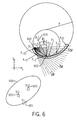
- FIG. 6 illustrates an example of High Resolution Compact Curved Grating with constant angle (the Constant-Angle Case);
- FIG. 7 shows a High Resolution Compact Curved Grating with Constant Arc (the Constant-Arc Case), the detector or output slit (or waveguide) SL 2 and the input slit (or waveguide) SL 1 being present on a tangent circle, in accordance with an embodiment of the present invention
- FIGS. 8A and 8B show a comparison between the Rowland design and the High Resolution Compact Curved Grating with constant groove (arc) length in accordance with the present invention.
- FIG. 9 illustrates a block diagram of a wavelength demultiplexer and a wavelength multiplexer.
- FIG. 10 illustrates a curved grating spectrometer configured as a wavelength multiplexer.
- FIG. 11 illustrates a curved grating spectrometer configured as a wavelength multiplexer.
- FIG. 12 illustrates a curved grating spectrometer configured as a wavelength multiplexer/demultiplexer.
- FIG. 13 illustrates a wavelength spectrometer configured as a multiplexer/demultiplexer with waveguides.
- FIG. 14 illustrates a high resolution compact curved grating.
- FIG. 15 illustrates a curved grating spectrometer configured as a wavelength multiplexer/demultiplexer.
- FIG. 16 illustrates a curved grating spectrometer configured as a wavelength multiplexer/demultiplexer.
- the present invention discloses a system comprising a compact curved grating (CCG), it associated compact curved grating spectrometer (CCGS) or wavelength Mux/deMux (WMDM) module and a method for making the same.
- the system is capable of achieving very small (resolution vs. size) RS factor.
- CCGS or WMDM module include an isolated optical spectrometer or wavelength Mux/deMux using discrete optical components such as slits, grating, spectrometer or wavelength Mux/deMux casing, detector, detector array, and motor drive. More generally, the CCGS or WMDM module could also be used as a wavelength dispersion element in a photonic integrated circuit.
- the photonic integrated circuit can be based on various materials including but not limited to glass (silica) waveguide, semiconductor waveguide, polymer nwaveguide, or any other type of optical waveguiding devices.
- Semiconductor waveguides include silicon or compound semiconductor waveguides such as III-V (GaAs, InP etc).
- the wavelength dispersion element based on the CCGS or WMDM module in the photonic integrated circuit can be integrated with optical detector, laser, amplifier, waveguide, modulator, splitter, multimode interference devices, other wavelength filters, array-waveguide-based devices, and other photonic devices, materials, or components to achieve a multi-component photonic integrated circuit with useful functionalities.
- the CCG explained below is a High-Resolution Compact Curved Grating (HR-CCG) that tries to alleviate the disadvantages associated with prior art mentioned earlier, by providing a high resolution in a small (compact) module.
- HR-CCG High-Resolution Compact Curved Grating
- a wavelength demultiplexer (wavelength deMux) 100 is a device in which multiple wavelengths in a beam of light 112 are separated into several different beams of light 114 .
- a wavelength multiplexer (wavelength Mux) 110 is a device in which multiple wavelengths in several beams of light 114 are combined to a single beam of light 112 .
- a curved grating spectrometer functions as a wavelength deMux 100 if it has an input slit 116 at the input beam 112 location so that the multiple wavelengths in the input beam will be diffracted to several output points 114 and several output slits 118 are placed at the locations of the spectrometer detectors mentioned above at these output points to form several output beams each with a different wavelength.
- the output slits 118 replace the detectors so that no detectors will be used.
- a curved grating spectrometer functions as a wavelength Mux 110 if it has multiple input slits 116 , each slit placed at an input beam's 114 location so that all the input beams 114 will be diffracted to the same output point and an output slit 118 is placed at the location of the spectrometer detector mentioned above so that the output slit 118 will give a single output beam of light 112 with the combined wavelengths of light.
- the output slit 118 replaced the detector so that no detector will then be used.
- a more general wavelength Mux/deMux device 120 will have multiple input slits 116 and multiple output slits so that several input beams of light 122 , each input beam with one or more wavelengths, are dispersed to form several output beams of light 124 , each output beam with one or several wavelengths.
- an integrated version of the wavelength Mux/deMux device 130 will use optical channel waveguides 132 replacing input and output slits in which the mouth of each channel waveguide 132 will be at the location of the slit it is replacing.
- the waveguides 132 can be formed by optical fibers or with multiple-layer dielectric materials with high-refractive-index core to guide optical waves in the form of channel or planar waveguides 132 .
- Such channel or planar waveguides can be formed on a common substrate.
- the input channel waveguide is connected to a planar waveguiding region that propagates the beam from the input waveguide mouth towards a grating etched vertically into the planar waveguide material.
- the back side of the grating (the side away from the planar waveguiding region) can be coated with metallic gold reflector.
- the beam diffracted from the grating is then coupled into an outout channel waveguide.
- the mouth of the output waveguide then acts as the exit slit or output slit.
- the width of the input waveguide mouth then defines the width of the input slit and the width of the output waveguide mouth defines the width of the output slit.
- the location of the input waveguide mouth defines the location of the input slit and the location of the output waveguide mouth defines the location of the output slit.
- the location of entrance slit or input slit (or waveguide) 502 can be adjusted in order to have the best performance for a particular design goal.
- the location of an input slit (or waveguide) 502 specified by angle ⁇ 1 with respect to the normal of grating center 504 and the distance S 1 from grating center 504 is not necessarily on a circle as in the case for Rowland design mentioned in the prior art.
- the normal of grating center 504 is a line segment (line EF in FIG. 5B ) that is perpendicular to the tangent to the grating-center curve (line AB in FIG. 5B ).
- the location of detector or output slit (or waveguide) can be adjusted in order to have the best performance for a particular design goal.
- the location of detector or output slit (or waveguide) 506 specified by the angle ⁇ 2 with respect to the normal of grating center 504 and the distance S 2 from the grating center is not necessarily on the same circle where entrance slit or input slit (or waveguide) 502 is located, nor on any other circle.
- n is the effective refractive index of propagation of the medium
- ⁇ c is the center of the operation wavelength
- three initial grooves are located on a circle radius R and have the initial groove spacing of d at the grating center. This circle segment of radius R at the grating center then forms the grating-center curve.
- the first of these conditions being that the path-difference between adjacent grooves should be an integral multiple of the wavelength in the medium.
- d 1 ( ⁇ 1 ,S 1 ,X i ) is the distance from a i-th groove located at X i to input slit (or input waveguide) 502 specified by ⁇ 1 and S 1
- d 2 ( ⁇ 2 ,S 2 ,X i ) is the distance from i-th groove located X i to detector or output slit (or waveguide) 502 specified by ⁇ 2 and S 2
- m is the diffraction order
- n is the effective refractive index of propagation of the medium.
- the second of these conditions being specific for a particular design goal of a curved-grating spectrometer.
- the unknown real variables in both equations Eq. (2) and Eq. (3) are x- and y-coordinates of the location vector X i of the i-th groove.
- the unknown real variables in both equations Eq. (2) and Eq. (3) are x- and y-coordinates of the location vector X i of the i-th groove.
- the last of the HR-CCG specification ensures that every ray from each groove focuses to a single point. This ensures HR-CCG having a large acceptance angle, and therefore a small spot size.
- FIG. 6 An exemplary embodiment of HR-CCG specified above is shown in FIG. 6 .
- entrance slit or input slit (or waveguide) SL 1 and detector or output slit (or waveguide) SL 2 are not located on a circle tangent to the grating-center.
- X in ( ⁇ S 1 *Sin( ⁇ 1 ), S 1 *Cos( ⁇ 1 )) is the position vector of entrance slit SL 1
- X det ( ⁇ S 2 *Sin( ⁇ 2 ), S 2 *Cos( ⁇ 2 )) is the position vector of detector or output slit (or waveguide) SL 2
- ⁇ i is the difference in angular position between successive i th and (i ⁇ 1) th grooves.
- operator “ ⁇ ” means the inner product in vector analysis and defined as A ⁇ B ⁇
- ” indicates taking the absolute value or the length of a vector. Because ⁇ i is constant for all grooves, it is same as the angular position difference between the center groove at X 0 and the first groove at X 1 , i.e.
- ⁇ 1 ArcCos ⁇ [ ( X 1 - X in ) ⁇ ( X 0 - X in )
- wave-front of the diverging input beam propagating toward the curved grating is sliced into a set of narrow beams with angular extension ⁇ by the curved-grating. Each beam with angular extension ⁇ undergoes reflective diffraction by each groove.
- diffraction at a particular groove is equivalent to redirecting to a particular narrow beam into a detector or output slit (or waveguide) SL 2 location with ⁇ 2 .
- the position vectors X i 's calculated from Eq. (2) and Eq. (4) are listed in the Table 2. As shown in FIG. 6 , the positions of grooves X i are not on a circle tangent to grating.
- the High-Resolution Compact Curved Grating has Constant Arc and the Detector or output slit (or waveguide) is located on a Circle tangent to the grating-center curve. This embodiment is described below in detail.
- both entrance slit or input slit (or waveguide) 502 and detector or output slit (or waveguide) 506 are located on a circle tangent to the grating-center curve as in the case of Rowland design mentioned earlier.
- grooves in this curved-grating are located such that the arc-length of each groove is the same (the Constant-Arc Case). As a result, grooves are not located on a circle nor are spaced with equal distance.
- the ideal shape of the groove at X i in a curved-grating is a section of ellipse 604 passing through X i with its two focal points (C 1 602 , C 2 603 ) at the input and output slits (SL 1 , SL 2 ). That is, if the focal point C 1 is at SL 1 and C 2 is at SL 2 for ellipse 604 passing though groove at X i , then the curved line segment G i 601 of the ellipse at X i will be the idea shape for the grove at X i .
- elliptic shape is used for each groove and the length of this elliptic shape in each groove is kept constant (constant arc). Center positions of the grooves X i 's in this example are determined so that the length of each elliptic groove is the same.
- the geometric specification of the HR-CCG with constant arc-length (the Constant-Arc Case) and detector or output slit (or waveguide) 506 at a circle tangent to the grating-center curve is as described below.
- the location of detector or output slit (or waveguide) can be adjusted in order to have the best performance for a particular design goal.
- the location of detector or output slit (or waveguide) 506 specified by the angle ⁇ 2 with respect to the normal of grating center 504 and the distance S 2 from the grating center is not necessarily on the same circle where entrance slit or input slit (or waveguide) 502 is located, nor on any other circle.
- the location of other grooves X i 's are obtained by the following two conditions.
- the second condition being the arc lengths of all the grooves are the same throughout the HR-CCG.
- This second condition can be mathematically expressed as
- FIG. 7 shows a specific example of the HR-CCG with constant arc-length of the grooves and detector or output slit (or waveguide) SL 2 at a tangent circle.
- Both entrance slit or input slit (or waveguide) SL 1 and exit slit or output slit (and waveguide) SL 12 are located on a tangent circle of radius 50 ⁇ m.
- the performance of the HR-CCG with the constant arc-length and detector or output slit (or waveguide) on a tangent circle is compared with a Rowland design with the same parameters such as ⁇ 1 , S 1 , ⁇ 2 , S 2 , R, m, d, and ⁇ c . It is a direct comparison of a Rowland curved-grating spectrometer described in FIG. 3 and a HRC-curved grating spectrometer described in FIG. 7 . All the configuration parameters are the same for these two spectrometers except the grating itself.
- Imaging properties that is, how well entrance slit or input slit (or waveguide) SL 1 is sharply imaged at the detector or output slit (or waveguide) location without aberration are compared.
- Imaging properties ultimately determine the resolution of a spectrometer.
- Finite Difference Time Domain (FDTD) method is used as a calculation method.
- FDTD is a Maxwell-equation solver, which evaluates electromagnetic wave within a spatial region for a certain period of time. By choosing a fine spatial grid size and temporal calculation step, the equation for an electromagnetic wave and its propagation can be solved with arbitrarily fine resolution.
- Imaging properties in these two curved-grating spectrometers is calculated by propagating a monochromatic light into entrance slit or input slit (or waveguide) 502 of each spectrometer.
- FDTD is run until the interference of beams from the entire grating groove is completed and forms an image of entrance slit or input slit (or waveguide) 502 at the detector or output slit (or waveguide) location.
- the resulting snapshot of electric-field near the detector or output slit (or waveguide) is taken for these two cases as shown in FIG. 8 .
- FIG. 8A shows the snapshot of electric field at the detector or output slit (or waveguide) location for the Rowland design described in FIG. 3 .
- the image of the entrance slit or input slit (or input waveguide mouth) is blurred due to imperfect grating.
- FIG. 8B shows the snapshot of electric field for the HR-CCG with constant arc-length grooves and detector or output slit (or waveguide) on a tangent circle.
- a sharp aberration free image of entrance slit or input slit (or input waveguide mouth) is formed at the detector or output slit (or waveguide) location.
- High-Resolution Compact Curved Grating has a constant arc with the detector or output slit (or waveguide) being present in-line. With reference to FIG. 7 , this embodiment can be realized if the input slit (or input waveguide) and exit slits (or outout slits or waveguides) are located along a line such that S 1 ⁇ S 2 . In another alternate embodiment, High-Resolution Compact Curved Grating has a constant arc with detector or output slit (or waveguide) SL 2 present at an arbitrary location.
- High-Resolution Compact Curved Grating has a constant angle and detector or output slit (or waveguide) SL 2 present on the circle of radius R 12 , as depicted in FIG. 6 .
- each groove surface has an angular extension ( ⁇ ) i from entrance slit or input slit (or waveguide) SL 1 .
- the angular extensions ( ⁇ ) i are kept constant for all grooves.
- both entrance slit or input slit (or waveguide) SL 1 and detectors or output slits or waveguides) SL 2 are located on or near a circle of radius R/2, where R is the radius of a circle formed by three initial groove locations X 0 , X 1 , and X 2 .
- High-Resolution Compact Curved Grating has a constant angle with detector or output slit (or waveguide) SL 2 present at an arbitrary location.
- High-Resolution Compact Curved Grating has groves lying on or near the circle of radius R (the near-Rowland Case) where R is the radius of a circle formed by three initial groove locations X 0 , X 1 , and X 2 , and the detector or output slit (or waveguide) SL 2 is present on the circle of radius R/2, as depicted in FIG. 14 .
- each groove surface has an angular extension ( ⁇ ) i from entrance slit or input slit (or waveguide).
- the angular extensions ( ⁇ ) i are chosen so that each groove lies on or near the circle of radius R.
- the location of other grooves X i 's are obtained by the following two conditions.
- each groove is located at or near the circle of radius R throughout the HR-CCG, where R is the radius of a circle formed by three initial groove locations X 0 , X 1 , and X 2 .
- the High-Resolution Compact Curved Grating with groves on or near the circle of radius R has detector or output slit (or waveguide) present at an arbitrary location.
- FIG. 15 shows an additional embodiment of a HR-CCG and an associated spectrometer or wavelength Mux/deMux utilizing the HR-CCG, called the Broadband Two-Wavelength Case.
- the HR-CCG spectrometer or wavelength Mux/deMux having the geometric configuration as described below.
- the location of the entrance slit or input slit (or waveguide) 902 is adjustable in order to have the best performance for a particular design goal.
- the location of a entrance slit or input slit (or waveguide) 902 specified by angle ⁇ 1 with respect to the normal of grating center 904 and the distance S 1 from grating center 904 is not necessarily on a circle as in the case for Rowland design mentioned in the prior art.
- the location of the detector or output slit (or waveguide) for two different wavelengths ⁇ 1 and ⁇ 2 is adjustable in order to have the best performance for a particular design goal.
- the location of the detector or output slit (or waveguide) 906 for wavelength ⁇ 1 is specified by the angle ⁇ 2 with respect to the normal of grating center 904 and the distance S 2 from the grating center.
- the location of detector or output slit (or waveguide) 908 for wavelength ⁇ 2 is specified by the angle ⁇ 3 with respect to the normal of grating center 904 and the distance S 3 from the grating center. Note that 906 , and 908 are not necessarily on the same circle where entrance slit or input slit (or waveguide) 902 is located, nor on any other circle.
- locations of other grooves X i 's are obtained by two conditions.
- the first of these conditions being that the path-difference between adjacent grooves should be an integral multiple of the wavelength ⁇ 1 in the medium.
- the second of these conditions being that the path-difference between adjacent grooves should be an integral multiple of the wavelength ⁇ 2 in the medium.
- d 3 ( ⁇ 3 ,S 3 ,X i ) is the distance from the i-th groove located at X i to detector or output slit (or waveguide) 908 specified by ⁇ 3 and S 3 .
- This mathematical expression is numerically exact for the optical path difference requirement in the diffraction grating and is actively adjusted for every groove on HR-CCG. Solving Equations (12) and (13) together, exact locations of other grooves X i 's can be obtained.
- FIG. 16 shows an additional embodiment of a HR-CCG and an associated spectrometer or wavelength Mux/deMux utilizing the HR-CCG.
- the distance S 2 from the grating center to the location of detector or output slit (or waveguide) 906 for wavelength ⁇ 1 is equal to the distance S 3 from the grating center to the location of detector or output slit (or waveguide) 908 for wavelength ⁇ 2 .
- ⁇ 1 As light at wavelength ⁇ 1 enters entrance slit or input slit (or waveguide) 902 and is diffracted by the grating towards 906 , it will hit the mirror and be reflected back by the mirror along the same path back to the grating and further focusing back to the entrance slit or input slit (or waveguide) 902 .
- the grating so generated gives rise to a third focal spot for a third input wavelength ⁇ 3 that has a value between wavelength ⁇ 1 and wavelength ⁇ 2 .
- the location of this third focal spot is 910 and is specified by angle ⁇ 4 with respect to the normal of grating center 904 and the distance S 4 from grating center 904 .
- the three output slit (or waveguide) locations 906 , 910 , 908 can be made to be located on a circle of radius R out , called the radius of curvature of the output plane or output-plane radius.
- S 2 and S 3 are chosen so that the locations 906 , 910 , 908 lie on a near straight line so that R out is large. This will ensure that the three focal points will form a nearly flat surface of reflection so that the focused beams with plane wavefront at their focal points will be reflected directly back to the entrance slit 902 . Each of the reflected beam will trace back its own original physical beam propagation and hence will achieve maximum reflection back into the input slit or waveguide 902
- the mirror locations are displaced at distance D away from locations 906 , 910 , and 908 so that the new locations 907 , 911 , and 909 lie on a new curved line 907 - 911 - 909 also with radius of curvature R out .
- a curve mirror reflecting surface is then placed or fabricated at curved line 907 - 911 - 909 .
- the beam at ⁇ 1 will hit the curved mirror at 907
- beam at ⁇ 3 will hit the curved mirror at 911
- beam at ⁇ 2 will hit the curved mirror at 909 .
Abstract
Description
d*(Sin(θ2)−Sin(θ1))=m*λ c /n (0)
| TABLE 1 | |||
| X−13 | (−54.6, 16.221) | ||
| X−12 | (−50.4, 13.630) | ||
| X−11 | (−46.2, 11.312) | ||
| X−10 | (−42, 9.248) | ||
| X−9 | (−37.8, 7.419) | ||
| X−8 | (−33.6, 5.814) | ||
| X−7 | (−29.4, 4.419) | ||
| X−6 | (−25.2, 3.227) | ||
| X−5 | (−21, 2.230) | ||
| X−4 | (−16.8, 1.421) | ||
| X−3 | (−12.6, 0.797) | ||
| X−2 | (−8.4, 0.353) | ||
| X−1 | (−4.2, 0.088) | ||
| X0 | (0, 0) | ||
| X1 | (4.2, 0.088) | ||
| X2 | (8.4, 0.353) | ||
| X3 | (12.6, 0.797) | ||
| X4 | (16.8, 1.421) | ||
| X5 | (21, 2.230) | ||
| X6 | (25.2, 3.227) | ||
d*(Sin(θ2)−Sin(θ1))=m*λ c /n (1)
[d 1(θ1 ,S 1 ,X i)+d 2(θ2 ,S 2 ,X i)]−[d 1(θ1 ,S 1 ,X i−1)+d 2(θ2 ,S 2 ,X i−1)]=m*λ/n, (2)
f(θ1 ,S 1,θ2 ,X i ,X i−1,λc n,m)=constant (3)
| X−10 | (−23.17, 15.28) | ||
| X−9 | (−22.24, 12.89) | ||
| X−8 | (−20.97, 10.60) | ||
| X−7 | (−19.36, 8.43) | ||
| X−6 | (−17.42, 6.44) | ||
| X−5 | (−15.17, 4.65) | ||
| X−4 | (−12.62, 3.10) | ||
| X−3 | (−9.80, 1.83) | ||
| X−2 | (−6.74, 0.87) | ||
| X−1 | (−3.60, 0.14) | ||
| X0 | (0.00, 0.00) | ||
| X1 | (3.60, 0.14) | ||
| X2 | (7.30, 0.70) | ||
| X3 | (11.06, 1.70) | ||
| X4 | (14.83, 3.13) | ||
| X5 | (18.57, 5.02) | ||
| X6 | (22.22, 7.36) | ||
| X7 | (25.73, 10.16) | ||
| X8 | (29.06, 13.39) | ||
| X9 | (32.16, 17.06) | ||
| X10 | (34.98, 21.15) | ||
[d 1(θ1 ,S 1 ,X i)+d 2(θ2 ,S 2 ,X i)]−[d 1(θ1 ,S 1 ,X i−1)+d 2(θ2 ,S 2 ,X i−1)]=m*λ/n, (6)
| X−15 | (−55.43, 23.48) | ||
| X−14 | (−52.90, 20.32) | ||
| X−13 | (−50.07, 17.38) | ||
| X−12 | (−46.98, 14.68) | ||
| X−11 | (−43.67, 12.21) | ||
| X−10 | (−40.17, 9.98) | ||
| X−9 | (−36.52, 7.99) | ||
| X−8 | (−32.74, 6.24) | ||
| X−7 | (−28.84, 4.72) | ||
| X−6 | (−24.86, 3.43) | ||
| X−5 | (−20.81, 2.35) | ||
| X−6 | (−16.71, 1.48) | ||
| X−5 | (−20.81, 2.35) | ||
| X−4 | (−16.71, 1.48) | ||
| X−3 | (−12.57, 0.82) | ||
| X−2 | (−8.39, 0.36) | ||
| X−1 | (−4.20, 0.09) | ||
| X0 | (0.00, 0.00) | ||
| X1 | (4.20, 0.09) | ||
| X2 | (8.39, 0.35) | ||
| X3 | (12.57, 0.77) | ||
| X4 | (16.73, 1.34) | ||
| X5 | (20.86, 2.07) | ||
| X6 | (24.97, 2.94) | ||
| X7 | (29.04, 3.96) | ||
| X8 | (33.07, 5.10) | ||
| X9 | (37.06, 6.37) | ||
| X10 | (41.01, 7.76) | ||
| X11 | (44.91, 9.28) | ||
| X12 | (48.77, 10.90) | ||
| X13 | (52.57, 12.63) | ||
| X14 | (56.33, 14.47) | ||
[d 1(θ1 ,S 1 ,X i)+d 2(θ2 ,S 2 ,X i)]−[d 1(θ1 ,S 1 ,X i−1)+d 2(θ2 ,S 2 ,X i−1)]=m*λ/n (9)
d*(Sin(θ2)−Sin(θ1))=m*λ 1 /n (10)
d*(Sin(θ3)−Sin(θ1))=m*λ 2 /n (11)
where m is the diffraction order and n is the effective refractive index of propagation of the medium.
[d 1(θ1 ,S 1 ,X i)+d 2(θ2 ,S 2 ,X i)]−[d 1(θ1 ,S 1 ,X i−1)+d 2(θ2 ,S 2 ,X i−1)]=m*λ 1 /n, (12)
where d1(θ1,S1,Xi) is the distance from the i-th groove located at Xi to entrance slit or input slit (or waveguide) 902 specified by θ1 and S1, d2(θ2,S2,Xi) is the distance from the i-th groove located at Xi to detector or output slit (or waveguide) 906 specified by θ2 and S2, m is the diffraction order, and n is the effective refractive index of propagation of the medium. This mathematical expression is numerically exact for the optical path difference requirement in the diffraction grating and is actively adjusted for every groove on HR-CCG.
[d 1(θ1 ,S 1 ,X i)+d 3(θ3 ,S 3 ,X i)]−[d 1(θ1 ,S 1 ,X i−1)+d 3(θ3 ,S 3 ,X i−1)]=m*λ 2 /n, (13)
Claims (7)
Priority Applications (2)
| Application Number | Priority Date | Filing Date | Title |
|---|---|---|---|
| US13/911,847 US8854620B2 (en) | 2004-03-20 | 2013-06-06 | Curved grating spectrometer and wavelength multiplexer or demultiplexer with very high wavelength resolution |
| US14/482,615 US9612155B2 (en) | 2004-03-20 | 2014-09-10 | Curved grating spectrometer and wavelength multiplexer or demultiplexer with very high wavelength resolution |
Applications Claiming Priority (4)
| Application Number | Priority Date | Filing Date | Title |
|---|---|---|---|
| US10/708,730 US7283233B1 (en) | 2004-03-20 | 2004-03-20 | Curved grating spectrometer with very high wavelength resolution |
| US11/872,455 US7623235B2 (en) | 2004-03-20 | 2007-10-15 | Curved grating spectrometer with very high wavelength resolution |
| US12/623,750 US8462338B1 (en) | 2004-03-20 | 2009-11-23 | Curved grating spectrometer and wavelength multiplexer or demultiplexer with very high wavelength resolution |
| US13/911,847 US8854620B2 (en) | 2004-03-20 | 2013-06-06 | Curved grating spectrometer and wavelength multiplexer or demultiplexer with very high wavelength resolution |
Related Parent Applications (1)
| Application Number | Title | Priority Date | Filing Date |
|---|---|---|---|
| US12/623,750 Division US8462338B1 (en) | 2004-03-20 | 2009-11-23 | Curved grating spectrometer and wavelength multiplexer or demultiplexer with very high wavelength resolution |
Related Child Applications (1)
| Application Number | Title | Priority Date | Filing Date |
|---|---|---|---|
| US14/482,615 Continuation-In-Part US9612155B2 (en) | 2004-03-20 | 2014-09-10 | Curved grating spectrometer and wavelength multiplexer or demultiplexer with very high wavelength resolution |
Publications (2)
| Publication Number | Publication Date |
|---|---|
| US20130272695A1 US20130272695A1 (en) | 2013-10-17 |
| US8854620B2 true US8854620B2 (en) | 2014-10-07 |
Family
ID=48538404
Family Applications (2)
| Application Number | Title | Priority Date | Filing Date |
|---|---|---|---|
| US12/623,750 Active - Reinstated 2025-10-21 US8462338B1 (en) | 2004-03-20 | 2009-11-23 | Curved grating spectrometer and wavelength multiplexer or demultiplexer with very high wavelength resolution |
| US13/911,847 Expired - Lifetime US8854620B2 (en) | 2004-03-20 | 2013-06-06 | Curved grating spectrometer and wavelength multiplexer or demultiplexer with very high wavelength resolution |
Family Applications Before (1)
| Application Number | Title | Priority Date | Filing Date |
|---|---|---|---|
| US12/623,750 Active - Reinstated 2025-10-21 US8462338B1 (en) | 2004-03-20 | 2009-11-23 | Curved grating spectrometer and wavelength multiplexer or demultiplexer with very high wavelength resolution |
Country Status (1)
| Country | Link |
|---|---|
| US (2) | US8462338B1 (en) |
Cited By (2)
| Publication number | Priority date | Publication date | Assignee | Title |
|---|---|---|---|---|
| US10151631B2 (en) | 2016-10-04 | 2018-12-11 | Kla-Tencor Corporation | Spectroscopy with tailored spectral sampling |
| TWI690727B (en) * | 2018-02-09 | 2020-04-11 | 鴻海精密工業股份有限公司 | Freeform surface imaging spectrometer system |
Families Citing this family (7)
| Publication number | Priority date | Publication date | Assignee | Title |
|---|---|---|---|---|
| US9612155B2 (en) * | 2004-03-20 | 2017-04-04 | Electronic Photonic Ic Inc. (Epic Inc.) | Curved grating spectrometer and wavelength multiplexer or demultiplexer with very high wavelength resolution |
| US8213751B1 (en) | 2008-11-26 | 2012-07-03 | Optonet Inc. | Electronic-integration compatible photonic integrated circuit and method for fabricating electronic-integration compatible photonic integrated circuit |
| CN105593747B (en) * | 2013-06-09 | 2019-07-05 | 光电网股份有限公司 | The wide modulation bandwidth low optical losses optical strength of ultra low voltage or phase-modulator |
| US10353224B2 (en) * | 2013-06-09 | 2019-07-16 | Electronic Photonic Ic Inc. (Epic Inc.) | Optical signal processing devices with high device performances |
| CN109682469B (en) * | 2014-09-10 | 2021-04-02 | 电子光子集成电路股份有限公司 | Curved grating spectrometer and wavelength multiplexer or demultiplexer with extremely high wavelength resolution |
| CN111025464A (en) * | 2019-12-17 | 2020-04-17 | 湖北工业大学 | Etched diffraction grating type wavelength division multiplexer/demultiplexer based on SU8 glue |
| CN112859246B (en) * | 2020-12-31 | 2023-08-18 | 武汉科宇智联信息技术有限公司 | Echelle grating flat-top type demultiplexer |
Citations (11)
| Publication number | Priority date | Publication date | Assignee | Title |
|---|---|---|---|---|
| US4027975A (en) * | 1974-05-28 | 1977-06-07 | National Research Development Corporation | Scanning monochromator and concave reflecting grating employed therein |
| US4140394A (en) | 1977-06-06 | 1979-02-20 | Baird Corporation | Spectrometer sequential readout system |
| US4380393A (en) | 1980-03-31 | 1983-04-19 | Nippon Kogaku K.K. | Grazing incidence spectrometer |
| US4571074A (en) * | 1982-01-04 | 1986-02-18 | Instruments S.A. | Spectrometry device for analyzing polychromatic light |
| US4820046A (en) | 1986-12-01 | 1989-04-11 | Hitachi, Ltd. | Spectroscope apparatus and reaction apparatus using the same |
| US5066127A (en) * | 1989-08-29 | 1991-11-19 | Hyperfine, Inc. | Stigmatic imaging with spherical concave diffraction gratings |
| US5114231A (en) | 1989-09-05 | 1992-05-19 | Instrument Sa | Spectroscopic analysis device |
| US6339662B1 (en) | 1998-07-30 | 2002-01-15 | National Research Council Of Canada | Wavelength stabilized planar waveguide optical devices incorporating a dispersive element |
| US20040196458A1 (en) * | 2003-04-02 | 2004-10-07 | Olympus Corporation | Spectrophotometer |
| US6878562B2 (en) | 2000-10-20 | 2005-04-12 | Phosistor Technologies, Incorporated | Method for shifting the bandgap energy of a quantum well layer |
| US7283233B1 (en) | 2004-03-20 | 2007-10-16 | Seng-Tiong Ho | Curved grating spectrometer with very high wavelength resolution |
-
2009
- 2009-11-23 US US12/623,750 patent/US8462338B1/en active Active - Reinstated
-
2013
- 2013-06-06 US US13/911,847 patent/US8854620B2/en not_active Expired - Lifetime
Patent Citations (11)
| Publication number | Priority date | Publication date | Assignee | Title |
|---|---|---|---|---|
| US4027975A (en) * | 1974-05-28 | 1977-06-07 | National Research Development Corporation | Scanning monochromator and concave reflecting grating employed therein |
| US4140394A (en) | 1977-06-06 | 1979-02-20 | Baird Corporation | Spectrometer sequential readout system |
| US4380393A (en) | 1980-03-31 | 1983-04-19 | Nippon Kogaku K.K. | Grazing incidence spectrometer |
| US4571074A (en) * | 1982-01-04 | 1986-02-18 | Instruments S.A. | Spectrometry device for analyzing polychromatic light |
| US4820046A (en) | 1986-12-01 | 1989-04-11 | Hitachi, Ltd. | Spectroscope apparatus and reaction apparatus using the same |
| US5066127A (en) * | 1989-08-29 | 1991-11-19 | Hyperfine, Inc. | Stigmatic imaging with spherical concave diffraction gratings |
| US5114231A (en) | 1989-09-05 | 1992-05-19 | Instrument Sa | Spectroscopic analysis device |
| US6339662B1 (en) | 1998-07-30 | 2002-01-15 | National Research Council Of Canada | Wavelength stabilized planar waveguide optical devices incorporating a dispersive element |
| US6878562B2 (en) | 2000-10-20 | 2005-04-12 | Phosistor Technologies, Incorporated | Method for shifting the bandgap energy of a quantum well layer |
| US20040196458A1 (en) * | 2003-04-02 | 2004-10-07 | Olympus Corporation | Spectrophotometer |
| US7283233B1 (en) | 2004-03-20 | 2007-10-16 | Seng-Tiong Ho | Curved grating spectrometer with very high wavelength resolution |
Cited By (2)
| Publication number | Priority date | Publication date | Assignee | Title |
|---|---|---|---|---|
| US10151631B2 (en) | 2016-10-04 | 2018-12-11 | Kla-Tencor Corporation | Spectroscopy with tailored spectral sampling |
| TWI690727B (en) * | 2018-02-09 | 2020-04-11 | 鴻海精密工業股份有限公司 | Freeform surface imaging spectrometer system |
Also Published As
| Publication number | Publication date |
|---|---|
| US20130272695A1 (en) | 2013-10-17 |
| US8462338B1 (en) | 2013-06-11 |
Similar Documents
| Publication | Publication Date | Title |
|---|---|---|
| US7623235B2 (en) | Curved grating spectrometer with very high wavelength resolution | |
| US8854620B2 (en) | Curved grating spectrometer and wavelength multiplexer or demultiplexer with very high wavelength resolution | |
| US9939320B2 (en) | Curved grating spectrometer and wavelength multiplexer or demultiplexer with very high wavelength resolution | |
| US9176282B2 (en) | High efficiency mono-order concave diffraction grating | |
| US7889336B2 (en) | Optical integrated nanospectrometer | |
| US7283233B1 (en) | Curved grating spectrometer with very high wavelength resolution | |
| CA2518691C (en) | Wavelength dispersive fourier transform spectrometer | |
| US9310564B2 (en) | Multiport tunable optical filters | |
| US7295330B2 (en) | Film mapping system | |
| US9472922B2 (en) | Wavelength-tunable light source | |
| Bland-Hawthorn et al. | Instruments without optics: an integrated photonic spectrograph | |
| Lycett et al. | Perfect chirped echelle grating wavelength multiplexor: design and optimization | |
| US9574941B2 (en) | Dispersed fourier transform spectrometer, methods and systems | |
| US9612155B2 (en) | Curved grating spectrometer and wavelength multiplexer or demultiplexer with very high wavelength resolution | |
| JPH04234704A (en) | Diffraction grating with plurality of output end face, on which optical guide is arranged in parallel | |
| US10866360B2 (en) | Broadband multifunctional efficient meta-gratings based on dielectric waveguide phase shifters | |
| EP1509980B1 (en) | Resonator | |
| Wu et al. | Design considerations for Rowland circle gratings used in photonic integrated devices for WDM applications | |
| JP2009121986A (en) | Spectral apparatus | |
| WO2010140998A1 (en) | Optical integrated nanospectrometer and method of manufacturing thereof | |
| US7212560B2 (en) | Tunable external cavity laser diode using variable optical deflector | |
| Chen et al. | Planar concave grating demultiplexer for coarse WDM based on confocal ellipses | |
| Pottier et al. | Design and properties of concave diffraction gratings based on elliptical Bragg mirrors | |
| Zektzer et al. | Interferometric method for phase error measurement in an arrayed waveguide grating with a free space output | |
| Grabarnik et al. | IC-compatible microspectrometer using a planar imaging diffraction grating |
Legal Events
| Date | Code | Title | Description |
|---|---|---|---|
| FEPP | Fee payment procedure |
Free format text: MAINTENANCE FEE REMINDER MAILED (ORIGINAL EVENT CODE: REM.) |
|
| LAPS | Lapse for failure to pay maintenance fees |
Free format text: PATENT EXPIRED FOR FAILURE TO PAY MAINTENANCE FEES (ORIGINAL EVENT CODE: EXP.); ENTITY STATUS OF PATENT OWNER: SMALL ENTITY |
|
| STCH | Information on status: patent discontinuation |
Free format text: PATENT EXPIRED DUE TO NONPAYMENT OF MAINTENANCE FEES UNDER 37 CFR 1.362 |
|
| FP | Lapsed due to failure to pay maintenance fee |
Effective date: 20181007 |
|
| FEPP | Fee payment procedure |
Free format text: PETITION RELATED TO MAINTENANCE FEES FILED (ORIGINAL EVENT CODE: PMFP); ENTITY STATUS OF PATENT OWNER: SMALL ENTITY Free format text: PETITION RELATED TO MAINTENANCE FEES GRANTED (ORIGINAL EVENT CODE: PMFG); ENTITY STATUS OF PATENT OWNER: SMALL ENTITY Free format text: SURCHARGE, PETITION TO ACCEPT PYMT AFTER EXP, UNINTENTIONAL. (ORIGINAL EVENT CODE: M2558); ENTITY STATUS OF PATENT OWNER: SMALL ENTITY |
|
| MAFP | Maintenance fee payment |
Free format text: PAYMENT OF MAINTENANCE FEE, 4TH YR, SMALL ENTITY (ORIGINAL EVENT CODE: M2551); ENTITY STATUS OF PATENT OWNER: SMALL ENTITY Year of fee payment: 4 |
|
| STCF | Information on status: patent grant |
Free format text: PATENTED CASE |
|
| AS | Assignment |
Owner name: HUANG, YINGYAN, ILLINOIS Free format text: ASSIGNMENT OF ASSIGNORS INTEREST;ASSIGNOR:OPTONET INC.;REEL/FRAME:057010/0080 Effective date: 20210621 |
|
| AS | Assignment |
Owner name: HUANG, YINGYAN, ILLINOIS Free format text: ASSIGNMENT OF ASSIGNORS INTEREST;ASSIGNOR:HO, SENG-TIONG;REEL/FRAME:057506/0259 Effective date: 20210915 |
|
| MAFP | Maintenance fee payment |
Free format text: PAYMENT OF MAINTENANCE FEE, 8TH YR, SMALL ENTITY (ORIGINAL EVENT CODE: M2552); ENTITY STATUS OF PATENT OWNER: SMALL ENTITY Year of fee payment: 8 |