US8856417B2 - Memory module connector with auxiliary power cable - Google Patents
Memory module connector with auxiliary power cable Download PDFInfo
- Publication number
- US8856417B2 US8856417B2 US13/647,770 US201213647770A US8856417B2 US 8856417 B2 US8856417 B2 US 8856417B2 US 201213647770 A US201213647770 A US 201213647770A US 8856417 B2 US8856417 B2 US 8856417B2
- Authority
- US
- United States
- Prior art keywords
- memory module
- memory
- power cable
- auxiliary power
- auxiliary
- Prior art date
- Legal status (The legal status is an assumption and is not a legal conclusion. Google has not performed a legal analysis and makes no representation as to the accuracy of the status listed.)
- Active, expires
Links
Images

Classifications
-
- G—PHYSICS
- G06—COMPUTING; CALCULATING OR COUNTING
- G06F—ELECTRIC DIGITAL DATA PROCESSING
- G06F1/00—Details not covered by groups G06F3/00 - G06F13/00 and G06F21/00
- G06F1/26—Power supply means, e.g. regulation thereof
-
- G—PHYSICS
- G06—COMPUTING; CALCULATING OR COUNTING
- G06F—ELECTRIC DIGITAL DATA PROCESSING
- G06F1/00—Details not covered by groups G06F3/00 - G06F13/00 and G06F21/00
- G06F1/16—Constructional details or arrangements
- G06F1/18—Packaging or power distribution
- G06F1/183—Internal mounting support structures, e.g. for printed circuit boards, internal connecting means
- G06F1/185—Mounting of expansion boards
Definitions
- the present invention relates to memory module connectors, and more particularly to a memory module connector that provides auxiliary power to a memory module.
- Computer systems range from smaller, general purpose computers suitable for household and office use, to larger and more specialized computer systems.
- a personal computer is an example of a general-purpose computer that has a selection of hardware and peripherals suitable for an individual user.
- a desktop computer is a PC that is designed to be set up and used for an extended period of time at a fixed location having access to an electrical power outlet.
- a laptop computer has the same general capabilities of a desktop, along with features for enhanced mobility, such as lighter weight, an integrated display, and a battery pack for use at a variety of locations even where a building power outlet is unavailable.
- a server is another type of computer configured for serving the needs of multiple users simultaneously, which has particular utility in business environments.
- a larger system of interconnected servers may be consolidated in a single location for centralized system administration, and to provide access to multiple users over a network.
- Short-term memory provides a large storage capacity of a non-volatile (i.e. persistent) type, which persists even when the system is in a powered-off state.
- the most common long-term memory devices include hard disk drives (HDD) with rotating magnetic disks and newer solid-state devices (SSD) that require no moving parts for storage.
- HDD hard disk drives
- SSD newer solid-state devices
- Short-term memory referred to usually as “system memory,” typically has much less storage capacity but also much faster access times than long-term memory.
- Short-term memory devices typically comprise memory modules with dynamic random access memory (DRAM) chips.
- DRAM dynamic random access memory
- DRAM chips are a transient (volatile) SSD, in that the DRAM chips have no moving parts but require constant power and a refresh rate.
- the relatively large capacity and persistent storage of long-term memory devices are suitable for storing software applications, data, and files indefinitely until ready for use by the computer system.
- selected software instructions and data may then be retrieved from long-term memory into short-term memory for faster, more efficient execution by a processor directly from short-term memory.
- a disclosed apparatus includes a memory module, a memory module socket, and an auxiliary power cable for providing an increased voltage to the memory module.
- the memory module includes a semiconductor card having horizontal upper and lower card edges, a pair of vertical card edges, and a pair of opposing card faces. One or more persistent-storage memory chips are provided on one or both card faces.
- An auxiliary voltage connector is provided along at least one of the vertical card edges in electrical communication with the one or more memory chips.
- the memory module socket receives and supports the memory module at the lower card edge.
- the auxiliary power cable is coupled at one end to an electronic power source on the system board. A connector at the other end plugs in to the auxiliary voltage connector on the memory module to provide power from the electronic power source to the one or more memory chips.
- the auxiliary power cable resists movement of a latch lever when plugged in to the memory module. Removing the memory module from the socket requires disconnecting the auxiliary power cable from at least one end.
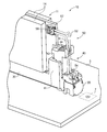
- FIG. 1 is a perspective view of a memory system with a persistent, solid-state memory module inserted into a complimentary memory module socket.
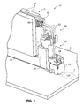
- FIG. 2 is a FIG. 2 is an enlarged view of one end of the memory system 10 of FIG. 1 .
- FIG. 3 is a further enlarged view of the memory system at the same end as in FIG. 2 , further detailing features of the latch, cable, and memory module.
- a memory module that incorporates a persistent (i.e. non-volatile) solid-state memory structure as an alternative to a conventional DIMM.
- the memory module may have a form factor comparable to that of a standard dual in-line memory module (DIMM) and can be used instead of a conventional DIMM as system memory.
- the persistent storage structure may include only non-volatile storage chips, such as NAND flash memory chips.
- the persistent storage structure may include a combination of volatile (e.g. DRAM) and non-volatile (NAND flash) memory chips.
- the NAND flash chips or other persistent-storage devices use a higher voltage (e.g. 3.3V) than provided by a conventional DIMM socket (e.g. 1.5V).
- An auxiliary power cable is used to connect an auxiliary voltage source on the system board to an auxiliary voltage connector on the memory module.
- the auxiliary voltage source is at a higher voltage (e.g. 12V), which can be transformed more efficiently down to 3.3V than a lower standard DIMM voltage (e.g. 1.5V) could be transformed up to 3.3V.
- a latch on the socket includes a receptacle for receiving the auxiliary power cable.
- the cable is routed along an outer portion of the lever to interfere with movement of the lever. Ejecting the memory module requires first disconnecting the auxiliary power cable from the memory module. This avoids inadvertently ejecting the memory module while powering the memory module, to protect the memory module from damage.
- FIG. 1 is a perspective view of a memory system 10 with a persistent, solid-state memory module 11 in a fully received position in a memory module socket 30 .
- the socket 30 is an electrical memory module connector mounted on a system board 5 that receives the memory module 11 in a downward insertion direction 23 .
- a latch 40 is provided at each end of the socket 30 for selectively securing the memory module 11 in a fully-seated position within socket 30 .
- the memory module 11 includes a semiconductor card 12 with a persistent storage structure 14 on the opposing faces 19 of the semiconductor card 12 .
- the semiconductor card 12 is a thin, substantially rectangular substrate, with opposing faces 19 bordered by opposing upper and lower card edges 15 , 16 and opposing vertical card edges 17 , 18 .
- the persistent storage structure 14 is a non-transient, solid-state device (SSD), which may comprise NAND flash memory, for example.
- SSD non-transient, solid-state device
- the persistent storage structure 14 is generically depicted as a unitary structure spanning each face 19 of semiconductor card 12 , but may comprise any number of memory devices or chips 14 C secured along the card face 19 as indicated using dashed lines.
- the memory module 11 may be a Flash DIMM wherein the persistent storage structure consists entirely of persistent (non-volatile) memory chips.
- the memory module 11 may be an NV-DIMM with a combination of both volatile and non-volatile memory chips. In an NV-DIMM, the memory stored in volatile memory chips when the computer is powered on gets backed up onto non-volatile memory chips in the event of a power loss.
- a schematically-shown processor (CPU) 70 and included memory controller 72 are in communication with the socket 30 over a memory bus 74 .
- the socket 30 provides an input/output (I/O) and power interface between the memory controller 72 and the memory module 11 .
- a plurality of socket contacts (not shown) within the socket are aligned with corresponding card edge contacts 22 on the lower card edge 16 for carrying electronic signals between the CPU 70 and the memory module 11 so that the CPU 70 can selectively store and retrieve data on the persistent storage structure 14 .
- the memory controller 72 may be capable of recognizing and interchangeably controlling either the disclosed memory module 11 or a conventional DIMM.
- FIG. 2 is an enlarged view of one end of the memory system 10 of FIG. 1 .
- the latch 40 includes a latch tower 41 and a lever 42 that is pivotably coupled to the latch tower 41 .
- a finger grip 44 on the lever 42 is shaped and textured for pivoting the lever 42 by hand, between an open (i.e. unlatched) position and a closed (i.e. latched) position (shown in FIG. 2 ).
- Moving the lever 42 inward to the latched position locks the memory module 11 within the socket 30 , and may also urge the memory module 11 toward the fully seated position. Alternately moving the lever outward to the unlatched position unlocks the memory module 11 and may also eject the memory module 11 .
- the socket 30 may be configured to interchangeably receive the memory module 11 or a conventional DIMM.
- the socket 30 provides a standard DIMM voltage (e.g. 1.5 V) for when a conventional DIMM is received by the socket 30 .
- the persistent storage structures 14 on the disclosed memory module 11 require a higher voltage, however, which is supplied using an auxiliary power cable 50 .
- the cable 50 in this embodiment comprises first and second (+ and ⁇ ) wires 51 , 52 externally routed from the system board 5 to the memory module 11 .
- a first connector pair 54 , 55 includes a connector 54 at a first end of the cable 50 that connects to a corresponding connector 55 on the system board 5 , to couple the cable 50 to a 12 V power source 7 on the system board 5 .
- a second connector pair 56 , 57 includes a connector 56 at a second end of the cable 50 that plugs into a corresponding auxiliary voltage connector 57 on the memory module 11 .
- the power source 7 may comprise printed circuit board voltage wires or a printed circuit board power plane.
- the cable 50 may remain connected at the first end to the power source 7 (by the first connector pair 54 , 55 ) whether the memory module 11 is present in the socket 30 or not.
- the second end of the cable 50 may be selectively connected or disconnected from the memory module 11 by the second connector pair 56 , 57 .
- Power at 12 V for example, is supplied to the memory module 11 by plugging the cable 50 in to the memory module 11 .
- the cable 50 is optionally positioned and routed to deliberately interfere with movement of the lever 42 when connected to the memory module 11 .
- the length of the cable 50 may also be made short enough to resist or prevent the latch from being fully moved to the unlatched position while the cable 50 is plugged in, despite the flexibility of the cable 50 . This intentional interference requires the cable 50 to be unplugged from the memory module 11 before ejecting the memory module 11 from the socket 30 .
- the wires 51 , 52 of the cable 50 may be sufficiently rigid to maintain the shape shown, yet sufficiently flexible (i.e. elastically deformable) so that the wires 51 , 52 return to their original shape if flexed and released.
- the flexibility of the wires 51 , 52 facilitates connecting and disconnecting the cable 50 from the memory module 11 .
- the use of separate wires 51 , 52 enclosed in separate wire housings may contribute to the flexibility of the cable 50 , as compared with having both wires 51 , 52 enclosed in a single housing.
- the cable 50 To eject the memory module 11 from the socket 30 , the cable 50 must first be disconnected at least from one end (typically, unplugged from the memory module 11 at the connector pair 56 , 57 ), so that the cable 50 can then be easily flexed enough to move the latch lever 42 to the unlatched position.
- the cable 50 may be disconnected at both ends (rather than leaving the cable 50 attached at one end) and removed entirely from the rest of the memory system 10 to facilitate subsequent removal of the memory module 11 .
- Each connector pair 54 , 55 and 56 , 57 could comprise connector types that are easily disconnected by hand without special tools.
- the practice of removing the cable 50 from both ends before operating the lever 42 requires little to no flexing of the cable 50 , allowing the cable 50 to be made more rigid. A more rigid cable can further resist movement of the lever 42 and minimize the likelihood of inadvertently ejecting the memory module 11 while the cable 50 is connected.
- FIG. 3 is a further enlarged view of the memory system 10 at the same end as in FIG. 2 , further detailing features of the latch 40 , cable 50 , and memory module 11 .
- the lever 42 includes a pair of adjacent receptacles 46 , 47 .
- the receptacles 46 , 47 in this embodiment comprise recesses in the lever 42 , which may be formed in the lever 42 by molding.
- Other suitable receptacles could be used, such as intermediary fasteners configured for securing the wires 51 , 52 to the lever 42 .
- Each receptacle 46 laterally receives a respective one of the wires 51 , 52 .
- Each wire 51 , 52 may have an interference fit with the respective receptacle 46 , 47 , so that the wires “snap into” and are thereby retained by the receptacles 46 , 47 .
- the pair of connectors 56 , 57 in this embodiment are z-axis connectors that connect in a z-axis direction labeled in the figure, which is perpendicular to a plane of the memory module 11 .
- the cable 50 may be flexed to connect and disconnect the connectors 56 , 57 while the wires 51 , 52 are received within the receptacles 46 , 47 . Because the cable 50 has two separate wires 51 , 52 in the example embodiment of FIG.
- separate receptacles are formed on the lever 42 for receiving the two wires 51 , 52 .
- the two wires may be enclosed within a single cable housing, so that just a single receptacle on the lever 42 is needed for receiving the single-housing auxiliary power cable.
Abstract
Description
Claims (14)
Priority Applications (1)
| Application Number | Priority Date | Filing Date | Title |
|---|---|---|---|
| US13/647,770 US8856417B2 (en) | 2012-10-09 | 2012-10-09 | Memory module connector with auxiliary power cable |
Applications Claiming Priority (1)
| Application Number | Priority Date | Filing Date | Title |
|---|---|---|---|
| US13/647,770 US8856417B2 (en) | 2012-10-09 | 2012-10-09 | Memory module connector with auxiliary power cable |
Publications (2)
| Publication Number | Publication Date |
|---|---|
| US20140098480A1 US20140098480A1 (en) | 2014-04-10 |
| US8856417B2 true US8856417B2 (en) | 2014-10-07 |
Family
ID=50432494
Family Applications (1)
| Application Number | Title | Priority Date | Filing Date |
|---|---|---|---|
| US13/647,770 Active 2032-12-26 US8856417B2 (en) | 2012-10-09 | 2012-10-09 | Memory module connector with auxiliary power cable |
Country Status (1)
| Country | Link |
|---|---|
| US (1) | US8856417B2 (en) |
Cited By (1)
| Publication number | Priority date | Publication date | Assignee | Title |
|---|---|---|---|---|
| US9600040B1 (en) * | 2015-10-13 | 2017-03-21 | Evga Corporation | Interface card adapting device and method thereof |
Families Citing this family (13)
| Publication number | Priority date | Publication date | Assignee | Title |
|---|---|---|---|---|
| US9740249B2 (en) * | 2014-01-30 | 2017-08-22 | Hewlett Packard Enterprise Development Lp | Mounting device |
| USD743399S1 (en) * | 2014-05-30 | 2015-11-17 | Emc Corporation | Flash module |
| CN105786099B (en) * | 2014-12-26 | 2019-03-15 | 鸿富锦精密工业(武汉)有限公司 | Adapter |
| WO2016133535A1 (en) | 2015-02-20 | 2016-08-25 | Hewlett Packard Enterprise Development Lp | Tool-less multipoint latching mechanism |
| KR20160131171A (en) * | 2015-05-06 | 2016-11-16 | 에스케이하이닉스 주식회사 | Memory module including battery |
| US11257527B2 (en) | 2015-05-06 | 2022-02-22 | SK Hynix Inc. | Memory module with battery and electronic system having the memory module |
| USD815641S1 (en) * | 2015-11-10 | 2018-04-17 | Sunland International, Llc | Removable SSD device |
| WO2017127065A1 (en) * | 2016-01-20 | 2017-07-27 | Hewlett Packard Enterprise Development Lp | Power-loss protection for plug-in module |
| USD857020S1 (en) * | 2016-05-25 | 2019-08-20 | Tdk Corporation | Piezoelectric element |
| JP1565481S (en) * | 2016-05-25 | 2016-12-19 | ||
| CN111045492B (en) * | 2019-12-09 | 2021-03-12 | 宁波市圣鑫达传动科技有限公司 | Multi-slot type memory bank fixing device based on lead screw transmission principle |
| WO2022047308A1 (en) * | 2020-08-28 | 2022-03-03 | Schlumberger Technology Corporation | Wireless switch for perforation tool |
| US11789877B2 (en) * | 2021-08-27 | 2023-10-17 | Dell Products, L.P. | Removable memory module coupling |
Citations (42)
| Publication number | Priority date | Publication date | Assignee | Title |
|---|---|---|---|---|
| US3673669A (en) | 1970-11-19 | 1972-07-04 | Sperry Rand Corp | Method of making side entry card guides |
| US4008942A (en) | 1975-07-29 | 1977-02-22 | General Signal Corporation | Printed circuit board holding spring |
| US4057879A (en) * | 1975-03-12 | 1977-11-15 | E. I. Du Pont De Nemours And Company | Headers with insertable latch members |
| US4818240A (en) | 1987-10-30 | 1989-04-04 | International Business Machines Corporation | Power rails for edge mounting modules |
| US4906197A (en) * | 1989-04-21 | 1990-03-06 | Hughes Aircraft Company | Spring engagement mechanism for mating electrical and fiber optic connectors independently |
| US5013247A (en) * | 1989-10-16 | 1991-05-07 | International Business Machines Corporation | Fiber optic connector assembly adapted for providing circuit card charging |
| US5092781A (en) * | 1990-11-08 | 1992-03-03 | Amp Incorporated | Electrical connector using shape memory alloy coil springs |
| US5383792A (en) | 1989-02-21 | 1995-01-24 | The Whitaker Corporation | Insertable latch means for use in an electrical connector |
| US5584711A (en) * | 1994-03-31 | 1996-12-17 | Hirose Electric Co., Ltd. | Electrical connector with a latch |
| US5632640A (en) * | 1995-01-20 | 1997-05-27 | Molex Incorporated | Insert and rotate connector with improved latching means |
| US5691882A (en) | 1996-06-04 | 1997-11-25 | Ma; Hsi-Kuang | PCMCIA mounting structure |
| US5730614A (en) * | 1993-08-19 | 1998-03-24 | Berg Technology, Inc. | Electrical connector with improved spring metal latch mechanism |
| US5745426A (en) | 1995-12-28 | 1998-04-28 | Fujitsu Limited | Memory card and circuit board used therefor |
| JPH1166246A (en) | 1997-08-14 | 1999-03-09 | Nec Gumma Ltd | Detecting device for incomplete mounting of connector |
| US6097883A (en) | 1997-07-08 | 2000-08-01 | International Business Machines Corporation | Dual state memory card having combined and single circuit operation |
| US6135781A (en) | 1996-07-17 | 2000-10-24 | Minnesota Mining And Manufacturing Company | Electrical interconnection system and device |
| US6162069A (en) | 1999-12-20 | 2000-12-19 | Hon Hai Precision Inc. Co., Ltd. | Rotative installation card edge connector with grounding device thereof |
| US6176725B1 (en) | 1998-07-27 | 2001-01-23 | The Whitaker Corporation | Card edge connector |
| US6246578B1 (en) | 2000-01-23 | 2001-06-12 | Tzu Hsiang Wei | Computer-dedicated auxiliary data access device |
| US6270369B1 (en) | 1999-04-15 | 2001-08-07 | International Business Machines Corporation | Sub-card board connector, sub-card board, modem sub-card, and a computer having this connector |
| US6347039B1 (en) | 1998-09-03 | 2002-02-12 | Samsung Electronics Co., Ltd. | Memory module and memory module socket |
| US6370036B1 (en) * | 1999-06-10 | 2002-04-09 | Micron Technology, Inc. | Apparatus and method for retaining a circuit board |
| US6407933B1 (en) | 2000-10-18 | 2002-06-18 | Compaq Computer Corporation | Cable management system for use with rack mounted devices |
| US6414869B1 (en) | 1997-12-02 | 2002-07-02 | Micron Technology, Inc. | Quad in-line memory module |
| US20020146207A1 (en) * | 2001-04-05 | 2002-10-10 | Max Chu | Fiber converter faceplate outlet |
| US6661690B2 (en) * | 2002-02-19 | 2003-12-09 | High Connection Density, Inc. | High capacity memory module with built-in performance enhancing features |
| US6757177B2 (en) * | 2001-07-05 | 2004-06-29 | Tropic Networks Inc. | Stacked backplane assembly |
| US6863572B1 (en) | 2003-08-19 | 2005-03-08 | Hon Hai Precision Ind. Co., Ltd. | Electrical connector with shock support |
| US6875023B1 (en) * | 2002-06-27 | 2005-04-05 | Interactive Media Corporation | Data bank providing connectivity among multiple mass storage media devices using daisy chained universal bus interface |
| KR20050034403A (en) | 2003-10-09 | 2005-04-14 | 삼성전자주식회사 | Memory module for signal probing |
| US20050195577A1 (en) * | 2001-03-22 | 2005-09-08 | Emberty Robert G. | Power supply apparatus and method using same |
| US20070032117A1 (en) * | 2005-08-08 | 2007-02-08 | Hon Hai Precision Ind. Co., Ltd. | Card edge connector having heat-dissipating mechanism |
| US20070074897A1 (en) * | 2005-09-08 | 2007-04-05 | Ronald Lashley | Thermal event detection on printed wire boards |
| US20070218709A1 (en) * | 2006-03-17 | 2007-09-20 | Shan-Kai Yang | Computer system and main board equipped with hybrid hypertransport interfaces |
| US20090023332A1 (en) * | 2007-07-16 | 2009-01-22 | Tyco Electronics Corporation | Electrical connector assembly with shorting contacts |
| US20090035978A1 (en) * | 2007-07-31 | 2009-02-05 | Michael Bozich Calhoun | Modular DIMM carrier and riser slot |
| US20090083487A1 (en) | 2007-09-21 | 2009-03-26 | Wardensky Luke L | Maintaining data stored in a memory module when transferring the memory module from a first controller to a second controller |
| USRE41147E1 (en) * | 1999-05-27 | 2010-02-23 | Jds Uniphase Corporation | Method and apparatus for pluggable fiber optic modules |
| US20100241799A1 (en) * | 2009-03-23 | 2010-09-23 | Ocz Technology Group, Inc. | Modular mass storage sysgtem and method therefor |
| US7832645B2 (en) | 2006-04-10 | 2010-11-16 | Kingston Technology Corporation | Flash memory card expander |
| US8023304B2 (en) | 2002-06-24 | 2011-09-20 | Samsung Electronics, Co., Ltd. | Memory module, method and memory system having the memory module |
| US8292647B1 (en) * | 2011-06-13 | 2012-10-23 | Tyco Electronics Corporation | Socket connector |
-
2012
- 2012-10-09 US US13/647,770 patent/US8856417B2/en active Active
Patent Citations (44)
| Publication number | Priority date | Publication date | Assignee | Title |
|---|---|---|---|---|
| US3673669A (en) | 1970-11-19 | 1972-07-04 | Sperry Rand Corp | Method of making side entry card guides |
| US4057879A (en) * | 1975-03-12 | 1977-11-15 | E. I. Du Pont De Nemours And Company | Headers with insertable latch members |
| US4008942A (en) | 1975-07-29 | 1977-02-22 | General Signal Corporation | Printed circuit board holding spring |
| US4818240A (en) | 1987-10-30 | 1989-04-04 | International Business Machines Corporation | Power rails for edge mounting modules |
| US5383792A (en) | 1989-02-21 | 1995-01-24 | The Whitaker Corporation | Insertable latch means for use in an electrical connector |
| US4906197A (en) * | 1989-04-21 | 1990-03-06 | Hughes Aircraft Company | Spring engagement mechanism for mating electrical and fiber optic connectors independently |
| US5013247A (en) * | 1989-10-16 | 1991-05-07 | International Business Machines Corporation | Fiber optic connector assembly adapted for providing circuit card charging |
| US5092781A (en) * | 1990-11-08 | 1992-03-03 | Amp Incorporated | Electrical connector using shape memory alloy coil springs |
| US5730614A (en) * | 1993-08-19 | 1998-03-24 | Berg Technology, Inc. | Electrical connector with improved spring metal latch mechanism |
| US5584711A (en) * | 1994-03-31 | 1996-12-17 | Hirose Electric Co., Ltd. | Electrical connector with a latch |
| US5632640A (en) * | 1995-01-20 | 1997-05-27 | Molex Incorporated | Insert and rotate connector with improved latching means |
| US5745426A (en) | 1995-12-28 | 1998-04-28 | Fujitsu Limited | Memory card and circuit board used therefor |
| US5691882A (en) | 1996-06-04 | 1997-11-25 | Ma; Hsi-Kuang | PCMCIA mounting structure |
| US6135781A (en) | 1996-07-17 | 2000-10-24 | Minnesota Mining And Manufacturing Company | Electrical interconnection system and device |
| US6097883A (en) | 1997-07-08 | 2000-08-01 | International Business Machines Corporation | Dual state memory card having combined and single circuit operation |
| JPH1166246A (en) | 1997-08-14 | 1999-03-09 | Nec Gumma Ltd | Detecting device for incomplete mounting of connector |
| US6414869B1 (en) | 1997-12-02 | 2002-07-02 | Micron Technology, Inc. | Quad in-line memory module |
| US6176725B1 (en) | 1998-07-27 | 2001-01-23 | The Whitaker Corporation | Card edge connector |
| US6347039B1 (en) | 1998-09-03 | 2002-02-12 | Samsung Electronics Co., Ltd. | Memory module and memory module socket |
| US6270369B1 (en) | 1999-04-15 | 2001-08-07 | International Business Machines Corporation | Sub-card board connector, sub-card board, modem sub-card, and a computer having this connector |
| USRE41147E1 (en) * | 1999-05-27 | 2010-02-23 | Jds Uniphase Corporation | Method and apparatus for pluggable fiber optic modules |
| US6370036B1 (en) * | 1999-06-10 | 2002-04-09 | Micron Technology, Inc. | Apparatus and method for retaining a circuit board |
| US20020109975A1 (en) * | 1999-06-10 | 2002-08-15 | Boe Craig L. | Apparatus and method for retaining a circuit board |
| US6162069A (en) | 1999-12-20 | 2000-12-19 | Hon Hai Precision Inc. Co., Ltd. | Rotative installation card edge connector with grounding device thereof |
| US6246578B1 (en) | 2000-01-23 | 2001-06-12 | Tzu Hsiang Wei | Computer-dedicated auxiliary data access device |
| US6407933B1 (en) | 2000-10-18 | 2002-06-18 | Compaq Computer Corporation | Cable management system for use with rack mounted devices |
| US20050195577A1 (en) * | 2001-03-22 | 2005-09-08 | Emberty Robert G. | Power supply apparatus and method using same |
| US20020146207A1 (en) * | 2001-04-05 | 2002-10-10 | Max Chu | Fiber converter faceplate outlet |
| US6757177B2 (en) * | 2001-07-05 | 2004-06-29 | Tropic Networks Inc. | Stacked backplane assembly |
| US6661690B2 (en) * | 2002-02-19 | 2003-12-09 | High Connection Density, Inc. | High capacity memory module with built-in performance enhancing features |
| US20110299316A1 (en) | 2002-06-24 | 2011-12-08 | Choi Jung-Hwan | Memory module, method and memory system having the memory module |
| US8023304B2 (en) | 2002-06-24 | 2011-09-20 | Samsung Electronics, Co., Ltd. | Memory module, method and memory system having the memory module |
| US6875023B1 (en) * | 2002-06-27 | 2005-04-05 | Interactive Media Corporation | Data bank providing connectivity among multiple mass storage media devices using daisy chained universal bus interface |
| US6863572B1 (en) | 2003-08-19 | 2005-03-08 | Hon Hai Precision Ind. Co., Ltd. | Electrical connector with shock support |
| KR20050034403A (en) | 2003-10-09 | 2005-04-14 | 삼성전자주식회사 | Memory module for signal probing |
| US20070032117A1 (en) * | 2005-08-08 | 2007-02-08 | Hon Hai Precision Ind. Co., Ltd. | Card edge connector having heat-dissipating mechanism |
| US20070074897A1 (en) * | 2005-09-08 | 2007-04-05 | Ronald Lashley | Thermal event detection on printed wire boards |
| US20070218709A1 (en) * | 2006-03-17 | 2007-09-20 | Shan-Kai Yang | Computer system and main board equipped with hybrid hypertransport interfaces |
| US7832645B2 (en) | 2006-04-10 | 2010-11-16 | Kingston Technology Corporation | Flash memory card expander |
| US20090023332A1 (en) * | 2007-07-16 | 2009-01-22 | Tyco Electronics Corporation | Electrical connector assembly with shorting contacts |
| US20090035978A1 (en) * | 2007-07-31 | 2009-02-05 | Michael Bozich Calhoun | Modular DIMM carrier and riser slot |
| US20090083487A1 (en) | 2007-09-21 | 2009-03-26 | Wardensky Luke L | Maintaining data stored in a memory module when transferring the memory module from a first controller to a second controller |
| US20100241799A1 (en) * | 2009-03-23 | 2010-09-23 | Ocz Technology Group, Inc. | Modular mass storage sysgtem and method therefor |
| US8292647B1 (en) * | 2011-06-13 | 2012-10-23 | Tyco Electronics Corporation | Socket connector |
Cited By (1)
| Publication number | Priority date | Publication date | Assignee | Title |
|---|---|---|---|---|
| US9600040B1 (en) * | 2015-10-13 | 2017-03-21 | Evga Corporation | Interface card adapting device and method thereof |
Also Published As
| Publication number | Publication date |
|---|---|
| US20140098480A1 (en) | 2014-04-10 |
Similar Documents
| Publication | Publication Date | Title |
|---|---|---|
| US8856417B2 (en) | Memory module connector with auxiliary power cable | |
| US8753138B2 (en) | Memory module connector with auxiliary power | |
| US20220157479A1 (en) | Scalable communication switch system | |
| US20210141756A1 (en) | Modular Unit Network Interface Card | |
| US20170055362A1 (en) | Single unit height storage sled with lateral storage device assembly supporting hot-removal of storage devices and slidable insertion and extraction from an information handling system rack | |
| US10353443B2 (en) | Storage drive carrier module | |
| US8514604B2 (en) | Monitoring system for monitoring serial advanced technology attachment dual in-line memory module | |
| US7672141B2 (en) | Alignment and support apparatus for component and card coupling | |
| TWI285304B (en) | Extendable storage apparatus for blade server system | |
| US9811128B2 (en) | Structural subassembly for use in an information handling system chassis | |
| US7861103B2 (en) | Dynamically configuring overcurrent protection in a power supply | |
| US9703331B1 (en) | Board fastener for securing a data storage device in an information handling system | |
| US20130073768A1 (en) | Expansion card and motherboard for supporting the expansion card | |
| US20210084787A1 (en) | Jam for integration reliability of ruler form factor component | |
| US7727024B2 (en) | Electrical adapter assembly and apparatus using the same | |
| US11178787B2 (en) | Server device | |
| US11177618B1 (en) | Server blind-mate power and signal connector dock | |
| US7093048B2 (en) | System and method for reducing inrush current in a blade server | |
| US8144463B2 (en) | Card retention system | |
| US20130170128A1 (en) | Motherboard | |
| US11163343B1 (en) | Flexible power supply unit (PSU) bay | |
| US9939854B2 (en) | Handling of a modular information handling resource | |
| US8024520B2 (en) | Maintaining data stored in a memory module when transferring the memory module from a first controller to a second controller | |
| US20060098406A1 (en) | Computer device and cluster server device | |
| US20140211406A1 (en) | Storage device and motherboard for supporting the storage device |
Legal Events
| Date | Code | Title | Description |
|---|---|---|---|
| AS | Assignment |
Owner name: INTERNATIONAL BUSINESS MACHINES CORPORATION, NEW Y Free format text: ASSIGNMENT OF ASSIGNORS INTEREST;ASSIGNORS:FOSTER, JIMMY G., SR.;SASS, TONY C.;WORMSBECHER, PAUL A.;REEL/FRAME:029100/0942 Effective date: 20121008 |
|
| STCF | Information on status: patent grant |
Free format text: PATENTED CASE |
|
| AS | Assignment |
Owner name: LENOVO INTERNATIONAL LIMITED, HONG KONG Free format text: ASSIGNMENT OF ASSIGNORS INTEREST;ASSIGNOR:INTERNATIONAL BUSINESS MACHINES CORPORATION;REEL/FRAME:034194/0291 Effective date: 20140926 |
|
| AS | Assignment |
Owner name: LENOVO INTERNATIONAL LIMITED, HONG KONG Free format text: ASSIGNMENT OF ASSIGNORS INTEREST;ASSIGNOR:LENOVO ENTERPRISE SOLUTIONS (SINGAPORE) PTE. LTD.;REEL/FRAME:037101/0969 Effective date: 20151112 |
|
| AS | Assignment |
Owner name: LENOVO INTERNATIONAL LIMITED, HONG KONG Free format text: CORRECTIVE ASSIGNMENT TO CORRECT THE ASSIGNMENT DOCUMENT CONTAINING TYPO ERRORS PREVIOUSLY RECORDED AT REEL: 037101 FRAME: 0969. ASSIGNOR(S) HEREBY CONFIRMS THE ASSIGNMENT;ASSIGNOR:LENOVO ENTERPRISE SOLUTIONS (SINGAPORE) PTE. LTD.;REEL/FRAME:037689/0190 Effective date: 20151211 |
|
| FEPP | Fee payment procedure |
Free format text: SURCHARGE FOR LATE PAYMENT, LARGE ENTITY (ORIGINAL EVENT CODE: M1554) |
|
| MAFP | Maintenance fee payment |
Free format text: PAYMENT OF MAINTENANCE FEE, 4TH YEAR, LARGE ENTITY (ORIGINAL EVENT CODE: M1551) Year of fee payment: 4 |
|
| AS | Assignment |
Owner name: LENOVO INTERNATIONAL LIMITED, HONG KONG Free format text: ASSIGNMENT OF ASSIGNORS INTEREST;ASSIGNOR:LENOVO ENTERPRISE SOLUTIONS (SINGAPORE) PTE LTD.;REEL/FRAME:050300/0570 Effective date: 20150101 |
|
| MAFP | Maintenance fee payment |
Free format text: PAYMENT OF MAINTENANCE FEE, 8TH YEAR, LARGE ENTITY (ORIGINAL EVENT CODE: M1552); ENTITY STATUS OF PATENT OWNER: LARGE ENTITY Year of fee payment: 8 |