US8862854B2 - Configurable decoder with applications in FPGAs - Google Patents
Configurable decoder with applications in FPGAs Download PDFInfo
- Publication number
- US8862854B2 US8862854B2 US12/310,217 US31021707A US8862854B2 US 8862854 B2 US8862854 B2 US 8862854B2 US 31021707 A US31021707 A US 31021707A US 8862854 B2 US8862854 B2 US 8862854B2
- Authority
- US
- United States
- Prior art keywords
- bit
- word
- decoder
- output
- input
- Prior art date
- Legal status (The legal status is an assumption and is not a legal conclusion. Google has not performed a legal analysis and makes no representation as to the accuracy of the status listed.)
- Expired - Fee Related, expires
Links
Images


Classifications
-
- H03K19/17776—
-
- H—ELECTRICITY
- H03—ELECTRONIC CIRCUITRY
- H03K—PULSE TECHNIQUE
- H03K19/00—Logic circuits, i.e. having at least two inputs acting on one output; Inverting circuits
- H03K19/02—Logic circuits, i.e. having at least two inputs acting on one output; Inverting circuits using specified components
- H03K19/173—Logic circuits, i.e. having at least two inputs acting on one output; Inverting circuits using specified components using elementary logic circuits as components
- H03K19/1731—Optimisation thereof
- H03K19/1732—Optimisation thereof by limitation or reduction of the pin/gate ratio
-
- H—ELECTRICITY
- H03—ELECTRONIC CIRCUITRY
- H03K—PULSE TECHNIQUE
- H03K19/00—Logic circuits, i.e. having at least two inputs acting on one output; Inverting circuits
- H03K19/02—Logic circuits, i.e. having at least two inputs acting on one output; Inverting circuits using specified components
- H03K19/173—Logic circuits, i.e. having at least two inputs acting on one output; Inverting circuits using specified components using elementary logic circuits as components
- H03K19/177—Logic circuits, i.e. having at least two inputs acting on one output; Inverting circuits using specified components using elementary logic circuits as components arranged in matrix form
- H03K19/17736—Structural details of routing resources
- H03K19/17744—Structural details of routing resources for input/output signals
-
- H—ELECTRICITY
- H03—ELECTRONIC CIRCUITRY
- H03K—PULSE TECHNIQUE
- H03K19/00—Logic circuits, i.e. having at least two inputs acting on one output; Inverting circuits
- H03K19/02—Logic circuits, i.e. having at least two inputs acting on one output; Inverting circuits using specified components
- H03K19/173—Logic circuits, i.e. having at least two inputs acting on one output; Inverting circuits using specified components using elementary logic circuits as components
- H03K19/177—Logic circuits, i.e. having at least two inputs acting on one output; Inverting circuits using specified components using elementary logic circuits as components arranged in matrix form
- H03K19/17748—Structural details of configuration resources
- H03K19/17752—Structural details of configuration resources for hot reconfiguration
-
- H—ELECTRICITY
- H03—ELECTRONIC CIRCUITRY
- H03K—PULSE TECHNIQUE
- H03K19/00—Logic circuits, i.e. having at least two inputs acting on one output; Inverting circuits
- H03K19/02—Logic circuits, i.e. having at least two inputs acting on one output; Inverting circuits using specified components
- H03K19/173—Logic circuits, i.e. having at least two inputs acting on one output; Inverting circuits using specified components using elementary logic circuits as components
- H03K19/177—Logic circuits, i.e. having at least two inputs acting on one output; Inverting circuits using specified components using elementary logic circuits as components arranged in matrix form
- H03K19/17748—Structural details of configuration resources
- H03K19/17756—Structural details of configuration resources for partial configuration or partial reconfiguration
-
- H—ELECTRICITY
- H03—ELECTRONIC CIRCUITRY
- H03K—PULSE TECHNIQUE
- H03K19/00—Logic circuits, i.e. having at least two inputs acting on one output; Inverting circuits
- H03K19/02—Logic circuits, i.e. having at least two inputs acting on one output; Inverting circuits using specified components
- H03K19/173—Logic circuits, i.e. having at least two inputs acting on one output; Inverting circuits using specified components using elementary logic circuits as components
- H03K19/177—Logic circuits, i.e. having at least two inputs acting on one output; Inverting circuits using specified components using elementary logic circuits as components arranged in matrix form
- H03K19/17748—Structural details of configuration resources
- H03K19/17758—Structural details of configuration resources for speeding up configuration or reconfiguration
Definitions
- This invention relates to decoders. Specifically, it relates to mapping units and configurable decoders based upon mapping units, where each device outputs more bits, than are input to it.
- processor speeds have increased faster than the rate at which information can enter and exit a chip.
- processor speed while ignoring the effects of input/output (I/O) produced little improvement—essentially, if information cannot get into or out of the chip at a fast enough rate, then increasing CPU speed diminishes in importance.
- Pin limitation The restriction imposed by the unavailability of a sufficient number of pins in a chip is called “pin limitation.”
- An FPGA is an array of programmable logic elements, all of which must be configured to suit the application at hand.
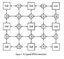
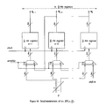
- a typical FPGA structure consists of a two-dimensional array of configurable logic elements connected by a configurable interconnection network, such as shown in FIG. 1 .
- FIG. 1 shows a networked structure, where the configurable logic blocks (CLBs) are the configurable functional elements, and the switches “S” are the configurable elements in the interconnection network.
- CLBs configurable logic blocks
- S switches
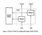
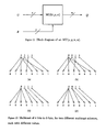
- the Xilinx Virtex-5 FPGA's CLBs each contain two elements known as slices.
- the most basic functional element in an FPGA usually consists of some combination of one or more Look-Up Tables (LUTs), combinational logic gates, flip-flops, and other basic logic elements.
- LUTs Look-Up Tables
- each slice contains four 64 ⁇ 1 LUTs, four flip-flops, an arithmetic and carry chain, and several multiplexers used to combine the outputs of the LUTs.
- the CLBs in an FPGA are also interspersed with other functional units, such as small memory blocks, other adder chains, and multipliers.
- a CLB can contain many configurable switches. Notwithstanding variations in FPGA terminology, we will use the term “CLB” to denote the basic unit represented in FIG. 2 .
- the FPGA's interconnection network is typically a two-dimensional mesh of configurable switches. As in a CLB, each switch S represents a large bank of configurable elements. The state of all switches and elements within all CLBs is referred to as a “configuration” of the FPGA. Because there is a large number of configurable elements in an FPGA (LUTs, flip-flops, switches, etc.), a single configuration requires a large amount of information. For example, the Xilinx Virtex-5 FPGA with a 240 ⁇ 108 array of CLBs requires in the order of 79 million bits for a single full configuration. The FPGA's CLBs are fine-grained functional elements that are incapable of executing instructions or generating configuration bits internally.
- configuration information must come from outside the chip.
- a limited amount of configuration information can be stored in the chip as “contexts;” however, given the limited amount of memory available on an FPGA for such a purpose, an application may require more contexts than can be stored on the FPGA.
- configuration information must still come from outside the chip, and the pin limited input can have severe consequences for the time needed for reconfiguration.
- Dynamic reconfiguration has two main benefits.
- a dynamically reconfigurable architecture can reconfigure between various stages of an application to use its resources efficiently at each stage. That is, it reuses hardware resources more efficiently across different parts of an algorithm. For example, an algorithm using two multipliers in Stage 1 and eight adders in Stage 2 can run on dynamically reconfigurable hardware that configures as two multipliers for Stage 1 and as eight adders for Stage 2. Consequently, this algorithm will run on hardware that has two multipliers or eight adders, as opposed to a non-configurable architecture that would need two multipliers and eight adders.
- the second benefit of dynamic reconfiguration is a fine tuning of the architecture to exploit characteristics of a given instance of the problem. For example in matching a sequence to a given pattern, the internal “comparator” structure can be fine-tuned to the pattern. Further, this tuning to a problem instance can also produce faster solutions.
- Dynamic reconfiguration requires a fast reconfiguration scheme. Because of this, partial reconfiguration is normally performed where only a portion of the FPGA is reconfigured. Partial configuration involves selecting the portion of the FPGA requiring reconfiguration (the addresses) and inputting the necessary configuration bits. Due to pin limitation, only a very coarse selection of addresses is available in a given time increment, resulting in a still substantially large number of FPGA elements being selected for reconfiguration. This implies that elements that do not need to be reconfigured must be “configured” anyway along with those that actually require reconfiguration.
- the information entering the chip can be classified into two categories: (a) selection and (b) configuration.
- the selection information contains the addresses of the elements that require reconfiguration, while the configuration information contains the necessary bits to set the state of the targeted elements.
- FPGAs are typically divided into sets of frames, where a frame is the smallest addressable unit for reconfiguration.
- a frame is typically one or more columns of CLBs.
- every CLB in a frame would be reconfigured, regardless of whether or not the application required them to be reconfigured. This can result in a “poorly-focused” selection of elements for reconfiguration, as more elements than necessary are reconfigured in each iteration. This implies that a large number of bits and a large time overhead are spent on the reconfiguration of each individual frame. If the granularity of selection is made finer, i.e., if fewer CLBs are in each frame, then the number of selection bits needed to address the frames increases by a small amount while the number of configuration bits for each frame decreases.
- word we use the term “word” to mean a set of bits. Different words may have different numbers of bits. We also use the terms “string” and “signal” synonymously with “word.”
- the O( ⁇ ) notation indicates an upper bound on the “order of” and is used to describe how the size of the input data affects resources (time, cost etc.) in an algorithm or hardware.
- a partition of set A is a division of the elements of the set into disjoint non-empty subsets (or blocks).
- a partition ⁇ with k blocks is called a k-partition.
- a 3-partition of the set ⁇ 8, 7, 6, 5, 4, 3, 2, 1, 0 ⁇ is ⁇ 7, 6, 5, 4 ⁇ , ⁇ 3, 2 ⁇ , ⁇ 1, 0 ⁇ , Partitions have no imposed order.
- An ordered k-partition is a k-partition ⁇ S o , S l , . . . , S k ⁇ 1 ⁇ with an order (from 0 to k ⁇ 1) imposed on the blocks.
- An ordered partition will be denoted ordered list of blocks .
- a 2-partition ⁇ S o , S 1 ⁇ may be ordered as S 0 , S l or S 1 , S 0 and S 0 , S 1 ⁇ S 1 , S 0 .
- a useful operation on partitions is the product of two partitions.
- ⁇ 1 and ⁇ 2 be two (unordered) partitions (not necessarily of the same size).
- an n-bit output can be viewed as a subset of an n-element set.
- Z n ⁇ 0, 1, . . . , n ⁇ 1 ⁇ .
- A n-bit signal
- the n-bit string A is called the characteristic string of the above subset.
- log n the base of all logarithms is 2. Consequently, we will write log n to indicate log 2 n. We will also use the notation log ⁇ n to denote (log n) ⁇ .
- Prior art methods to address the pin limitation problem include: (1) multiplexing, (2) storing information within the design, and (3) decoding.
- Multiplexing refers to combining a large number of channels into a single channel. This can be accomplished in a variety of ways depending on the technology. Each method assumes the availability of a very high speed, high bandwidth channel on which the multiplexing is performed. For example, in the optical domain, wavelength division multiplexing allows multiple signals of different wavelengths to travel simultaneously in a single waveguide. Time division multiplexing requires the multiplexed signal to be much faster than the signals multiplexed. Used blindly, this is largely useless in the FPGA setting, as it amounts to setting an unreasonably high clocking rate for parts of the FPGA.
- Decoders are the third means used to address the pin limitation problem.
- a decoder is typically a combinational circuit that takes in as input a relatively small number of bits, say x bits, and outputs a larger number of bits, say n bits, according to some mapping; such a decoder is called an “x-to-n decoder.” If the x inputs are pins to the chip and the n outputs are expanded within the chip, a decoder provides the means to deliver a large number of bits to the interior of the chip.
- An x-to-n decoder (that has x input bits) can clearly produce no more than 2 x output sequences, and some prior knowledge must be incorporated in the decoder to produce a useful expansion to n output bits.
- Decoders have also been used before with FPGAs in the context of configuration compression, where dictionary based or statistical schemes are employed to compress the stream of configuration bits.
- Our invention when used in the context of FPGAs has more application in selecting parts of the chip in a more focused way than conventional decoders do.
- the method we propose is a general decoder for any scheme employing fixed size code words, that decode into (larger) fixed size target words.
- the set of outputs produced by an x-to-n decoder can be represented as a set of (at most 2 x ) subsets of Z n .
- Sets S 0 , S 1 , S 2 and S 3 represent different decoders, each producing subsets of Z n .
- S 0 corresponds to the set of subsets ⁇ 0 ⁇ , ⁇ 1 ⁇ , ⁇ 2 ⁇ , . . . ⁇ 7 ⁇ . This represents the 3-to-8 one-hot decoder.
- a one-hot decoder causes severe problems if, in an array of n elements, some arbitrary pattern of those elements is needed for reconfiguration. Here, selecting an appropriate subset can take up to ⁇ (n) iterations. Notwithstanding this inflexibility, one-hot decoders are simple combinational circuits with a low O(n log n) gate cost (typically given as the number of gates) and a low O(log n) propagation delay. The one-hot decoder will usually take multiple cycles or iterations to set all desired elements to the desired configuration. Thus, reconfiguration is a time consuming task in current FPGAs and consequently, they fail to fully exploit the power of dynamic reconfiguration demonstrated on theoretical models.
- Look-up tables can function as a “configurable decoder.”
- a 2 x ⁇ n LUT is simply a (2 x )-entry table, where each entry has n bits. It can produce 2 x independently chosen n-bit patterns that can be selected by an x-bit address.
- LUTs are highly flexible as the n-bit patterns chosen for the LUT need no relationship to each other.
- this “LUT decoder” is also costly; the gate cost of such a LUT is O(n2 x ).
- O(n log n) For a gate cost of O(n log n), a LUT decoder can only produce O(log n) subsets or mappings. To produce the same number of subsets as a one-hot decoder, the LUT decoder has O(n 2 ) gate cost. Clearly, this does not scale well.
- the invention includes a reconfigurable mapping unit that is a circuit, possibly in combination with a reconfigurable memory device.
- the circuit has as input an x-bit word having a value at each bit position, and a selector bit word, input to the circuit.
- the circuit outputs an n-bit word, where n>x, where the value of each bit position of the n-bit output word is based upon the value of a pre-selected hardwired one of the bit positions in the x-bit word, where said hardwired pre-selected bit positions is selected by the value of the selector bit word.
- the invention may include a second reconfigurable memory device that outputs the z-bit word, based upon an input x-bit word to the second memory device, where x ⁇ z.
- the invention may produce the output n bit, a bits at a time.
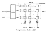
- FIG. 1 shows the structure of a typical field-programmable gate array (FPGA).
- FPGA field-programmable gate array
- FIG. 2 shows a block diagram of the Xilinx Virtex 5 configurable logic block.
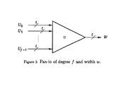
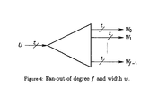
- FIG. 3 shows a block diagram for the function of a fan-in of degree f and width w.
- FIG. 4 shows a block diagram for the function of a fan-out of degree f and width w.
- FIG. 5 illustrates the typical implementation of a one-hot decoder though a 4-to-16 one-hot decoder.
- FIG. 6 illustrates the typical implementation of a multiplexer through a 4-to-1 multiplexer.
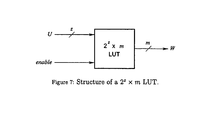
- FIG. 7 shows the block diagram of a 2 z ⁇ m LUT.
- FIG. 8 shows an implementation of a 2 x ⁇ m LUT.
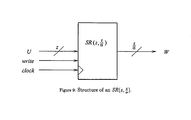
- FIG. 9 shows the structure of the shift register
- FIG. 10 shows one way to implement a shift register
- SR ⁇ ( z , z ⁇ ) that can be used as a serial-to-parallel and parallel-to-serial converter.
- FIG. 11 shows a block diagram of a mapping unit MU(z, y, n, ⁇ ).
- FIG. 12 shows an example with two different multicasts of 4 bits to 8 bits. Each multicast is further illustrated with different values for the 4-bit source word.
- FIG. 13 shows the general structure of a mapping unit MU(z, y, n, ⁇ ).
- FIG. 14 shows a fixed mapping unit MU(4, 1, 8, 1) that produces the set of subsets S 0 and S 1 of Table 2.
- FIG. 15 shows a fixed mapping unit MU(4, 2, 8, 1) that produces all three sets of subsets of Table 2.
- FIG. 16 shows the butterfly network, configured to illustrate the example permutation used in the discussion of post-permutation in mapping units.
- FIG. 17 shows an implementation of a bit-slice mapping unit MU(z, y, n, ⁇ ).
- FIG. 18 shows the structure of a mapping-unit-based configurable decoder MUB(x, z, y, n, ⁇ ).
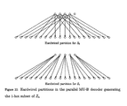
- FIG. 21 shows a parallel MU-B decoder that generates the one-hot subsets of Z n .
- FIG. 22 shows the hardwired partitions used in the two parallel MU-B decoders in an optimal configuration generating the 1-hot subset of Z n .
- FIG. 24 shows a general structure of a parallel MU-B decoder MUB(x, z, y, n, ⁇ , P).
- FIG. 25 shows a serial MU-B decoder variant.
- FIG. 26 shows a conceptual view of a recursive bit-slice mapping unit.
- ⁇ i ⁇ 0 ⁇ 1 . . . ⁇ i ⁇ 1 .
- the invention includes a mapping unit, and a configurable decoder that incorporates a mapping unit.
- the mapping unit may be an integral or bit-slice mapping unit.
- the invention includes configurable decoder variants and methods to construct the partitions required to configure a mapping unit. We will compare the invention to existing circuits, where the comparison is in terms of performance parameters (such as circuit delays and circuit costs, as measured by the number of overall gates in a design). All parameters are expressed in terms of their asymptotic complexity to avoid minor variations due to technology and other implementation-specific details.
- each instance of a gate has constant fan-in, constant fan-out, unit cost and unit delay; the fan-in and fan-out are each assumed to be at least 2 and here constant means independent of problem size. While the cost and delay of some logic gates (such as XOR) is certainly larger than the size and delay of smaller logic gates (such as NAND in some technologies), the overall number of gates in the circuit and the depth of the circuit provide a better measure of the circuit's costs and delays, rather than factors arising from choices specific to a technology and implementation.
- the delay or time cost of a combinational circuit is the length of the longest path from any input of the circuit to any output.
- the gate cost (or simply cost) of a circuit is the number of gates (AND, OR, NOT) in it. Clearly, the use of other gates such as NAND, XOR, etc. will not alter the gate cost expressed in asymptotic notation.
- a decoder is a combinational circuit (with the exception of the bit-slice units later described), that, in order to achieve a greater degree of flexibility, can be combined with look-up tables (LUTs), to create a configurable mapping unit or a configurable decoder. While LUTs could be implemented using sequential elements, for this work, LUTs are functionally equivalent to combinational memory such as ROMs. Any type of memory could be used for a LUT.
- any x-to-n decoder (including the mapping unit) takes x bits as input and outputs n bits, and the set of subsets generated by the configurable mapping unit decoder are those tailored in part for the application at hand. Different applications require different sets of subsets of Z n , and do so with different constraints on speed and cost.
- the reconfigurable mapping unit and configurable decoder have a portion of the hardware that can be configured (off-line) to modify the output bit pattern. This allows one to freely select a portion of the subsets produced by the mapping unit or reconfigurable decoder. Hence, given an understanding of the problem to be addressed, the mapping unit and/or configurable decoder may be configured to address the specific problem.
- an x-to-n decoder produces a set S of subsets of Z n .
- ⁇ the number of elements in S
- ⁇ the total number of subsets produced by the decoder.
- ⁇ 2 x the decoder allows some of the ⁇ subsets to be chosen arbitrarily (the independent subsets) while other subsets are set by prior choices (the dependent subsets).
- S ⁇ S′ denote the portion of subsets that can be produced independently by the decoder. For instance, in a LUT decoder, all entries are independent, while in a fixed decoder (non-configurable) there are no independent subsets.
- Basic circuit hardware is used as building blocks, in particular fan-in and fan-out circuits, one-hot decoders, multiplexers, look-up tables (LUTs), shift registers, and modulo- ⁇ counters. A brief explanation of each follows:
- a fan-in operation combines f signals into a single output, while a fan-out takes a single input signal and generates f output signals.
- the fan-in and fan-out operations are as follows:
- U 0 , U 1 , . . . , U f ⁇ 1 be f signals, each z bits wide.
- the operator o is an associative Boolean operation, such as AND, OR, NOR, etc. Diagrammatically, FIG. 3 shows a fan-in operation.
- FIG. 4 shows a fan-out operation.
- Fan-in and fan-out circuits of degree f and width z can be constructed with a gate cost of O(fz) and a delay of O(log f).
- a x-to-n decoder is a (usually combinational) circuit that takes x bits of input and produces n bits of output, where x ⁇ n.
- a decoder is used to expand an input from a small (2 x -element domain to an output from a large (2 n )-element set.
- Decoders can be divided into two broad classifications: (a) fixed decoders, which are inflexible, and (b) configurable decoders, where the set of subsets produced can be changed (or reconfigured) in some manner (typically off-line).
- One typical fixed decoder is the one-hot decoder.
- each of the n-bit output patterns has only one active bit (usually with a value of ‘1’), all other bits being inactive (usually ‘0’).
- Such a decoder is exemplified by set S 0 in Table 1. This decoder, in effect, selects one element at a time.
- a one-hot decoder also has a select input that allows the output set to be null.
- the one-hot decoder is used so often that the term “decoder” in the context of combinational circuits is usually taken to mean a one-hot decoder.
- a typical implementation of one-hot decoder is shown for a 4-to-16, one-hot decoder in FIG. 5 .
- an x-to-2 x one-hot decoder has a delay of O(x) and a gate cost of O(x2 x ).
- a multiplexer or MUX is a combinational circuit that selects data from one of many inputs and directs it to a single output line.
- a 2 x -to-1 multiplexer or a (2 x )-input multiplexer takes 2 x data inputs and using x control bits, selects one of the 2 x inputs as the output.
- FIG. 6 An example of a typical implementation of a multiplexer with four inputs is shown in FIG. 6 .
- each of the four data inputs, U 0 , U 1 , U 2 and U 3 is selected via an AND gate and a combination of the two control bits V 0 and V 1 , much like the one-hot decoder.
- a 2 x -to-1 multiplexer can be implemented as a circuit with a gate cost of O(x2 x ) and a delay of O(x).
- a 2 x ⁇ m LUT is a storage device with m2 x storage cells organized as 2 x words, each m bits long; see FIG. 7 .
- This LUT has as input x bits to address the 2 x locations and outputs an m-bit word.
- LUTs have a variety of other applications, such as implementing small logic functions.
- a 2 x ⁇ m LUT can implement any m Boolean functions, each of x variables, by storing their truth tables. This use of LUTs is quite common for implementing Boolean functions in FPGAs.
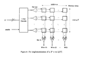
- LUTs can be implemented in a variety of ways, all LUTs require the same two components: a memory array and a method of addressing a word in the memory array.
- One possible method of addressing the LUT is to use an x-to-2 x one-hot decoder. The output of the one-hot decoder activates a wordline and enables the outputs of the memory storage cells. Each of the memory storage cell outputs are then fanned-in to form an m-bit output word. See FIG. 8 .
- the implementation shown in this figure is independent of the choice of memory storage elements. SRAM-based LUTs are perhaps the most common implementation; however, with minimal modifications, this basic design can easily accommodate other memory cell types.
- LUTs composed of sequential elements are also possible, however this would require the use of a clock.
- This clock can be independent of any other clock in the system.
- the asymptotic cost of the structure is unchanged; choices in memory technology only alter the size and access times of the LUT by a constant factor.
- the LUT will be a combinational element for cost analysis.
- a 2 x ⁇ m LUT can be implemented as a circuit with a gate cost of O(2 x (x+m)) and a delay of O(x+log m).
- FIG. 9 diagrams the operation.
- the shift register can also be configured as a parallel-to-serial converter. That is accept z/ ⁇ , bits during each cycle, and output an n-bit word every ⁇ cycles.
- FIG. 10 is a circuit implementation of such a shift register.
- SR ⁇ ( z , z ⁇ ) can be realized as a circuit with a gate cost of O(z) and a constant delay between clock cycles.
- Modulo- ⁇ Counter For any ⁇ >1, a modulo- ⁇ (or mod- ⁇ ) counter increments its output by ‘1’ every clock cycle, returning to ‘0’ after a count of ⁇ 1. Modulo- ⁇ counters are well known in the art.
- a modulo- ⁇ counter can be realized as a circuit with gate cost O(log 2 ⁇ ) and a delay of O(log log ⁇ ).
- the base unit of the invention is the mapping unit, and its features are diagrammed in FIG. 11 .
- the mapping unit MU(z, y, n, ⁇ ) can be viewed as a type of decoder: it takes in a small number of bits (z bits) and expands them to a larger number of bits (n bits), where typically z ⁇ n.
- z bits small number of bits
- n bits typically z ⁇ n.
- the mapping unit accomplishes the expansion of the z-bit source word to the n-bit output word by “multicasting” the z-bits to n places.
- a multicast of z bits to n bits is a one-to-many mapping from the z source bits to the n output bits, such that each output bit is mapped onto from exactly 1 source bit, but each source bit may map to 0, 1 or more output bits.
- the multicast operation typically transfers the value of a source bit to the output bit it is mapped to. Here we will use it in a more general sense in that the output bit derives its value from the source bit it is mapped from, for example by complementation. Unless we note otherwise, a multicast transfers the value of each source bit to its corresponding output bits. (The inclusion of parameters y and ⁇ in the mapping unit MU(z, y, n, ⁇ ) will be described later).
- a fixed mapping of 4 to 8 bits can be represented as a 4 to 8 multicast, and is diagrammed in FIG. 12( a )-( d ), where FIG. 12( a ), ( b ) represent one fixed multicast operation while FIGS. 12( c ) and ( d ) represent a second fixed multicast operation.
- mapping unit of the invention is broader than a unit containing one fixed multicasting operation. It uses several fixed multicasts, and the choice of the multicast operation to be employed is selected by the value of the y-bit selector address input to the mapping unit, as shown in FIG. 11 . Hence, the number of possible multicasts used in a MU(z, y, n, ⁇ ) is 2 y .
- Another characterization of a multicast is in terms of an ordered partition.
- the ordered partition represents the mapping of the source word bits to the output word bits, where the position of the block in the partition (for instance block ⁇ 7, 5, 3, 2 ⁇ is in position 4 of ⁇ right arrow over ( ⁇ ) ⁇ 1 ) represents the position of the source word bit (position 4 here), and the value of the block ( ⁇ 7, 5, 3, 2 ⁇ here) represents the output word bit positions to which the value of the input bit get mapped or cast into (here a(4) gets mapped to b(7), b(5), b(3) and b(2)).
- a mapping unit can be considered a mapping of a z-bit source word to an n-bit output word, using an ordered partition selected by the selector address (y bits), or a mapping ⁇ : Z 2 z ⁇ Z 2 y ⁇ Z 2 n .
- MU(z, y, n, ⁇ ) accepts as input a z-bit source word, U, and an ordered partition ⁇ right arrow over ( ⁇ ) ⁇ (one among 2 y ) as selected by the y-bit selector address, B, of FIG. 11 , and produces as output an n-bit output word (or a subset of Z n ).
- the source word could assume any value from ⁇ 0, 1 ⁇ z .
- the set of 2 y ordered partitions is fixed (usually hardwired in the mapping unit) and/or configured into a LUT internal to the mapping unit.
- a mapping unit is a decoder that accepts as input a z-bit source word u and an ordered z-partition ⁇ right arrow over ( ⁇ ) ⁇ of an n-element set (specified in terms of a y-bit selector address). It produces an n-bit output word.
- Mapping units can be classified as integral or bit-slice.
- An integral mapping unit generates all n output bits simultaneously and (for reasons explained below) has the parameter ⁇ set to 1.
- a bit-slice mapping unit generates the n output bits in a rounds; i.e., n/ ⁇ bits at a time.
- One could view the integral mapping unit as a bit-slice mapping unit with ⁇ 1.
- mapping units can be general or universal. In informal terms, a universal mapping unit can produce any subset. Fixed mapping units cannot be universal (unless n is very small or a very high cost can be accepted).
- a general structure of a mapping unit, MU(z, y, n, ⁇ ), is as shown in FIG. 13 .
- the n-bit output word comes from a bank of n multiplexers (MUXs).
- MUX i (where 0 ⁇ i ⁇ n) accepts 2 yi data bits as input and uses y i control bits.
- Each data input of a MUX is hardwired from one of the z source bits. This relationship between the source word and MUX inputs is fixed at the time of manufacture (even for configurable mapping units); although, in principle, some amount of configurability may be introduced in these connections.
- the concatenated control bits B 0 , B 1 , . . . , B n ⁇ 1 is called the selector word of the mapping unit.
- the selector word can be of different sizes and can be generated in a variety of ways in different types of mapping units.
- the mapping unit has, embedded in its structure, room for 2 y different selector words, each corresponding to an ordered partition (or a multicast scheme from the source word to the output word). These selector words are generated and chosen by the selector module, using a y-bit selector address.
- control bits can be derived in any manner from the y selector address bits, for example, by directly hardwiring a subset of the y bits to each MUX control. At the other extreme is using a LUT for the selection module with wordsize w such that
- mapping units fixed and configurable. Other types and variants are described later.
- mapping unit When the ordered partitions of a mapping unit are fixed (as in an FMU), it can be shown that certain subsets cannot be produced.
- CMU configurable mapping unit
- the selector module is a 2 y ⁇ ny LUT (called the configuration LUT).
- the values stored in the LUT are completely unconstrained.
- a configurable mapping unit MU(z, y, n, ⁇ )
- MU(z, y, n, ⁇ ) can be realized as a circuit having a gate cost of O(ny2 y ) and a delay of O(y+log n).
- the configurable mapping unit There are two important properties of the configurable mapping unit. The first is that from a perspective outside of the mapping unit, nothing changes between a fixed mapping unit and a configurable mapping unit; that is, to produce a desired subset S j i , the same values are needed for signals U and B in a configurable mapping unit as they are in a fixed mapping unit. The second is that each “grouping” of the y control bits (each corresponding to a particular MUX) in the ny-bit selector words has the same value in an FMU; If this value is v, then each of the n output bits is derived from the ordered partition ⁇ right arrow over ( ⁇ ) ⁇ v . However, this does not have to be the case in a CMU.
- a word in the LUT illustrated in Table 3 could have the value 00 01 10 11 00 01 10 11; this is a combination of values of different ordered partitions for different MUXs.
- bits 7, 6 and 5 of the 8-bit output word would be derived from ⁇ right arrow over ( ⁇ ) ⁇ 0 , ⁇ right arrow over ( ⁇ ) ⁇ 1 and ⁇ right arrow over ( ⁇ ) ⁇ 2 , respectively, as 00, 01 and 10 are the binary representations of 0, 1 and 2, respectively. This would result in multicast with the ordered partition ⁇ 7, 6, 3, 1 ⁇ , ⁇ 4, 2 ⁇ , ⁇ 0 ⁇ , ⁇ 5 ⁇ .
- the main function of the mapping unit is to convert a set of source words into a set of output words that correspond to a given set S of subsets of Z n . In order to achieve this we consider two scenarios.
- an ordered partition is an abstract representation of a multicast from the source word to the output word. It is possible for different source words to use the same ordered partition to generate different output words (or subsets). Ideally, the 2 z source words and 2 y (ordered partition) selector words should produce 2 z+y distinct output words, each of which must be one of interest to us. This requires a careful selection of ordered partitions and source words.
- Procedure Part_Gbn a procedure that creates partitions (multicasts) for a mapping unit MU (z, y, n, ⁇ ).
- Procedure Part_Gbn a procedure that creates partitions (multicasts) for a mapping unit MU (z, y, n, ⁇ ).
- MU mapping unit
- S be a set of subsets of Z n that we wish the mapping unit to generate.
- the induced partition creates two blocks, one containing the bit positions that have a 0 value, and the other block containing the bit positions having a 1 value. For instance, if the subset is represented by the bit stream 10001100, then the induced partition is the 2-partition ⁇ 0, 1, 4, 5, 6 ⁇ , ⁇ 2, 3, 7 ⁇ , while if the input bit stream is 11111111, then the induced partition is the 1-partition ⁇ 0, 1, 2, 3, 4, 5, 6, 7 ⁇ . The induced partition is not an ordered partition.
- the procedure to create a set of z-partitions that generate a given set S of subsets of Z n is as follows. It assumes that the subsets of S are ordered in some manner. We indicate this by the symbol ⁇ right arrow over (S) ⁇ . At this stage it is not important how the subsets are ordered. We will assume that the indices of the elements of ⁇ right arrow over (S) ⁇ reflect their order. This order determines the order in which the algorithm will consider each subset and does not reflect how the partitions will be ordered.
- the partitions ⁇ 0 , ⁇ 1 , . . . are the outputs of Procedure Part_Gen.
- the basic idea of the procedure is to “add” subsets in the prescribed order into the current partition until the partition has too many blocks. Then it starts afresh with the next partition.
- the mapping unit uses these ordered partitions with values of the source words shown in Table 5 to generate each subset of S. Actually, the table illustrates the impact of two different orders on the partitions and is discussed later. For now, it suffices to observe the first set of 4 rows that apply to ⁇ right arrow over ( ⁇ ) ⁇ 0 that includes the subsets of S 0 .
- a subset can be generated in a variety of ways, as the same z-bit source word applied to different ordered partitions can result in the same value.
- two different source words applied to two differently ordered partitions can result in the same value.
- a subset not in S can also be produced.
- using the z-bit source word 1010 with the ordered partition ⁇ right arrow over ( ⁇ ) ⁇ 0 produces the output word 10111010 that corresponds to the subset ⁇ 7, 5, 4, 3, 1 ⁇ which is not in S.
- Subsets and their induced partitions may be repeated. For example, subsets S 3 0 and S 3 1 of the above example are equal, the above procedure ignores repeated subsets and their induced partitions in generating ordered partitions. However, partitions corresponding to classes of algorithms or specific applications may benefit from repeating subsets, that is, to include the repeats.
- a partition with fewer than z blocks, such as ⁇ 1 results in “don't care” values (d) for the bits not corresponding to any block in the partition.
- the subset S 1 1 with source word d011 may be produced from the source word 0011 or 1011.
- the conversion of an unordered partition to an ordered partition can be done in as many z! ways. Some of these may be more advantageous than others.
- An ordering that results in common source words used to produce the subsets of S i and S k (corresponding to different ordered partitions) can be useful when the mapping unit is used as part of a larger design. This is because the same z-bit source words can be used to produce both S i and S k .
- Table 5 demonstrates two ordered partitions for S 0 and S 1 , resulting in two sets of source words for each set.
- mapping unit MU(z, y, n, ⁇ ) can generate a number of independent subsets ⁇ 2 y ⁇ log z ⁇ , provided 2 y log z ⁇ 2 x . If the partitions are fixed and z+y ⁇ n, then it can be proved that the number of independent subsets is 0.
- mapping unit that uses C values from ⁇ 0, 1, . . . , 2 z ⁇ 1 ⁇ as source words and Y ⁇ 2 ⁇ ordered partitions to produce CY distinct subsets. That is, it is possible to construct a mapping unit with z+y bits of input (where
- G j denote the set of source word bits that have been hardwired to one of the data inputs of the MUX at position j.
- the multiplexers at output position 4 is connected to source word positions 1, 2 and 3.
- output position 5 (resp., 6) is connected to source word positions 0 and 3 (resp., 2 and 3).
- H B ⁇ j ⁇ B ⁇ G j .
- a partition ⁇ is said to be realizable on a set of hardwired connections between the source word and MUX inputs if and only if there exists for each output position j, an assignment of a source word position i j , such that for any two output bit positions 0 ⁇ j, j′ ⁇ n in (not necessarily distinct) blocks.
- B and B′ of ⁇ are said to be realizable on a set of hardwired connections between the source word and MUX inputs if and only if there exists for each output position j, an assignment of a source word position i j , such that for any two output bit positions 0 ⁇ j, j′ ⁇ n in (not necessarily distinct) blocks.
- the hardwired connections support a multicast from source word bit i j to output position j. Since i j is unique to the block containing j, the multicast is restricted to be within a block. In fact, the indices i j convert ⁇ into the ordered partition if.
- a given partition may not be realizable on a set of hardwired connections. Is it possible to check if a given partition IT is realizable, and if so, order it accordingly?
- a matching on the graph is a set of edges of the graph such that no two edges are incident on the same node.
- a matching is a maximum matching, if no other matching has more edges than it.
- a simple method to impose a realizable order (if one exists) on an unordered partition is to find a maximum matching for its graph. If it has k edges (k is the number of blocks in ⁇ ), then use it as indicated above to order ⁇ . If the matching has less than k edges, then no k-edge maximum matching exists and ⁇ is not realizable on the set of hardwired connections. Standard polynomial-time algorithms exist for maximum matchings on a bipartite graph.
- B be a block of a partition ⁇ .
- H B tends to decreases in size.
- H B it is possible for H B to be empty, in which case the partition is clearly not realizable.
- hardwired connections were random, a good strategy would be to construct, partitions whose blocks have roughly the same size. This could be a guiding principle for the algorithm. If the hardwired connections follow some pattern, then that information could be used to develop a heuristic to select partitions with small blocks.
- Procedure Part_Gen In the first phase we examine different orders for the elements of the given set S (that is, we consider different ⁇ right arrow over (S) ⁇ ), then call Procedure Part_Gen collecting as many large partitions (with “nearly” z-blocks) as possible. Between each call to Procedure Part_Gen, we remove the subsets accounted for so far from S. The orders considered in this phase may be based on some knowledge of the subsets to be generated.
- the second phase is based on the observation that a partition with fewer blocks has a higher likelihood of being realizable.
- this phase we repeat the processing in the first phase, this time calling Procedure Part_Gen with different values for the second parameter that limits the number of blocks in a partition. That is, we try to construct a partition with many blocks, but will settle for one with few blocks, if necessary.
- the third phase is needed for those subsets S i ⁇ S for which ⁇ S i itself is not realizable.
- the third phase splits these subsets S i further with the aim of generating the elements of S i a few at a time. This is similar to the approach followed by bit-slice mapping units (described later). In the extreme case if S i is generated one element at a time, the strategy uses the same method currently followed in one-hot decoders.
- mapping unit at manufacture
- m l,j represent input l of multiplexer j.
- the aim is to assign each of these multiplexer inputs to one of the z source word bits s 0 , s 1 , . . . , s z ⁇ 1 .
- Map input m l,j to bit s q , where q (l+2 y j)(mod z).
- a set of q consecutive multiplexers have 2 y ⁇ (q ⁇ 1) common source word bits. If Q is a block of an unordered partition, then any of these common source word bits form H Q and can be used to assign the order of the block as indicated earlier.
- This post permutation can be achieved by a butterfly network whose switches are configurable 2-input multiplexers.
- This network has a O(n log n) gate cost and O(log n) delay; that would not significantly alter the cost of the mapping unit in most cases.
- the network can be configured as needed using standard permutation-routing algorithms for the butterfly network. It may also be possible to use a butterfly network with fewer than the standard 1+log n stages as permutations among proximate outputs may not be required. This would further reduce the cost of the butterfly network.
- the butterfly network is a blocking network (that is, certain permutations cannot be achieved).
- other (more expensive) non-blocking permutation networks can be employed to overcome this problem.
- mapping units While configurable mapping units provide more flexibility, they are more expensive than fixed mapping units. If the application does not call for such a flexibility, a fixed mapping unit may be preferable.
- two hybrid mapping units that use elements of both the fixed and variable mapping units and occupy a middle ground between the flexibility and cost of the fixed and configurable mapping units.
- these ny bits of MUX control come from the configuration LUT in a configurable mapping unit; here y selector address bits are used to address at most 2 y LUT locations, each ny bits long.
- the signals B 0 , B 1 , . . . , B n ⁇ 1 are completely independent of each other.
- Z n be the set of (indices of) MUXs in the mapping unit. Divide this set into two disjoint subsets F and R (in any convenient manner that may depend on the application area).
- Z n represent the set of MUXs in the mapping unit. For some integer 1 ⁇ l ⁇ n, partition Z n into E blocks; Let this partition be ⁇ R 0 , R 1 , . . . , R l ⁇ 1 ⁇ . (This partition has nothing to do with the partition of the outputs associated with the multicast from the source word bits.)
- both hybrids reduce the size of the LUT word to ly ⁇ ny. This reduces the cost of the LUT if its size is kept the same. Alternatively, this can also allow one to increase the number of words in the LUT for the same cost as in the configurable mapping unit. An implication of this is that the configuration LUT can now store more partitions (say 2 y′ /partitions for some y′>y) for the same cost as the configurable mapping unit. This would require y′ bits to be input to the configuration LUT.
- each MUX (regardless of whether it is in F or R) would still use y control bits and, consequently, we would still hardwire only 2 y source word bits to each MUX. This is needed to keep the collective cost of the n MUXs the same as before.
- the hybrid mapping units can be viewed as a generalizations of the fixed and configurable mapping units.
- a bit-slice mapping unit generates just part of the output subset (represented by an n-bit word) at a time. It constructs a subset over ⁇ iterations, generating n/ ⁇ bits in each iteration. This allows the mapping unit to exploit repeated patterns, such as these demonstrated in Table 6, representing two forms of reduction. Notice that to generate 8 words, each 16 bits long, only 6 words, each 4 bits long, need to be generated. For example, the subset S corresponding to word
- Subset S Repeated Patterns 1111111111111 1111 0001000100010001 0001 0000000100000001 0000, 0001 0000000000000001 0000, 0001 0000000011111111 0000, 1111 0000000000001111 0000, 1111 0000000000000011 0000, 0011 0000000000000001 0000, 0001 0001000100010001 can be constructed over 4 iterations using the bit pattern 0001. Overall, this allows the bit-slice mapping unit to decrease the required gate cost of its internal components in situations where an increased delay is tolerable.
- a shift register acts as a parallel to serial converter and stores the z-bit source words and outputs n/ ⁇ bits every ⁇ cycles to the internal mapping unit
- mapping unit ( n ⁇ ⁇ - ⁇ bit ) output of the mapping unit is stored in another shift register which parallelizes the
- a mod- ⁇ counter orchestrates this parallel to serial conversion by triggering a write-in operation on the input shift register and a write-out on the output shift register every a cycles. This allows a new source word to be input into the bit-slice mapping unit and an n-bit output q written out every a cycles.
- bit-slice mapping unit is a sequential circuit
- the clock delay of the circuit we assume that the clock delay of the circuit to be the longer of (a) the longest path between any flip-flop output and any flip-flop input and (b) the longest path between any circuit input and output.
- a bit-slice mapping unit MU(z, y, n, ⁇ ) can be realized in a circuit with a gate costs of
- bit-slice mapping unit shows good savings. In determining whether or not a bit-slice mapping unit is suitable to a design, a variety of considerations must be taken into account.
- mapping unit fixed, configurable, integral or bit-slice
- MU(z, y, n, ⁇ ) has the following parameters.
- a configurable decoder has the same basic functionality as a fixed decoder.
- An x-to-n configurable decoder accepts an x-bit input word and outputs up to 2 x outputs, each n bits wide. Unlike fixed decoders, the output of a configurable decoder is not fixed at manufacture. With configuration, the n-bit outputs can be changed to a different pattern of bits, thus supplying a degree of flexibility not present in fixed decoders.
- a 2 x ⁇ n look-up table or LUT may be considered as a type of x-to-n configurable decoder.
- a 2 x ⁇ n LUT also takes in an x-bit input word and outputs up to 2 x words, each n bit wide, where the n-bit words are determined by the contents of the LUT's memory array.
- the configurable decoder described here is a circuit that uses a LUT (with a smaller order of cost), combined with a mapping unit.
- the mapping units we consider have the same order of cost as the LUT, and this allows the LUT cost to be kept as small as a fixed decoder while allowing a large number of n-bit subsets to be produced within the same order of gate cost as fixed decoders.
- These “mapping-unit-based” configurable decoders or MU-B decoders. They take the same forms as the mapping unit itself: be integral or bit-slice, fixed or configurable. It should be noted that the MU-B decoder is always configurable, as even one using a fixed mapping unit employs a LUT.
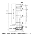
- FIG. 18 shows a block diagram of the mapping-unit-based decoder. To put the figure in perspective, x z ⁇ n, generally. Unlike the LUT decoder solution, this solution expands the x-bit input in stages to construct the n-bit output.
- the x-to-n MU-B decoder (denoted by MUB(x, z, y, n, ⁇ )) has two main components, a 2 x ⁇ z LUT and a mapping unit MU(z, y, n, ⁇ ).
- the LUT maps an x-bit input to a narrow z-bit word.
- the mapping unit MU(z, y, n, ⁇ ) accepts this z-bit LUT output as an input source word u. It also accepts an ordered partition if as indirectly selected by the y-bit selector word B).
- the MU(z, y, n, ⁇ ) then uses the operation ⁇ (u, ⁇ right arrow over ( ⁇ ) ⁇ ) to produce an n-bit word representative of a subset of Z n .
- Any MU(z, y, n, ⁇ ) in combination with a 2 x ⁇ z LUT (or other type of memory) is considered a type of MU-B decoder, MUB(x, z, y, n, ⁇ ) as shown in FIG. 18 .
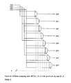
- the next example illustrates a MU-B decoder with a bit-slice mapping unit.
- MUB(x, z, y, n, ⁇ ) fixed mapping unit would require 16 multiplexers with 2 inputs each and a 5 ⁇ 5 LUT to hold the values of the source words (note that this is due to an intelligent ordering; in general the LUT could be as large as a 10 ⁇ 5).
- n ⁇ 4 ⁇ ⁇ bit bit words shown in Table 8.
- the LUT must still supply a z-bit word to the bit-slice mapping unit (which in this case may increase to a 6-bit word based on the rounding up of
- the implementation depends on the allowable costs, the number of z-bit source words and the corresponding size of the LUT, and the subsets that must be produced. Further, the ordering of the partitions can determine not only the size of the LUT in the MU-B decoder (and thus also the values of its parameters), but also dictate the subsets that can be produced.
- a mapping-unit-based configurable decoder MUB(x, z, y, n, ⁇ ) has a delay of O(x+log z+ ⁇ (y+log n)) and a gate cost of
- MUB(x, z, y, n, ⁇ ) can produce at least
- a MUB(x, z, y, n, ⁇ ) can be built that produces 2 x+y distinct subsets of Z n .
- the MU-B decoder is more flexible, generating more subsets than the LUT decoder.
- FIG. 19 Consider the binary tree reductions (or simply binary reductions), shown in FIG. 19 .
- the number of resources is reduced by a factor of two in each level of the tree;
- FIGS. 19( a ) and ( b ) illustrate this for two particular reductions.
- the bit patterns representing these reductions are also shown, where a bit has a value of ‘1’ if it survives the reduction at a particular level in the tree and a value of ‘0’ if it does not.
- S i the subset of Z n used during iteration i of a binary reduction (where 0 ⁇ i ⁇ log n) by S i .
- a MUB(log log 2n, log 2n, y, n, ⁇ ) can implement 2 y /different binary reductions. Since corresponding subsets in different binary reductions still have the same number of elements, the same set of log 2n source words can be used for all reductions; different ordered partitions need to be used, however.
- the output set (represented as an n-bit word with bit 0 as the lsb) produced by source word s 3 , s 2 , s 1 , s 0 and the ordered partition is s 3 , s 2 , s 3 , s 1 , s 3 , s 2 , s 3 , s 0 .
- a set of one-hot subsets is a set of subsets of Z n , each represented by an n-bit output word with each output word having only one active bit (usually with a value of ‘1’), all other bits being inactive (usually ‘0’).
- Table 10 shows an example for active-high logic.
- the 1-hot sets are easy to produce in a conventional fixed decoder, they present a difficult embodiment for the MU-B decoder described so far.
- a LUT contains a 1-hot address decoder, and since a configurable decoder MUB(log n, z, y, n, ⁇ ) contains a n ⁇ z LUT, a simple switch allowing the output of the LUT's address decoder to be the output of the configurable decoder automatically allows the configurable decoder to produce the 1-hot subset.
- the parallel decoder described subsequently teaches a simple way to construct a one-hot decoder out of MU-B decoders.
- the subsets of the Ascend/Descend class of communications are more difficult than those of the binary reduction for a mapping unit to produce. This is because the product of all induced partitions of the 2 log n subsets of the Ascend/Descend class of communications results in an n-partition of Z n as in the one-hot case; again as z ⁇ n, this cannot be represented by a single z-partition. However, the partitions induced by ASCEND/DESCEND subsets can be combined more effectively.
- ASCEND/DESCEND subsets are in complementary pairs that induce the same partition.
- each level of the ASCEND/DESCEND algorithm has one complementary pair; that is, there one induced partition per level of the algorithm.
- log z such levels
- log z 2 log z source words can produce 2 log z of the different 2 log n subsets.
- Table 11 illustrates a possible ordering of the partitions and source words for the ASCEND/DESCEND sets shown in FIG. 20 .
- Decoders can be structured in a parallel configuration utilizing a merge operation (such as an associative Boolean operation) to combine the outputs of two or more decoders.
- a parallel embodiment using MU-B decoders will be denoted MUB(x, z, y, n, ⁇ , P) where the parameter P denotes the number of configurable decoders connected in parallel.
- a parallel configurable decoder can produce sets of subsets of Z n not easily produced by the configurable decoders previously presented.
- the following example demonstrates the use of parallel decoders to produce the one-hot decoder.
- q i,0 and q i,1 are subsets of Z n .
- ⁇ 1 ⁇ q j , 1 ⁇ : ⁇ 0 ⁇ j ⁇ n m ⁇ , respectively.
- S 1 ⁇ q j , 1 ⁇ : ⁇ 0 ⁇ j ⁇ n m ⁇ .
- two z-partitions of n can generate these subsets.
- each subset of S 0 and S 1 can be independently generated by different MU-B decoders, each using just one partition.
- q i,0 ⁇ q j,1 ⁇ jm+i ⁇ , and it can be shown that for each x ⁇ Z n , there exists unique values 0 ⁇ i ⁇ m and
- ?? ⁇ q i , 0 ⁇ q j , 1 : 0 ⁇ i ⁇ m ⁇ ⁇ and ⁇ ⁇ 0 ⁇ j ⁇ n m ⁇ is the set of one-hot subsets.
- a simple method to generate the one-hot subsets using parallel decoders is shown in FIG. 21 .
- both m and n/m form feasible values for the input for a mapping unit; that is,
- Both MU-B decoders use a single partition, hardwired into their respective mapping units, as shown in FIGS. 22( a ) and ( b ).
- each MU-B decoder is the cost of a ⁇ square root over (n) ⁇ square root over (n) ⁇ LUT with a
- FIG. 23 illustrates this. Since a conventional log n-to-n one-hot decoder has O(log n) delay and O(n log n) gate cost, decoders D i each has O(log n) delay and O( ⁇ square root over (n) ⁇ log n) gate cost.
- the last step of ANDing the two set of n bits clear las constant delay and O(n) gate cost. (Note if an active-low convention is adopted for the decoder, the above AND gates would be replaced by OR gates.)
- this implementation of a one-hot decoder has O(log n) delay and O(n) gate cost. Compared to the conventional implementation of a one-hot decoder exemplified in FIG. 5 , our design has comparable delay, but a lower order of cost. In fact, since n outputs are required, this asymptotic gate cost cannot be improved upon.
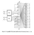
- a P-element parallel configurable decoder MUB(x, z, y, n, ⁇ , P) is shown in FIG. 24 .
- P decoders “receive” all x+y input bits.
- each decoder CD i where 0 ⁇ i ⁇ P, selects a portion x i and y i of the input bit streams x and y, respectively, as the input and selection information.
- MUB i and MUB j may use the same input bit(s) or share some common input bit(s) for their LUTs. Therefore, x i ⁇ x and
- ⁇ i 0 P - 1 ⁇ x i ⁇ x ,
- the (optional) control allows the merge unit to select from a range of options.
- each MUB i can produce its own independent set of n i -bit outputs.
- the manner in which these outputs combine depends on the merge unit. For example, let each MUB i produce an n-bit output (that is, a subset of Z n ) and let S i be the independent set of subsets produced by MUB i .
- the merge operations be ⁇ , an associative set operation with identity S o .
- Intersection, Union, and Ex-OR represent such an operation with Z n , 0/, and 0/, respectively, as identities. If each MUB i produces a set of subsets S i that includes S o , then the whole parallel MU-B decoder produces an independent set that includes
- ⁇ i 0 P - 1 ⁇ S i .
- MUB i have a delay of D i and a gate cost of G i . If D M and G M are the delay and gate cost of the merge unit, then the delay D and gate cost G of the parallel MU-B decoder MUB(x, Z, y, n, ⁇ , P) are
- D max ⁇ ( D i ) + D M + O ⁇ ( log ⁇ ⁇ P ) .
- the other variants of the MU-B decoder include a serial MU-B decoder and one based on a recursive bit-slice mapping unit. These variants are not preferred as they did not provide any additional benefit over the designs included by a stand alone mapping-unit-based decoder.
- a serial MU-B decoder is shown in FIG. 25 .
- Two or more mapping units are cascaded to construct the subsets of Z n .
- the independent subsets produced by the second mapping unit are dependent on what is provided to it, that is, the range of values of z 1 , which is in turn dependent on the number of independent subsets produced by the first mapping unit.
- the first mapping unit in FIG. 25 can produce 2 y0 (log z 0 ) independent subsets, where z 0 is a relatively small value
- a single LUT can usually subsume both the LUT and the first mapping unit in the serial variant, and be within the gate cost of the second mapping unit and provide more independent subsets.
- a recursive bit-slice mapping unit illustrated in FIG. 26 , where two or more bit slice mapping units are nested within one another, such that an input to the first bit-slice mapping unit is broken down by a factor of ⁇ 0 then broken down further by a factor of ⁇ 1 , and so on, until it reaches the lowest level mapping unit. It is then reconstructed to an n-bit output.
- this reconstruction requires a large number of shift registers and multiple clocks, and the linear reduction of cost does not provide additional benefit from that of a single bit-slice mapping unit.
- Typical sensor networks consist of a collection of small sensor nodes (motes) that communicate to a base station through a distributed wireless network. Because the range of individual nodes is small, outlying nodes must relay their data to the base station through closer nodes. A large amount of power is expended during the receiving and transmission of data. Because of this, data must be compressed or encoded in some fashion so as to conserve power. This situation is similar to the pin limitation problem, wherein a large amount of data must be compressed in some fashion to pass through a small number of I/O pins.
- a decoder-based solution to the pin limitation problem could easily be applied to sensor networks, as the decoder itself would require no significant changes to the architecture of the sensor and would act as a method of compression for the data.
- a configurable decoder (and a reverse encoder) can serve to reduce the number of bits transmitted between sensor nodes without requiring a drastic redesign of the sensor nodes.
- An external power controller can reduce the clock frequency of a chip such that the overall power consumed by the chip is reduced. Used indiscriminately, this method can unnecessarily hurt the performance of the chip, as not all parts of the chip may require a reduction in power.
- a “smart” power controller could select portions of a chip for reductions in power, reducing the performance of only those portions that are not necessary for the chip's current execution. Thus, the overall power draw of the chip would be reduced without drastically affecting the performance. However, this ability is hampered by the large number of I/O pins that would be necessary for such addressing.
- a decoder-based solution that would allow efficient addressing of portions of a chip through a small number of I/O pins would directly address this problem.
- this selection can be used by a smart agent that observes data from a collection of chips and issues commands to selectively power-down portions of these chips.
- a sharp focused selection (such as that afforded by the configurable decoder) could be useful in this environment.
Abstract
Description
B=b+Cα.
| TABLE 1 |
| Example of 3-to-8 Decoders |
| Decoder Inputs | S0 | S1 | S2 | S3 |
| 000 | 00000001 | 01010101 | 11111111 | 00001101 |
| 001 | 00000010 | 10101010 | 00001111 | 10010010 |
| 010 | 00000100 | 00110011 | 00000011 | 10100010 |
| 011 | 00001000 | 11001100 | 00000001 | 00111101 |
| 100 | 00010000 | 00001111 | 11110000 | 01001110 |
| 101 | 00100000 | 11110000 | 11000000 | 11010001 |
| 110 | 01000000 | 11111111 | 10000000 | 11100001 |
| 111 | 10000000 | 00000000 | 00111100 | 01111110 |
that can be used as a serial-to-parallel and parallel-to-serial converter.
as follows. It accepts as input a z-bit signal, and every clock cycle, outputs a
slice of that signal.
can be realized as a circuit with a gate cost of O(z) and a constant delay between clock cycles.
Modulo-α Counter: For any α>1, a modulo-α (or mod-α) counter increments its output by ‘1’ every clock cycle, returning to ‘0’ after a count of α−1. Modulo-α counters are well known in the art.
μ:Z 2
Here, some or all of the w bits in each selector word can be used to control a MUX.
| TABLE 2 |
| Example sets of subsets of Z8. |
| Sj i | S0 | S1 | S2 | ||
| S0 i | 11111111 | 11111111 | 10100010 | ||
| | 01010101 | 00001111 | 11111101 | ||
| | 00010001 | 00000011 | 01011010 | ||
| | 00000001 | 00000001 | 00000111 | ||
Configurable Mapping Unit:
| TABLE 3 |
| Configuration LUT words to produce the subsets of Table 2. |
| selector address | ny-bit selector word | Set |
| b ∈ B | in LUT | Si |
| 00 | 00 00 00 00 00 00 00 00 | |
| 01 | 01 01 01 01 01 01 01 01 | |
| 10 | 10 10 10 10 10 10 10 10 | |
| 11 | 11 11 11 11 11 11 11 11 | S3 |
itself. For example, when b=00, the LUT word is 00 00 00 00 00 00 00 00 corresponding to the ordered partition {right arrow over (π)}0 for set S0 (see Tables 2 and 4). Then with u=0111, we have the output word μ(u, {right arrow over (π)}0)=01010101. Similarly, with u=0011, we μ(u, {right arrow over (π)})=00010001. Thus, in this illustration, the selector address b=00 corresponds only to the ordered partition {right arrow over (π)} for S0.
-
- The mapping unit's hardwiring has already been fixed. The set of subsets that can be produced can be limited by this hardwiring between the source word and the MUX data inputs. Can a given S be produced by the mapping unit? If S can be produced, then what are the source words that produce the subsets? For a configurable mapping unit, what are the contents of the configuration LUT?
- Here we are designing the entire mapping unit, including the hardwired connections. How can we factor in an expected set of subsets into the design? If no set of subsets is given, what hardwired connections provide the flexibility to produce a large number of subsets?
| TABLE 4 |
| Partitions πS |
| Sj i | πS j 0 | πS j 1 | πS j 2 |
| S0 i | {{7, 6, 5, 4, 3, 2, 1, 0}} | {{7, 6, 5, 4, 3, 2, 1, 0}} | {{6, 4, 3, 2, 0}, {7, 5, 1}} |
| S1 i | {{7, 5, 3, 1}, {6, 4, 2, 0}} | {{7, 6, 5, 4}, {3, 2, 1, 0}} | {{1}, {7, 6, 5, 4, 3, 2, 0}} |
| S2 i | {{7, 6, 5, 3, 2, 1}, {4, 0}} | {{7, 6, 5, 4, 3, 2}, {1, 0}} | {{7, 5, 2, 0}, {6, 4, 3, 1}} |
| S3 i | {{7, 6, 5, 4, 3, 2, 1}, {0}} | {{7, 6, 5, 4, 3, 2, 1}{0}} | {{7, 6, 5, 4, 3}, {2, 1, 0}} |
πS
πS
πS
-
- 1. For each SiεS, compute its induced partition πS
i . - 2. Starting from π0, pick the largest integer l such that πS
0 πS1 . . . πSl−1 has ≦z blocks. Let π0=πS0 πS1 . . . πSl−1 . - 3: Starting from πl, pick the largest integer m such that πS
l πSl+1 . . . πSl+m−1 has ≦z blocks. Let π1=πSl πSl+1 . . . πSl+m−1 . - 4. Repeat this process until all induced partitions πS
i have been included in some πj.
- 1. For each SiεS, compute its induced partition πS
{right arrow over (S)}={S 0 0 ,S 1 0 ,S 2 0 ,S 3 0 ,S 1 1 ,S 2 1 ,S 0 2 ,S 1 2 ,S 2 2 ,S 3 2}.
(Note that S0 1, and S3 1 are not included as these are repeated elements). The induced partitions corresponding to each Sj i are in Table 4. Then using the Procedure Part_Gen we obtain
πS
πS
πS
πS
πS
πS
πS
{right arrow over (π)}0={{7,5,3,1},{6,2},{4},{0}},
{right arrow over (π)}1={{7,6,5,4},{3,2},{1,0}},
{right arrow over (π)}2={{7,5},{2,0},{6,4,3},{1}}.
The mapping unit uses these ordered partitions with values of the source words shown in Table 5 to generate each subset of S. Actually, the table illustrates the impact of two different orders on the partitions and is discussed later. For now, it suffices to observe the first set of 4 rows that apply to {right arrow over (π)}0 that includes the subsets of S0.
there exists a mapping unit that uses C values from {0, 1, . . . , 2z−1} as source words and Y≦2ξ ordered partitions to produce CY distinct subsets. That is, it is possible to construct a mapping unit with z+y bits of input (where
that produces 2y(2z−2) distinct outputs (which is not too far from the theoretically maximum possible number of 2y+z=2y2z distinct outputs).
Checking a Partition for Realizability:
| TABLE 5 |
| Two different orderings for the partitions of sets S0 and S1 resulting in |
| different sets of source words used to produce the subsets in each set. |
| Sj i | π | z-bit value needed | Q |
| S0 0 | | 1111 | 11111111 |
| S1 0 | 0111 | 01010101 | |
| S2 0 | 0011 | 00010001 | |
| S3 0 | 0001 | 00000001 | |
| S0 0 | | 1111 | 11111111 |
| S1 0 | 1101 | 01010101 | |
| S2 0 | 1001 | 00010001 | |
| S3 0 | 0001 | 00000001 | |
| S0 1 | | 1111 | 11111111 |
| S1 1 | 0111 | 00001111 | |
| S2 1 | 0011 | 00000011 | |
| S3 1 | 0001 | 00000001 | |
| S0 1 | | 1111 | 11111111 |
| S1 1 | 1101 | 00001111 | |
| S2 1 | 0101 | 00000011 | |
| S3 1 | 0100 | 00000001 | |
source word connects to both MUXs i and j. In this case, we cannot select a source word bit to multicast to output word bits i and j. That is, the given partition cannot be realized on the existing hardwired connections.
Call the set HB, the source set of block B (with respect to the given set of hardwired connections).
| TABLE 6 |
| Subsets with repeated patterns for n = 16 and α = 4. |
| Subset S | Repeated Patterns | ||
| 1111111111111111 | 1111 | ||
| 0001000100010001 | 0001 | ||
| 0000000100000001 | 0000, 0001 | ||
| 0000000000000001 | 0000, 0001 | ||
| 0000000011111111 | 0000, 1111 | ||
| 0000000000001111 | 0000, 1111 | ||
| 0000000000000011 | 0000, 0011 | ||
| 0000000000000001 | 0000, 0001 | ||
0001000100010001 can be constructed over 4 iterations using the bit pattern 0001. Overall, this allows the bit-slice mapping unit to decrease the required gate cost of its internal components in situations where an increased delay is tolerable.
The
output of the mapping unit is stored in another shift register which parallelizes the
words into one n-bit word. A mod-α counter orchestrates this parallel to serial conversion by triggering a write-in operation on the input shift register and a write-out on the output shift register every a cycles. This allows a new source word to be input into the bit-slice mapping unit and an n-bit output q written out every a cycles.
and a delay of O(α(log log α+log n+y)), and the number of independent subsets is
and the maximum total number of subsets producible is Λ=2y/(2z−2), provide
{right arrow over (π)}1=
and
{right arrow over (π)}2=
and four, 5-bit source words (11111, 00111, 00011, 00001) to produce the n=16-bit outputs. In a bit-slice mapping unit, with
and
two ordered partitions {right arrow over (π)}1′=
repeated patterns 0011, 0001, 0000, and 1111. For the particular subsets of Zn shown in Table 6, the bit-slice mapping unit shows good savings. In determining whether or not a bit-slice mapping unit is suitable to a design, a variety of considerations must be taken into account.
4.2 A Mapping-Unit-Based Configurable Decoder
| TABLE 7 |
| Set S = S0 ∪ S1. |
| Sj i | q ∈ Q | z ∈ U |
| S0 0 | 1111111111111111 | 11111 |
| S1 0 | 0101010101010101 | 01111 |
| S2 0 | 0001000100010001 | 00111 |
| S3 0 | 0000000100000001 | 00011 |
| S4 0 | 0000000000000001 | 00001 |
| S0 1 | 1111111111111111 | 11111 |
| S1 1 | 0000000011111111 | 01111 |
| S2 1 | 0000000000001111 | 00111 |
| S3 1 | 0000000000000011 | 00011 |
| S4 1 | 0000000000000001 | 00001 |
z=5 and 2y=2. It is easy to verify that the ordered partitions for sets S0, S1 are
{right arrow over (π)}0=
and
{right arrow over (π)}1=
respectively. Then MUB(x, z, y, n, α) fixed mapping unit would require 16 multiplexers with 2 inputs each and a 5×5 LUT to hold the values of the source words (note that this is due to an intelligent ordering; in general the LUT could be as large as a 10×5).
words from the
bit words shown in Table 8.
{right arrow over (π)}0 bs=
{right arrow over (π)}1 bs=
{right arrow over (π)}2 bs=
Since the original fixed mapping unit had values of z=5 and 2y=2, the number of inputs to each multiplexer in the internal mapping unit of the bit-slice mapping unit would increase by one (from 2 to 3). However, the number of multiplexers would decrease from n=16 to
This would imply a reduction in cost by a factor of
| TABLE 8 |
| Source and output words for S. |
| Sj i |
|
|
| |
11 | 1111 |
| |
01 | 0101 |
| |
01 | 0001 |
| |
00, 01 | 0000, 0001 |
| |
00, 01 | 0000, 0001 |
| |
11 | 1111 |
| |
00, 11 | 0000, 1111 |
| |
00, 11 | 0000, 1111 |
| |
00, 01 | 0000, 0011 |
| |
00, 01 | 0000, 0001 |
Thus, the implementation depends on the allowable costs, the number of z-bit source words and the corresponding size of the LUT, and the subsets that must be produced. Further, the ordering of the partitions can determine not only the size of the LUT in the MU-B decoder (and thus also the values of its parameters), but also dictate the subsets that can be produced.
further, MUB(x, z, y, n, α) can produce at least
independent sets. Finally it can be shown that if 2x≦2z−2, and
then a MUB(x, z, y, n, α) can be built that produces 2x+y distinct subsets of Zn.
- (a) When G=Θ(n logσ n), then C can produce a factor of
more independent subsets then P, and can produce a factor of
more dependent subsets, where 0ε<1.
- (b) When G=n1+σ, then C would produce the same order of independent subsets as P and is capable of producing up to
dependent subsets, for any 0≦ε<1.
π={S 0 ,S 1 −S 0 ,S 2 −S 1 , . . . ,S log n −S log n−1}
has log 2n blocks.
| TABLE 9 |
| Two binary tree based reduction patterns |
| S0 i | n-bit pattern | S1 i | n-bit pattern | ||
| S0 0 | 00000001 | S1 0 | 00000001 | ||
| S0 1 | 00010001 | S1 1 | 00000011 | ||
| S0 2 | 01010101 | S1 2 | 00001111 | ||
| S0 3 | 11111111 | |
11111111 | ||
| TABLE 10 |
| A set of 1-hot subsets of Z16 |
| Si | n-bit value |
| S0 | 0 | 0 | 0 | 0 | 0 | 0 | 0 | 0 | 0 | 0 | 0 | 0 | 0 | 0 | 0 | 1 |
| S1 | 0 | 0 | 0 | 0 | 0 | 0 | 0 | 0 | 0 | 0 | 0 | 0 | 0 | 0 | 1 | 0 |
| S2 | 0 | 0 | 0 | 0 | 0 | 0 | 0 | 0 | 0 | 0 | 0 | 0 | 0 | 1 | 0 | 0 |
| S3 | 0 | 0 | 0 | 0 | 0 | 0 | 0 | 0 | 0 | 0 | 0 | 0 | 1 | 0 | 0 | 0 |
| S4 | 0 | 0 | 0 | 0 | 0 | 0 | 0 | 0 | 0 | 0 | 0 | 1 | 0 | 0 | 0 | 0 |
| S5 | 0 | 0 | 0 | 0 | 0 | 0 | 0 | 0 | 0 | 0 | 1 | 0 | 0 | 0 | 0 | 0 |
| S6 | 0 | 0 | 0 | 0 | 0 | 0 | 0 | 0 | 0 | 1 | 0 | 0 | 0 | 0 | 0 | 0 |
| S7 | 0 | 0 | 0 | 0 | 0 | 0 | 0 | 0 | 1 | 0 | 0 | 0 | 0 | 0 | 0 | 0 |
| S8 | 0 | 0 | 0 | 0 | 0 | 0 | 0 | 1 | 0 | 0 | 0 | 0 | 0 | 0 | 0 | 0 |
| S9 | 0 | 0 | 0 | 0 | 0 | 0 | 1 | 0 | 0 | 0 | 0 | 0 | 0 | 0 | 0 | 0 |
| S10 | 0 | 0 | 0 | 0 | 0 | 1 | 0 | 0 | 0 | 0 | 0 | 0 | 0 | 0 | 0 | 0 |
| S11 | 0 | 0 | 0 | 0 | 1 | 0 | 0 | 0 | 0 | 0 | 0 | 0 | 0 | 0 | 0 | 0 |
| S12 | 0 | 0 | 0 | 1 | 0 | 0 | 0 | 0 | 0 | 0 | 0 | 0 | 0 | 0 | 0 | 0 |
| S13 | 0 | 0 | 1 | 0 | 0 | 0 | 0 | 0 | 0 | 0 | 0 | 0 | 0 | 0 | 0 | 0 |
| S14 | 0 | 1 | 0 | 0 | 0 | 0 | 0 | 0 | 0 | 0 | 0 | 0 | 0 | 0 | 0 | 0 |
| S15 | 1 | 0 | 0 | 0 | 0 | 0 | 0 | 0 | 0 | 0 | 0 | 0 | 0 | 0 | 0 | 0 |
Sk=Zn−(S0∪S1∪ . . . ∪Sk−1). It can be shown that the partition induced by the sets in S is
Thus if the given set S has k disjoint subsets, then the partition induced by S has at most k+1 blocks. For the one-hot set of subsets, k=n and the induced partition is {{0}, {1}, . . . , {n−1}}. Moreover, because the subsets are disjoint, the product of any k partitions πS
partitions to capture a set of one-hot subsets. This would require
as z is of substantially smaller order than n. This would make the gate cost of the MU-B decoder
which is too high to be of practical value.
z-partitions, each with 2 log z source words (where z is a power of 2, say z=2k).
such partitions, and a total of 2 log z source words. Table 11 illustrates a possible ordering of the partitions and source words for the ASCEND/DESCEND sets shown in
| TABLE 11 |
| Partitions and source words generated for |
| ASCEND/DESCEND subsets for n = 8 and z = 4 |
| Si | π | Source words | output word |
| S0 | | 1010 | 10101010 |
| S1 | 0101 | 01010101 | |
| S2 | 1100 | 11001100 | |
| S3 | 0011 | 00110011 | |
| S4 | | dd10 | 11110000 |
| S5 | dd01 | 00001111 | |
| d denotes a don't care value | |||
4.4 Parallel Configurable Decoders
let
q i,0 ={i+ml:0≦l<k}
and let
q i,1 ={jm+l:0≦l<m}.
Clearly, qi,0 and qi,1 are subsets of Zn. Table 12 illustrates the subsets for n=20 and m=4.
| TABLE 12 |
| Subsets qi,0 and qi,1 for n = 20 and m = 4 |
| n-bit word | ||
| qi,0 | ||||||||||||||||||||
| q0,0 | 0 | 0 | 0 | 1 | 0 | 0 | 0 | 1 | 0 | 0 | 0 | 1 | 0 | 0 | 0 | 1 | 0 | 0 | 0 | 1 |
| |
0 | 0 | 1 | 0 | 0 | 0 | 1 | 0 | 0 | 0 | 1 | 0 | 0 | 0 | 1 | 0 | 0 | 0 | 1 | 0 |
| |
0 | 1 | 0 | 0 | 0 | 1 | 0 | 0 | 0 | 1 | 0 | 0 | 0 | 1 | 0 | 0 | 0 | 1 | 0 | 0 |
| |
1 | 0 | 0 | 0 | 1 | 0 | 0 | 0 | 1 | 0 | 0 | 0 | 1 | 0 | 0 | 0 | 1 | 0 | 0 | 0 |
| qj,1 | ||||||||||||||||||||
| q0,1 | 0 | 0 | 0 | 0 | 0 | 0 | 0 | 0 | 0 | 0 | 0 | 0 | 0 | 0 | 0 | 0 | 1 | 1 | 1 | 1 |
| |
0 | 0 | 0 | 0 | 0 | 0 | 0 | 0 | 0 | 0 | 0 | 0 | 1 | 1 | 1 | 1 | 0 | 0 | 0 | 0 |
| |
0 | 0 | 0 | 0 | 0 | 0 | 0 | 0 | 1 | 1 | 1 | 1 | 0 | 0 | 0 | 0 | 0 | 0 | 0 | 0 |
| |
0 | 0 | 0 | 0 | 1 | 1 | 1 | 1 | 0 | 0 | 0 | 0 | 0 | 0 | 0 | 0 | 0 | 0 | 0 | 0 |
| |
1 | 1 | 1 | 1 | 0 | 0 | 0 | 0 | 0 | 0 | 0 | 0 | 0 | 0 | 0 | 0 | 0 | 0 | 0 | 0 |
Subsets S0 and S1 induce partitions π0={qi,0: 0≦i<m} and
respectively.
two z-partitions of n can generate these subsets. Put differently, each subset of S0 and S1 can be independently generated by different MU-B decoders, each using just one partition. Note that qi,0∩qj,1={jm+i}, and it can be shown that for each xεZn, there exists
such that xεqi,0∩qj,1, and hence
is the set of one-hot subsets. A simple method to generate the one-hot subsets using parallel decoders is shown in
Note that a y-bit selector address is not needed as only one ordered partition is used; that is, y=0. (However, the y-bit input would allow additional subsets to be generated from additional partitions.) Thus, for the MU-B decoders
and z0=m=√{square root over (n)}=n/m=z1, and y0=y1=0; also n0=n1=n. Both MU-B decoders use a single partition, hardwired into their respective mapping units, as shown in
which is Θ(n). Clearly, increasing y0 and y1 to any constant will increase the number of subsets produced without altering the Θ(n) gate cost.
one-hot decoder (see
is an integer. For i=0,1, let the outputs of Di be pj i, where 0≦j<√{square root over (n)}. That is, if the input to Di (expressed as a binary number) is j, then pj i=1 (or active); otherwise, pj i=0 (or inactive). Fan each of these sets of outputs to n-bit positions qj i as follows. For 0≦j<√{square root over (n)} and 0≦k<n,
These outputs are the same as those illustrated in Table 12. Therefore, the log n-to-n one-hot decoder outputs rk (where 0≦k<n can be obtained as
r k =q k 0 AND q k 1.
as each input bit is assumed to be used at least once. Similarly, yi≦y and
The (optional) control allows the merge unit to select from a range of options.
4.5 Other Decoder Variants
Claims (26)
Priority Applications (1)
| Application Number | Priority Date | Filing Date | Title |
|---|---|---|---|
| US12/310,217 US8862854B2 (en) | 2006-08-18 | 2007-08-20 | Configurable decoder with applications in FPGAs |
Applications Claiming Priority (3)
| Application Number | Priority Date | Filing Date | Title |
|---|---|---|---|
| US83865106P | 2006-08-18 | 2006-08-18 | |
| PCT/US2007/018406 WO2008021554A2 (en) | 2006-08-18 | 2007-08-20 | A configurable decoder with applications in fpgas |
| US12/310,217 US8862854B2 (en) | 2006-08-18 | 2007-08-20 | Configurable decoder with applications in FPGAs |
Related Parent Applications (1)
| Application Number | Title | Priority Date | Filing Date |
|---|---|---|---|
| PCT/US2007/018406 A-371-Of-International WO2008021554A2 (en) | 2006-08-18 | 2007-08-20 | A configurable decoder with applications in fpgas |
Related Child Applications (1)
| Application Number | Title | Priority Date | Filing Date |
|---|---|---|---|
| US14/478,856 Division US9257988B2 (en) | 2006-08-18 | 2014-09-05 | Configurable decoder with applications in FPGAs |
Publications (2)
| Publication Number | Publication Date |
|---|---|
| US20100180098A1 US20100180098A1 (en) | 2010-07-15 |
| US8862854B2 true US8862854B2 (en) | 2014-10-14 |
Family
ID=39082808
Family Applications (2)
| Application Number | Title | Priority Date | Filing Date |
|---|---|---|---|
| US12/310,217 Expired - Fee Related US8862854B2 (en) | 2006-08-18 | 2007-08-20 | Configurable decoder with applications in FPGAs |
| US14/478,856 Expired - Fee Related US9257988B2 (en) | 2006-08-18 | 2014-09-05 | Configurable decoder with applications in FPGAs |
Family Applications After (1)
| Application Number | Title | Priority Date | Filing Date |
|---|---|---|---|
| US14/478,856 Expired - Fee Related US9257988B2 (en) | 2006-08-18 | 2014-09-05 | Configurable decoder with applications in FPGAs |
Country Status (2)
| Country | Link |
|---|---|
| US (2) | US8862854B2 (en) |
| WO (1) | WO2008021554A2 (en) |
Cited By (2)
| Publication number | Priority date | Publication date | Assignee | Title |
|---|---|---|---|---|
| US9184766B1 (en) * | 2014-12-24 | 2015-11-10 | SK Hynix Inc. | Decoding circuit |
| US11360666B2 (en) | 2019-10-14 | 2022-06-14 | Samsung Electronics Co., Ltd. | Reconfigurable storage controller, storage device, and method of operating storage device |
Families Citing this family (1)
| Publication number | Priority date | Publication date | Assignee | Title |
|---|---|---|---|---|
| CN105245319B (en) * | 2015-08-25 | 2018-06-29 | 福州瑞芯微电子股份有限公司 | A kind of data flow low-power consumption selection method and system |
Citations (5)
| Publication number | Priority date | Publication date | Assignee | Title |
|---|---|---|---|---|
| US20020108006A1 (en) | 2000-10-26 | 2002-08-08 | Warren Snyder | Microcontroller programmable system on a chip |
| US20040103265A1 (en) * | 2002-10-16 | 2004-05-27 | Akya Limited | Reconfigurable integrated circuit |
| US20050144210A1 (en) * | 2003-12-29 | 2005-06-30 | Xilinx, Inc. | Programmable logic device with dynamic DSP architecture |
| US20050248364A1 (en) * | 2004-04-30 | 2005-11-10 | Xilinx, Inc. | Reconfiguration port for dynamic reconfiguration |
| US20050281116A1 (en) | 2002-03-28 | 2005-12-22 | Furber Stephen B | Digital memory |
Family Cites Families (2)
| Publication number | Priority date | Publication date | Assignee | Title |
|---|---|---|---|---|
| US20050021116A1 (en) * | 2003-07-21 | 2005-01-27 | Jiping He | Electrode for implant in live tissue with flexible region to accommodate micro-movement |
| US20050248365A1 (en) * | 2004-05-07 | 2005-11-10 | Chang Augustine W | Distributive computing subsystem of generic IC parts |
-
2007
- 2007-08-20 WO PCT/US2007/018406 patent/WO2008021554A2/en active Application Filing
- 2007-08-20 US US12/310,217 patent/US8862854B2/en not_active Expired - Fee Related
-
2014
- 2014-09-05 US US14/478,856 patent/US9257988B2/en not_active Expired - Fee Related
Patent Citations (5)
| Publication number | Priority date | Publication date | Assignee | Title |
|---|---|---|---|---|
| US20020108006A1 (en) | 2000-10-26 | 2002-08-08 | Warren Snyder | Microcontroller programmable system on a chip |
| US20050281116A1 (en) | 2002-03-28 | 2005-12-22 | Furber Stephen B | Digital memory |
| US20040103265A1 (en) * | 2002-10-16 | 2004-05-27 | Akya Limited | Reconfigurable integrated circuit |
| US20050144210A1 (en) * | 2003-12-29 | 2005-06-30 | Xilinx, Inc. | Programmable logic device with dynamic DSP architecture |
| US20050248364A1 (en) * | 2004-04-30 | 2005-11-10 | Xilinx, Inc. | Reconfiguration port for dynamic reconfiguration |
Cited By (2)
| Publication number | Priority date | Publication date | Assignee | Title |
|---|---|---|---|---|
| US9184766B1 (en) * | 2014-12-24 | 2015-11-10 | SK Hynix Inc. | Decoding circuit |
| US11360666B2 (en) | 2019-10-14 | 2022-06-14 | Samsung Electronics Co., Ltd. | Reconfigurable storage controller, storage device, and method of operating storage device |
Also Published As
| Publication number | Publication date |
|---|---|
| US9257988B2 (en) | 2016-02-09 |
| US20100180098A1 (en) | 2010-07-15 |
| US20150002191A1 (en) | 2015-01-01 |
| WO2008021554A2 (en) | 2008-02-21 |
| WO2008021554A3 (en) | 2008-05-02 |
Similar Documents
| Publication | Publication Date | Title |
|---|---|---|
| US11456856B2 (en) | Method of operation for a configurable number theoretic transform (NTT) butterfly circuit for homomorphic encryption | |
| US5081375A (en) | Method for operating a multiple page programmable logic device | |
| US5742180A (en) | Dynamically programmable gate array with multiple contexts | |
| US7843215B2 (en) | Reconfigurable array to compute digital algorithms | |
| US4984192A (en) | Programmable state machines connectable in a reconfiguration switching network for performing real-time data processing | |
| EP1397863B1 (en) | Reconfigurable logic device | |
| Zhang et al. | A 54 mbps (3, 6)-regular FPGA LDPC decoder | |
| US6433578B1 (en) | Heterogeneous programmable gate array | |
| JPH08503111A (en) | Improved configurable cell array | |
| US7389316B1 (en) | Method and apparatus for true random number generation | |
| US9257988B2 (en) | Configurable decoder with applications in FPGAs | |
| US20060097752A1 (en) | LUT based multiplexers | |
| Li | Configuration management techniques for reconfigurable computing | |
| US6960936B2 (en) | Configurable electronic device with mixed granularity | |
| US7486109B2 (en) | Programmable logic device | |
| CN111752529B (en) | Programmable logic unit structure supporting efficient multiply-accumulate operation | |
| CN113270125A (en) | Method and apparatus for using clock structures for an FPGA organized into multiple clock regions | |
| US8650235B2 (en) | Efficient function generator using case detection and output selection | |
| US5055712A (en) | Register file with programmable control, decode and/or data manipulation | |
| US7288960B2 (en) | Sharing a static random-access memory (SRAM) table between two or more lookup tables (LUTs) that are equivalent to each other | |
| US11614770B2 (en) | Methods and apparatus for organizing a programmable semiconductor device into multiple clock regions | |
| JP3887622B2 (en) | Data processing device | |
| US11309896B2 (en) | Reconfigurable logic circuit | |
| Borowik et al. | Logic synthesis method for pattern matching circuits implementation in FPGA with embedded memories | |
| Jordan | A configurable decoder for pin-limited applications |
Legal Events
| Date | Code | Title | Description |
|---|---|---|---|
| AS | Assignment |
Owner name: NATIONAL SCIENCE FOUNDATION, VIRGINIA Free format text: CONFIRMATORY LICENSE;ASSIGNOR:LOUISIANA STATE UNIVERSITY A&M COL BATON ROUGE;REEL/FRAME:023036/0751 Effective date: 20090605 |
|
| STCF | Information on status: patent grant |
Free format text: PATENTED CASE |
|
| AS | Assignment |
Owner name: BOARD OF SUPERVISORS OF LOUISIANA STATE UNIVERSITY Free format text: ASSIGNMENT OF ASSIGNORS INTEREST;ASSIGNOR:JORDAN, MATTHEW;REEL/FRAME:037622/0828 Effective date: 20160106 Owner name: BOARD OF SUPERVISORS OF LOUISIANA STATE UNIVERSITY Free format text: ASSIGNMENT OF ASSIGNORS INTEREST;ASSIGNOR:VAIDYANATHAN, RAMACHANDRAN;REEL/FRAME:037622/0700 Effective date: 20151209 |
|
| AS | Assignment |
Owner name: NATIONAL SCIENCE FOUNDATION, VIRGINIA Free format text: CONFIRMATORY LICENSE;ASSIGNOR:LOUISIANA STATE UNIVERSITY, BATON ROUGE;REEL/FRAME:039017/0815 Effective date: 20150210 |
|
| MAFP | Maintenance fee payment |
Free format text: PAYMENT OF MAINTENANCE FEE, 4TH YR, SMALL ENTITY (ORIGINAL EVENT CODE: M2551) Year of fee payment: 4 |
|
| FEPP | Fee payment procedure |
Free format text: MAINTENANCE FEE REMINDER MAILED (ORIGINAL EVENT CODE: REM.); ENTITY STATUS OF PATENT OWNER: SMALL ENTITY |
|
| LAPS | Lapse for failure to pay maintenance fees |
Free format text: PATENT EXPIRED FOR FAILURE TO PAY MAINTENANCE FEES (ORIGINAL EVENT CODE: EXP.); ENTITY STATUS OF PATENT OWNER: SMALL ENTITY |
|
| STCH | Information on status: patent discontinuation |
Free format text: PATENT EXPIRED DUE TO NONPAYMENT OF MAINTENANCE FEES UNDER 37 CFR 1.362 |
|
| FP | Lapsed due to failure to pay maintenance fee |
Effective date: 20221014 |