US8866367B2 - Thermally oxidized seed layers for the production of {001} textured electrodes and PZT devices and method of making - Google Patents
Thermally oxidized seed layers for the production of {001} textured electrodes and PZT devices and method of making Download PDFInfo
- Publication number
- US8866367B2 US8866367B2 US13/488,925 US201213488925A US8866367B2 US 8866367 B2 US8866367 B2 US 8866367B2 US 201213488925 A US201213488925 A US 201213488925A US 8866367 B2 US8866367 B2 US 8866367B2
- Authority
- US
- United States
- Prior art keywords
- layer
- textured
- platinum
- ferroelectric
- mgo
- Prior art date
- Legal status (The legal status is an assumption and is not a legal conclusion. Google has not performed a legal analysis and makes no representation as to the accuracy of the status listed.)
- Expired - Fee Related, expires
Links
Images


Classifications
-
- C—CHEMISTRY; METALLURGY
- C30—CRYSTAL GROWTH
- C30B—SINGLE-CRYSTAL GROWTH; UNIDIRECTIONAL SOLIDIFICATION OF EUTECTIC MATERIAL OR UNIDIRECTIONAL DEMIXING OF EUTECTOID MATERIAL; REFINING BY ZONE-MELTING OF MATERIAL; PRODUCTION OF A HOMOGENEOUS POLYCRYSTALLINE MATERIAL WITH DEFINED STRUCTURE; SINGLE CRYSTALS OR HOMOGENEOUS POLYCRYSTALLINE MATERIAL WITH DEFINED STRUCTURE; AFTER-TREATMENT OF SINGLE CRYSTALS OR A HOMOGENEOUS POLYCRYSTALLINE MATERIAL WITH DEFINED STRUCTURE; APPARATUS THEREFOR
- C30B29/00—Single crystals or homogeneous polycrystalline material with defined structure characterised by the material or by their shape
- C30B29/02—Elements
-
- C—CHEMISTRY; METALLURGY
- C30—CRYSTAL GROWTH
- C30B—SINGLE-CRYSTAL GROWTH; UNIDIRECTIONAL SOLIDIFICATION OF EUTECTIC MATERIAL OR UNIDIRECTIONAL DEMIXING OF EUTECTOID MATERIAL; REFINING BY ZONE-MELTING OF MATERIAL; PRODUCTION OF A HOMOGENEOUS POLYCRYSTALLINE MATERIAL WITH DEFINED STRUCTURE; SINGLE CRYSTALS OR HOMOGENEOUS POLYCRYSTALLINE MATERIAL WITH DEFINED STRUCTURE; AFTER-TREATMENT OF SINGLE CRYSTALS OR A HOMOGENEOUS POLYCRYSTALLINE MATERIAL WITH DEFINED STRUCTURE; APPARATUS THEREFOR
- C30B23/00—Single-crystal growth by condensing evaporated or sublimed materials
- C30B23/02—Epitaxial-layer growth
-
- C—CHEMISTRY; METALLURGY
- C30—CRYSTAL GROWTH
- C30B—SINGLE-CRYSTAL GROWTH; UNIDIRECTIONAL SOLIDIFICATION OF EUTECTIC MATERIAL OR UNIDIRECTIONAL DEMIXING OF EUTECTOID MATERIAL; REFINING BY ZONE-MELTING OF MATERIAL; PRODUCTION OF A HOMOGENEOUS POLYCRYSTALLINE MATERIAL WITH DEFINED STRUCTURE; SINGLE CRYSTALS OR HOMOGENEOUS POLYCRYSTALLINE MATERIAL WITH DEFINED STRUCTURE; AFTER-TREATMENT OF SINGLE CRYSTALS OR A HOMOGENEOUS POLYCRYSTALLINE MATERIAL WITH DEFINED STRUCTURE; APPARATUS THEREFOR
- C30B29/00—Single crystals or homogeneous polycrystalline material with defined structure characterised by the material or by their shape
- C30B29/10—Inorganic compounds or compositions
- C30B29/16—Oxides
- C30B29/22—Complex oxides
- C30B29/32—Titanates; Germanates; Molybdates; Tungstates
-
- H01L41/081—
-
- H01L41/0815—
-
- H01L41/1876—
-
- H01L41/318—
-
- H01L41/319—
-
- H—ELECTRICITY
- H10—SEMICONDUCTOR DEVICES; ELECTRIC SOLID-STATE DEVICES NOT OTHERWISE PROVIDED FOR
- H10N—ELECTRIC SOLID-STATE DEVICES NOT OTHERWISE PROVIDED FOR
- H10N30/00—Piezoelectric or electrostrictive devices
- H10N30/01—Manufacture or treatment
- H10N30/07—Forming of piezoelectric or electrostrictive parts or bodies on an electrical element or another base
- H10N30/074—Forming of piezoelectric or electrostrictive parts or bodies on an electrical element or another base by depositing piezoelectric or electrostrictive layers, e.g. aerosol or screen printing
- H10N30/077—Forming of piezoelectric or electrostrictive parts or bodies on an electrical element or another base by depositing piezoelectric or electrostrictive layers, e.g. aerosol or screen printing by liquid phase deposition
- H10N30/078—Forming of piezoelectric or electrostrictive parts or bodies on an electrical element or another base by depositing piezoelectric or electrostrictive layers, e.g. aerosol or screen printing by liquid phase deposition by sol-gel deposition
-
- H—ELECTRICITY
- H10—SEMICONDUCTOR DEVICES; ELECTRIC SOLID-STATE DEVICES NOT OTHERWISE PROVIDED FOR
- H10N—ELECTRIC SOLID-STATE DEVICES NOT OTHERWISE PROVIDED FOR
- H10N30/00—Piezoelectric or electrostrictive devices
- H10N30/01—Manufacture or treatment
- H10N30/07—Forming of piezoelectric or electrostrictive parts or bodies on an electrical element or another base
- H10N30/074—Forming of piezoelectric or electrostrictive parts or bodies on an electrical element or another base by depositing piezoelectric or electrostrictive layers, e.g. aerosol or screen printing
- H10N30/079—Forming of piezoelectric or electrostrictive parts or bodies on an electrical element or another base by depositing piezoelectric or electrostrictive layers, e.g. aerosol or screen printing using intermediate layers, e.g. for growth control
-
- H—ELECTRICITY
- H10—SEMICONDUCTOR DEVICES; ELECTRIC SOLID-STATE DEVICES NOT OTHERWISE PROVIDED FOR
- H10N—ELECTRIC SOLID-STATE DEVICES NOT OTHERWISE PROVIDED FOR
- H10N30/00—Piezoelectric or electrostrictive devices
- H10N30/1051—Piezoelectric or electrostrictive devices based on piezoelectric or electrostrictive films or coatings
- H10N30/10513—Piezoelectric or electrostrictive devices based on piezoelectric or electrostrictive films or coatings characterised by the underlying bases, e.g. substrates
- H10N30/10516—Intermediate layers, e.g. barrier, adhesion or growth control buffer layers
-
- H—ELECTRICITY
- H10—SEMICONDUCTOR DEVICES; ELECTRIC SOLID-STATE DEVICES NOT OTHERWISE PROVIDED FOR
- H10N—ELECTRIC SOLID-STATE DEVICES NOT OTHERWISE PROVIDED FOR
- H10N30/00—Piezoelectric or electrostrictive devices
- H10N30/80—Constructional details
- H10N30/85—Piezoelectric or electrostrictive active materials
- H10N30/853—Ceramic compositions
- H10N30/8548—Lead based oxides
- H10N30/8554—Lead zirconium titanate based
Definitions
- MEMS Microelectromechanical systems
- STMicroelectronics and Nintendo revolutionized the entire MEMS industry through the launch of the Nintendo Wii gaming console that uses 3-D MEMS accelerometers for motion control. Since then, MEMS devices have been used in almost all new technology from smart phones to tablet PCs.
- MEMS industry experienced a 25% growth with the top four MEMS suppliers, Texas Instruments, Hewlett-Packard, Robert Bosch, and STMicroelectronics, increasing MEMS sales by 37%. Years of materials research has led to the current progress in MEMS technology.
- Various journal articles and books that have been written on piezoelectric thin films, one of the types of materials used in MEMS devices for micro-scale actuation
- PZT Lead zirconate titanate
- the piezoelectric coefficient of PZT is inherently linked to its crystalline quality.
- the crystallographic texture of lead zirconate titanate (PZT) thin films strongly influences the piezoelectric properties used in MEMS applications.
- PZT lead zirconate titanate
- the piezoelectric response is sequentially greater for random, ⁇ 111 ⁇ , and ⁇ 001 ⁇ texture. Textured growth can be achieved by relying on crystal growth habit and can also be initiated by the use of a seed layer that provides a heteroepitaxial template. Template choice and the process used to form it determine the structural quality and ultimately influence performance and reliability of PZT MEMS devices such as switches, filters, and actuators.
- ⁇ 111 ⁇ -textured PZT is generated by a combination of crystal habit and templating mechanisms that occur in the PZT/bottom-electrode stack.
- the highest magnitude piezoelectric coefficients are observed at the PZT morphotropic phase boundary (MPB), where the crystal structure changes abruptly between the tetragonal and rhombohedral symmetry.
- MPB morphotropic phase boundary
- the MPB is located approximately at PbZr 0.52 Ti 0.48 O 3 , or PZT (52/48), composition.
- PZT PZT
- the composition and the crystalline texture must be controlled to achieve the maximum piezoelectric coefficients.
- PZT 52/48
- the highest coefficients are reported for a ⁇ 001 ⁇ textured PZT (52/48).
- the 6 possible domain states from the tetragonal phase ⁇ 100> and the 8 possible domain states from the rhombohedral phase ⁇ 111> are equally favorable energetically, thereby allowing a maximum 14 possible domain states.
- ⁇ 001 ⁇ denotes the set of all planes that are equivalent to (001) (as shown in FIG. 1A ) by the symmetry of the lattice.
- Heteroepitaxial growth makes use of a crystal substrate to initiate growth of an overlying crystalline material that has a different crystal structure than the substrate. Either a polar or a non-polar substrate may be used to initiate growth of a polar film. Further discussion of spontaneous polarization is found in FIG. 8 of U.S. Patent Application Publication No. 2010/0006780 and U.S. Pat. No. 7,956,369.
- the first approach to producing PZT thin film devices with the spontaneous polarization normal to the plane of the film is to use a single crystal substrate and grow epitaxial layers of the bottom electrode and ferroelectric layer.
- the difficulty with this approach is that it places very strict requirements on the single crystal substrate, and the electrode must provide an epitaxial relationship with both the single crystal substrate and the ferroelectric film.
- the second approach to obtaining ⁇ 001 ⁇ -orientation is to use a seed layer and/or variations in process conditions to produce a ⁇ 001 ⁇ -textured PZT film whereby the PZT ⁇ 001 ⁇ -planes lie parallel to the substrate plane, but the relative orientations of the grains are randomly rotated about the substrate normal having no defined crystallographic role in the relationship between the substrate, capacitor electrodes and the PZT.
- One embodiment of the present invention comprises crystallographically textured, thermally oxidized, metal thin films used as a template to seed growth of crystallographically textured metal electrodes relative to the substrate growth plane ( FIG. 1B ).
- the textured metal electrodes may in turn act as a seed layer for the growth of, for example, perovskite structure ( FIG. 1C ), ⁇ 001 ⁇ -textured PZT, which is the desired crystallographic orientation for optimized piezoelectric and ferroelectric device performance.
- rocksalt structure refers to a type of ionic crystal structure in which the cations have a face-centered cubic arrangement, with anions occupying all the octahedral holes, from another perspective, a face centered cubic array of anions with cations in the octahedral holes, as shown in FIG. 1D .
- the rocksalt structure, metal-oxide, ⁇ 100 ⁇ -textured thin films provide seeding templates for growth of ⁇ 100 ⁇ -textured Pt, Ir, Au, Pd, Ru, Ag, Cu, Ni, and other face-centered-cubic (FCC) electrode metals compatible with PZT thin film growth as well as other perovskite structure thin films such as PbTiO 3 , (PbLa)TiO 3 , SrTiO 3 , BaTiO 3 , PbNiNbO 3 , Pb(ZrTi)O 3 , PbYbNbO 3 , PbScTaO 3 (Ba 1-x Sr x )TiO 3 , Pb(Mg 1/3 Nb 2/3 )O 3 , Pb(ZnNb)O 3 , PbYbNbO 3 and combinations thereof.
- PbTiO 3 PbLa)TiO 3 , SrTiO 3 , BaTiO 3 , PbN
- One aspect of this invention is that it uses a crystallographically textured metal thin film with a thickness of 1 nm to 50 nm, which is converted to a textured metal-oxide by thermal oxidation.
- one embodiment comprises a Mg metal film grown by vapor deposition, which grows with a hexagonal-close-packed crystal structure with a ⁇ 0001 ⁇ -texture.
- the metal oxidizes and is converted to ⁇ 100 ⁇ -textured MgO with the rocksalt structure.
- the MgO/Mg system is self-seeding and relies on thermodynamically stable oxidation states and crystal habits when considering the growth conditions of the film.
- the concepts of the invention can be extended to any metal-oxide/metal seed layer system that can provide a good epitaxial match for the growth of Pt or related electrode materials such as Ir, Au, Pd, Ru, Ag, Cu, Ni.
- Pt or related electrode materials such as Ir, Au, Pd, Ru, Ag, Cu, Ni.
- the approach can be applied to MgO, CaO, SrO, NiO, FeO, ScO, VO, CrO, CoO, MnO, CuO, SrO, NbO, PdO, CdO, BaO, SmO, and RaO etc. It could also be used to achieve electrode crystallographic textures other than the ⁇ 100 ⁇ -texture.
- Some advantages of using the inventive thermally oxidized metal seed layers include: 1) the system is self-seeding i.e. there is no need for an additional seed layer containing other elements, 2) only a single source material and deposition method is required to obtain the metal thin film, 3) metal thin films typically grow with natural textures at temperatures below 600° C. which is readily achievable in production thin film deposition tools, 4) The oxidation process can be completely separated from the deposition process such that higher temperature anneal processes can be completed in an oven instead of the metal deposition tool, and 5) both the metal thin film deposition process and the oxidation processes can be used to tune the physical structure of the seed layer to obtain optimal texturing of the overlying electrode and PZT films.
- FIG. 1A is a diagrammatic illustration of crystal planes, planar orientations and crystal structures.
- FIG. 1B shows the orientation of the c-axis of a hexagonal-close-packed crystal's structure (with c-axis being defined as perpendicular to the c-plane) relative to the growth plane, which in this example is the sample surface.
- FIG. 1C is a diagrammatic illustration of the perovskite crystal structure.
- FIG. 1D is a diagrammatic illustration of the rocksalt crystal structure.
- FIG. 2 graphically illustrates an x-ray diffraction (XRD) ⁇ -2 ⁇ scan of an as-deposited Ti film exhibiting only 0001 diffraction peaks and thus confirming the HCP structured Ti ⁇ 0001 ⁇ -texture.
- XRD x-ray diffraction
- FIG. 3 is an illustration showing schematically the packing of Ti atoms in the (0001) basal plane of Ti metal with the hexagonal-close-packed crystal structure.
- FIG. 4 graphically illustrates an XRD ⁇ -2 ⁇ scan of a TiO 2 film confirming ⁇ 100 ⁇ -textured rutile structure and comparison with an as-deposited ⁇ 0001 ⁇ -textured Ti film.
- FIG. 5 is a comparison of XRD ⁇ -2 ⁇ spectra for ⁇ 111 ⁇ -textured Pt, ⁇ 100 ⁇ -textured TiO 2 seed layer, and an as-deposited ⁇ 0001 ⁇ -textured Ti film.
- FIG. 6 illustrates, sputter-deposited platinum stylo-epitaxial layer and the registration of the Pt atoms in the (111) plane with the interstices of the TiO 2 rutile oxygen plane as viewed along the [100]-direction.
- the (111)-Pt and (100)-TiO 2 crystal structure registration occurs on a grain-by-grain basis.
- FIG. 7 is a graphical comparison of XRD ⁇ -2 ⁇ spectrum for ⁇ 111 ⁇ -textured Pb(Zr 0.45 Ti 0.55 )O 3 prepared with 8% excess Pb deposited on Pt/TiO 2 /SiO 2 /Si and Pt/Ti/SiO 2 /Si.
- FIG. 8 is a plot showing the correlation between Pt 222 and TiO 2 100 tilt distribution widths (diamonds), determined from XRD rocking-curve FWHM measurements, and trend reference lines.
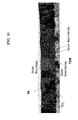
- FIG. 11 is an illustration showing an enlargement of the regions shown in FIG. 10 .
- FIG. 12 is an illustration representing the Fast Fourier Transforms and relative angular rotations of the regions R 1 to R 6 of the FIG. 11 .
- FIG. 14 is a selected area electron diffraction pattern of two (001)-oriented PZT grains separated by a low angle grain boundary resulting from a small angle rotation of one grain with respect to the other grain.
- FIG. 22 illustrates a schematic diagram of the growth of ⁇ 001 ⁇ -textured ferroelectric ⁇ PZT ⁇ .
- the PZT (PbZr 0.52 Ti 0.48 O 3 ; 52/48) may be deposited by metalorganic solution spin-on process, sputtering or metalorganic chemical vapor deposition (MOCVD).
- the PZT has a perovskite structure with ⁇ 001 ⁇ -texture.
- FIG. 23 graphically illustrates overlapping x-ray diffraction (XRD) ⁇ -2 ⁇ scans of as-deposited Mg films (deposited under various sputtering conditions) exhibiting only 0001 diffraction peaks and thus confirming the HCP structured Mg ⁇ 0001 ⁇ -texture.
- XRD x-ray diffraction
- FIG. 25 graphically illustrates an x-ray diffraction (XRD) ⁇ -2 ⁇ scan of an MgO film, formed by thermal oxidation of an Mg film heated in flowing oxygen at 625° C. for 30 min, exhibiting only 0001 diffraction peaks and thus confirming the rocksalt structure and MgO ⁇ 100 ⁇ -texture.
- XRD x-ray diffraction
- first, second, etc. may be used herein to describe various elements, components, regions, layers and/or sections, these elements, components, regions, layers and/or sections should not be limited by these terms. These terms are only used to distinguish one element, component, region, layer or section from another region, layer or section. Thus, a first element, component, region, layer or section discussed below could be termed a second element, component, region, layer or section without departing from the teachings of the present invention.
- relative terms such as “lower” or “bottom” and “upper” or “top,” may be used herein to describe one element's relationship to other elements as illustrated in the Figures. It will be understood that relative terms are intended to encompass different orientations of the device in addition to the orientation depicted in the Figures. For example, if the device in the Figures is turned over, elements described as being on the “lower” side of other elements would then be oriented on “upper” sides of the other elements. The exemplary term “lower”, can therefore, encompass both an orientation of “lower” and “upper,” depending of the particular orientation of the figure.
- the device in one of the figures is turned over, elements described as “below” or “beneath” other elements would then be oriented “above” the other elements.
- the exemplary terms “below” or “beneath” can, therefore, encompass both an orientation of above and below.
- the term “outer” may be used to refer to a surface and/or layer that is farthest away from a substrate.
- Embodiments of the present invention are described herein with reference to cross-section illustrations that are schematic illustrations of idealized embodiments of the present invention.
- the layers and/or regions illustrated in the figures are schematic in nature and their shapes are not intended to illustrate the precise shape of a region of a device and are not intended to limit the scope of the present invention.
- the layers are not drawn to relative scale.
- variations from the shapes are to be expected.
- embodiments of the present invention should not be construed as limited to the particular shapes of regions illustrated herein but are to include deviations in shapes.
- a region illustrated as a rectangle may have a variety of configurations without deviating from the present invention and/or may have tapered, rounded or curved features.
- references to a structure or feature that is disposed “adjacent” another feature may have portions that overlap or underlie the adjacent feature.
- Metal oxide single crystals exhibiting the rocksalt structure e.g. MgO, CaO, and NiO provide good epitaxial substrates for the growth of (100) Pt thin films when the substrate crystal is cut to provide a (100) substrate plane.
- ⁇ 100 ⁇ -textured MgO films can provide a seed layer for ⁇ 100 ⁇ -textured Pt thin films.
- a seed layer such as Fe, to initiate the textured growth of the MgO.
- PZT lead zirconate titanate
- Materials with these properties are used to create large force, large displacement actuators and sensors.
- PZT is one of the most economical ceramics that exhibits a high piezoelectric coefficient allowing for the use of lower voltages to achieve the same actuator performance metrics. It is highly desired to achieve highly ⁇ 001 ⁇ textured PZT (52/48). Proper control of the crystalline texture will allow an increase in the piezoelectric stress constant as shown by N. Ledermann, et. al.
- the piezoelectric coefficient of PZT is inherently linked to its crystalline quality and composition.
- the highest magnitude piezoelectric coefficients are observed at the PZT morphotropic phase boundary (MPB), where the crystal structure changes abruptly between the tetragonal and rhombohedral symmetry.
- MPB morphotropic phase boundary
- the MPB is located approximately at PbZr 0.52 Ti 0.48 O 3 , or PZT (52/48), composition.
- PZT thin films strongly influences the piezoelectric properties used in MEMS applications.
- PZT films are poled to saturation, the piezoelectric response increases sequentially on transforming from random orientation to ⁇ 111 ⁇ texture to ⁇ 001 ⁇ texture.
- Textured growth can be achieved by relying on crystal growth habit, but it can also be initiated by the use of a seed layer that provides a heteroepitaxial template.
- the choice of template and the process used to form it determines the structural quality and ultimately influences performance and reliability of MEMS PZT devices such as switches, filters, and actuators.
- PZT ⁇ 111 ⁇ -texture can be generated by taking advantage of a combination of crystal habit and templating mechanisms that occur in the PZT/bottom electrode stack.
- the process and material layer sequence may, for example, begin with ⁇ 0001 ⁇ -textured Ti ( FIGS. 2 and 3 deposited on PECVD or thermally grown SiO 2 on a Si wafer.
- the Ti is then converted to ⁇ 100 ⁇ -textured TiO 2 with the rutile structure ( FIG. 4 ) through thermal oxidation and then ⁇ 111 ⁇ -textured Pt ( FIGS. 5 and 6 ) can be grown on top of the ⁇ 100 ⁇ -textured TiO 2 .
- the ⁇ 111 ⁇ -textured Pt acts as a template for ⁇ 111 ⁇ -textured PZT ( FIG. 7 ) growth.
- the Ti and Pt are deposited by DC magnetron sputtering although other vapor deposition methods such as evaporation or metalorganic chemical vapor deposition can be used. Optimization of the TiO 2 and Pt film crystallographic textures and structures have been studied by variation of sputtering deposition times, temperatures and power levels, anneal conditions and substrate surface roughness. The correlations between the TiO 2 ⁇ 100 ⁇ -texture and the Pt ⁇ 111 ⁇ -texture and the Ti ⁇ 0001 ⁇ -texture and Pt ⁇ 111 ⁇ -texture qualities are illustrated by the results given in FIGS. 8 and 9 , respectively.
- ⁇ 111 ⁇ -textured PZT is produced when grown directly on ⁇ 111 ⁇ -textured Pt it is possible to induce the growth of ⁇ 001 ⁇ -textured PZT by placing seed layers at the PZT/Pt interface, Orientation control of lead zirconate titanate (PZT) thin films exhibiting a high degree of (001)-texture is desirable due to improved polarization and piezoelectric response.
- PZT lead zirconate titanate
- seed layers introduce composition gradients that cause a reduction in the magnitude of the ferroelectric spontaneous polarization, piezoelectric coefficients and reliability properties including polarization retention and cycling endurance.
- a seed layer such as PbTiO 3 (PT) is used on the surface of the bottom electrode, annealing conditions, PZT texture, composition, and optimization of the piezoelectric properties are interdependent and cannot be altered independently.
- the detrimental effects on the ferroelectric and piezoelectric properties of PZT due to the use of a PbTiO 3 seed layer can be minimized by employing a process resulting in a stylo-epitaxial structure. Formation of a stylo-epitaxial structure allows the ⁇ 001 ⁇ -texture of the PZT to be maximized, which is desirable, while it minimizes the composition gradients and electrode/PZT interface defects that detrimentally affect the device performance.
- PZT capacitor devices that exhibit stylo-epitaxy with those that do not exhibit stylo-epitaxy is provided in the following experimental results that use varying types of Pt electrodes.
- Ti/Pt and TiO 2 /Pt thins films were used as the base electrode for sol-gel PZT thin film growth (with silicon substrates and a 500 nm thermally grown silicon dioxide).
- the PZT may also be deposited by sputter deposition or MOCVD, but a spin-on chemical solution decomposition process was used for demonstrating the process herein.
- the Pt films were sputtered onto either the Ti metal film or a highly ⁇ 100 ⁇ -textured titanium dioxide film grown by a thermal oxidation process of a sputtered Ti film.
- Oriented (001)-texture in the PZT was obtained by using a seed layer of PbTiO 3 (PT) that was deposited on top of the Pt electrode.
- PbTiO 3 PbTiO 3
- the results indicate that the use of a highly oriented TiO 2 led to more highly (111)-textured Pt and improved PT and PZT orientations.
- PZT (52/48) and (45/55) thin films with and without PT seed layers were deposited and examined via x-ray diffraction methods (XRD) as a function of annealing temperature and the PbTiO 3 (PT) seed layer provided significant improvement in the (001) grain orientation while suppressing the (111) grain orientation of the PZT.
- XRD x-ray diffraction methods
- FIG. 10 Gowth of ⁇ 111 ⁇ -oriented Pt grains on ⁇ 100 ⁇ -oriented TiO 2 grains is observed in FIG. 10 .
- the lattice image FIG. 11 shows the alignment of the TiO 2 and Pt grain boundaries indicating grain-on-grain growth.
- Correlated rotations of the fast-fourier-transform images in FIG. 12 confirm alignment of the TiO 2 and Pt crystal structures of the corresponding grains marked in FIG. 11 .
- grain-grain-alignments of ⁇ 001 ⁇ -oriented PbTiO 3 grains on ⁇ 111 ⁇ -oriented Pt and ⁇ 001 ⁇ -oriented PZT on ⁇ 001 ⁇ -PbTiO 3 is shown in the TEM images of FIGS. 13 and 15 .
- Stylo-epitaxy of the TiO 2 /Pt/PT/PZT structure, where the Pt layer has a ⁇ 111 ⁇ -texture is confirmed by the combination of TEM, FFT, SAED and XRD results.
- a thermally oxidized ⁇ 100 ⁇ -textured seed layer such as MgO
- the Pt is grown with a ⁇ 100 ⁇ -texture that in-turn allows the growth of PZT and other perovskite structure thin films directly on the electrode with a ⁇ 100 ⁇ -texture and without the need for a PbTiO 3 seed layer. This allows some degree of independence of the PZT texture formation and the optimization of the PZT processing for composition and piezoelectric property control.
- stylo-epitaxy of the MgO/Pt/PZT stack is achieved resulting in ⁇ 001 ⁇ -textured PZT.
- the MgO/Mg system is self-seeding and relies on thermodynamically stable oxidation states and crystal habits when considering the growth conditions of the film.
- This processing method can be extended to any metal-oxide/metal seed layer system that can provide a good epitaxial match for the growth of Pt or related electrode materials.
- the approach can be applied to MgO, CaO, SrO, NiO, FeO, ScO, VO, CrO, CoO, MnO, CuO, SrO, NbO, PdO, CdO, BaO, SmO, and RaO etc.
- the technique of forming seed layers from textured metal films could also be used to achieve electrode crystallographic textures other than the ⁇ 100 ⁇ -texture.
- FIG. 16 illustrates a schematic diagram of textured metal deposition of a layer 3 on a layer or layers such as an SiO 2 layer 2 on an Si layer (or substrate) 1 .
- magnesium layer 3 B may be deposited by a DC magnetron sputtering in argon on layers 1 and 2 .
- FIG. 17 illustrates the atomic level packing within the textured grains where the magnesium atoms in the (0001)-plane, as viewed along the [0001]-direction, lie parallel to the substrate planar surface.
- FIG. 18 illustrates a schematic cross-section diagram of a ⁇ 100 ⁇ -textured oxide (1 nm to 1 ⁇ m thick, preferably 10 nm-100 nm thick) layer (layer 3 C) formed by thermal oxidation of the textured metal layer 3 A.
- the metal oxide layer, 3 C consists of the rocksalt crystal structure.
- the magnesium oxide layer 3 D may be formed by annealing the magnesium layer 3 B in flowing O 2 .
- the anneal temperature may be in the range from 100° C. to 650° C. and the first anneal may be followed by a second anneal in the temperature range between 500° C. and 1000° C. Oxidation of magnesium forms MgO with the rocksalt structure and ⁇ 100 ⁇ -texture.
- FIG. 19 is an atomic level illustration of the rocksalt structure, magnesium oxide, (100)-plane as viewed along the [100]-direction.
- FIG. 21 shows an atomic level illustration of how the atoms of a metal electrode in the (100)-plane and with the FCC crystal structure, in this case Pt, fit into the interstices of the (100)-plane of a rocksalt structure, metal oxide such as MgO. Both the Pt and MgO (100)-planes lie parallel to the surface of the substrate.
- FIG. 22 illustrates a cross-section schematic diagram of the growth of a ⁇ 001 ⁇ -textured perovskite ferroelectric layer 5 A.
- a ⁇ 001 ⁇ -textured ferroelectric layer PZT with a thickness of 10 nm to 10 ⁇ m may be deposited (layer 5 B).
- the PZT (PbZr 0.52 Ti 0.48 O 3 ) is deposited by a metalorganic solution spin-on process but may also be deposited by sputtering or MOCVD.
- the PZT has a perovskite structure with ⁇ 001 ⁇ -texture.
- the bottom electrode must exhibit a high density with a minimum of diffusion pathways (including pores and grain boundaries), and remain stable without degradation of the density and topography. If Pb depletion occurs at the ferroelectric/electrode interface, a low density electrode can allow Pb to diffuse completely through the Pt into the underlying SiO 2 layer. Pb reaction with SiO 2 causes both crystalline and amorphous lead silicate formation, compromising the electronic properties of the substrate and the PZT film.
- a powder diffractometer is utilized to obtain diffraction data for Ti, TiO 2 , Pt, Mg, and MgO thin films on SiO 2 coated Si substrates. Quantitative analysis of the diffraction data was used to determine the TiO 2 and Pt deposition conditions resulting in the highest level of Pt ⁇ 111 ⁇ -texture, which typically corresponds to optimal density and a minimized Pt and Pb diffusion during subsequent PZT processing. The objective of the Pt texture optimization study was to improve orientation, density and the interdependent electrical properties of the subsequently deposited PZT.
- Titanium films were sputter deposited on the as-received SiO 2 at a substrate temperature of 40° C. using a Unaxis Clusterline 200 chamber configured with a DC rotating-magnet magnetron and a 250 mm diameter, 99.99% pure Ti target.
- the deposited Ti thin films were converted to TiO 2 with an oxygen anneal in a Bruce Technologies InternationalTM 6 in. diameter quartz tube furnace. The furnace was heated, with 5 SLM flowing N 2 , to the setpoint (650° C.-800° C.).
- Characterization of the as-deposited metal films included multi-site, 4-point probe measurements of the sheet resistance and single-site X-ray diffraction (XRD) measurements, while characterization of the annealed TiO 2 films included multi-site ellipsometry measurements of thickness and refractive index and single-site XRD measurements.
- the sheet resistances, R s , of Ti and Pt films were measured on a Prometrics Versaprobe VP10 and a Four Dimensions, Model 280, Automatic Four-Point Probe Meter, respectively.
- Woollam ellipsometer model M-2000F was used for measuring the thickness, and refractive index of the as-received SiO 2 coatings and the annealed TiO 2 films, using a trial thickness of 500 nm (30 nm) for SiO 2 (TiO 2 ), Si and SiO 2 reference data, and TiO 2 Cauchy layer fitting parameters A n ⁇ 2.5 and B n ⁇ 0.05.
- a Rigaku Ultima III powder diffractometer with Bragg-Brentano optics, Cu X-ray source, graphite monochromator on the detector arm, and scintillation detector was used to make ⁇ -2 ⁇ and rocking-curve measurements on the thin film PZT, Pt, TiO 2 and Ti coated wafers.
- FIG. 2 shows a ⁇ -2 ⁇ XRD spectrum for a Ti thin film deposited at 0.5 kW, 30 sccm Ar, 24 s, and 40° C.
- the as-deposited Ti film had a nominal thickness of 21 nm and a measured sheet resistance of 89.9 Ohm/sq.
- FIG. 4 An example of a diffraction pattern for a TiO 2 film formed by thermal oxidation of the Ti film (annealed at 750° C. for 30 min) is shown in FIG. 4 .
- the TiO 2 film had a measured thickness of 32 nm and refractive index of 2.65.
- the diffraction pattern exhibits only rutile 200 and 400 peaks, indicative of a ⁇ 100 ⁇ -textured TiO 2 film.
- Variation in anneal temperature (650-800° C.) and anneal time (15-30 min) strongly affected the 200 and 400 TiO 2 diffraction peak positions, intensities, and widths but did not cause the appearance of any new diffraction peaks.
- the quantified parameters of the 200 and 400 TiO 2 peaks reached a plateau at 750-800° C. for 30 min anneal times, suggesting completion of the Ti-to-TiO 2 conversion under these conditions.
- FIG. 6 An illustration of the heteroepitaxial relationship between the Pt (111)-plane and the oxygen-terminated (100)-plane of rutile structure TiO 2 is shown in FIG. 6 .
- Direct observations of the Pt and TiO 2 grain-by-grain alignment are shown in FIGS. 10 and 11 and stylo-epitaxy is supported by the corresponding rotations of the FFT ( FIG. 12 ) from the contacting Pt and TiO 2 grains.
- Ti thin films in the range of 10-50 nm thickness can be deposited with a ⁇ 0001 ⁇ -textured HCP structure and converted to a ⁇ 100 ⁇ -textured TiO 2 with the rutile structure by using a thermal oxidation process.
- the ⁇ 100 ⁇ -textured TiO 2 can be used as a seed layer to grow a ⁇ 111 ⁇ -textured Pt via localized heteroepitaxy. Correlation of the 100 TiO 2 and 222 Pt rocking-curve FWHM was used to determine the heteroepitaxy seeding effect.
- the Pt electrode process change that results in improved ⁇ 111 ⁇ -textured Pt has resulted in the ⁇ 111 ⁇ -textured PZT growth.
- FIG. 24 graphically illustrates overlapping XRD rocking curves of the as-deposited Mg films of various thicknesses exhibiting only ⁇ 0001 ⁇ -texture with a tilt distribution width, RC-FWHM, of less than 15°.
- An illustration of the ideal atomic level HCP (0001) basal-plane of the Mg as viewed along the [0001]-direction is given in FIG. 17 . Broadening of the RC-FWHM results from increased tilting of Mg grains such that the (0001)-plane is not perfectly parallel with the planar substrate surface.
- FIG. 25 graphically illustrates an x-ray diffraction (XRD) ⁇ -2 ⁇ scan of an MgO film, formed by thermal oxidation of an Mg film heated in flowing oxygen at 625° C. for 30 min, The XRD of the MgO confirms the formation of the rocksalt structure and MgO ⁇ 100 ⁇ -texture.
- XRD x-ray diffraction
- metals such as Mg, Ca, Sr, Ni, Fe, Sc, V, Cr, Co, Mn, Cu, Sr, Nb, Pd, Cd, Ba, Sm, Ra and other metals exhibiting the HCP crystal structure can be sputter deposited to produce ⁇ 0001 ⁇ -texture films.
- the ⁇ 0001 ⁇ -textured metal films can then be thermally oxidized to produce the metal-oxide such as MgO, CaO, SrO, NiO, FeO, ScO, VO, CrO, CoO, MnO, CuO, SrO, NbO, PdO, CdO, BaO, SmO, and RaO with a rocksalt crystal structure.
- the ⁇ 0001 ⁇ -texture distribution of the metal is maintained such that the rocksalt structure, ⁇ 100 ⁇ -texture distribution of the metal-oxide film is similar.
- FIG. 21 illustrates, as an embodiment example, sputter-deposited platinum stylo-epitaxial layer and the registration of the Pt atoms in the (100)-plane with the interstices of the MgO rocksalt (100)-plane as viewed along the [100]-direction.
- Alternative electrode metals such as Ir, Au, Pd, Ru, Ag, Cu, Ni and other FCC structure metals can be seeded with MgO or related metal oxides to produce similarly ⁇ 100 ⁇ -textured electrodes.
- PZT can be grown with a ⁇ 001 ⁇ -texture.
- the metal films for the seed layer can be grown with a thermodynamically stable texture at low temperatures, e.g. ⁇ 600° C., using typical production, thin film, deposition tools.
- the texture of the metal thin film and subsequently formed oxide can be altered by changes in the metal thin-film deposition conditions. This will allow independent control of the texture of the subsequently deposited electrode and PZT films, altered or tuned by changes in the metal film processing.
- the oxidation process for converting the metal thin film to the oxide seed layer can be completely separated from the deposition process. The oxidation can be completed in a separate annealing tool instead of inside the metal deposition system. 6) Oxidation of the metal can be fully completed in order to obtain a thermodynamically stable film that is stable during subsequent electrode and PZT deposition. 7) The metal film could be incompletely oxidized or over-oxidized to tune the texture of the subsequent electrode and PZT layers.
- Preferred embodiments and/or principles of the present invention may be used in piezoelectric-MEMS devices such as micro-switches, resonators, micro-robotic actuators, micromotors and sensors. Additionally the invention can be used in ferroelectric random access memory (FRAM), resistive random access memories, photovoltaic devices, and biocompatible electrodes.
- FRAM ferroelectric random access memory
- Potential uses include, but are not limited to:
- Resistive memories that use conductive oxides, such as TiO 2 , NiO, etc.
- Electrodes for biological and medical applications Electrodes with different textures will likely have different activities and interactions with bio-molecules and structures.
- Indices used herein relate to Miller indices that are used in accordance with a crystallography notation system for planes and directions in crystal (Bravais) lattices.
- a family of lattice planes is determined by three integers h, k, and l (the Miller indices). They are written (hkl), and each index denotes a plane.
- negative integers are written with a bar, as in 3 for ⁇ 3.
- the integers are usually written in lowest terms, i.e. their greatest common divisor should be 1.
- the Miller index (100) represents a plane orthogonal to direction h; index (010) represents a plane orthogonal to direction k, and index (001) represents a plane orthogonal to l.
- the notation ⁇ hkl ⁇ denotes the set of all planes that are equivalent to (hkl) by the symmetry of the lattice.
- the corresponding notations are [hkl], with square instead of round brackets, denotes a direction in the basis of the direct lattice vectors instead of the reciprocal lattice; and similarly, the notation (hkl) denotes the set of all directions that are equivalent to [hkl] by symmetry.
- the terminology “register” in relation to a crystallographic structure means, with respect to two adjacent granular layers, the grains in a first granular layer are in registration with and contacting grains in the adjacent layer. For example, in an embodiment, each ferroelectric grain is in registration with one electrode grain.
- perovskite structure is any material with the same type of crystal structure as calcium titanium oxide (CaTiO 3 ), known as the perovskite structure, or XIIA2+VIB4+X2 ⁇ 3 with the oxygen in the face centers.
- the general chemical formula for perovskite compounds is ABX 3 , where ‘A’ and ‘B’ are two cations of very different sizes, and X is an anion that bonds to both.
- the ‘A’ atoms are larger than the ‘B’ atoms.
- the ideal cubic-symmetry structure has the B cation in 6-fold coordination, surrounded by an octahedron of anions, and the A cation in 12-fold cuboctahedral coordination.
- piezoelectric coefficient or Piezoelectric Modulus also known as d ij , for example d 33 , quantifies the volume change when a piezoelectic material is subject to an electric field, or the polarization on application of a stress:
- texture measurements refer to measurements used to determine the orientation distribution of crystalline grains in a polycrystalline sample.
- a material is termed textured if the grains are aligned in a preferred orientation along certain lattice planes.
- epitaxy refers to the deposition of a crystalline overlayer on a crystalline substrate, where the overlayer is in registry with the substrate at a preferred orientation of the overlayer with respect to the substrate for epitaxial growth.
- the overlayer is called an epitaxial film or epitaxial layer.
- Epitaxial deposition of a layer on a substrate matches the crystalline order of the substrate.
- growth plane refers to the epitaxial growth planes. Growth planes and their crystallographic axes may be expressed as, for example, [112] (111) X//[1100] (0001) Y, where X and Y are crystal materials and the (111) and (0001) are faces and the brackets [ ] indicate crystallographic axes.
- the perovskite crystal orientation having a ⁇ 001 ⁇ orientation means that the ⁇ 001 ⁇ planes of the perovskite crystal lie parallel to the growth plane.
- silo means, in combination with epitaxy, “column,” “pillar,” “tube,” or column-like crystal growth.
- columns or column-like structures refer to the column-like structures grown on top of granular regions.
- the column-like structures and granular regions are substantially coextensive.
- thin film is a layer of material ranging from fractions of a nanometer (monolayer) to several micrometers in thickness.
- rutile refers to a mineral composed primarily of the preferred polymorph of titanium dioxide, TiO 2 . Rutile is the most common natural form of TiO 2 .
- perovskite means is the crystal structure, as depicted in FIG. 1C , of any material with the same or substantially the same type of crystal structure as calcium titanium oxide (CaTiO 3 ), known as the perovskite structure.
- full width at half maximum is an expression of the extent of a function, given by the difference between the two extreme values of the independent variable at which the dependent variable is equal to half of its maximum value.
- crystallites refer to small, microscopic crystals that, held together through highly defective boundaries, constitute a polycrystalline solid. Crystallites are also referred to as grains.
- rocksalt or “sodium chloride” halite structure refers to a structure in which each of the two atom types forms a separate face-centered cubic lattice, with the two lattices interpenetrating.
Abstract
Description
5) The oxidation process for converting the metal thin film to the oxide seed layer can be completely separated from the deposition process. The oxidation can be completed in a separate annealing tool instead of inside the metal deposition system.
6) Oxidation of the metal can be fully completed in order to obtain a thermodynamically stable film that is stable during subsequent electrode and PZT deposition.
7) The metal film could be incompletely oxidized or over-oxidized to tune the texture of the subsequent electrode and PZT layers.
8) Gaseous species other than oxygen, such as N, F, Cl, C, could be incorporated in the oxidizing gas during the metal seed layer anneal in order to tune the seed layer texture and the texture of the subsequently deposited electrode and PZT layers.
Potential Uses
where P is polarization along the 3-direction, and σ is the stress along the 3-direction for the example d33. The i, j subscripts with the d coefficient refer to the reduced matrix notation for the piezoelectric coefficients of the third order piezoelectric tensor property
Claims (20)
Priority Applications (1)
| Application Number | Priority Date | Filing Date | Title |
|---|---|---|---|
| US13/488,925 US8866367B2 (en) | 2011-10-17 | 2012-06-05 | Thermally oxidized seed layers for the production of {001} textured electrodes and PZT devices and method of making |
Applications Claiming Priority (4)
| Application Number | Priority Date | Filing Date | Title |
|---|---|---|---|
| US201161547990P | 2011-10-17 | 2011-10-17 | |
| US201161547879P | 2011-10-17 | 2011-10-17 | |
| US13/436,349 US20130093290A1 (en) | 2011-10-17 | 2012-03-30 | Stylo-Epitaxial Piezoelectric and Ferroelectric Devices and Method of Manufacturing |
| US13/488,925 US8866367B2 (en) | 2011-10-17 | 2012-06-05 | Thermally oxidized seed layers for the production of {001} textured electrodes and PZT devices and method of making |
Related Parent Applications (1)
| Application Number | Title | Priority Date | Filing Date |
|---|---|---|---|
| US13/436,349 Continuation-In-Part US20130093290A1 (en) | 2011-10-17 | 2012-03-30 | Stylo-Epitaxial Piezoelectric and Ferroelectric Devices and Method of Manufacturing |
Publications (2)
| Publication Number | Publication Date |
|---|---|
| US20130093288A1 US20130093288A1 (en) | 2013-04-18 |
| US8866367B2 true US8866367B2 (en) | 2014-10-21 |
Family
ID=48085517
Family Applications (1)
| Application Number | Title | Priority Date | Filing Date |
|---|---|---|---|
| US13/488,925 Expired - Fee Related US8866367B2 (en) | 2011-10-17 | 2012-06-05 | Thermally oxidized seed layers for the production of {001} textured electrodes and PZT devices and method of making |
Country Status (1)
| Country | Link |
|---|---|
| US (1) | US8866367B2 (en) |
Cited By (5)
| Publication number | Priority date | Publication date | Assignee | Title |
|---|---|---|---|---|
| US20140217526A1 (en) * | 2013-01-08 | 2014-08-07 | T3Memory, Inc. | Novel perpendicular magnetoresistive elements |
| US10199063B2 (en) * | 2014-03-20 | 2019-02-05 | National Institute For Materials Science | Underlayer for perpendicularly magnetized film, perpendicularly magnetized film structure, perpendicular MTJ element, and perpendicular magnetic recording medium using the same |
| US10266936B2 (en) | 2011-10-17 | 2019-04-23 | The United States Of America As Represented By The Secretary Of The Army | Process for making lead zirconate titanate (PZT) layers and/or platinum electrodes and products thereof |
| US10854808B2 (en) * | 2014-10-23 | 2020-12-01 | Advanced Material Technologies, Inc. | Ferroelectric ceramics, electronic component and manufacturing method of ferroelectric ceramics |
| US11121139B2 (en) | 2017-11-16 | 2021-09-14 | International Business Machines Corporation | Hafnium oxide and zirconium oxide based ferroelectric devices with textured iridium bottom electrodes |
Families Citing this family (12)
| Publication number | Priority date | Publication date | Assignee | Title |
|---|---|---|---|---|
| US9203134B1 (en) * | 2013-02-28 | 2015-12-01 | Sandia Corporation | Tuning method for microresonators and microresonators made thereby |
| US10043565B2 (en) | 2014-03-14 | 2018-08-07 | The United States Of America As Represented By The Secretary Of The Army | Ferroelectric mechanical memory based on remanent displacement and method |
| US9722105B2 (en) * | 2014-03-28 | 2017-08-01 | Sunpower Corporation | Conversion of metal seed layer for buffer material |
| US20150380635A1 (en) * | 2014-06-30 | 2015-12-31 | Texas Instruments Incorporated | METHODS TO IMPROVE THE CRYSTALLINITY OF PbZrTiO3 AND Pt FILMS FOR MEMS APPLICATIONS |
| US9887344B2 (en) * | 2014-07-01 | 2018-02-06 | Seiko Epson Corporation | Piezoelectric element, piezoelectric actuator device, liquid ejecting head, liquid ejecting apparatus, and ultrasonic measuring apparatus |
| JP2016062984A (en) * | 2014-09-16 | 2016-04-25 | 株式会社リコー | Piezoelectric actuator and manufacturing method of the same, liquid cartridge, and image forming apparatus |
| US10160208B2 (en) * | 2016-04-11 | 2018-12-25 | Ricoh Company, Ltd. | Electromechanical-transducing electronic component, liquid discharge head, liquid discharge device, and liquid discharge apparatus |
| CN110088609A (en) | 2016-11-30 | 2019-08-02 | 美国圣戈班性能塑料公司 | Electrode and electrode manufacturing method |
| US10453913B2 (en) * | 2017-04-26 | 2019-10-22 | Samsung Electronics Co., Ltd. | Capacitor, semiconductor device and methods of manufacturing the capacitor and the semiconductor device |
| CN110514603B (en) * | 2019-09-24 | 2021-10-26 | 广西民族师范学院 | Photoelectrochemical sensor for detecting kanamycin and preparation method and application thereof |
| CN112555112B (en) * | 2020-11-06 | 2022-06-14 | 兰州空间技术物理研究所 | Textured special-shaped structure anode on inner surface of ion thruster based on 3D additive manufacturing |
| CN116682981A (en) * | 2023-07-31 | 2023-09-01 | 国家电投集团氢能科技发展有限公司 | Iridium-based anti-counter electrode catalyst and preparation method and application thereof |
Citations (94)
| Publication number | Priority date | Publication date | Assignee | Title |
|---|---|---|---|---|
| US4677336A (en) * | 1985-02-04 | 1987-06-30 | Hitachi, Ltd. | Piezoelectric transducer and process for its production |
| US5612536A (en) | 1994-02-07 | 1997-03-18 | Matsushita Electric Industrial Co., Ltd. | Thin film sensor element and method of manufacturing the same |
| US5662818A (en) | 1993-08-23 | 1997-09-02 | Matsushita Electric Industrial Co., Ltd. | Method of producing a pyroelectric infrared radiation detector |
| US5739563A (en) | 1995-03-15 | 1998-04-14 | Kabushiki Kaisha Toshiba | Ferroelectric type semiconductor device having a barium titanate type dielectric film and method for manufacturing the same |
| US5955213A (en) | 1995-08-25 | 1999-09-21 | Tdk Corporation | Ferroelectric thin film, electric device, and method for preparing ferroelectric thin film |
| US6054331A (en) | 1997-01-15 | 2000-04-25 | Tong Yang Cement Corporation | Apparatus and methods of depositing a platinum film with anti-oxidizing function over a substrate |
| US6312819B1 (en) * | 1999-05-26 | 2001-11-06 | The Regents Of The University Of California | Oriented conductive oxide electrodes on SiO2/Si and glass |
| US6319764B1 (en) | 1999-08-25 | 2001-11-20 | Micron Technology, Inc. | Method of forming haze-free BST films |
| US6347862B1 (en) | 1997-04-14 | 2002-02-19 | Matsushita Electric Industrial Co., Ltd. | Ink-jet head |
| US20030129307A1 (en) * | 2002-01-04 | 2003-07-10 | Rutgers, The State University Of New Jersey | Tailoring piezoelectric properties using MgxZn1-xO/ZnO material and MgxZn1-xO/ZnO structures |
| US6599757B1 (en) | 1998-10-14 | 2003-07-29 | Seiko Epson Corporation | Method for manufacturing ferroelectric thin film device, ink jet recording head, and ink jet printer |
| US6645807B2 (en) | 2001-09-06 | 2003-11-11 | Matsushita Electric Industrial Co., Ltd. | Method for manufacturing semiconductor device |
| US6682772B1 (en) | 2000-04-24 | 2004-01-27 | Ramtron International Corporation | High temperature deposition of Pt/TiOx for bottom electrodes |
| US6728093B2 (en) | 2002-07-03 | 2004-04-27 | Ramtron International Corporation | Method for producing crystallographically textured electrodes for textured PZT capacitors |
| US20040155559A1 (en) * | 2003-02-07 | 2004-08-12 | Canon Kabushiki Kaisha | Ferroelectric thin film element, piezoelectric actuator and liquid discharge head |
| US6822302B2 (en) | 2001-11-28 | 2004-11-23 | Seiko Epson Corporation | Substrate for electronic device, method for manufacturing substrate for electronic device, and electronic device |
| US6841817B2 (en) | 2001-11-01 | 2005-01-11 | Fujitsu Limited | Ferroelectric capacitor and a semiconductor device |
| US6853535B2 (en) | 2002-07-03 | 2005-02-08 | Ramtron International Corporation | Method for producing crystallographically textured electrodes for textured PZT capacitors |
| US6887716B2 (en) | 2000-12-20 | 2005-05-03 | Fujitsu Limited | Process for producing high quality PZT films for ferroelectric memory integrated circuits |
| US6889920B2 (en) | 2003-03-17 | 2005-05-10 | Westinghouse Savannah River Company | Directed spray mast |
| US6936837B2 (en) | 2001-05-11 | 2005-08-30 | Ube Industries, Ltd. | Film bulk acoustic resonator |
| US6943485B2 (en) | 2002-02-19 | 2005-09-13 | Seiko Epson Corporation | Piezoelectric actuator, liquid jetting head and liquid jetting device using the same |
| US6969157B2 (en) | 2002-05-31 | 2005-11-29 | Matsushita Electric Industrial Co., Ltd. | Piezoelectric element, ink jet head, angular velocity sensor, method for manufacturing the same, and ink jet recording apparatus |
| US7120978B2 (en) | 2000-06-21 | 2006-10-17 | Canon Kabushiki Kaisha | Process of manufacturing a piezoelectric element |
| US7153705B2 (en) | 2001-10-26 | 2006-12-26 | Fujitsu Limited | Electronic device with electrode and its manufacture |
| US7166954B2 (en) | 2003-11-05 | 2007-01-23 | Seiko Epson Corporation | Piezoelectric film, piezoelectric element, piezoelectric actuator, piezoelectric pump, ink-jet type recording head, ink-jet printer surface-acoustic-wave element, thin-film piezoelectric resonator, frequency filter, oscillator, electronic circuit, and electronic apparatus |
| US7185540B2 (en) | 2002-06-20 | 2007-03-06 | Matsushita Electric Industrial Co., Ltd. | Piezoelectric element, ink jet head, angular velocity sensor, method for manufacturing the same, and ink jet recording apparatus |
| US7193756B2 (en) | 2003-11-26 | 2007-03-20 | Matsushita Electric Industrial Co., Ltd. | Piezoelectric element, method for fabricating the same, inkjet head, method for fabricating the same, and inkjet recording apparatus |
| US7196457B2 (en) | 2003-10-23 | 2007-03-27 | Seiko Epson Corporation | Piezoelectric film, piezoelectric element, piezoelectric actuator, piezoelectric pump, ink-jet type recording head, ink-jet printer, surface-acoustic-wave element, thin-film piezoelectric resonator, frequency filter, oscillator, electronic circuit, and electronic apparatus |
| US7197799B2 (en) | 2003-12-02 | 2007-04-03 | Seiko Epson Corporation | Method for manufacturing a piezoelectric device |
| US7214977B2 (en) | 2002-12-27 | 2007-05-08 | Seiko Epson Corporation | Ferroelectric thin film, method of manufacturing the same, ferroelectric memory device and ferroelectric piezoelectric device |
| US7229662B2 (en) | 2003-12-16 | 2007-06-12 | National University Of Singapore | Heterolayered ferroelectric thin films and methods of forming same |
| US7240409B2 (en) | 1998-01-23 | 2007-07-10 | Seiko Epson Corporation | Process of making a piezoelectric thin film component |
| US7247975B2 (en) | 2004-03-29 | 2007-07-24 | Tdk Corporation | Thin-film piezoelectric element and method of making same |
| US7254877B2 (en) | 2001-02-09 | 2007-08-14 | Seiko Epson Corporation | Method for the manufacture of a piezoelectric element |
| US7262544B2 (en) | 2004-01-09 | 2007-08-28 | Canon Kabushiki Kaisha | Dielectric element, piezoelectric element, ink jet head and method for producing the same head |
| US7265483B2 (en) | 2004-03-29 | 2007-09-04 | Canon Kabushiki Kaisha | Dielectric member, piezoelectric member, ink jet head, ink jet recording apparatus and producing method for ink jet recording apparatus |
| US7268472B2 (en) | 2002-11-11 | 2007-09-11 | Seiko Epson Corporation | Piezoelectric device, liquid jetting head, ferroelectric device, electronic device and methods for manufacturing these devices |
| US7279825B2 (en) | 2003-12-10 | 2007-10-09 | Canon Kabushiki Kaisha | Dielectric thin film element, piezoelectric actuator and liquid discharge head, and method for manufacturing the same |
| US7279823B2 (en) | 2002-05-15 | 2007-10-09 | Seiko Epson Corporation | Piezoelectric actuator and liquid jet head |
| US7287840B2 (en) | 2004-05-17 | 2007-10-30 | Seiko Epson Corporation | Piezoelectric element, piezoelectric actuator, ink jet recording head, ink jet printer, surface acoustic wave element, frequency filter, oscillator, electronic circuit, thin film piezoelectric resonator and electronic apparatus |
| US7291960B2 (en) | 2004-12-28 | 2007-11-06 | Seiko Epson Corporation | Piezoelectric device, piezoelectric actuator, piezoelectric pump, inkjet recording head, inkjet printer, surface acoustic wave device, thin-film piezoelectric resonator, frequency filter, oscillator, electronic circuit, and electronic instrument |
| US7291959B2 (en) | 2004-05-17 | 2007-11-06 | Seiko Epson Corporation | Piezoelectric element, piezoelectric actuator, ink jet recording head, ink jet printer, surface acoustic wave element, frequency filter, oscillator, electronic circuit, thin film piezoelectric resonator and electronic apparatus |
| US7291520B2 (en) | 2002-06-24 | 2007-11-06 | Seiko Epson Corporation | Piezoelectric element and liquid jet head using the piezoelectric element |
| US7291530B2 (en) | 2003-06-10 | 2007-11-06 | Nec Electronics Corporation | Semiconductor storage device and method of manufacturing the same |
| US7298018B2 (en) | 2004-12-02 | 2007-11-20 | Agency For Science, Technology And Research | PLT/PZT ferroelectric structure |
| US7303828B2 (en) | 2003-03-28 | 2007-12-04 | Seiko Epson Corporation | Ferroelectric film, method of manufacturing the same, ferroelectric memory and piezoelectric device |
| US7309950B1 (en) | 2005-08-23 | 2007-12-18 | Canon Kabushiki Kaisha | Piezoelectric device, liquid discharge head employing this device and liquid discharge apparatus |
| US7312558B2 (en) | 2004-04-02 | 2007-12-25 | Matsushita Electric Industrial Co., Ltd. | Piezoelectric element, ink jet head, angular velocity sensor, and ink jet recording apparatus |
| US7310862B2 (en) | 2003-12-01 | 2007-12-25 | Seiko Epson Corporation | Method for manufacturing a piezoelectric device |
| US7320163B2 (en) | 2004-03-11 | 2008-01-22 | Seiko Epson Corporation | Method of manufacturing an actuator device |
| US7328490B2 (en) | 2002-01-22 | 2008-02-12 | Seiko Epson Corporation | Method for manufacturing a liquid jetting head |
| US7339219B2 (en) | 2003-03-04 | 2008-03-04 | Fujitsu Limited | Capacitance device including a perovskite film having (001) orientation |
| US7343654B2 (en) | 2004-01-23 | 2008-03-18 | Seiko Epson Corporation | Method of manufacturing a piezoelectric element and a liquid ink jet head |
| US7348715B2 (en) | 2004-01-27 | 2008-03-25 | Matsushita Electric Industrial Co., Ltd. | Piezoelectric element and method for manufacturing the same, and ink jet head and ink jet recording apparatus using the piezoelectric element |
| US7350904B2 (en) | 2004-01-26 | 2008-04-01 | Seiko Epson Corporation | Piezoelectric element, piezoelectric actuator, ink jet recording head, ink jet printer, surface acoustic wave element, frequency filter, oscillator, electronic circuit, thin film piezoelectric resonator, and electronic apparatus |
| US20080083452A1 (en) * | 2004-05-14 | 2008-04-10 | Sony Corporation | Photoelectric Converter, and Transparent Conductive Substrate for the same |
| US7368172B2 (en) | 2003-06-11 | 2008-05-06 | Fujitsu Limited | Membrane multi-layer structure, and actuator element, capacitive element and filter element using the same |
| US7427515B2 (en) | 2004-03-31 | 2008-09-23 | Fujitsu Limited | Electronic element including ferroelectric substance film and method of manufacturing the same |
| US7446361B2 (en) | 2002-12-10 | 2008-11-04 | Fujitsu Limited | Capacitor and semiconductor device having a ferroelectric material |
| US7478558B2 (en) | 2001-12-18 | 2009-01-20 | Panasonic Corporation | Piezoelectric element, ink jet head, angular velocity sensor, method for manufacturing the same, and ink jet recording apparatus |
| US7513608B2 (en) | 2003-02-07 | 2009-04-07 | Canon Kabushiki Kaisha | Dielectric film structure, piezoelectric actuator using dielectric element film structure and ink jet head |
| US7521845B2 (en) | 2005-08-23 | 2009-04-21 | Canon Kabushiki Kaisha | Piezoelectric substance, piezoelectric element, liquid discharge head using piezoelectric element, and liquid discharge apparatus |
| US7535157B2 (en) | 2006-09-08 | 2009-05-19 | Seiko Epson Corporation | Piezoelectric element, actuator device, liquid-jet head, and liquid-jet apparatus |
| US7547933B2 (en) | 2002-10-30 | 2009-06-16 | Fujitsu Microelectronics Limited | Semiconductor device and manufacturing method of a semiconductor device |
| US7562968B2 (en) | 2005-03-30 | 2009-07-21 | Seiko Epson Corporation | Piezoelectric element, liquid-jet head and liquid-jet apparatus |
| US7568792B2 (en) | 2005-03-28 | 2009-08-04 | Seiko Epson Corporation | Piezoelectric element, actuator device, liquid-jet head and liquid-jet apparatus |
| US7579041B2 (en) | 2003-12-11 | 2009-08-25 | Seiko Epson Corporation | Method of manufacturing dielectric layer and method of manufacturing liquid jet head |
| US7589450B2 (en) | 2005-07-08 | 2009-09-15 | Seiko Epson Corporation | Actuator device, liquid-jet head and liquid-jet apparatus |
| US7608981B2 (en) | 2005-06-15 | 2009-10-27 | Tdk Corporation | Piezoelectric thin film vibrator and fabrication method thereof, driving apparatus and piezoelectric motor using the same |
| US7614128B2 (en) | 2005-07-05 | 2009-11-10 | Seiko Epson Corporation | Method of manufacturing piezoelectric element and method of manufacturing liquid-jet head |
| US7622852B2 (en) | 2007-03-02 | 2009-11-24 | Canon Kabushiki Kaisha | Piezoelectric member, piezoelectric element, and liquid discharge head and liquid discharge apparatus utilizing piezoelectric element |
| US7622850B2 (en) | 2004-12-28 | 2009-11-24 | Seiko Epson Corporation | Piezoelectric device, piezoelectric actuator, piezoelectric pump, inkjet recording head, inkjet printer, surface acoustic wave device, thin-film piezoelectric resonator, frequency filter, oscillator, electronic circuit, and electronic instrument |
| US7646073B2 (en) | 2006-03-08 | 2010-01-12 | Seiko Epson Corporation | Ferroelectric capacitor and ferroelectric memory |
| US20100006780A1 (en) | 2008-05-06 | 2010-01-14 | U.S. Government As Represented By The Secretary Of The Army | Method and Apparatus for Enhanced Terahertz Radiation from High Stacking Fault Density |
| US7652408B2 (en) * | 2006-04-07 | 2010-01-26 | Fujifilm Corporation | Piezoelectric devices, process for producing the piezoelectric device, and inkjet recording head |
| US7651199B2 (en) | 2005-03-28 | 2010-01-26 | Seiko Epson Corporation | Piezoelectric element, actuator device, liquid-jet head and liquid-jet apparatus |
| US7708289B2 (en) | 2007-09-07 | 2010-05-04 | Jaime Sr Richard A | Removable tubular variable lighting system for a skateboard |
| US7712878B2 (en) | 2007-03-29 | 2010-05-11 | Seiko Epson Corporation | Liquid ejecting head and method for manufacturing the same |
| US7717546B2 (en) | 2006-07-19 | 2010-05-18 | Seiko Epson Corporation | Piezoelectric device and liquid jet head |
| US7725996B2 (en) | 2005-08-09 | 2010-06-01 | Seiko Epson Corporation | Method for producing actuator device |
| US7768178B2 (en) | 2007-07-27 | 2010-08-03 | Fujifilm Corporation | Piezoelectric device, piezoelectric actuator, and liquid discharge device having piezoelectric films |
| US7768050B2 (en) | 2006-07-07 | 2010-08-03 | The Trustees Of The University Of Pennsylvania | Ferroelectric thin films |
| US7786964B2 (en) | 2005-04-04 | 2010-08-31 | Canon Kabushiki Kaisha | Display apparatus and display control method therefor |
| US7786656B2 (en) | 2007-04-26 | 2010-08-31 | Fujifilm Corporation | Piezoelectric body, piezoelectric device, and liquid discharge apparatus |
| US7785659B2 (en) | 2005-03-22 | 2010-08-31 | Fujifilm Corporation | Method of manufacturing an orientation film using aerosol deposition on a seed substrate |
| US7804231B2 (en) | 2005-09-05 | 2010-09-28 | Canon Kabushiki Kaisha | Epitaxial oxide film, piezoelectric film, piezoelectric film element, liquid discharge head using the piezoelectric film element, and liquid discharge apparatus |
| US7810915B2 (en) | 2006-04-03 | 2010-10-12 | Seiko Epson Corporation | Actuator device, liquid-jet head and liquid-jet apparatus |
| US7816842B2 (en) | 2007-03-26 | 2010-10-19 | Fujifilm Corporation | Patterned inorganic film formed of an inorganic material on a metal film having a surface which includes a plurality of surface-oxidized areas, piezoelectric device having the patterned inorganic film, and process for producing the inorganic film |
| US7819508B2 (en) | 2005-03-31 | 2010-10-26 | Seiko Epson Corporation | Dielectric film and piezoelectric element |
| US7827658B2 (en) | 2006-03-28 | 2010-11-09 | Seiko Epson Corporation | Method for manufacturing actuator device and liquid ejecting head including actuator device prepared by the method |
| US7830073B2 (en) | 2006-05-25 | 2010-11-09 | Fujifilm Corporation | Perovskite oxide, electric element, piezoelectric actuator and liquid discharge system |
| US7837305B2 (en) | 2007-01-30 | 2010-11-23 | Panasonic Corporation | Piezoelectric element, ink jet head, and ink jet recording device |
| US7956369B2 (en) | 2008-05-07 | 2011-06-07 | The United States Of America As Represented By The Secretary Of The Army | Light emitting diode |
-
2012
- 2012-06-05 US US13/488,925 patent/US8866367B2/en not_active Expired - Fee Related
Patent Citations (99)
| Publication number | Priority date | Publication date | Assignee | Title |
|---|---|---|---|---|
| US4677336A (en) * | 1985-02-04 | 1987-06-30 | Hitachi, Ltd. | Piezoelectric transducer and process for its production |
| US5662818A (en) | 1993-08-23 | 1997-09-02 | Matsushita Electric Industrial Co., Ltd. | Method of producing a pyroelectric infrared radiation detector |
| US5612536A (en) | 1994-02-07 | 1997-03-18 | Matsushita Electric Industrial Co., Ltd. | Thin film sensor element and method of manufacturing the same |
| US6105225A (en) | 1994-02-07 | 2000-08-22 | Matsushita Electric Industrial Co., Ltd. | Method of manufacturing a thin film sensor element |
| US5739563A (en) | 1995-03-15 | 1998-04-14 | Kabushiki Kaisha Toshiba | Ferroelectric type semiconductor device having a barium titanate type dielectric film and method for manufacturing the same |
| US5955213A (en) | 1995-08-25 | 1999-09-21 | Tdk Corporation | Ferroelectric thin film, electric device, and method for preparing ferroelectric thin film |
| US6054331A (en) | 1997-01-15 | 2000-04-25 | Tong Yang Cement Corporation | Apparatus and methods of depositing a platinum film with anti-oxidizing function over a substrate |
| US6347862B1 (en) | 1997-04-14 | 2002-02-19 | Matsushita Electric Industrial Co., Ltd. | Ink-jet head |
| US7240409B2 (en) | 1998-01-23 | 2007-07-10 | Seiko Epson Corporation | Process of making a piezoelectric thin film component |
| US6599757B1 (en) | 1998-10-14 | 2003-07-29 | Seiko Epson Corporation | Method for manufacturing ferroelectric thin film device, ink jet recording head, and ink jet printer |
| US6312819B1 (en) * | 1999-05-26 | 2001-11-06 | The Regents Of The University Of California | Oriented conductive oxide electrodes on SiO2/Si and glass |
| US6319764B1 (en) | 1999-08-25 | 2001-11-20 | Micron Technology, Inc. | Method of forming haze-free BST films |
| US6682772B1 (en) | 2000-04-24 | 2004-01-27 | Ramtron International Corporation | High temperature deposition of Pt/TiOx for bottom electrodes |
| US7120978B2 (en) | 2000-06-21 | 2006-10-17 | Canon Kabushiki Kaisha | Process of manufacturing a piezoelectric element |
| US7618131B2 (en) | 2000-06-21 | 2009-11-17 | Canon Kabushiki Kaisha | Structure of piezoelectric element and liquid discharge recording head, and method of manufacture therefor |
| US6887716B2 (en) | 2000-12-20 | 2005-05-03 | Fujitsu Limited | Process for producing high quality PZT films for ferroelectric memory integrated circuits |
| US7254877B2 (en) | 2001-02-09 | 2007-08-14 | Seiko Epson Corporation | Method for the manufacture of a piezoelectric element |
| US6936837B2 (en) | 2001-05-11 | 2005-08-30 | Ube Industries, Ltd. | Film bulk acoustic resonator |
| US6645807B2 (en) | 2001-09-06 | 2003-11-11 | Matsushita Electric Industrial Co., Ltd. | Method for manufacturing semiconductor device |
| US7153705B2 (en) | 2001-10-26 | 2006-12-26 | Fujitsu Limited | Electronic device with electrode and its manufacture |
| US6841817B2 (en) | 2001-11-01 | 2005-01-11 | Fujitsu Limited | Ferroelectric capacitor and a semiconductor device |
| US7423308B2 (en) | 2001-11-01 | 2008-09-09 | Fujitsu Limited | Ferroelectric capacitor |
| US6822302B2 (en) | 2001-11-28 | 2004-11-23 | Seiko Epson Corporation | Substrate for electronic device, method for manufacturing substrate for electronic device, and electronic device |
| US7247551B2 (en) | 2001-11-28 | 2007-07-24 | Seiko Epson Corporation | Substrate for electronic device, method for manufacturing substrate for electronic device, and electronic device |
| US7478558B2 (en) | 2001-12-18 | 2009-01-20 | Panasonic Corporation | Piezoelectric element, ink jet head, angular velocity sensor, method for manufacturing the same, and ink jet recording apparatus |
| US20030129307A1 (en) * | 2002-01-04 | 2003-07-10 | Rutgers, The State University Of New Jersey | Tailoring piezoelectric properties using MgxZn1-xO/ZnO material and MgxZn1-xO/ZnO structures |
| US7328490B2 (en) | 2002-01-22 | 2008-02-12 | Seiko Epson Corporation | Method for manufacturing a liquid jetting head |
| US6943485B2 (en) | 2002-02-19 | 2005-09-13 | Seiko Epson Corporation | Piezoelectric actuator, liquid jetting head and liquid jetting device using the same |
| US7279823B2 (en) | 2002-05-15 | 2007-10-09 | Seiko Epson Corporation | Piezoelectric actuator and liquid jet head |
| US6969157B2 (en) | 2002-05-31 | 2005-11-29 | Matsushita Electric Industrial Co., Ltd. | Piezoelectric element, ink jet head, angular velocity sensor, method for manufacturing the same, and ink jet recording apparatus |
| US7185540B2 (en) | 2002-06-20 | 2007-03-06 | Matsushita Electric Industrial Co., Ltd. | Piezoelectric element, ink jet head, angular velocity sensor, method for manufacturing the same, and ink jet recording apparatus |
| US7291520B2 (en) | 2002-06-24 | 2007-11-06 | Seiko Epson Corporation | Piezoelectric element and liquid jet head using the piezoelectric element |
| US6728093B2 (en) | 2002-07-03 | 2004-04-27 | Ramtron International Corporation | Method for producing crystallographically textured electrodes for textured PZT capacitors |
| US6853535B2 (en) | 2002-07-03 | 2005-02-08 | Ramtron International Corporation | Method for producing crystallographically textured electrodes for textured PZT capacitors |
| US7547933B2 (en) | 2002-10-30 | 2009-06-16 | Fujitsu Microelectronics Limited | Semiconductor device and manufacturing method of a semiconductor device |
| US7268472B2 (en) | 2002-11-11 | 2007-09-11 | Seiko Epson Corporation | Piezoelectric device, liquid jetting head, ferroelectric device, electronic device and methods for manufacturing these devices |
| US7446361B2 (en) | 2002-12-10 | 2008-11-04 | Fujitsu Limited | Capacitor and semiconductor device having a ferroelectric material |
| US7214977B2 (en) | 2002-12-27 | 2007-05-08 | Seiko Epson Corporation | Ferroelectric thin film, method of manufacturing the same, ferroelectric memory device and ferroelectric piezoelectric device |
| US7215067B2 (en) | 2003-02-07 | 2007-05-08 | Canon Kabushiki Kaisha | Ferroelectric thin film element, piezoelectric actuator and liquid discharge head |
| US20040155559A1 (en) * | 2003-02-07 | 2004-08-12 | Canon Kabushiki Kaisha | Ferroelectric thin film element, piezoelectric actuator and liquid discharge head |
| US7513608B2 (en) | 2003-02-07 | 2009-04-07 | Canon Kabushiki Kaisha | Dielectric film structure, piezoelectric actuator using dielectric element film structure and ink jet head |
| US7339219B2 (en) | 2003-03-04 | 2008-03-04 | Fujitsu Limited | Capacitance device including a perovskite film having (001) orientation |
| US6889920B2 (en) | 2003-03-17 | 2005-05-10 | Westinghouse Savannah River Company | Directed spray mast |
| US7303828B2 (en) | 2003-03-28 | 2007-12-04 | Seiko Epson Corporation | Ferroelectric film, method of manufacturing the same, ferroelectric memory and piezoelectric device |
| US7291530B2 (en) | 2003-06-10 | 2007-11-06 | Nec Electronics Corporation | Semiconductor storage device and method of manufacturing the same |
| US7368172B2 (en) | 2003-06-11 | 2008-05-06 | Fujitsu Limited | Membrane multi-layer structure, and actuator element, capacitive element and filter element using the same |
| US7196457B2 (en) | 2003-10-23 | 2007-03-27 | Seiko Epson Corporation | Piezoelectric film, piezoelectric element, piezoelectric actuator, piezoelectric pump, ink-jet type recording head, ink-jet printer, surface-acoustic-wave element, thin-film piezoelectric resonator, frequency filter, oscillator, electronic circuit, and electronic apparatus |
| US7166954B2 (en) | 2003-11-05 | 2007-01-23 | Seiko Epson Corporation | Piezoelectric film, piezoelectric element, piezoelectric actuator, piezoelectric pump, ink-jet type recording head, ink-jet printer surface-acoustic-wave element, thin-film piezoelectric resonator, frequency filter, oscillator, electronic circuit, and electronic apparatus |
| US7193756B2 (en) | 2003-11-26 | 2007-03-20 | Matsushita Electric Industrial Co., Ltd. | Piezoelectric element, method for fabricating the same, inkjet head, method for fabricating the same, and inkjet recording apparatus |
| US7310862B2 (en) | 2003-12-01 | 2007-12-25 | Seiko Epson Corporation | Method for manufacturing a piezoelectric device |
| US7197799B2 (en) | 2003-12-02 | 2007-04-03 | Seiko Epson Corporation | Method for manufacturing a piezoelectric device |
| US7279825B2 (en) | 2003-12-10 | 2007-10-09 | Canon Kabushiki Kaisha | Dielectric thin film element, piezoelectric actuator and liquid discharge head, and method for manufacturing the same |
| US7579041B2 (en) | 2003-12-11 | 2009-08-25 | Seiko Epson Corporation | Method of manufacturing dielectric layer and method of manufacturing liquid jet head |
| US7229662B2 (en) | 2003-12-16 | 2007-06-12 | National University Of Singapore | Heterolayered ferroelectric thin films and methods of forming same |
| US7262544B2 (en) | 2004-01-09 | 2007-08-28 | Canon Kabushiki Kaisha | Dielectric element, piezoelectric element, ink jet head and method for producing the same head |
| US7343654B2 (en) | 2004-01-23 | 2008-03-18 | Seiko Epson Corporation | Method of manufacturing a piezoelectric element and a liquid ink jet head |
| US7350904B2 (en) | 2004-01-26 | 2008-04-01 | Seiko Epson Corporation | Piezoelectric element, piezoelectric actuator, ink jet recording head, ink jet printer, surface acoustic wave element, frequency filter, oscillator, electronic circuit, thin film piezoelectric resonator, and electronic apparatus |
| US7348715B2 (en) | 2004-01-27 | 2008-03-25 | Matsushita Electric Industrial Co., Ltd. | Piezoelectric element and method for manufacturing the same, and ink jet head and ink jet recording apparatus using the piezoelectric element |
| US7320163B2 (en) | 2004-03-11 | 2008-01-22 | Seiko Epson Corporation | Method of manufacturing an actuator device |
| US7265483B2 (en) | 2004-03-29 | 2007-09-04 | Canon Kabushiki Kaisha | Dielectric member, piezoelectric member, ink jet head, ink jet recording apparatus and producing method for ink jet recording apparatus |
| US7247975B2 (en) | 2004-03-29 | 2007-07-24 | Tdk Corporation | Thin-film piezoelectric element and method of making same |
| US7427515B2 (en) | 2004-03-31 | 2008-09-23 | Fujitsu Limited | Electronic element including ferroelectric substance film and method of manufacturing the same |
| US7312558B2 (en) | 2004-04-02 | 2007-12-25 | Matsushita Electric Industrial Co., Ltd. | Piezoelectric element, ink jet head, angular velocity sensor, and ink jet recording apparatus |
| US20080083452A1 (en) * | 2004-05-14 | 2008-04-10 | Sony Corporation | Photoelectric Converter, and Transparent Conductive Substrate for the same |
| US7291959B2 (en) | 2004-05-17 | 2007-11-06 | Seiko Epson Corporation | Piezoelectric element, piezoelectric actuator, ink jet recording head, ink jet printer, surface acoustic wave element, frequency filter, oscillator, electronic circuit, thin film piezoelectric resonator and electronic apparatus |
| US7287840B2 (en) | 2004-05-17 | 2007-10-30 | Seiko Epson Corporation | Piezoelectric element, piezoelectric actuator, ink jet recording head, ink jet printer, surface acoustic wave element, frequency filter, oscillator, electronic circuit, thin film piezoelectric resonator and electronic apparatus |
| US7298018B2 (en) | 2004-12-02 | 2007-11-20 | Agency For Science, Technology And Research | PLT/PZT ferroelectric structure |
| US7622850B2 (en) | 2004-12-28 | 2009-11-24 | Seiko Epson Corporation | Piezoelectric device, piezoelectric actuator, piezoelectric pump, inkjet recording head, inkjet printer, surface acoustic wave device, thin-film piezoelectric resonator, frequency filter, oscillator, electronic circuit, and electronic instrument |
| US7291960B2 (en) | 2004-12-28 | 2007-11-06 | Seiko Epson Corporation | Piezoelectric device, piezoelectric actuator, piezoelectric pump, inkjet recording head, inkjet printer, surface acoustic wave device, thin-film piezoelectric resonator, frequency filter, oscillator, electronic circuit, and electronic instrument |
| US7785659B2 (en) | 2005-03-22 | 2010-08-31 | Fujifilm Corporation | Method of manufacturing an orientation film using aerosol deposition on a seed substrate |
| US7568792B2 (en) | 2005-03-28 | 2009-08-04 | Seiko Epson Corporation | Piezoelectric element, actuator device, liquid-jet head and liquid-jet apparatus |
| US7651199B2 (en) | 2005-03-28 | 2010-01-26 | Seiko Epson Corporation | Piezoelectric element, actuator device, liquid-jet head and liquid-jet apparatus |
| US7562968B2 (en) | 2005-03-30 | 2009-07-21 | Seiko Epson Corporation | Piezoelectric element, liquid-jet head and liquid-jet apparatus |
| US7819508B2 (en) | 2005-03-31 | 2010-10-26 | Seiko Epson Corporation | Dielectric film and piezoelectric element |
| US7786964B2 (en) | 2005-04-04 | 2010-08-31 | Canon Kabushiki Kaisha | Display apparatus and display control method therefor |
| US7608981B2 (en) | 2005-06-15 | 2009-10-27 | Tdk Corporation | Piezoelectric thin film vibrator and fabrication method thereof, driving apparatus and piezoelectric motor using the same |
| US7614128B2 (en) | 2005-07-05 | 2009-11-10 | Seiko Epson Corporation | Method of manufacturing piezoelectric element and method of manufacturing liquid-jet head |
| US7589450B2 (en) | 2005-07-08 | 2009-09-15 | Seiko Epson Corporation | Actuator device, liquid-jet head and liquid-jet apparatus |
| US7725996B2 (en) | 2005-08-09 | 2010-06-01 | Seiko Epson Corporation | Method for producing actuator device |
| US7521845B2 (en) | 2005-08-23 | 2009-04-21 | Canon Kabushiki Kaisha | Piezoelectric substance, piezoelectric element, liquid discharge head using piezoelectric element, and liquid discharge apparatus |
| US7309950B1 (en) | 2005-08-23 | 2007-12-18 | Canon Kabushiki Kaisha | Piezoelectric device, liquid discharge head employing this device and liquid discharge apparatus |
| US7804231B2 (en) | 2005-09-05 | 2010-09-28 | Canon Kabushiki Kaisha | Epitaxial oxide film, piezoelectric film, piezoelectric film element, liquid discharge head using the piezoelectric film element, and liquid discharge apparatus |
| US7646073B2 (en) | 2006-03-08 | 2010-01-12 | Seiko Epson Corporation | Ferroelectric capacitor and ferroelectric memory |
| US7827658B2 (en) | 2006-03-28 | 2010-11-09 | Seiko Epson Corporation | Method for manufacturing actuator device and liquid ejecting head including actuator device prepared by the method |
| US7810915B2 (en) | 2006-04-03 | 2010-10-12 | Seiko Epson Corporation | Actuator device, liquid-jet head and liquid-jet apparatus |
| US7652408B2 (en) * | 2006-04-07 | 2010-01-26 | Fujifilm Corporation | Piezoelectric devices, process for producing the piezoelectric device, and inkjet recording head |
| US7830073B2 (en) | 2006-05-25 | 2010-11-09 | Fujifilm Corporation | Perovskite oxide, electric element, piezoelectric actuator and liquid discharge system |
| US7768050B2 (en) | 2006-07-07 | 2010-08-03 | The Trustees Of The University Of Pennsylvania | Ferroelectric thin films |
| US7717546B2 (en) | 2006-07-19 | 2010-05-18 | Seiko Epson Corporation | Piezoelectric device and liquid jet head |
| US7535157B2 (en) | 2006-09-08 | 2009-05-19 | Seiko Epson Corporation | Piezoelectric element, actuator device, liquid-jet head, and liquid-jet apparatus |
| US7837305B2 (en) | 2007-01-30 | 2010-11-23 | Panasonic Corporation | Piezoelectric element, ink jet head, and ink jet recording device |
| US7622852B2 (en) | 2007-03-02 | 2009-11-24 | Canon Kabushiki Kaisha | Piezoelectric member, piezoelectric element, and liquid discharge head and liquid discharge apparatus utilizing piezoelectric element |
| US7816842B2 (en) | 2007-03-26 | 2010-10-19 | Fujifilm Corporation | Patterned inorganic film formed of an inorganic material on a metal film having a surface which includes a plurality of surface-oxidized areas, piezoelectric device having the patterned inorganic film, and process for producing the inorganic film |
| US7712878B2 (en) | 2007-03-29 | 2010-05-11 | Seiko Epson Corporation | Liquid ejecting head and method for manufacturing the same |
| US7786656B2 (en) | 2007-04-26 | 2010-08-31 | Fujifilm Corporation | Piezoelectric body, piezoelectric device, and liquid discharge apparatus |
| US7768178B2 (en) | 2007-07-27 | 2010-08-03 | Fujifilm Corporation | Piezoelectric device, piezoelectric actuator, and liquid discharge device having piezoelectric films |
| US7708289B2 (en) | 2007-09-07 | 2010-05-04 | Jaime Sr Richard A | Removable tubular variable lighting system for a skateboard |
| US20100006780A1 (en) | 2008-05-06 | 2010-01-14 | U.S. Government As Represented By The Secretary Of The Army | Method and Apparatus for Enhanced Terahertz Radiation from High Stacking Fault Density |
| US7956369B2 (en) | 2008-05-07 | 2011-06-07 | The United States Of America As Represented By The Secretary Of The Army | Light emitting diode |
Non-Patent Citations (23)
| Title |
|---|
| Dubois, et al , "Which PZT Thin Films for Piezoelectric Microactuator Applications?" Integrated Ferroelectrics vol. 22 . pp. 535 543 (1998). |
| F. Tyholdt, et al. "Chemically derived seeding layer for {100}-textured PZT thin films," J Electroceram (2007) 19:311-314 DOI 10.1007/s10832-007-9037-2. |
| F.K. Lofgering, "Topotactical reactions with ferrimagnetic oxides having hexagonal crystal structures-l" Philips Research Laboratories, N. V. Philips' Gloeilampenfabrieken, Eindhoven, Netherlands, Journal of Inorganic and Nuclear Chemistry vol. 9, Issue 2, Feb. 1959, pp. 113-123. |
| Hiboux, H., et al. "Mixed titania-lead oxide seed layers for PZT growth on Pt(111):a study on nucleation, texture and properties," Journal of the European Ceramic Society 24 (2004) 1593-1596. |
| Hiboux, S, et al., "Orientation and Composition Dependence of Piezoelectric Dielecfric Properties of Sputiered Pb(Zr x,Ti (1-x))O3 Thin Films," Materials Research Society, Met. Res. Sec. Symp. Proc. (2000) p. 499. |
| Hiratani, M., "Ultra-thin Titanium oxide Film with a Rutile-type structure," Appl. Surf. Science 207, pp. 13-19 (2003). |
| M.D. Vaudin, et el., "Accuracy and Reproducibility of X-ray Texture Measurements on Thin Films," Mat. Res. Soc. Symp. Proc, vol. 721, entitled "Magnetic and Electronic Films-Microstructure, Texture and Application to Data Storage," edited by P.W. DeHaven et al. (Mat Res. Soc., Warrendale PA, 2002) pp. 17-22. |
| Maeder, T., "Thin Films by In-situ Reactive Sputtering on Micromachined Membranes for Micromehanical Applications," British Ceramic Proceedings, lssue 54, 1996, pp. 206-218. |
| Matsumoto, T., "Development of Pt/MgO(100) Buffer Layers for Orientation Control of Perovskite Oxide Thin Films," Japanese Journal of Applied Physics vol. 47, No. 9, 2008, pp. 7565-7569. |
| Muralt, P., et al., "Fabrication and characterization of PZT thin-film vibrators for micromotors," Sensors and Actuators A 48 (1995) p. 157. |
| Muralt. P., "Texture control of PbTiO3 and Pb(Zr,Ti)O3 thin films with TiO2 seeding", Journal of Applied Physics, vol. 83, No. 7 (Apr. 1, 1998) p. 3835. |
| Nicolas Ledermann, et al. "{1 0 0}-Textured, piezoelectric Pb(Zrx, Ti1-chi)O3 thin films for MEMS:integration, deposition and properties," Sensors and Actuators A 105 (2003) 162-170. |
| Nicolas Ledermann, et al. "{1 0 0}—Textured, piezoelectric Pb(Zrx, Ti1—χ)O3 thin films for MEMS:integration, deposition and properties," Sensors and Actuators A 105 (2003) 162-170. |
| P. Muralt. "Texture Control and Seeded Nucleation of Nanosize Structures of Ferroelectric Thin Films," J. Appl. Phys. 100, 051605 (2006). |
| Q.Q. Zhang, et al, "Lead zirconate titanate films for d33 mode cantilever actuators,"Sensors and Actuators A 105 (2003) 91-97. |
| Sanchez, Luz, et al. "Improving PZT Thin Fiim Texture Through Improved Pt Metallization and Seed Layers" Abstract submitted to University of Maryland Feb. 16, 2010. Available on line: date unknown. |
| Sanchez, Luz, et al. "Improving PZT Thin Film Texture Through Improved Pt Metallization and Seed Layers" poster exhibited at University of Maryland ResearchFest poster exhibition, Feb. 18, 2010. |
| Seifert, A. , et al. "Processing Optimization of Solution Derived PbZr(1-x)Ti(x)O3 Thin Films for Piezoelectric Applications," Integrated Ferroelectronics, (2001) vol. 35, pp. 159-166. |
| T. Maeder, et al, "Stabilized Pt Electrodes for Ferroelectric Flim Deposition Using Ti, Ta, and Zr Adhesion Layers," Japan. J. Appt. Phys., 37, 2007 (1998). |
| T. Matsumoto, K. Tamai, Y. Murashima, K. Komaki, S. Nakagawa, "Development of Pt/MgO(100) Buffer Layers for Orientation Control of Perovskite Oxide Thin Films," Jpn. J. Appl. Phys., 47,(9) pp. 7565-7569. |
| Taylor, D., et al., "Piezoelectric properties of rhombohedral Pb(Zr,Ti)O3 thin films with (100),(111), and "random" crystallographic orientation," Appl. Phys. Lett. 76, 1615 (2000); doi: 10.1063/1.126113. |
| Troiler-McKinstrey et al., "Improved Thin Film Piezoelectrics for Actuator Applications" The Pennsylvania State University, Office of Sponsored Programs, 110 Report Number Technology Center Building, University Park, PA 16802 Final process rept. Apr. 1-Dec. 31, 2007. |
| Troiler-McKinstrey et al., "Thin Film Piezoelectrics for MEMS" Journal of Electroceramics, 12, 7-17, (2004). |
Cited By (7)
| Publication number | Priority date | Publication date | Assignee | Title |
|---|---|---|---|---|
| US10266936B2 (en) | 2011-10-17 | 2019-04-23 | The United States Of America As Represented By The Secretary Of The Army | Process for making lead zirconate titanate (PZT) layers and/or platinum electrodes and products thereof |
| US20140217526A1 (en) * | 2013-01-08 | 2014-08-07 | T3Memory, Inc. | Novel perpendicular magnetoresistive elements |
| US9287323B2 (en) * | 2013-01-08 | 2016-03-15 | Yimin Guo | Perpendicular magnetoresistive elements |
| US10199063B2 (en) * | 2014-03-20 | 2019-02-05 | National Institute For Materials Science | Underlayer for perpendicularly magnetized film, perpendicularly magnetized film structure, perpendicular MTJ element, and perpendicular magnetic recording medium using the same |
| US10832719B2 (en) | 2014-03-20 | 2020-11-10 | National Institute For Materials Science | Underlayer for perpendicularly magnetized film, perpendicularly magnetized film structure, perpendicular MTJ element, and perpendicular magnetic recording medium using the same |
| US10854808B2 (en) * | 2014-10-23 | 2020-12-01 | Advanced Material Technologies, Inc. | Ferroelectric ceramics, electronic component and manufacturing method of ferroelectric ceramics |
| US11121139B2 (en) | 2017-11-16 | 2021-09-14 | International Business Machines Corporation | Hafnium oxide and zirconium oxide based ferroelectric devices with textured iridium bottom electrodes |
Also Published As
| Publication number | Publication date |
|---|---|
| US20130093288A1 (en) | 2013-04-18 |
Similar Documents
| Publication | Publication Date | Title |
|---|---|---|
| US8866367B2 (en) | Thermally oxidized seed layers for the production of {001} textured electrodes and PZT devices and method of making | |
| US9761785B2 (en) | Stylo-epitaxial piezoelectric and ferroelectric devices and method of manufacturing | |
| Bassiri-Gharb et al. | Chemical solution growth of ferroelectric oxide thin films and nanostructures | |
| Wang et al. | Epitaxial ferroelectric Pb (Zr, Ti) O 3 thin films on Si using SrTiO 3 template layers | |
| US20130093290A1 (en) | Stylo-Epitaxial Piezoelectric and Ferroelectric Devices and Method of Manufacturing | |
| US8183594B2 (en) | Laminar structure on a semiconductor substrate | |
| US20060288928A1 (en) | Perovskite-based thin film structures on miscut semiconductor substrates | |
| JP5853753B2 (en) | Perovskite functional multilayer film | |
| US20120025668A1 (en) | Piezoelectric thin film element | |
| US10266936B2 (en) | Process for making lead zirconate titanate (PZT) layers and/or platinum electrodes and products thereof | |
| Potrepka et al. | Pt/TiO2 growth templates for enhanced PZT films and MEMS devices | |
| JP5790759B2 (en) | Ferroelectric thin film and manufacturing method thereof | |
| Suzuki et al. | Orientation control and electrical properties of PZT/LNO capacitor through chemical solution deposition | |
| Bose et al. | Influence of processing conditions on the structure, composition and ferroelectric properties of sputtered PZT thin films on Ti-substrates | |
| CN111344876B (en) | Film structure and method for producing same | |
| JP7340693B2 (en) | Piezoelectric assemblies and methods of forming piezoelectric assemblies | |
| Shelton et al. | Epitaxial Pb (Zr, Ti) O 3 thin films on flexible substrates | |
| Belhadi et al. | Growth mode and strain effect on relaxor ferroelectric domains in epitaxial 0.67 Pb (Mg 1/3 Nb 2/3) O 3–0.33 PbTiO 3/SrRuO 3 heterostructures | |
| US20160035961A1 (en) | Dielectric element and piezoelectric element | |
| Tu et al. | Flexible ferroelectric capacitors based on Bi3. 15Nd0. 85Ti3O12/muscovite structure | |
| Sheeraz et al. | Freestanding Oxide Membranes for Epitaxial Ferroelectric Heterojunctions | |
| TW200400550A (en) | Vapor phase growth method of oxide dielectric film | |
| TWI755445B (en) | Membrane structure and method for producing the same | |
| Zhong et al. | Growth of highly orientated 0.65 Pb (Mg1/3Nb2/3) O3–0.35 PbTiO3 films by pulsed laser deposition | |
| Bartasyte et al. | Ferroelectric PbTiO3 films grown by pulsed liquid injection metalorganic chemical vapour deposition |
Legal Events
| Date | Code | Title | Description |
|---|---|---|---|
| AS | Assignment |
Owner name: ARMY, UNITED STATES GOVERNMENT AS REPRESENTED BY T Free format text: ASSIGNMENT OF ASSIGNORS INTEREST;ASSIGNORS:FOX, GLEN R.;POLCAWICH, RONALD G.;POTREPKA, DANIEL M.;REEL/FRAME:028386/0963 Effective date: 20120605 |
|
| STCF | Information on status: patent grant |
Free format text: PATENTED CASE |
|
| MAFP | Maintenance fee payment |
Free format text: PAYMENT OF MAINTENANCE FEE, 4TH YEAR, LARGE ENTITY (ORIGINAL EVENT CODE: M1551) Year of fee payment: 4 |
|
| FEPP | Fee payment procedure |
Free format text: MAINTENANCE FEE REMINDER MAILED (ORIGINAL EVENT CODE: REM.); ENTITY STATUS OF PATENT OWNER: LARGE ENTITY |
|
| LAPS | Lapse for failure to pay maintenance fees |
Free format text: PATENT EXPIRED FOR FAILURE TO PAY MAINTENANCE FEES (ORIGINAL EVENT CODE: EXP.); ENTITY STATUS OF PATENT OWNER: LARGE ENTITY |
|
| STCH | Information on status: patent discontinuation |
Free format text: PATENT EXPIRED DUE TO NONPAYMENT OF MAINTENANCE FEES UNDER 37 CFR 1.362 |
|
| FP | Lapsed due to failure to pay maintenance fee |
Effective date: 20221021 |