US8866691B2 - Multimode antenna structure - Google Patents
Multimode antenna structure Download PDFInfo
- Publication number
- US8866691B2 US8866691B2 US12/727,531 US72753110A US8866691B2 US 8866691 B2 US8866691 B2 US 8866691B2 US 72753110 A US72753110 A US 72753110A US 8866691 B2 US8866691 B2 US 8866691B2
- Authority
- US
- United States
- Prior art keywords
- antenna
- elements
- multimode
- antenna structure
- ports
- Prior art date
- Legal status (The legal status is an assumption and is not a legal conclusion. Google has not performed a legal analysis and makes no representation as to the accuracy of the status listed.)
- Expired - Fee Related, expires
Links
Images


Classifications
-
- H—ELECTRICITY
- H01—ELECTRIC ELEMENTS
- H01Q—ANTENNAS, i.e. RADIO AERIALS
- H01Q21/00—Antenna arrays or systems
- H01Q21/28—Combinations of substantially independent non-interacting antenna units or systems
-
- H—ELECTRICITY
- H01—ELECTRIC ELEMENTS
- H01Q—ANTENNAS, i.e. RADIO AERIALS
- H01Q1/00—Details of, or arrangements associated with, antennas
- H01Q1/12—Supports; Mounting means
- H01Q1/22—Supports; Mounting means by structural association with other equipment or articles
- H01Q1/24—Supports; Mounting means by structural association with other equipment or articles with receiving set
- H01Q1/241—Supports; Mounting means by structural association with other equipment or articles with receiving set used in mobile communications, e.g. GSM
- H01Q1/242—Supports; Mounting means by structural association with other equipment or articles with receiving set used in mobile communications, e.g. GSM specially adapted for hand-held use
- H01Q1/243—Supports; Mounting means by structural association with other equipment or articles with receiving set used in mobile communications, e.g. GSM specially adapted for hand-held use with built-in antennas
-
- H—ELECTRICITY
- H01—ELECTRIC ELEMENTS
- H01Q—ANTENNAS, i.e. RADIO AERIALS
- H01Q1/00—Details of, or arrangements associated with, antennas
- H01Q1/36—Structural form of radiating elements, e.g. cone, spiral, umbrella; Particular materials used therewith
-
- H—ELECTRICITY
- H01—ELECTRIC ELEMENTS
- H01Q—ANTENNAS, i.e. RADIO AERIALS
- H01Q1/00—Details of, or arrangements associated with, antennas
- H01Q1/36—Structural form of radiating elements, e.g. cone, spiral, umbrella; Particular materials used therewith
- H01Q1/38—Structural form of radiating elements, e.g. cone, spiral, umbrella; Particular materials used therewith formed by a conductive layer on an insulating support
-
- H—ELECTRICITY
- H01—ELECTRIC ELEMENTS
- H01Q—ANTENNAS, i.e. RADIO AERIALS
- H01Q1/00—Details of, or arrangements associated with, antennas
- H01Q1/48—Earthing means; Earth screens; Counterpoises
-
- H—ELECTRICITY
- H01—ELECTRIC ELEMENTS
- H01Q—ANTENNAS, i.e. RADIO AERIALS
- H01Q1/00—Details of, or arrangements associated with, antennas
- H01Q1/52—Means for reducing coupling between antennas; Means for reducing coupling between an antenna and another structure
- H01Q1/521—Means for reducing coupling between antennas; Means for reducing coupling between an antenna and another structure reducing the coupling between adjacent antennas
-
- H—ELECTRICITY
- H01—ELECTRIC ELEMENTS
- H01Q—ANTENNAS, i.e. RADIO AERIALS
- H01Q21/00—Antenna arrays or systems
- H01Q21/06—Arrays of individually energised antenna units similarly polarised and spaced apart
- H01Q21/20—Arrays of individually energised antenna units similarly polarised and spaced apart the units being spaced along or adjacent to a curvilinear path
- H01Q21/205—Arrays of individually energised antenna units similarly polarised and spaced apart the units being spaced along or adjacent to a curvilinear path providing an omnidirectional coverage
-
- H—ELECTRICITY
- H01—ELECTRIC ELEMENTS
- H01Q—ANTENNAS, i.e. RADIO AERIALS
- H01Q21/00—Antenna arrays or systems
- H01Q21/29—Combinations of different interacting antenna units for giving a desired directional characteristic
- H01Q21/293—Combinations of different interacting antenna units for giving a desired directional characteristic one unit or more being an array of identical aerial elements
-
- H—ELECTRICITY
- H01—ELECTRIC ELEMENTS
- H01Q—ANTENNAS, i.e. RADIO AERIALS
- H01Q5/00—Arrangements for simultaneous operation of antennas on two or more different wavebands, e.g. dual-band or multi-band arrangements
- H01Q5/30—Arrangements for providing operation on different wavebands
- H01Q5/307—Individual or coupled radiating elements, each element being fed in an unspecified way
- H01Q5/314—Individual or coupled radiating elements, each element being fed in an unspecified way using frequency dependent circuits or components, e.g. trap circuits or capacitors
- H01Q5/321—Individual or coupled radiating elements, each element being fed in an unspecified way using frequency dependent circuits or components, e.g. trap circuits or capacitors within a radiating element or between connected radiating elements
-
- H—ELECTRICITY
- H01—ELECTRIC ELEMENTS
- H01Q—ANTENNAS, i.e. RADIO AERIALS
- H01Q5/00—Arrangements for simultaneous operation of antennas on two or more different wavebands, e.g. dual-band or multi-band arrangements
- H01Q5/30—Arrangements for providing operation on different wavebands
- H01Q5/307—Individual or coupled radiating elements, each element being fed in an unspecified way
- H01Q5/342—Individual or coupled radiating elements, each element being fed in an unspecified way for different propagation modes
- H01Q5/35—Individual or coupled radiating elements, each element being fed in an unspecified way for different propagation modes using two or more simultaneously fed points
-
- H—ELECTRICITY
- H01—ELECTRIC ELEMENTS
- H01Q—ANTENNAS, i.e. RADIO AERIALS
- H01Q5/00—Arrangements for simultaneous operation of antennas on two or more different wavebands, e.g. dual-band or multi-band arrangements
- H01Q5/30—Arrangements for providing operation on different wavebands
- H01Q5/307—Individual or coupled radiating elements, each element being fed in an unspecified way
- H01Q5/342—Individual or coupled radiating elements, each element being fed in an unspecified way for different propagation modes
- H01Q5/357—Individual or coupled radiating elements, each element being fed in an unspecified way for different propagation modes using a single feed point
- H01Q5/364—Creating multiple current paths
- H01Q5/371—Branching current paths
-
- H—ELECTRICITY
- H01—ELECTRIC ELEMENTS
- H01Q—ANTENNAS, i.e. RADIO AERIALS
- H01Q9/00—Electrically-short antennas having dimensions not more than twice the operating wavelength and consisting of conductive active radiating elements
- H01Q9/04—Resonant antennas
- H01Q9/16—Resonant antennas with feed intermediate between the extremities of the antenna, e.g. centre-fed dipole
- H01Q9/28—Conical, cylindrical, cage, strip, gauze, or like elements having an extended radiating surface; Elements comprising two conical surfaces having collinear axes and adjacent apices and fed by two-conductor transmission lines
- H01Q9/285—Planar dipole
-
- H—ELECTRICITY
- H01—ELECTRIC ELEMENTS
- H01Q—ANTENNAS, i.e. RADIO AERIALS
- H01Q9/00—Electrically-short antennas having dimensions not more than twice the operating wavelength and consisting of conductive active radiating elements
- H01Q9/04—Resonant antennas
- H01Q9/30—Resonant antennas with feed to end of elongated active element, e.g. unipole
Definitions
- the present invention relates generally to wireless communications devices and, more particularly, to antennas used in such devices.
- Many communications devices have multiple antennas that are packaged close together (e.g., less than a quarter of a wavelength apart) and that can operate simultaneously within the same frequency band.
- Common examples of such communications devices include portable communications products such as cellular handsets, personal digital assistants (PDAs), and wireless networking devices or data cards for personal computers (PCs).
- PDAs personal digital assistants
- PCs personal computers
- Many system architectures such as Multiple Input Multiple Output (MIMO)
- MIMO Multiple Input Multiple Output
- standard protocols for mobile wireless communications devices such as 802.11n for wireless LAN, and 3G data communications such as 802.16e (WiMAX), HSDPA, and 1xEVDO
- WiMAX 802.16e
- HSDPA High Speed Downlink Packe
- 1xEVDO 1xEVDO
- a multimode antenna structure for transmitting and receiving electromagnetic signals in a communications device in accordance with one or more embodiments.
- the communications device includes circuitry for processing signals communicated to and from the antenna structure.
- the antenna structure includes a plurality of antenna ports for coupling to the circuitry; a plurality of antenna elements, each operatively coupled to a different one of the antenna ports; and a plurality of connecting elements.
- the connecting elements each electrically connect neighboring antenna elements such that the antenna elements and the connecting elements are arranged about the periphery of the antenna structure and form a single radiating structure.
- a multimode antenna structure for transmitting and receiving electromagnetic signals in a communications device.
- the communications device includes circuitry for processing signals communicated to and from the antenna structure.
- the antenna structure includes a plurality of antenna ports for coupling to the circuitry and a plurality of antenna elements, each operatively coupled to a different one of the antenna ports.
- the plurality of antenna elements is arranged around the periphery of the antenna structure.
- the antenna structure also includes a connecting element electrically connecting the antenna elements to a common point to form a single radiating structure.
- a multimode antenna structure for transmitting and receiving electromagnetic signals in a communications device.
- the communications device includes circuitry for processing signals communicated to and from the antenna structure.
- the antenna structure includes a plurality of antenna ports for coupling to the circuitry, and a plurality of antenna elements, each operatively coupled to a different one of the antenna ports.
- Each antenna element includes upper and lower planar sections that are generally parallel and spaced apart and a side section connecting the upper and lower sections.
- the antenna structure also includes one or more connecting elements, each electrically connecting neighboring antenna elements at one of the planar sections such that the antenna elements to form a single radiating structure.
- Electrical currents on one antenna element flow to a connected neighboring antenna element and generally bypass the antenna port coupled to the neighboring antenna element.
- the electrical currents flowing through the one antenna element and the neighboring antenna element are generally equal in magnitude, such that an antenna mode excited by one antenna port is generally electrically isolated from a mode excited by another antenna port at a given desired signal frequency range, and the antenna structure generates diverse antenna patterns.
- FIG. 1A illustrates an antenna structure with two parallel dipoles.
- FIG. 1B illustrates current flow resulting from excitation of one dipole in the antenna structure of FIG. 1A .
- FIG. 1C illustrates a model corresponding to the antenna structure of FIG. 1A .
- FIG. 1D is a graph illustrating scattering parameters for the FIG. 1C antenna structure.
- FIG. 1E is a graph illustrating the current ratios for the FIG. 1C antenna structure.
- FIG. 1F is a graph illustrating gain patterns for the FIG. 1C antenna structure.
- FIG. 1G is a graph illustrating envelope correlation for the FIG. 1C antenna structure.
- FIG. 2A illustrates an antenna structure with two parallel dipoles connected by connecting elements in accordance with one or more embodiments of the invention.
- FIG. 2B illustrates a model corresponding to the antenna structure of FIG. 2A .
- FIG. 2C is a graph illustrating scattering parameters for the FIG. 2B antenna structure.
- FIG. 2D is a graph illustrating scattering parameters for the FIG. 2B antenna structure with lumped element impedance matching at both ports.
- FIG. 2E is a graph illustrating the current ratios for the FIG. 2B antenna structure.
- FIG. 2F is a graph illustrating gain patterns for the FIG. 2B antenna structure.
- FIG. 2G is a graph illustrating envelope correlation for the FIG. 2B antenna structure.
- FIG. 3A illustrates an antenna structure with two parallel dipoles connected by meandered connecting elements in accordance with one or more embodiments of the invention.
- FIG. 3B is a graph showing scattering parameters for the FIG. 3A antenna structure.
- FIG. 3C is a graph illustrating current ratios for the FIG. 3A antenna structure.
- FIG. 3D is a graph illustrating gain patterns for the FIG. 3A antenna structure.
- FIG. 3E is a graph illustrating envelope correlation for the FIG. 3A antenna structure.
- FIG. 4 illustrates an antenna structure with a ground or counterpoise in accordance with one or more embodiments of the invention.
- FIG. 5 illustrates a balanced antenna structure in accordance with one or more embodiments of the invention.
- FIG. 6A illustrates an antenna structure in accordance with one or more embodiments of the invention.
- FIG. 6B is a graph showing scattering parameters for the FIG. 6A antenna structure for a particular dipole width dimension.
- FIG. 6C is a graph showing scattering parameters for the FIG. 6A antenna structure for another dipole width dimension.
- FIG. 7 illustrates an antenna structure fabricated on a printed circuit board in accordance with one or more embodiments of the invention.
- FIG. 8A illustrates an antenna structure having dual resonance in accordance with one or more embodiments of the invention.
- FIG. 8B is a graph illustrating scattering parameters for the FIG. 8A antenna structure.
- FIG. 9 illustrates a tunable antenna structure in accordance with one or more embodiments of the invention.
- FIGS. 10A and 10B illustrate antenna structures having connecting elements positioned at different locations along the length of the antenna elements in accordance with one or more embodiments of the invention.
- FIGS. 10C and 10D are graphs illustrating scattering parameters for the FIGS. 10A and 10B antenna structures, respectively.
- FIG. 11 illustrates an antenna structure including connecting elements having switches in accordance with one or more embodiments of the invention.
- FIG. 12 illustrates an antenna structure having a connecting element with a filter coupled thereto in accordance with one or more embodiments of the invention.
- FIG. 13 illustrates an antenna structure having two connecting elements with filters coupled thereto in accordance with one or more embodiments of the invention.
- FIG. 14 illustrates an antenna structure having a tunable connecting element in accordance with one or more embodiments of the invention.
- FIG. 15 illustrates an antenna structure mounted on a PCB assembly in accordance with one or more embodiments of the invention.
- FIG. 16 illustrates another antenna structure mounted on a PCB assembly in accordance with one or more embodiments of the invention.
- FIG. 17 illustrates an alternate antenna structure that can be mounted on a PCB assembly in accordance with one or more embodiments of the invention.
- FIG. 18A illustrates a three mode antenna structure in accordance with one or more embodiments of the invention.
- FIG. 18B is a graph illustrating the gain patterns for the FIG. 18A antenna structure.
- FIG. 19 illustrates an antenna and power amplifier combiner application for an antenna structure in accordance with one or more embodiments of the invention.
- FIGS. 20A and 20B illustrate a multimode antenna structure useable, e.g., in a WiMAX USB or ExpressCard/34 device in accordance with one or more further embodiments of the invention.
- FIG. 20C illustrates a test assembly used to measure the performance of the antenna of FIGS. 20A and 20B .
- FIGS. 20D to 20J illustrate test measurement results for the antenna of FIGS. 20A and 20B .
- FIGS. 21A and 21B illustrate a multimode antenna structure useable, e.g., in a WiMAX USB dongle in accordance with one or more alternate embodiments of the invention.
- FIGS. 22A and 22B illustrate a multimode antenna structure useable, e.g., in a WiMAX USB dongle in accordance with one or more alternate embodiments of the invention.
- FIG. 23A illustrates a test assembly used to measure the performance of the antenna of FIGS. 21A and 21B .
- FIGS. 23B to 23K illustrate test measurement results for the antenna of FIGS. 21A and 21B .
- FIG. 24 is a schematic block diagram of an antenna structure with a beam steering mechanism in accordance with one or more embodiments of the invention.
- FIGS. 25A to 25G illustrate test measurement results for the antenna of FIG. 25A .
- FIG. 26 illustrates the gain advantage of an antenna structure in accordance with one or more embodiments of the invention as a function of the phase angle difference between feedpoints.
- FIG. 27A is a schematic diagram illustrating a simple dual-band branch line monopole antenna structure.
- FIG. 27B illustrates current distribution in the FIG. 27A antenna structure.
- FIG. 27C is a schematic diagram illustrating a spurline band stop filter.
- FIGS. 27D and 27E are test results illustrating frequency rejection in the FIG. 27A antenna structure.
- FIG. 28 is a schematic diagram illustrating an antenna structure with a band-rejection slot in accordance with one or more embodiments of the invention.
- FIG. 29A illustrates an alternate antenna structure with a band-rejection slot in accordance with one or more embodiments of the invention.
- FIGS. 29B and 29C illustrate test measurement results for the FIG. 29A antenna structure.
- FIG. 30A illustrates an exemplary cylindrical antenna with three ports operable in a single frequency band in accordance with one or more embodiments.
- FIG. 30B illustrates a cross-section of the antenna of FIG. 30A .
- FIG. 30C is a graph of the VSWR of the antenna of FIG. 30A .
- FIG. 30D is a graph of the port to port coupling of the antenna of FIG. 30A .
- FIG. 30E is a graph of the realized radiation efficiency of the antenna of FIG. 30A .
- FIG. 30F is a graph of the correlation between antenna patterns of the antenna of FIG. 30A .
- FIG. 30G is a graph of the radiation patterns on the azimuth plane of the antenna of FIG. 30A .
- FIG. 30H is a graph of the radiation patterns on the azimuth plane of the antenna of FIG. 30A with and without a cable choke.
- FIG. 31A illustrates a stamped metal antenna with three ports operable in a single frequency band in accordance with one or more embodiments.
- FIG. 31B illustrates a PCB assembly using the antenna of FIG. 31A .
- FIG. 31C is a graph of the VSWR of the antenna of FIG. 31A .
- FIG. 31D is a graph of the port to port coupling of the antenna of FIG. 31A .
- FIG. 31E is a graph of the realized radiation efficiency of the antenna of FIG. 31A .
- FIG. 31F is a graph of the correlation between antenna patterns of the antenna of FIG. 31A .
- FIG. 31G is a graph of the radiation patterns on the azimuth plane of the antenna for FIG. 31A .
- FIG. 32A illustrates a cylindrical antenna with three ports operable in multiple frequency bands in accordance with one or more embodiments.
- FIGS. 32B and 32C illustrate cabled antenna assemblies using the antenna of FIG. 32A .
- FIG. 32D is a graph of the scattering parameters of the antenna of FIG. 32A .
- FIGS. 32E and 32F are graphs of the realized radiation efficiency of the antenna of FIG. 32A at different frequency ranges.
- FIGS. 32G and 32H are graphs of the peak gain of the antenna of FIG. 32A at different frequency ranges.
- FIG. 33A illustrates a multimode antenna with four ports operable in a single frequency band in accordance with one or more embodiments.
- FIG. 33B is a graph of the VSWR of the antenna of FIG. 33A .
- FIG. 33C is a graph of the port to port coupling of the antenna of FIG. 33A .
- FIG. 33D is a graph of the realized radiation efficiency of the antenna of FIG. 33A .
- FIG. 34A illustrates a stamped metal antenna with two ports operable in a single frequency band in accordance with one or more embodiments.
- FIG. 34B illustrates a top view of the antenna of FIG. 34A .
- FIG. 34C illustrates a bottom view of the antenna of FIG. 34A .
- FIG. 34D illustrates a test assembly using the antenna of FIG. 34A .
- FIG. 34E is a graph of the VSWR of the antenna of FIG. 34A .
- FIG. 34F is a graph of the port to port coupling of the antenna of FIG. 34A .
- FIG. 34G is a graph of the realized radiation efficiency of the antenna of FIG. 34A .
- FIG. 34H is a graph of the correlation between antenna patterns of the antenna of FIG. 34A .
- FIG. 34I is a graph of the radiation pattern on the azimuth plane produced by port 1 of the test assembly of FIG. 34D .
- FIG. 34L is a graph of the radiation pattern on the azimuth plane produced by port 2 of the test assembly of FIG. 34D .
- FIG. 35A illustrates a stamped metal antenna with two ports operable in a multiple frequency bands in accordance with one or more embodiments.
- FIG. 35B illustrates high and low frequency modes of antenna of FIG. 35A .
- FIG. 35C illustrates a test assembly using the antenna of FIG. 35A .
- FIG. 35D is a graph of the scattering parameters of the antenna of FIG. 35A .
- FIG. 35E is a graph of the realized radiation efficiency of the antenna of FIG. 35A .
- FIG. 35F is a graph of the radiation pattern on the azimuth plane produced by port 1 of the test assembly of FIG. 35C at 2450 MHz.
- FIG. 35I is a graph of the radiation pattern on the azimuth plane produced by port 1 of the test assembly of FIG. 35C at 5150 MHz
- FIG. 36A illustrates an antenna with four ports operable in a multiple frequency bands in accordance with one or more embodiments.
- FIG. 36B is a graph of the scattering parameters of the antenna for FIG. 36A .
- FIG. 36C is a graph of the realized radiation efficiency of the antenna for FIG. 36A .
- multimode antenna structures for transmitting and receiving electromagnetic signals in communications devices.
- the communications devices include circuitry for processing signals communicated to and from an antenna structure.
- the antenna structure includes a plurality of antenna ports operatively coupled to the circuitry and a plurality of antenna elements, each operatively coupled to a different antenna port.
- the antenna structure also includes one or more connecting elements electrically connecting the antenna elements such that an antenna mode excited by one antenna port is generally electrically isolated from a mode excited by another antenna port at a given signal frequency range.
- the antenna patterns created by the ports exhibit well-defined pattern diversity with low correlation.
- Antenna structures in accordance with various embodiments of the invention are particularly useful in communications devices that require multiple antennas to be packaged close together (e.g., less than a quarter of a wavelength apart), including in devices where more than one antenna is used simultaneously and particularly within the same frequency band.
- Such devices in which the antenna structures can be used include portable communications products such as cellular handsets, PDAs, and wireless networking devices or data cards for PCs.
- the antenna structures are also particularly useful with system architectures such as MIMO and standard protocols for mobile wireless communications devices (such as 802.11n for wireless LAN, and 3G data communications such as 802.16e (WiMAX), HSDPA and 1xEVDO) that require multiple antennas operating simultaneously.
- FIGS. 1A-1G illustrate the operation of an antenna structure 100 .
- FIG. 1A schematically illustrates the antenna structure 100 having two parallel antennas, in particular parallel dipoles 102 , 104 , of length L.
- the dipoles 102 , 104 are separated by a distance d, and are not connected by any connecting element.
- Each dipole is connected to an independent transmit/receive system, which can operate at the same frequency. This system connection can have the same characteristic impedance z 0 for both antennas, which in this example is 50 ohms.
- the maximum amount of coupling generally occurs near the half-wave resonant frequency of the individual dipole and increases as the separation distance d is made smaller. For example, for d ⁇ /3, the magnitude of coupling is greater than 0.1 or ⁇ 10 dB, and for d ⁇ /8, the magnitude of the coupling is greater than ⁇ 5 dB.
- the antennas do not act independently and can be considered an antenna system having two pairs of terminals or ports that correspond to two different gain patterns.
- Use of either port involves substantially the entire structure including both dipoles.
- the parasitic excitation of the neighboring dipole enables diversity to be achieved at close dipole spacing, but currents excited on the dipole pass through the source impedance, and therefore manifest mutual coupling between ports.
- FIG. 1C illustrates a model dipole pair corresponding to the antenna structure 100 shown in FIG. 1 used for simulations.
- the dipoles 102 , 104 have a square cross section of 1 mm ⁇ 1 mm and length (L) of 56 mm. These dimensions yield a center resonant frequency of 2.45 GHz when attached to a 50-ohm source.
- the free-space wavelength at this frequency is 122 mm.
- FIG. 1E shows the ratio (identified as “Magnitude I 2 /I 1 ” in the figure) of the vertical current on dipole 104 of the antenna structure to that on dipole 102 under the condition in which port 106 is excited and port 108 is passively terminated.
- the frequency at which the ratio of currents (dipole 104 /dipole 102 ) is a maximum corresponds to the frequency of 180 degree phase differential between the dipole currents and is just slightly higher in frequency than the point of maximum coupling shown in FIG. 1D .
- FIG. 1F shows azimuthal gain patterns for several frequencies with excitation of port 106 .
- the patterns are not uniformly omni-directional and change with frequency due to the changing magnitude and phase of the coupling. Due to symmetry, the patterns resulting from excitation of port 108 would be the mirror image of those for port 106 . Therefore, the more asymmetrical the pattern is from left to right, the more diverse the patterns are in terms of gain magnitude.
- FIG. 1G shows the calculated correlation between port 106 and port 108 antenna patterns.
- the correlation is much lower than is predicted by Clark's model for ideal dipoles. This is due to the differences in the patterns introduced by the mutual coupling.
- FIGS. 2A-2F illustrate the operation of an exemplary two port antenna structure 200 in accordance with one or more embodiments of the invention.
- the two port antenna structure 200 includes two closely-spaced resonant antenna elements 202 , 204 and provides both low pattern correlation and low coupling between ports 206 , 208 .
- FIG. 2A schematically illustrates the two port antenna structure 200 .
- This structure is similar to the antenna structure 100 comprising the pair of dipoles shown in FIG. 1B , but additionally includes horizontal conductive connecting elements 210 , 212 between the dipoles on either side of the ports 206 , 208 .
- the two ports 206 , 208 are located in the same locations as with the FIG. 1 antenna structure. When one port is excited, the combined structure exhibits a resonance similar to that of the unattached pair of dipoles, but with a significant reduction in coupling and an increase in pattern diversity.
- FIG. 2B An exemplary model of the antenna structure 200 with a 10 mm dipole separation is shown in FIG. 2B .
- This structure has generally the same geometry as the antenna structure 100 shown in FIG. 1C , but with the addition of the two horizontal connecting elements 210 , 212 electrically connecting the antenna elements slightly above and below the ports.
- This structure shows a strong resonance at the same frequency as unattached dipoles, but with very different scattering parameters as shown in FIG. 2C .
- the best impedance match (S 11 minimum) does not coincide with the lowest coupling (S 12 minimum).
- a matching network can be used to improve the input impedance match and still achieve very low coupling as shown in FIG. 2D .
- a lumped element matching network comprising a series inductor followed by a shunt capacitor was added between each port and the structure.
- FIG. 2E shows the ratio (indicated as “Magnitude I 2 /I 1 ” in the figure) of the current on dipole element 204 to that on dipole element 202 resulting from excitation of port 206 .
- This plot shows that below the resonant frequency, the currents are actually greater on dipole element 204 .
- Near resonance the currents on dipole element 204 begin to decrease relative to those on dipole element 202 with increasing frequency.
- the point of minimum coupling (2.44 GHz in this case) occurs near the frequency where currents on both dipole elements are generally equal in magnitude. At this frequency, the phase of the currents on dipole element 204 lag those of dipole element 202 by approximately 160 degrees.
- the currents on antenna element 204 of the FIG. 2B combined antenna structure 200 are not forced to pass through the terminal impedance of port 208 . Instead a resonant mode is produced where the current flows down antenna element 204 , across the connecting element 210 , 212 , and up antenna element 202 as indicated by the arrows shown on FIG. 2A . (Note that this current flow is representative of one half of the resonant cycle; during the other half, the current directions are reversed).
- the resonant mode of the combined structure features the following: (1) the currents on antenna element 204 largely bypass port 208 , thereby allowing for high isolation between the ports 206 , 208 , and (2) the magnitude of the currents on both antenna elements 202 , 204 are approximately equal, which allows for dissimilar and uncorrelated gain patterns as described in further detail below.
- d is 10 mm or an effective electrical length of ⁇ /12.
- the currents pass close to this condition (as shown in FIG. 2E ), which explains the directionality of the patterns.
- the difference in antenna patterns produced from the two ports has an associated low predicted envelope correlation as shown on FIG. 2G .
- the combined antenna structure has two ports that are isolated from each other and produce gain patterns of low correlation.
- the frequency response of the coupling is dependent on the characteristics of the connecting elements 210 , 212 , including their impedance and electrical length.
- the frequency or bandwidth over which a desired amount of isolation can be maintained is controlled by appropriately configuring the connecting elements.
- One way to configure the cross connection is to change the physical length of the connecting element. An example of this is shown by the multimode antenna structure 300 of FIG. 3A where a meander has been added to the cross connection path of the connecting elements 310 , 312 . This has the general effect of increasing both the electrical length and the impedance of the connection between the two antenna elements 302 , 304 .
- FIGS. 3B , 3 C, 3 D, and 3 E Performance characteristics of this structure including scattering parameters, current ratios, gain patterns, and pattern correlation are shown on FIGS. 3B , 3 C, 3 D, and 3 E, respectively.
- the change in physical length has not significantly altered the resonant frequency of the structure, but there is a significant change in S 12 , with larger bandwidth and a greater minimum value than in structures without the meander.
- Exemplary multimode antenna structures in accordance with various embodiments of the invention can be designed to be excited from a ground or counterpoise 402 (as shown by antenna structure 400 in FIG. 4 ), or as a balanced structure (as shown by antenna structure 500 in FIG. 5 ).
- each antenna structure includes two or more antenna elements ( 402 , 404 in FIG. 4 , and 502 , 504 in FIG. 5 ) and one or more electrically conductive connecting elements ( 406 in FIG. 4 , and 506 , 508 in FIG. 5 ).
- only a two-port structure is illustrated in the example diagrams. However, it is possible to extend the structure to include more than two ports in accordance with various embodiments of the invention.
- the connecting element provides electrical connection between the two antenna elements at the frequency or frequency range of interest.
- the antenna is physically and electrically one structure, its operation can be explained by considering it as two independent antennas.
- port 106 of that structure can be said to be connected to antenna 102
- port 108 can be said to be connected to antenna 104 .
- port 418 can be referred to as being associated with one antenna mode
- port 412 can be referred to as being associated with another antenna mode.
- the antenna elements are designed to be resonant at the desired frequency or frequency range of operation.
- the lowest order resonance occurs when an antenna element has an electrical length of one quarter of a wavelength.
- a simple element design is a quarter-wave monopole in the case of an unbalanced configuration.
- higher order modes For example, a structure formed from quarter-wave monopoles also exhibits dual mode antenna performance with high isolation at a frequency of three times the fundamental frequency. Thus, higher order modes may be exploited to create a multiband antenna.
- the antenna elements can be complementary quarter-wave elements as in a half-wave center-fed dipole.
- the antenna structure can also be formed from other types of antenna elements that are resonant at the desired frequency or frequency range.
- Other possible antenna element configurations include, but are not limited to, helical coils, wideband planar shapes, chip antennas, meandered shapes, loops, and inductively shunted forms such as Planar Inverted-F Antennas (PIFAs).
- PIFAs Planar Inverted-F Antennas
- the antenna elements of an antenna structure in accordance with one or more embodiments of the invention need not have the same geometry or be the same type of antenna element.
- the antenna elements should each have resonance at the desired frequency or frequency range of operation.
- the antenna elements of an antenna structure have the same geometry. This is generally desirable for design simplicity, especially when the antenna performance requirements are the same for connection to either port.
- FIG. 6A illustrates a multimode antenna structure 600 including two dipoles 602 , 604 connected by connecting elements 606 , 608 .
- the dipoles 602 , 604 each have a width (W) and a length (L) and are spaced apart by a distance (d).
- the connecting element is in the high-current region of the combined resonant structure. It is therefore preferable for the connecting element to have a high conductivity.
- the ports are located at the feed points of the antenna elements as they would be if they were operated as separate antennas. Matching elements or structures may be used to match the port impedance to the desired system impedance.
- the multimode antenna structure can be a planar structure incorporated, e.g., into a printed circuit board, as shown as FIG. 7 .
- the antenna structure 700 includes antenna elements 702 , 704 connected by a connecting element 706 at ports 708 , 710 .
- the antenna structure is fabricated on a printed circuit board substrate 712 .
- the antenna elements shown in the figure are simple quarter-wave monopoles. However, the antenna elements can be any geometry that yields an equivalent effective electrical length.
- antenna elements with dual resonant frequencies can be used to produce a combined antenna structure with dual resonant frequencies and hence dual operating frequencies.
- FIG. 8A shows an exemplary model of a multimode dipole structure 800 where the dipole antenna elements 802 , 804 are split into two fingers 806 , 808 and 810 , 812 , respectively, of unequal length.
- the dipole antenna elements have resonant frequencies associated with each the two different finger lengths and accordingly exhibit a dual resonance.
- the multimode antenna structure using dual-resonant dipole arms exhibits two frequency bands where high isolation (or small S 21 ) is obtained as shown in FIG. 8B .
- a multimode antenna structure 900 shown in FIG. 9 having variable length antenna elements 902 , 904 forming a tunable antenna. This may be done by changing the effective electrical length of the antenna elements by a controllable device such as an RF switch 906 , 908 at each antenna element 902 , 904 .
- the switch may be opened (by operating the controllable device) to create a shorter electrical length (for higher frequency operation) or closed to create a longer electrical length (for lower frequency of operation).
- the operating frequency band for the antenna structure 900 including the feature of high isolation, can be tuned by tuning both antenna elements in concert.
- This approach may be used with a variety of methods of changing the effective electrical length of the antenna elements including, e.g., using a controllable dielectric material, loading the antenna elements with a variable capacitor such as a MEMs device, varactor, or tunable dielectric capacitor, and switching on or off parasitic elements.
- a controllable dielectric material e.g., using a controllable dielectric material, loading the antenna elements with a variable capacitor such as a MEMs device, varactor, or tunable dielectric capacitor, and switching on or off parasitic elements.
- the connecting element or elements provide an electrical connection between the antenna elements with an electrical length approximately equal to the electrical distance between the elements. Under this condition, and when the connecting elements are attached at the port ends of the antenna elements, the ports are isolated at a frequency near the resonance frequency of the antenna elements. This arrangement can produce nearly perfect isolation at particular frequency.
- the electrical length of the connecting element may be increased to expand the bandwidth over which isolation exceeds a particular value.
- a straight connection between antenna elements may produce a minimum S 21 of ⁇ 25 dB at a particular frequency and the bandwidth for which S 21 ⁇ 10 dB may be 100 MHz.
- the electrical length By increasing the electrical length, a new response can be obtained where the minimum S 21 is increased to ⁇ 15 dB but the bandwidth for which S 21 ⁇ 10 dB may be increased to 150 MHz.
- the connecting element can have a varied geometry or can be constructed to include components to vary the properties of the antenna structure.
- these components can include, e.g., passive inductor and capacitor elements, resonator or filter structures, or active components such as phase shifters.
- the position of the connecting element along the length of the antenna elements can be varied to adjust the properties of the antenna structure.
- the frequency band over which the ports are isolated can be shifted upward in frequency by moving the point of attachment of the connecting element on the antenna elements away from the ports and towards the distal end of the antenna elements.
- FIGS. 10A and 10B illustrate multimode antenna structures 1000 , 1002 , respectively, each having a connecting element electrically connected to the antenna elements.
- the connecting element 1004 is located in the structure such the gap between the connecting element 1004 and the top edge of the ground plane 1006 is 3 mm.
- FIG. 10C shows the scattering parameters for the structure showing that high isolation is obtained at a frequency of 1.15 GHz in this configuration.
- a shunt capacitor/series inductor matching network is used to provide the impedance match at 1.15 GHz.
- FIG. 10D shows the scattering parameters for the structure 1002 of FIG. 10B , where the gap between the connecting element 1008 and the top edge 1010 of the ground plane is 19 mm.
- the antenna structure 1002 of FIG. 10B exhibits an operating band with high isolation at approximately 1.50 GHz.
- FIG. 11 schematically illustrates a multimode antenna structure 1100 in accordance with one or more further embodiments of the invention.
- the antenna structure 1100 includes two or more connecting elements 1102 , 1104 , each of which electrically connects the antenna elements 1106 , 1108 .
- the connecting elements 1102 , 1104 are spaced apart from each other along the antenna elements 1106 , 1108 .
- Each of the connecting elements 1102 , 1104 includes a switch 1112 , 1110 . Peak isolation frequencies can be selected by controlling the switches 1110 , 1112 . For example, a frequency f 1 can be selected by closing switch 1110 and opening switch 1112 . A different frequency f 2 can be selected by closing switch 1112 and opening switch 1110 .
- FIG. 12 illustrates a multimode antenna structure 1200 in accordance with one or more alternate embodiments of the invention.
- the antenna structure 1200 includes a connecting element 1202 having a filter 1204 operatively coupled thereto.
- the filter 1204 can be a low pass or band pass filter selected such that the connecting element connection between the antenna elements 1206 , 1208 is only effective within the desired frequency band, such as the high isolation resonance frequency. At higher frequencies, the structure will function as two separate antenna elements that are not coupled by the electrically conductive connecting element, which is open circuited.
- FIG. 13 illustrates a multimode antenna structure 1300 in accordance with one or more alternate embodiments of the invention.
- the antenna structure 1300 includes two or more connecting elements 1302 , 1304 , which include filters 1306 , 1308 , respectively. (For ease of illustration, only two connecting elements are shown in the figure. It should be understood that use of more than two connecting elements is also contemplated.)
- the antenna structure 1300 has a low pass filter 1308 on the connecting element 1304 (which is closer to the antenna ports) and a high pass filter 1306 on the connecting element 1302 in order to create an antenna structure with two frequency bands of high isolation, i.e., a dual band structure.
- FIG. 14 illustrates a multimode antenna structure 1400 in accordance with one or more alternate embodiments of the invention.
- the antenna structure 1400 includes one or more connecting elements 1402 having a tunable element 1406 operatively connected thereto.
- the antenna structure 1400 also includes antenna elements 1408 , 1410 .
- the tunable element 1406 alters the delay or phase of the electrical connection or changes the reactive impedance of the electrical connection.
- the magnitude of the scattering parameters S 21 /S 12 and a frequency response are affected by the change in electrical delay or impedance and so an antenna structure can be adapted or generally optimized for isolation at specific frequencies using the tunable element 1406 .
- FIG. 15 illustrates a multimode antenna structure 1500 in accordance with one or more alternate embodiments of the invention.
- the multimode antenna structure 1500 can be used, e.g., in a WIMAX USB dongle.
- the antenna structure 1500 can be configured for operation, e.g., in WiMAX bands from 2300 to 2700 MHz.
- the antenna structure 1500 includes two antenna elements 1502 , 1504 connected by a conductive connecting element 1506 .
- the antenna elements include slots to increase the electrical length of the elements to obtain the desired operating frequency range.
- the antenna structure is optimized for a center frequency of 2350 MHz.
- the length of the slots can be reduced to obtain higher center frequencies.
- the antenna structure is mounted on a printed circuit board assembly 1508 .
- a two-component lumped element match is provided at each antenna feed.
- the antenna structure 1500 can be manufactured, e.g., by metal stamping. It can be made, e.g., from 0.2 mm thick copper alloy sheet.
- the antenna structure 1500 includes a pickup feature 1510 on the connecting element at the center of mass of the structure, which can be used in an automated pick-and-place assembly process.
- the antenna structure is also compatible with surface-mount reflow assembly.
- FIG. 16 illustrates a multimode antenna structure 1600 in accordance with one or more alternate embodiments of the invention.
- the antenna structure 1600 can also be used, e.g., in a WIMAX USB dongle.
- the antenna structure can be configured for operation, e.g., in WiMAX bands from 2300 to 2700 MHz.
- the antenna structure 1600 includes two antenna elements 1602 , 1604 , each comprising a meandered monopole.
- the length of the meander determines the center frequency.
- the exemplary design shown in the figure is optimized for a center frequency of 2350 MHz. To obtain higher center frequencies, the length of the meander can be reduced.
- a connecting element 1606 electrically connects the antenna elements.
- a two-component lumped element match is provided at each antenna feed.
- the antenna structure can be fabricated, e.g., from copper as a flexible printed circuit (FPC) mounted on a plastic carrier 1608 .
- the antenna structure can be created by the metalized portions of the FPC.
- the plastic carrier provides mechanical support and facilitates mounting to a PCB assembly 1610 .
- the antenna structure can be formed from sheet-metal.
- FIG. 17 illustrates a multimode antenna structure 1700 in accordance with another embodiment of the invention.
- This antenna design can be used, e.g., for USB, Express 34, and Express 54 data card formats.
- the exemplary antenna structure shown in the figure is designed to operate at frequencies from 2.3 to 6 GHz.
- the antenna structure can be fabricated, e.g., from sheet-metal or by FPC over a plastic carrier 1702 .
- FIG. 18A illustrates a multimode antenna structure 1800 in accordance with another embodiment of the invention.
- the antenna structure 1800 comprises a three mode antenna with three ports.
- three monopole antenna elements 1802 , 1804 , 1806 are connected using a connecting element 1808 comprising a conductive ring that connects neighboring antenna elements.
- the antenna elements are balanced by a common counterpoise, or sleeve 1810 , which is a single hollow conductive cylinder.
- the antenna has three coaxial cables 1812 , 1814 , 1816 for connection of the antenna structure to a communications device.
- the coaxial cables 1812 , 1814 , 1816 pass through the hollow interior of the sleeve 1810 .
- the antenna assembly may be constructed from a single flexible printed circuit wrapped into a cylinder and may be packaged in a cylindrical plastic enclosure to provide a single antenna assembly that takes the place of three separate antennas.
- the diameter of the cylinder is 10 mm and the overall length of the antenna is 56 mm so as to operate with high isolation between ports at 2.45 GHz.
- This antenna structure can be used, e.g., with multiple antenna radio systems such as MIMO or 802.11N systems operating in the 2.4 to 2.5 GHz bands.
- each port advantageously produces a different gain pattern as shown on FIG. 18B . While this is one specific example, it is understood that this structure can be scaled to operate at any desired frequency. It is also understood that methods for tuning, manipulating bandwidth, and creating multiband structures described previously in the context of two-port antennas can also apply to this multiport structure.
- While the above embodiment is shown as a true cylinder, it is possible to use other arrangements of three antenna elements and connecting elements that produce the same advantages. This includes, but is not limited to, arrangements with straight connections such that the connecting elements form a triangle, or another polygonal geometry. It is also possible to construct a similar structure by similarly connecting three separate dipole elements instead of three monopole elements with a common counterpoise. Also, while symmetric arrangement of antenna elements advantageously produces equivalent performance from each port, e.g., same bandwidth, isolation, impedance matching, it is also possible to arrange the antenna elements asymmetrically or with unequal spacing depending on the application.
- FIG. 19 illustrates use of a multimode antenna structure 1900 in a combiner application in accordance with one or more embodiments of the invention.
- transmit signals may be applied to both antenna ports of the antenna structure 1900 simultaneously.
- the multimode antenna can serve as both antenna and power amplifier combiner.
- the high isolation between antenna ports restricts interaction between the two amplifiers 1902 , 1904 , which is known to have undesirable effects such as signal distortion and loss of efficiency.
- Optional impedance matching at 1906 can be provided at the antenna ports.
- FIGS. 20A and 20B illustrate a multimode antenna structure 2000 in accordance with one or more alternate embodiments of the invention.
- the antenna structure 2000 can also be used, e.g., in a WiMAX USB or ExpressCard/34 device.
- the antenna structure can be configured for operation, e.g., in WiMAX bands from 2300 to 6000 MHz.
- the antenna structure 2000 includes two antenna elements 2001 , 2004 , each comprising a broad monopole.
- a connecting element 2002 electrically connects the antenna elements.
- Slots (or other cut-outs) 2005 are used to improve the input impedance match above 5000 MHz.
- the exemplary design shown in the figure is optimized to cover frequencies from 2300 to 6000 MHz.
- the antenna structure 2000 can be manufactured, e.g., by metal stamping. It can be made, e.g., from 0.2 mm thick copper alloy sheet.
- the antenna structure 2000 includes a pickup feature 2003 on the connecting element 2002 generally at the center of mass of the structure, which can be used in an automated pick-and-place assembly process.
- the antenna structure is also compatible with surface-mount reflow assembly. Feed points 2006 of the antenna provide the points of connection to the radio circuitry on a PCB, and also serve as a support for structural mounting of the antenna to the PCB. Additional contact points 2007 provide structural support.
- FIG. 20C illustrates a test assembly 2010 used to measure the performance of antenna 2000 .
- the figure also shows the coordinate reference for far-field patterns.
- Antenna 2000 is mounted on a 30 ⁇ 88 mm PCB 2011 representing an ExpressCard/34 device.
- the grounded portion of the PCB 2011 is attached to a larger metal sheet 2012 (having dimensions of 165 ⁇ 254 mm in this example) to represent a counterpoise size typical of a notebook computer.
- Test ports 2014 , 2016 on the PCB 2011 are connected to the antenna through 50-ohm striplines.
- FIG. 20D shows the VSWR measured at test ports 2014 , 2016 .
- FIG. 20E shows the coupling (S 21 or S 12 ) measured between the test ports. The VSWR and coupling are advantageously low across the broad range of frequencies, e.g., 2300 to 6000 MHz.
- FIG. 20F shows the measured radiation efficiency referenced from the test ports 2014 (Port 1 ), 2016 (Port 2 ).
- FIG. 20G shows the calculated correlation between the radiation patterns produced by excitation of test port 2014 (Port 1 ) versus those produced by excitation of test port 2016 (Port 2 ). The radiation efficiency is advantageously high while the correlation between patterns is advantageously low at the frequencies of interest.
- FIGS. 20H shows far field gain patterns by excitation of test port 2014 (Port 1 ) or test port 2016 (Port 2 ) at a frequency of 2500 MHz.
- FIGS. 20I and 20J show the same pattern measurements at frequencies of 3500 and 5200 MHz, respectively.
- FIGS. 21A and 21B illustrate a multimode antenna structure 2100 in accordance with one or more alternate embodiments of the invention.
- the antenna structure 2100 can also be used, e.g., in a WiMAX USB dongle.
- the antenna structure can be configured for operation, e.g., in WiMAX bands from 2300 to 2400 MHz.
- the antenna structure 2100 includes two antenna elements 2102 , 2104 , each comprising a meandered monopole.
- the length of the meander determines the center frequency.
- Other tortuous configurations such as, e.g., helical coils and loops, can also be used to provide a desired electrical length.
- the exemplary design shown in the figure is optimized for a center frequency of 2350 MHz.
- a connecting element 2106 (shown in FIG. 21B ) electrically connects the antenna elements 2102 , 2104 .
- a two-component lumped element match is provided at each antenna feed.
- the antenna structure can be fabricated, e.g., from copper as a flexible printed circuit (FPC) 2103 mounted on a plastic carrier 2101 .
- the antenna structure can be created by the metalized portions of the FPC 2103 .
- the plastic carrier 2101 provides mounting pins or pips 2107 for attaching the antenna to a PCB assembly (not shown) and pips 2105 for securing the FPC 2103 to the carrier 2101 .
- the metalized portion of 2103 includes exposed portions or pads 2108 for electrically contacting the antenna to the circuitry on the PCB.
- FIGS. 22A and 22B illustrate a multimode antenna structure 2200 , the design of which is optimized for a center frequency of 2600 MHz.
- the electrical length of the elements 2202 , 2204 is shorter than that of elements 2102 , 2104 of FIGS. 21A and 21 B because metallization at the end of the elements 2202 , 2204 has been removed, and the width of the of the elements at feed end has been increased.
- FIG. 23A illustrates a test assembly 2300 using antenna 2100 of FIGS. 21A and 21B along with the coordinate reference for far-field patterns.
- FIG. 23B shows the VSWR measured at test ports 2302 (Port 1 ), 2304 (Port 2 ).
- FIG. 23C shows the coupling (S 21 or S 12 ) measured between the test ports 2302 (Port 1 ), 2304 (Port 2 ).
- the VSWR and coupling are advantageously low at the frequencies of interest, e.g., 2300 to 2400 MHz.
- FIG. 23D shows the measured radiation efficiency referenced from the test ports.
- FIG. 23E shows the calculated correlation between the radiation patterns produced by excitation of test port 2302 (Port 1 ) versus those produced by excitation of test port 2304 (Port 2 ).
- FIG. 23F shows far field gain patterns by excitation of test port 2302 (Port 1 ) or test port 2304 (Port 2 ) at a frequency of 2400 MHz.
- FIG. 23G shows the VSWR measured at the test ports of assembly 2300 with antenna 2200 in place of antenna 2100 .
- FIG. 23H shows the coupling (S 21 or S 12 ) measured between the test ports.
- the VSWR and coupling are advantageously low at the frequencies of interest, e.g. 2500 to 2700 MHz.
- FIG. 23I shows the measured radiation efficiency referenced from the test ports.
- FIG. 23J shows the calculated correlation between the radiation patterns produced by excitation of test port 2302 (Port 1 ) versus those produced by excitation of test port 2304 (Port 2 ). The radiation efficiency is advantageously high while the correlation between patterns is advantageously low at the frequencies of interest.
- test port 23K shows far field gain patterns by excitation of test port 2302 (Port 1 ) or test port 2304 (Port 2 ) at a frequency of 2600 MHz.
- One or more further embodiments of the invention are directed to techniques for beam pattern control for the purpose of null steering or beam pointing.
- a conventional array antenna comprising separate antenna elements that are spaced at some fraction of a wavelength
- each element of the array antenna is fed with a signal that is a phase shifted version of a reference signal or waveform.
- the beam pattern produced can be described by the array factor F, which depends on the phase of each individual element and the inter-element element spacing d.
- the maximum value of F can be adjusted to a different direction ⁇ i , thereby controlling the direction in which a maximum signal is broadcast or received.
- the inter-element spacing in conventional array antennas is often on the order of 1 ⁇ 4 wavelength, and the antennas can be closely coupled, having nearly identical polarization. It is advantageous to reduce the coupling between elements, as coupling can lead to several problems in the design and performance of array antennas. For example, problems such as pattern distortion and scan blindness (see Stutzman, Antenna Theory and Design, Wiley 1998, pgs 122-128 and 135-136, and 466-472) can arise from excessive inter-element coupling, as well as a reduction of the maximum gain attainable for a given number of elements.
- Beam pattern control techniques can be advantageously applied to all multimode antenna structures described herein having antenna elements connected by one or more connecting elements, which exhibit high isolation between multiple feedpoints.
- the phase between ports at the high isolation antenna structure can be used for controlling the antenna pattern. It has been found that a higher peak gain is achievable in given directions when the antenna is used as a simple beam-forming array as a result of the reduced coupling between feedpoints. Accordingly, greater gain can be achieved in selected directions from a high isolation antenna structure in accordance with various embodiments that utilizes phase control of the carrier signals presented to its feed terminals.
- the direction of maximum gain produced by the antenna pattern can be controlled.
- a gain advantage of, e.g., 3 dB obtained by beam steering is advantageous particularly in portable device applications where the beam pattern is fixed and the device orientation is randomly controlled by the user.
- a relative phase shift a is applied by a phase shifter 2402 to the RF signals applied to each antenna feed 2404 , 2408 .
- the signals are fed to respective antenna ports of antenna structure 2410 .
- the phase shifter 2402 can comprise standard phase shift components such as, e.g., electrically controlled phase shift devices or standard phase shift networks.
- FIGS. 25A-25G provide a comparison of antenna patterns produced by a closely spaced 2-D conventional array of dipole antennas and a 2-D array of high isolation antennas in accordance with various embodiments of the invention for different phase differences a between two feeds to the antennas.
- the solid lines in the figures represents the antenna pattern produced by the isolated feed single element antenna in accordance with various embodiments, while the dashed lines represent the antenna pattern produced by two separate monopole conventional antennas separated by a distance equal to the width of the single element isolated feed structure. Therefore, the conventional antenna and the high isolation antenna are of generally equivalent size.
- the peak gain produced by the high isolation antenna in accordance with various embodiments produces a greater gain margin when compared to the two separate conventional dipoles, while providing azimuthal control of the beam pattern.
- This behavior makes it possible to use the high isolation antenna in transmit or receive applications where additional gain is needed or desired in a particular direction.
- the direction can be controlled by adjusting the relative phase between the drivepoint signals. This may be particularly advantageous for portable devices needing to direct energy toward a receive point such as, e.g., a base station.
- the combined high isolation antenna offers greater advantage when compared to two single conventional antenna elements when phased in a similar fashion.
- FIG. 26 illustrates the ideal gain advantage if the combined high isolation antenna in accordance with one or more embodiments over two separate dipoles as a function of the phase angle difference between the feedpoints for a two feedpoint antenna array.
- a band-rejection slot is incorporated in one of the antenna elements of the antenna structure to provide reduced coupling at the frequency to which the slot is tuned.
- FIG. 27A schematically illustrates a simple dual-band branch line monopole antenna 2700 .
- the antenna 2700 includes a band-rejection slot 2702 , which defines two branch resonators 2704 , 2706 .
- the antenna is driven by signal generator 2708 .
- various current distributions are realized on the two branch resonators 2704 , 2706 .
- the physical dimensions of the slot 2702 are defined by the width Ws and the length Ls as shown in FIG. 27A .
- the slot feature becomes resonant.
- the current distribution is concentrated around the shorted section of the slot, as shown in FIG. 27B .
- the currents flowing through the branch resonators 2704 , 2706 are approximately equal and oppositely directed along the sides of the slot 2702 .
- This large impedance mismatch results in a very high VSWR, shown in FIGS. 27D and 27E , and as a result leads to the desired frequency rejection.
- FIG. 28 schematically illustrates an antenna structure 2800 , which includes a first antenna element 2802 , a second antenna element 2804 , and a connecting element 2806 .
- the antenna structure 2800 includes ports 2808 and 2810 at antenna elements 2802 and 2804 , respectively.
- a signal generator drives the antenna structure 2802 at port 2808 , while a meter is coupled to the port 2810 to measure current at port 2810 .
- the antenna element 2802 includes a band-rejection slot 2812 , which defines two branch resonators 2814 , 2816 .
- the branch resonators comprise the main transmit section of the antenna structure, while the antenna element 2804 comprises a diversity receive portion of the antenna structure.
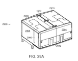
- FIG. 29A is a perspective view of a multimode antenna structure 2900 comprising a multi-band diversity receive antenna system that utilizes the band-rejection slot technique in the GPS band in accordance with one or more further embodiments of the invention.
- the GPS band is 1575.42 MHz with 20 MHz bandwidth.
- the antenna structure 2900 is formed on a flex film dielectric substrate 2902 , which is formed as a layer on a dielectric carrier 2904 .
- the antenna structure 2900 includes a GPS band rejection slot 2906 on the primary transmit antenna element 2908 of the antenna structure 2900 .
- the antenna structure 2900 also includes a diversity receive antenna element 2910 , and a connecting element 2912 connecting the diversity receive antenna element 2910 and the primary transmit antenna element 2908 .
- a GPS receiver (not shown) is connected to the diversity receive antenna element 2910 .
- the primary antenna element 2908 includes the band-rejection slot 2906 and is tuned to an electrical quarter wave length near the center of the GPS band.
- the diversity receive antenna element 2910 does not contain such a band rejection slot, but comprises a GPS antenna element that is properly matched to the main antenna source impedance so that there will be generally maximum power transfer between it and the GPS receiver.
- both antenna elements 2908 , 2910 co-exist in close proximity, the high VSWR due to the slot 2906 at the primary transmit antenna element 2908 reduces the coupling to the primary antenna element source resistance at the frequency to which the slot 2906 is tuned, and therefore provides isolation at the GPS frequency between both antenna elements 2908 , 2910 .
- the resultant mismatch between the two antenna elements 2908 , 2910 within the GPS band is large enough to decouple the antenna elements in order to meet the isolation requirements for the system design as shown in FIGS. 29B and 29C .
- FIG. 30A illustrates a multimode antenna 3000 in accordance with another embodiment of the invention.
- the antenna 3000 comprises a three mode antenna with three ports.
- three monopole antenna elements 3002 , 3004 , 3006 are connected using a connecting element 3008 which forms a conductive ring that connects neighboring antenna elements.
- the antenna elements are balanced by a common counterpoise, or sleeve 3010 , which is a single hollow conductive cylinder.
- the antenna has three coaxial cables 3012 , 3014 , 3016 for connection of the antenna to a communications device.
- the coaxial cables 3012 , 3014 , 3016 pass through the hollow interior of the sleeve 3010 .
- the antenna assembly including the sleeve, may be constructed from a single flexible printed circuit made from, e.g., 1-mil thick polyimide material with 1 ⁇ 2-ounce copper.
- the flexible printed circuit may be wrapped onto a cylinder (not shown in FIG. 30A for ease of illustration) and may be packaged in a cylindrical plastic enclosure to provide a single antenna assembly that can take the place of three separate antennas.
- the isolation between the antenna ports is dependent at least partially on the characteristics of the connecting ring 3008 including the width of the ring and amount of meandering. These parameters may be adjusted to optimize the antenna performance for a particular application.
- the input impedance at the point of connection of the coaxial cable will generally be capacitive and of high impedance compared to 50 ohm system when the ports are highly isolated.
- the input impedance may be transformed by using a matching network such as with lumped inductor and capacitor elements as known in the art.
- a modified feed geometry it is also possible to use a modified feed geometry to obtain a good match to 50 ohms without the use of lumped matching elements.
- An exemplary arrangement is for this is to use an inductive trace 3018 to transfer the feed point to a location further into the antenna.
- This technique simultaneously applies series inductance and impedance transformation to the feed to yield a good match to 50-ohms at the point of connection of the coaxial cable.
- the use of the quarter-wave sleeve 3010 and the routing of the cables through the center of the sleeve serve to decouple the cables from the antenna.
- some residual coupling between the antenna and the outside of the coaxial cable shields may occur. Excitation of currents on the outside of the coaxial cable shields may cause radiation from the shields thereby affecting the antenna pattern or may introduce additional losses via conducted paths from cables, either of which is generally undesirable.
- additional quarter-wave choke 3020 may be used beneath the antenna.
- the choke 3020 is formed from a hollow conductive cylinder that is open at the top (the end nearer to the antenna) and closed at the bottom.
- the cable shields and the choke are electrically-connected at a common point where the cables pass out the bottom of the choke as shown on FIG. 30B .
- the open end of the choke presents a high impedance to either common mode or differential mode (between cables) signals that would be conducted down the cables.
- FIGS. 30C through 30I present measured performance of one exemplary arrangement, where the diameter of the cylinder is 12 mm and the distance from the top of the antenna elements 3002 , 3004 , 3006 and the bottom of the sleeve 3010 was 39 mm so as to operate with high isolation between ports at 2.5 GHz.
- each port advantageously produces a different gain pattern as shown on FIG. 30G .
- Port 1 is the connection to element 3002 as shown in the orientation of FIG. 30A .
- the maximum gain occurs in the direction opposite of the point of connection, with each antenna port producing nominally the same cardioid radiation pattern rotated by 120 degrees.
- FIGS. 30H and 30I compare the radiation patterns from port 1 produced with and without the additional cable choke 3020 . This demonstrates the improved uniformity and pattern smoothness obtained with the addition of the choke.
- FIG. 311A illustrates a multimode antenna 3100 in accordance with another embodiment of the invention.
- the antenna 3100 comprises a three mode antenna with three ports.
- three monopole antenna elements 3102 , 3104 , 3106 are connected via connecting elements 3108 , 3110 , 3112 .
- three coplanar tabs 3114 , 3116 , 3118 serve as the connection points to the antenna and are suitable for solder connection to a printed circuit board (PCB) assembly.
- PCB printed circuit board
- the geometry of the antenna is such that the antenna can preferably be cut and formed from a single sheet of metal, e.g., 0.2 mm thick copper alloy material.
- the antenna tabs 3114 , 3116 , 3118 may be attached to a PCB 3120 as shown on FIG. 31B such the antenna extends from one edge of the PCB.
- the PCB has at least one RF ground layer that serves as a counterpoise to the antenna but also may be used to provide matching circuitry for each of the antenna ports and may also hold other components including communications circuitry for an electronic device.
- FIGS. 31C through 31G present simulated performance of one exemplary arrangement designed so as to operate in the frequency region near 2.5 GHz.
- the length of the antenna from the edge of the PCB is 28 mm and the width is 22 mm and the size of the PCB is 50 by 50 mm.
- the feed tabs 3114 , 3116 , and 3118 are connected to ports 3 , 2 , and 1 , respectively.
- Each of the three antenna ports provides an antenna mode with advantageously low VSWR, low port-to-port coupling, and high radiation efficiency.
- each port produces a unique gain pattern with low correlation to either of the other antenna patterns.
- FIG. 32A illustrates a multimode antenna 3200 in accordance with another embodiment of the invention.
- the antenna 3200 comprises a multimode antenna with three ports.
- Each antenna element 3202 has two branches to create resonance at two different frequencies with the longer branch associated with a lower resonant frequency and the shorter branch associated with a higher resonant frequency.
- the antenna elements are connected together into one structure by meandering elements 3204 between antenna elements.
- the antenna elements are balanced by a common counterpoise, or sleeve 3206 , which is a single hollow conductive cylinder.
- the antenna has three coaxial cables 3212 , 3214 , 3216 for connection of the antenna to a communications device.
- the shields of the coaxial cables are electrically attached to the sleeve while the center conductors are attached to the bottom of the antenna at points 3210 on each of the antenna elements.
- the coaxial cables 3212 , 3214 , 3216 pass through the hollow interior of the sleeve 3206 .
- the antenna assembly, including the sleeve may be constructed from a single flexible printed circuit 3208 made from, e.g., 1-mil thick polyimide material with 1 ⁇ 2-ounce copper.
- the flexible printed circuit may be wrapped into a cylinder and may be packaged in a cylindrical plastic enclosures 3218 , 3220 as shown on FIG. 32B and FIG. 32C , respectively, to provide a single antenna assembly that takes the place of three separate antennas.
- FIGS. 32D through 32H present measured performance of one exemplary arrangement designed so as to operate in the frequency bands 2.4 to 2.5 GHz and 5.15 to 5.85 GHz.
- Each of the three antenna ports provides an antenna mode with advantageously low VSWR, low port-to-port coupling, and high radiation efficiency.
- each port produces a unique gain pattern with low correlation to either of the other antenna patterns.
- FIG. 33A illustrates a multimode antenna 3300 in accordance with another embodiment of the invention.
- the antenna 3300 comprises a multimode antenna with four ports.
- the antenna elements 3302 , 3304 , 3306 , 3308 are connected together into one structure by a spoke-like cross member 3310 .
- the antenna elements are balanced by a common counterpoise, or sleeve 3312 , which is a single hollow conductive cylinder.
- FIG. 30A It is possible to use a structure of the form of FIG. 30A where neighboring antenna elements are connected by elements that follow the circumference of the cylinder, but with four monopole elements instead of three.
- the isolation is different for the case of neighboring antenna ports than it is for the case of antenna ports positioned across from each other.
- One reason for this is the physical distances between the ports in the two cases are different.
- Another reason is the connection between antenna elements does not provide a direct path between antenna elements on opposite sides of the structure. Instead, the connection path is through the neighboring antenna elements and therefore if the geometry is optimized for isolation between ports on opposite sides, then isolation between neighboring ports is not optimal.
- the difference in isolation generally prevents all four ports from achieving optimal isolation at the same frequency.
- An improved solution is achieved by using an interconnection between elements that passes through the center axis of the antenna as the spoke-like cross member 3310 of FIG. 33A . This structure achieves better uniformity of isolation response between all of the ports.
- the antenna of FIG. 33A may be constructed from a single flexible printed circuit made from, e.g., 1-mil thick polyimide material with 1 ⁇ 2-ounce copper.
- the flexible printed circuit may be wrapped on a cylinder. Slots in each of the antenna elements 3302 , 3304 , 3306 , 3308 allow the cross member 3310 to be inserted into position from the top and soldered to the antenna.
- Cross member 3310 may be formed from sheet metal, e.g., 0.2 mm thick copper alloy material. Alternately, the entire structure can be stamped from a sheet of metal and folded into the configuration shown.
- Coaxial cables may be attached to the feed points 3314 , 3316 , 3318 , 3320 on the inside of the antenna to provide means to connect the antenna to a communications device.
- the antenna has a section of narrow conductor at each of the feed attachment points, which serves to match the input impedance to 50 ohms as described above.
- FIGS. 33B , 33 C, and 33 D present measured performance of one exemplary arrangement designed so as to operate in the frequency bands from 5.15 to 5.85 GHz.
- Each of the antenna ports provides an antenna mode with advantageously low VSWR, low port-to-port coupling, and high radiation efficiency.
- each port produces a unique gain pattern with low correlation to either of the other antenna patterns.
- FIGS. 34A , 34 B, and 34 C illustrate a multimode antenna 3400 in accordance with one or more alternate embodiments of the invention.
- the antenna 3400 includes two antenna elements 3402 , 3404 which wrap from the top side as shown on FIG. 34B to the bottom side as shown on FIG. 34C .
- the bottom side includes connecting element 3406 and feed points 3408 and 3410 .
- the bottom surface provides a means of support and electrical connection to a PCB assembly.
- the antenna 3400 can be manufactured, e.g., by metal stamping. It can be made, e.g., from 0.2 mm thick copper alloy sheet.
- the antenna does not require any additional supporting or dielectric materials.
- the antenna is also compatible with surface-mount reflow assembly.
- the antenna 3400 can be used, e.g., in a WIMAX USB dongle using WiMAX bands from 2500 to 2700 MHz.
- An exemplary assembly of this type, used for testing and evaluation of antenna 3400 is shown on FIG. 34D .
- the test PCB assembly 3420 includes two-component lumped element match networks for each of the antenna ports.
- FIGS. 34E to 34N present measured performance the test assembly 3420 .
- Each of the antenna ports provides an antenna mode with advantageously low VSWR, low port-to-port coupling, and high radiation efficiency.
- each port produces a unique gain pattern with low correlation to either of the other antenna patterns.
- FIG. 35A illustrates a multimode antenna 3500 in accordance with one or more alternate embodiments of the invention.
- the antenna 3500 includes two antenna elements 3502 , 3504 and connecting portion 3506 comprised of two strips.
- the antenna has two feed points 3508 , 3510 at the bottom.
- the bottom surface provides a means of support and electrical connection to a PCB assembly.
- the antenna 3500 can be manufactured, e.g., by metal stamping. It can be made, e.g., from 0.2 mm thick copper alloy sheet.
- the antenna does not require any additional supporting or dielectric materials.
- the antenna is also compatible with surface-mount reflow assembly.
- the antenna 3500 is designed for use in two frequency bands. This is achieved by the meandered structure of elements 3502 , 3504 .
- the elements support a lower frequency resonance via the longer inductive path of the conductor and a second higher frequency resonance along the coupled path across the gaps between the meanders as illustrated on FIG. 35B .
- the antenna 3500 can be used, e.g., in an 802.11a/b/g/n enabled device with operable frequency bands from 2400 to 2500 MHz and 4900 to 6000 MHz.
- An exemplary assembly of this type, used for testing and evaluation of antenna 3500 is shown on FIG. 35C .
- the test PCB assembly 3520 includes two-component lumped element match networks for each of the antenna ports.
- FIGS. 35D through 35K present simulated performance the test assembly 3520 .
- Each of the antenna ports provides an antenna mode with advantageously low VSWR, low port-to-port coupling, and high radiation efficiency.
- each port produces a unique gain pattern with low correlation to either of the other antenna patterns.
- FIG. 36A illustrates a multimode antenna 3600 in accordance with another embodiment of the invention.
- the antenna 3600 comprises a multimode antenna with four ports.
- Each antenna element 3602 has two branches to create resonance at two different frequencies with the longer branch associated with a lower resonant frequency and the shorter branch associated with a higher resonant frequency.
- the antenna elements are connected together into one structure by a spoke-like cross member 3612 between antenna elements.
- the antenna elements are balanced by a common counterpoise, or sleeve 3610 , which is a single hollow conductive cylinder.
- the antenna of FIG. 36A may be constructed from a single flexible printed circuit wrapped into a cylinder.
- the spoke-like cross member 3610 may be electrically attached, e.g., by being soldered to the flexible printed circuit.
- Cross member may be formed from sheet metal, e.g., 0.2 mm thick copper alloy material.
- Coaxial cables may be attached to the feed points on the inside of the antenna to provide means to connect the antenna to a communications device.
- FIGS. 36B and 36C present simulated VSWR and realized radiation efficiency of one exemplary arrangement designed so as to operate in the frequency bands 2.4 to 2.5 GHz and 5.15 to 5.85 GHz.
- each of the antenna structures can be configured to include any number of antenna elements connected by connecting elements.
- the antennas shown in FIGS. 30 , 32 , 33 , and 36 can have either a cylindrical configuration or a polyhedral configuration (i.e., having multiple planar faces).
- the antenna elements and the connecting elements preferably form a single integrated radiating structure such that a signal fed to either port excites the entire antenna to radiate as a whole, rather than separate radiating structures.
- the techniques described herein provide isolation of the antenna ports without the use of decoupling networks at the antenna feed points.
Abstract
Description
where β=2π/λ, N=Total # of elements, α=phase shift between successive elements, and θ=angle from array axis
Claims (30)
Priority Applications (4)
| Application Number | Priority Date | Filing Date | Title |
|---|---|---|---|
| US12/727,531 US8866691B2 (en) | 2007-04-20 | 2010-03-19 | Multimode antenna structure |
| US14/450,365 US9190726B2 (en) | 2007-04-20 | 2014-08-04 | Multimode antenna structure |
| US14/918,895 US9401547B2 (en) | 2007-04-20 | 2015-10-21 | Multimode antenna structure |
| US15/190,870 US20170149146A1 (en) | 2007-04-20 | 2016-06-23 | Multimode antenna structure |
Applications Claiming Priority (6)
| Application Number | Priority Date | Filing Date | Title |
|---|---|---|---|
| US92539407P | 2007-04-20 | 2007-04-20 | |
| US91665507P | 2007-05-08 | 2007-05-08 | |
| US11/769,565 US7688275B2 (en) | 2007-04-20 | 2007-06-27 | Multimode antenna structure |
| US12/099,320 US7688273B2 (en) | 2007-04-20 | 2008-04-08 | Multimode antenna structure |
| US16166909P | 2009-03-19 | 2009-03-19 | |
| US12/727,531 US8866691B2 (en) | 2007-04-20 | 2010-03-19 | Multimode antenna structure |
Related Parent Applications (1)
| Application Number | Title | Priority Date | Filing Date |
|---|---|---|---|
| US12/099,320 Continuation-In-Part US7688273B2 (en) | 2007-04-20 | 2008-04-08 | Multimode antenna structure |
Related Child Applications (1)
| Application Number | Title | Priority Date | Filing Date |
|---|---|---|---|
| US14/450,365 Continuation US9190726B2 (en) | 2007-04-20 | 2014-08-04 | Multimode antenna structure |
Publications (2)
| Publication Number | Publication Date |
|---|---|
| US20100265146A1 US20100265146A1 (en) | 2010-10-21 |
| US8866691B2 true US8866691B2 (en) | 2014-10-21 |
Family
ID=42980624
Family Applications (4)
| Application Number | Title | Priority Date | Filing Date |
|---|---|---|---|
| US12/727,531 Expired - Fee Related US8866691B2 (en) | 2007-04-20 | 2010-03-19 | Multimode antenna structure |
| US14/450,365 Expired - Fee Related US9190726B2 (en) | 2007-04-20 | 2014-08-04 | Multimode antenna structure |
| US14/918,895 Expired - Fee Related US9401547B2 (en) | 2007-04-20 | 2015-10-21 | Multimode antenna structure |
| US15/190,870 Abandoned US20170149146A1 (en) | 2007-04-20 | 2016-06-23 | Multimode antenna structure |
Family Applications After (3)
| Application Number | Title | Priority Date | Filing Date |
|---|---|---|---|
| US14/450,365 Expired - Fee Related US9190726B2 (en) | 2007-04-20 | 2014-08-04 | Multimode antenna structure |
| US14/918,895 Expired - Fee Related US9401547B2 (en) | 2007-04-20 | 2015-10-21 | Multimode antenna structure |
| US15/190,870 Abandoned US20170149146A1 (en) | 2007-04-20 | 2016-06-23 | Multimode antenna structure |
Country Status (1)
| Country | Link |
|---|---|
| US (4) | US8866691B2 (en) |
Cited By (154)
| Publication number | Priority date | Publication date | Assignee | Title |
|---|---|---|---|---|
| US20140159986A1 (en) * | 2012-12-06 | 2014-06-12 | Microsoft Corporation | Reconfigurable multiband antenna decoupling networks |
| US20140340269A1 (en) * | 2007-04-20 | 2014-11-20 | Skycross, Inc. | Multimode antenna structure |
| US20150120189A1 (en) * | 2013-10-28 | 2015-04-30 | Skycross, Inc. | Antenna structures and methods thereof for determining locations to improve wireless communications |
| US9318803B2 (en) | 2007-04-20 | 2016-04-19 | Skycross, Inc. | Multimode antenna structure |
| US9337548B2 (en) | 2007-04-20 | 2016-05-10 | Skycross, Inc. | Methods for reducing near-field radiation and specific absorption rate (SAR) values in communications devices |
| US9608740B2 (en) | 2015-07-15 | 2017-03-28 | At&T Intellectual Property I, L.P. | Method and apparatus for launching a wave mode that mitigates interference |
| US9615269B2 (en) | 2014-10-02 | 2017-04-04 | At&T Intellectual Property I, L.P. | Method and apparatus that provides fault tolerance in a communication network |
| US9628116B2 (en) | 2015-07-14 | 2017-04-18 | At&T Intellectual Property I, L.P. | Apparatus and methods for transmitting wireless signals |
| US9640850B2 (en) | 2015-06-25 | 2017-05-02 | At&T Intellectual Property I, L.P. | Methods and apparatus for inducing a non-fundamental wave mode on a transmission medium |
| US9667317B2 (en) | 2015-06-15 | 2017-05-30 | At&T Intellectual Property I, L.P. | Method and apparatus for providing security using network traffic adjustments |
| US9674711B2 (en) | 2013-11-06 | 2017-06-06 | At&T Intellectual Property I, L.P. | Surface-wave communications and methods thereof |
| US9685992B2 (en) | 2014-10-03 | 2017-06-20 | At&T Intellectual Property I, L.P. | Circuit panel network and methods thereof |
| US9692101B2 (en) | 2014-08-26 | 2017-06-27 | At&T Intellectual Property I, L.P. | Guided wave couplers for coupling electromagnetic waves between a waveguide surface and a surface of a wire |
| US9699785B2 (en) | 2012-12-05 | 2017-07-04 | At&T Intellectual Property I, L.P. | Backhaul link for distributed antenna system |
| US9705610B2 (en) | 2014-10-21 | 2017-07-11 | At&T Intellectual Property I, L.P. | Transmission device with impairment compensation and methods for use therewith |
| US9705561B2 (en) | 2015-04-24 | 2017-07-11 | At&T Intellectual Property I, L.P. | Directional coupling device and methods for use therewith |
| US9722318B2 (en) | 2015-07-14 | 2017-08-01 | At&T Intellectual Property I, L.P. | Method and apparatus for coupling an antenna to a device |
| US9729197B2 (en) | 2015-10-01 | 2017-08-08 | At&T Intellectual Property I, L.P. | Method and apparatus for communicating network management traffic over a network |
| US9735833B2 (en) | 2015-07-31 | 2017-08-15 | At&T Intellectual Property I, L.P. | Method and apparatus for communications management in a neighborhood network |
| US9742521B2 (en) | 2014-11-20 | 2017-08-22 | At&T Intellectual Property I, L.P. | Transmission device with mode division multiplexing and methods for use therewith |
| US9742462B2 (en) | 2014-12-04 | 2017-08-22 | At&T Intellectual Property I, L.P. | Transmission medium and communication interfaces and methods for use therewith |
| US9748626B2 (en) | 2015-05-14 | 2017-08-29 | At&T Intellectual Property I, L.P. | Plurality of cables having different cross-sectional shapes which are bundled together to form a transmission medium |
| US9749013B2 (en) | 2015-03-17 | 2017-08-29 | At&T Intellectual Property I, L.P. | Method and apparatus for reducing attenuation of electromagnetic waves guided by a transmission medium |
| US9749053B2 (en) | 2015-07-23 | 2017-08-29 | At&T Intellectual Property I, L.P. | Node device, repeater and methods for use therewith |
| US9762289B2 (en) | 2014-10-14 | 2017-09-12 | At&T Intellectual Property I, L.P. | Method and apparatus for transmitting or receiving signals in a transportation system |
| US9769020B2 (en) | 2014-10-21 | 2017-09-19 | At&T Intellectual Property I, L.P. | Method and apparatus for responding to events affecting communications in a communication network |
| US9769128B2 (en) | 2015-09-28 | 2017-09-19 | At&T Intellectual Property I, L.P. | Method and apparatus for encryption of communications over a network |
| US9768833B2 (en) | 2014-09-15 | 2017-09-19 | At&T Intellectual Property I, L.P. | Method and apparatus for sensing a condition in a transmission medium of electromagnetic waves |
| US9780834B2 (en) | 2014-10-21 | 2017-10-03 | At&T Intellectual Property I, L.P. | Method and apparatus for transmitting electromagnetic waves |
| US9787412B2 (en) | 2015-06-25 | 2017-10-10 | At&T Intellectual Property I, L.P. | Methods and apparatus for inducing a fundamental wave mode on a transmission medium |
| US9793954B2 (en) | 2015-04-28 | 2017-10-17 | At&T Intellectual Property I, L.P. | Magnetic coupling device and methods for use therewith |
| US9793955B2 (en) | 2015-04-24 | 2017-10-17 | At&T Intellectual Property I, Lp | Passive electrical coupling device and methods for use therewith |
| US9793951B2 (en) | 2015-07-15 | 2017-10-17 | At&T Intellectual Property I, L.P. | Method and apparatus for launching a wave mode that mitigates interference |
| US9800327B2 (en) | 2014-11-20 | 2017-10-24 | At&T Intellectual Property I, L.P. | Apparatus for controlling operations of a communication device and methods thereof |
| US9820146B2 (en) | 2015-06-12 | 2017-11-14 | At&T Intellectual Property I, L.P. | Method and apparatus for authentication and identity management of communicating devices |
| US9838896B1 (en) | 2016-12-09 | 2017-12-05 | At&T Intellectual Property I, L.P. | Method and apparatus for assessing network coverage |
| US9838078B2 (en) | 2015-07-31 | 2017-12-05 | At&T Intellectual Property I, L.P. | Method and apparatus for exchanging communication signals |
| US9847566B2 (en) | 2015-07-14 | 2017-12-19 | At&T Intellectual Property I, L.P. | Method and apparatus for adjusting a field of a signal to mitigate interference |
| US9847850B2 (en) | 2014-10-14 | 2017-12-19 | At&T Intellectual Property I, L.P. | Method and apparatus for adjusting a mode of communication in a communication network |
| US9853342B2 (en) | 2015-07-14 | 2017-12-26 | At&T Intellectual Property I, L.P. | Dielectric transmission medium connector and methods for use therewith |
| US9860075B1 (en) | 2016-08-26 | 2018-01-02 | At&T Intellectual Property I, L.P. | Method and communication node for broadband distribution |
| US9866276B2 (en) | 2014-10-10 | 2018-01-09 | At&T Intellectual Property I, L.P. | Method and apparatus for arranging communication sessions in a communication system |
| US9866309B2 (en) | 2015-06-03 | 2018-01-09 | At&T Intellectual Property I, Lp | Host node device and methods for use therewith |
| US9865911B2 (en) | 2015-06-25 | 2018-01-09 | At&T Intellectual Property I, L.P. | Waveguide system for slot radiating first electromagnetic waves that are combined into a non-fundamental wave mode second electromagnetic wave on a transmission medium |
| US9871282B2 (en) | 2015-05-14 | 2018-01-16 | At&T Intellectual Property I, L.P. | At least one transmission medium having a dielectric surface that is covered at least in part by a second dielectric |
| US9871558B2 (en) | 2014-10-21 | 2018-01-16 | At&T Intellectual Property I, L.P. | Guided-wave transmission device and methods for use therewith |
| US9871283B2 (en) | 2015-07-23 | 2018-01-16 | At&T Intellectual Property I, Lp | Transmission medium having a dielectric core comprised of plural members connected by a ball and socket configuration |
| US9876264B2 (en) | 2015-10-02 | 2018-01-23 | At&T Intellectual Property I, Lp | Communication system, guided wave switch and methods for use therewith |
| US9876570B2 (en) | 2015-02-20 | 2018-01-23 | At&T Intellectual Property I, Lp | Guided-wave transmission device with non-fundamental mode propagation and methods for use therewith |
| US9876605B1 (en) | 2016-10-21 | 2018-01-23 | At&T Intellectual Property I, L.P. | Launcher and coupling system to support desired guided wave mode |
| US9882257B2 (en) | 2015-07-14 | 2018-01-30 | At&T Intellectual Property I, L.P. | Method and apparatus for launching a wave mode that mitigates interference |
| US9887447B2 (en) | 2015-05-14 | 2018-02-06 | At&T Intellectual Property I, L.P. | Transmission medium having multiple cores and methods for use therewith |
| US9893795B1 (en) | 2016-12-07 | 2018-02-13 | At&T Intellectual Property I, Lp | Method and repeater for broadband distribution |
| US9904535B2 (en) | 2015-09-14 | 2018-02-27 | At&T Intellectual Property I, L.P. | Method and apparatus for distributing software |
| US9906269B2 (en) | 2014-09-17 | 2018-02-27 | At&T Intellectual Property I, L.P. | Monitoring and mitigating conditions in a communication network |
| US9912033B2 (en) | 2014-10-21 | 2018-03-06 | At&T Intellectual Property I, Lp | Guided wave coupler, coupling module and methods for use therewith |
| US9912027B2 (en) | 2015-07-23 | 2018-03-06 | At&T Intellectual Property I, L.P. | Method and apparatus for exchanging communication signals |
| US9913139B2 (en) | 2015-06-09 | 2018-03-06 | At&T Intellectual Property I, L.P. | Signal fingerprinting for authentication of communicating devices |
| US9912381B2 (en) | 2015-06-03 | 2018-03-06 | At&T Intellectual Property I, Lp | Network termination and methods for use therewith |
| US9911020B1 (en) | 2016-12-08 | 2018-03-06 | At&T Intellectual Property I, L.P. | Method and apparatus for tracking via a radio frequency identification device |
| US9912419B1 (en) | 2016-08-24 | 2018-03-06 | At&T Intellectual Property I, L.P. | Method and apparatus for managing a fault in a distributed antenna system |
| US9917341B2 (en) | 2015-05-27 | 2018-03-13 | At&T Intellectual Property I, L.P. | Apparatus and method for launching electromagnetic waves and for modifying radial dimensions of the propagating electromagnetic waves |
| US9927517B1 (en) | 2016-12-06 | 2018-03-27 | At&T Intellectual Property I, L.P. | Apparatus and methods for sensing rainfall |
| US9930668B2 (en) | 2013-05-31 | 2018-03-27 | At&T Intellectual Property I, L.P. | Remote distributed antenna system |
| US9948355B2 (en) | 2014-10-21 | 2018-04-17 | At&T Intellectual Property I, L.P. | Apparatus for providing communication services and methods thereof |
| US9948354B2 (en) | 2015-04-28 | 2018-04-17 | At&T Intellectual Property I, L.P. | Magnetic coupling device with reflective plate and methods for use therewith |
| US9948333B2 (en) | 2015-07-23 | 2018-04-17 | At&T Intellectual Property I, L.P. | Method and apparatus for wireless communications to mitigate interference |
| US9954287B2 (en) | 2014-11-20 | 2018-04-24 | At&T Intellectual Property I, L.P. | Apparatus for converting wireless signals and electromagnetic waves and methods thereof |
| US9954286B2 (en) | 2014-10-21 | 2018-04-24 | At&T Intellectual Property I, L.P. | Guided-wave transmission device with non-fundamental mode propagation and methods for use therewith |
| US9967173B2 (en) | 2015-07-31 | 2018-05-08 | At&T Intellectual Property I, L.P. | Method and apparatus for authentication and identity management of communicating devices |
| US9973940B1 (en) | 2017-02-27 | 2018-05-15 | At&T Intellectual Property I, L.P. | Apparatus and methods for dynamic impedance matching of a guided wave launcher |
| US9991580B2 (en) | 2016-10-21 | 2018-06-05 | At&T Intellectual Property I, L.P. | Launcher and coupling system for guided wave mode cancellation |
| US9999038B2 (en) | 2013-05-31 | 2018-06-12 | At&T Intellectual Property I, L.P. | Remote distributed antenna system |
| US9998870B1 (en) | 2016-12-08 | 2018-06-12 | At&T Intellectual Property I, L.P. | Method and apparatus for proximity sensing |
| US9997819B2 (en) | 2015-06-09 | 2018-06-12 | At&T Intellectual Property I, L.P. | Transmission medium and method for facilitating propagation of electromagnetic waves via a core |
| US10009065B2 (en) | 2012-12-05 | 2018-06-26 | At&T Intellectual Property I, L.P. | Backhaul link for distributed antenna system |
| US10009067B2 (en) | 2014-12-04 | 2018-06-26 | At&T Intellectual Property I, L.P. | Method and apparatus for configuring a communication interface |
| US10009063B2 (en) | 2015-09-16 | 2018-06-26 | At&T Intellectual Property I, L.P. | Method and apparatus for use with a radio distributed antenna system having an out-of-band reference signal |
| US10020844B2 (en) | 2016-12-06 | 2018-07-10 | T&T Intellectual Property I, L.P. | Method and apparatus for broadcast communication via guided waves |
| US10027397B2 (en) | 2016-12-07 | 2018-07-17 | At&T Intellectual Property I, L.P. | Distributed antenna system and methods for use therewith |
| US10027398B2 (en) | 2015-06-11 | 2018-07-17 | At&T Intellectual Property I, Lp | Repeater and methods for use therewith |
| US10033108B2 (en) | 2015-07-14 | 2018-07-24 | At&T Intellectual Property I, L.P. | Apparatus and methods for generating an electromagnetic wave having a wave mode that mitigates interference |
| US10033107B2 (en) | 2015-07-14 | 2018-07-24 | At&T Intellectual Property I, L.P. | Method and apparatus for coupling an antenna to a device |
| US10044409B2 (en) | 2015-07-14 | 2018-08-07 | At&T Intellectual Property I, L.P. | Transmission medium and methods for use therewith |
| US10069535B2 (en) | 2016-12-08 | 2018-09-04 | At&T Intellectual Property I, L.P. | Apparatus and methods for launching electromagnetic waves having a certain electric field structure |
| US10079661B2 (en) | 2015-09-16 | 2018-09-18 | At&T Intellectual Property I, L.P. | Method and apparatus for use with a radio distributed antenna system having a clock reference |
| US10090594B2 (en) | 2016-11-23 | 2018-10-02 | At&T Intellectual Property I, L.P. | Antenna system having structural configurations for assembly |
| US10090606B2 (en) | 2015-07-15 | 2018-10-02 | At&T Intellectual Property I, L.P. | Antenna system with dielectric array and methods for use therewith |
| US10103422B2 (en) | 2016-12-08 | 2018-10-16 | At&T Intellectual Property I, L.P. | Method and apparatus for mounting network devices |
| US10103801B2 (en) | 2015-06-03 | 2018-10-16 | At&T Intellectual Property I, L.P. | Host node device and methods for use therewith |
| US10135147B2 (en) | 2016-10-18 | 2018-11-20 | At&T Intellectual Property I, L.P. | Apparatus and methods for launching guided waves via an antenna |
| US10135145B2 (en) | 2016-12-06 | 2018-11-20 | At&T Intellectual Property I, L.P. | Apparatus and methods for generating an electromagnetic wave along a transmission medium |
| US10136434B2 (en) | 2015-09-16 | 2018-11-20 | At&T Intellectual Property I, L.P. | Method and apparatus for use with a radio distributed antenna system having an ultra-wideband control channel |
| US10135146B2 (en) | 2016-10-18 | 2018-11-20 | At&T Intellectual Property I, L.P. | Apparatus and methods for launching guided waves via circuits |
| US10139820B2 (en) | 2016-12-07 | 2018-11-27 | At&T Intellectual Property I, L.P. | Method and apparatus for deploying equipment of a communication system |
| US10142086B2 (en) | 2015-06-11 | 2018-11-27 | At&T Intellectual Property I, L.P. | Repeater and methods for use therewith |
| US10148016B2 (en) | 2015-07-14 | 2018-12-04 | At&T Intellectual Property I, L.P. | Apparatus and methods for communicating utilizing an antenna array |
| US10144036B2 (en) | 2015-01-30 | 2018-12-04 | At&T Intellectual Property I, L.P. | Method and apparatus for mitigating interference affecting a propagation of electromagnetic waves guided by a transmission medium |
| US10170840B2 (en) | 2015-07-14 | 2019-01-01 | At&T Intellectual Property I, L.P. | Apparatus and methods for sending or receiving electromagnetic signals |
| US10168695B2 (en) | 2016-12-07 | 2019-01-01 | At&T Intellectual Property I, L.P. | Method and apparatus for controlling an unmanned aircraft |
| US10178445B2 (en) | 2016-11-23 | 2019-01-08 | At&T Intellectual Property I, L.P. | Methods, devices, and systems for load balancing between a plurality of waveguides |
| US10205655B2 (en) | 2015-07-14 | 2019-02-12 | At&T Intellectual Property I, L.P. | Apparatus and methods for communicating utilizing an antenna array and multiple communication paths |
| US10225025B2 (en) | 2016-11-03 | 2019-03-05 | At&T Intellectual Property I, L.P. | Method and apparatus for detecting a fault in a communication system |
| US10224634B2 (en) | 2016-11-03 | 2019-03-05 | At&T Intellectual Property I, L.P. | Methods and apparatus for adjusting an operational characteristic of an antenna |
| US10243270B2 (en) | 2016-12-07 | 2019-03-26 | At&T Intellectual Property I, L.P. | Beam adaptive multi-feed dielectric antenna system and methods for use therewith |
| US10243784B2 (en) | 2014-11-20 | 2019-03-26 | At&T Intellectual Property I, L.P. | System for generating topology information and methods thereof |
| US10264586B2 (en) | 2016-12-09 | 2019-04-16 | At&T Mobility Ii Llc | Cloud-based packet controller and methods for use therewith |
| US10291311B2 (en) | 2016-09-09 | 2019-05-14 | At&T Intellectual Property I, L.P. | Method and apparatus for mitigating a fault in a distributed antenna system |
| US10291334B2 (en) | 2016-11-03 | 2019-05-14 | At&T Intellectual Property I, L.P. | System for detecting a fault in a communication system |
| US10298293B2 (en) | 2017-03-13 | 2019-05-21 | At&T Intellectual Property I, L.P. | Apparatus of communication utilizing wireless network devices |
| US10305190B2 (en) | 2016-12-01 | 2019-05-28 | At&T Intellectual Property I, L.P. | Reflecting dielectric antenna system and methods for use therewith |
| US10312567B2 (en) | 2016-10-26 | 2019-06-04 | At&T Intellectual Property I, L.P. | Launcher with planar strip antenna and methods for use therewith |
| US10320586B2 (en) | 2015-07-14 | 2019-06-11 | At&T Intellectual Property I, L.P. | Apparatus and methods for generating non-interfering electromagnetic waves on an insulated transmission medium |
| US10326494B2 (en) | 2016-12-06 | 2019-06-18 | At&T Intellectual Property I, L.P. | Apparatus for measurement de-embedding and methods for use therewith |
| US10326689B2 (en) | 2016-12-08 | 2019-06-18 | At&T Intellectual Property I, L.P. | Method and system for providing alternative communication paths |
| US10340603B2 (en) | 2016-11-23 | 2019-07-02 | At&T Intellectual Property I, L.P. | Antenna system having shielded structural configurations for assembly |
| US10341142B2 (en) | 2015-07-14 | 2019-07-02 | At&T Intellectual Property I, L.P. | Apparatus and methods for generating non-interfering electromagnetic waves on an uninsulated conductor |
| US10340600B2 (en) | 2016-10-18 | 2019-07-02 | At&T Intellectual Property I, L.P. | Apparatus and methods for launching guided waves via plural waveguide systems |
| US10340601B2 (en) | 2016-11-23 | 2019-07-02 | At&T Intellectual Property I, L.P. | Multi-antenna system and methods for use therewith |
| US10340573B2 (en) | 2016-10-26 | 2019-07-02 | At&T Intellectual Property I, L.P. | Launcher with cylindrical coupling device and methods for use therewith |
| US10340983B2 (en) | 2016-12-09 | 2019-07-02 | At&T Intellectual Property I, L.P. | Method and apparatus for surveying remote sites via guided wave communications |
| US10355367B2 (en) | 2015-10-16 | 2019-07-16 | At&T Intellectual Property I, L.P. | Antenna structure for exchanging wireless signals |
| US10359749B2 (en) | 2016-12-07 | 2019-07-23 | At&T Intellectual Property I, L.P. | Method and apparatus for utilities management via guided wave communication |
| US10361489B2 (en) | 2016-12-01 | 2019-07-23 | At&T Intellectual Property I, L.P. | Dielectric dish antenna system and methods for use therewith |
| US10374316B2 (en) | 2016-10-21 | 2019-08-06 | At&T Intellectual Property I, L.P. | System and dielectric antenna with non-uniform dielectric |
| US10382976B2 (en) | 2016-12-06 | 2019-08-13 | At&T Intellectual Property I, L.P. | Method and apparatus for managing wireless communications based on communication paths and network device positions |
| US10389037B2 (en) | 2016-12-08 | 2019-08-20 | At&T Intellectual Property I, L.P. | Apparatus and methods for selecting sections of an antenna array and use therewith |
| US10389029B2 (en) | 2016-12-07 | 2019-08-20 | At&T Intellectual Property I, L.P. | Multi-feed dielectric antenna system with core selection and methods for use therewith |
| US10411356B2 (en) | 2016-12-08 | 2019-09-10 | At&T Intellectual Property I, L.P. | Apparatus and methods for selectively targeting communication devices with an antenna array |
| US10439675B2 (en) | 2016-12-06 | 2019-10-08 | At&T Intellectual Property I, L.P. | Method and apparatus for repeating guided wave communication signals |
| US10446936B2 (en) | 2016-12-07 | 2019-10-15 | At&T Intellectual Property I, L.P. | Multi-feed dielectric antenna system and methods for use therewith |
| US10498044B2 (en) | 2016-11-03 | 2019-12-03 | At&T Intellectual Property I, L.P. | Apparatus for configuring a surface of an antenna |
| US10530505B2 (en) | 2016-12-08 | 2020-01-07 | At&T Intellectual Property I, L.P. | Apparatus and methods for launching electromagnetic waves along a transmission medium |
| US10535928B2 (en) | 2016-11-23 | 2020-01-14 | At&T Intellectual Property I, L.P. | Antenna system and methods for use therewith |
| US10547099B2 (en) | 2015-11-02 | 2020-01-28 | Samsung Electronics Co., Ltd. | Antenna structure and electronic device including the same |
| US10547348B2 (en) | 2016-12-07 | 2020-01-28 | At&T Intellectual Property I, L.P. | Method and apparatus for switching transmission mediums in a communication system |
| US10601494B2 (en) | 2016-12-08 | 2020-03-24 | At&T Intellectual Property I, L.P. | Dual-band communication device and method for use therewith |
| US10637149B2 (en) | 2016-12-06 | 2020-04-28 | At&T Intellectual Property I, L.P. | Injection molded dielectric antenna and methods for use therewith |
| US10650940B2 (en) | 2015-05-15 | 2020-05-12 | At&T Intellectual Property I, L.P. | Transmission medium having a conductive material and methods for use therewith |
| US10665942B2 (en) | 2015-10-16 | 2020-05-26 | At&T Intellectual Property I, L.P. | Method and apparatus for adjusting wireless communications |
| US10694379B2 (en) | 2016-12-06 | 2020-06-23 | At&T Intellectual Property I, L.P. | Waveguide system with device-based authentication and methods for use therewith |
| US10727599B2 (en) | 2016-12-06 | 2020-07-28 | At&T Intellectual Property I, L.P. | Launcher with slot antenna and methods for use therewith |
| US10755542B2 (en) | 2016-12-06 | 2020-08-25 | At&T Intellectual Property I, L.P. | Method and apparatus for surveillance via guided wave communication |
| US10777873B2 (en) | 2016-12-08 | 2020-09-15 | At&T Intellectual Property I, L.P. | Method and apparatus for mounting network devices |
| US10797781B2 (en) | 2015-06-03 | 2020-10-06 | At&T Intellectual Property I, L.P. | Client node device and methods for use therewith |
| US10811767B2 (en) | 2016-10-21 | 2020-10-20 | At&T Intellectual Property I, L.P. | System and dielectric antenna with convex dielectric radome |
| US10819035B2 (en) | 2016-12-06 | 2020-10-27 | At&T Intellectual Property I, L.P. | Launcher with helical antenna and methods for use therewith |
| US10916969B2 (en) | 2016-12-08 | 2021-02-09 | At&T Intellectual Property I, L.P. | Method and apparatus for providing power using an inductive coupling |
| US10938108B2 (en) | 2016-12-08 | 2021-03-02 | At&T Intellectual Property I, L.P. | Frequency selective multi-feed dielectric antenna system and methods for use therewith |
| US11032819B2 (en) | 2016-09-15 | 2021-06-08 | At&T Intellectual Property I, L.P. | Method and apparatus for use with a radio distributed antenna system having a control channel reference signal |
| US11050136B2 (en) | 2016-09-19 | 2021-06-29 | Samsung Electronics Co., Ltd | Electronic device comprising antenna |
| US20220390497A1 (en) * | 2019-10-29 | 2022-12-08 | Nippon Telegraph And Telephone Corporation | High-Frequency Noise Detection Antenna |
| US11664589B2 (en) | 2021-03-10 | 2023-05-30 | Synergy Microwave Corporation | 5G MIMO antenna array with reduced mutual coupling |
| WO2023114361A3 (en) * | 2021-12-17 | 2023-12-21 | Bae Systems Information And Electronic Systems Integration Inc. | Collapsible monopole antenna for space-disadvantaged cylindrical platforms |
Families Citing this family (34)
| Publication number | Priority date | Publication date | Assignee | Title |
|---|---|---|---|---|
| JP4524318B2 (en) * | 2008-05-27 | 2010-08-18 | 原田工業株式会社 | Automotive noise filter |
| WO2011024355A1 (en) | 2009-08-25 | 2011-03-03 | パナソニック株式会社 | Antenna device and radio communication device |
| JP5532847B2 (en) * | 2009-11-20 | 2014-06-25 | 船井電機株式会社 | Multi-antenna device and portable device |
| JP2011176560A (en) * | 2010-02-24 | 2011-09-08 | Fujitsu Ltd | Antenna apparatus, and radio terminal apparatus |
| US8890763B2 (en) | 2011-02-21 | 2014-11-18 | Funai Electric Co., Ltd. | Multiantenna unit and communication apparatus |
| JP5424500B2 (en) | 2011-04-20 | 2014-02-26 | パナソニック株式会社 | Antenna device and portable wireless terminal equipped with the same |
| JP5511089B2 (en) | 2011-05-19 | 2014-06-04 | パナソニック株式会社 | Antenna device |
| JP5263365B2 (en) * | 2011-10-12 | 2013-08-14 | カシオ計算機株式会社 | Multi-frequency circularly polarized antenna |
| WO2013112214A2 (en) | 2011-10-18 | 2013-08-01 | California Institute Of Technology | Efficient active multi-drive radiator |
| KR101918985B1 (en) * | 2011-12-05 | 2018-11-16 | 엘지전자 주식회사 | Mobile terminal |
| WO2013123090A1 (en) | 2012-02-13 | 2013-08-22 | California Institute Of Technology | Sensing radiation metrics through mode-pickup sensors |
| US9686070B2 (en) | 2012-02-17 | 2017-06-20 | California Institute Of Technology | Dynamic polarization modulation and control |
| US9621269B2 (en) | 2012-07-26 | 2017-04-11 | California Institute Of Technology | Optically driven active radiator |
| GB201213558D0 (en) * | 2012-07-31 | 2012-09-12 | Univ Birmingham | Reconfigurable antenna |
| US20140269449A1 (en) * | 2013-03-15 | 2014-09-18 | Qualcomm Incorporated | Full-duplex wireless transceiver with hybrid circuit and reconfigurable radiation pattern antenna |
| JP6320074B2 (en) * | 2014-02-19 | 2018-05-09 | 日本アンテナ株式会社 | Antenna device |
| US9866069B2 (en) * | 2014-12-29 | 2018-01-09 | Ricoh Co., Ltd. | Manually beam steered phased array |
| GB2545918B (en) * | 2015-12-30 | 2020-01-22 | Antenova Ltd | Reconfigurable antenna |
| CN106571526A (en) * | 2016-04-06 | 2017-04-19 | 昆山睿翔讯通通信技术有限公司 | Decoupling method and decoupling network of MIMO antenna of mobile communication system terminal |
| US9972911B1 (en) | 2016-10-24 | 2018-05-15 | King Fahd University Of Petroleum And Minerals | Wide band frequency agile MIMO antenna |
| CN106450709B (en) * | 2016-12-22 | 2019-12-06 | 厦门大学 | Four-unit interconnected symmetrical oscillator circular antenna array for electric small-distance direction finding |
| GB2563574B (en) * | 2017-06-05 | 2021-08-04 | International Electric Company Ltd | A phased array antenna and apparatus incorporating the same |
| TWM568509U (en) * | 2018-07-12 | 2018-10-11 | 明泰科技股份有限公司 | Antenna module with low profile and high dual band insulation |
| TWI684302B (en) * | 2018-11-23 | 2020-02-01 | 啓碁科技股份有限公司 | Communication device and notebook computer device |
| US10923830B2 (en) * | 2019-01-18 | 2021-02-16 | Pc-Tel, Inc. | Quick solder chip connector for massive multiple-input multiple-output antenna systems |
| JP7216577B2 (en) * | 2019-03-05 | 2023-02-01 | 日本航空電子工業株式会社 | antenna |
| US11437716B1 (en) * | 2019-03-27 | 2022-09-06 | FIRST RF Corp. | Antenna element |
| JP7196008B2 (en) | 2019-04-17 | 2022-12-26 | 日本航空電子工業株式会社 | antenna |
| US20220352634A1 (en) * | 2019-06-25 | 2022-11-03 | Kyocera Corporation | Antenna, wireless communication module, and wireless communication device |
| JP7414415B2 (en) * | 2019-06-27 | 2024-01-16 | 日本航空電子工業株式会社 | Intermediate products for antennas and opposing parts used for them |
| JP7414414B2 (en) * | 2019-06-27 | 2024-01-16 | 日本航空電子工業株式会社 | antenna |
| CN115149244A (en) * | 2019-10-31 | 2022-10-04 | 华为终端有限公司 | Antenna device and electronic apparatus |
| WO2021148051A1 (en) * | 2020-01-20 | 2021-07-29 | 展讯通信(上海)有限公司 | Broadband external antenna and wireless communication device |
| US11528042B1 (en) * | 2020-04-28 | 2022-12-13 | Hrl Laboratories, Llc | Active antenna transmitter |
Citations (41)
| Publication number | Priority date | Publication date | Assignee | Title |
|---|---|---|---|---|
| US2947987A (en) | 1958-05-05 | 1960-08-02 | Itt | Antenna decoupling arrangement |
| US3646559A (en) | 1968-01-15 | 1972-02-29 | North American Rockwell | Phase and frequency scanned antenna |
| US3967276A (en) * | 1975-01-09 | 1976-06-29 | Beam Guidance Inc. | Antenna structures having reactance at free end |
| JPS52106659A (en) | 1976-03-04 | 1977-09-07 | Toshiba Corp | Antenna |
| FR2616015A1 (en) | 1987-05-26 | 1988-12-02 | Trt Telecom Radio Electr | Method for improving the decoupling between printed antennas |
| WO1989010012A1 (en) | 1988-04-11 | 1989-10-19 | Motorola, Inc. | Balanced low profile hybrid antenna |
| US5047787A (en) | 1989-05-01 | 1991-09-10 | Motorola, Inc. | Coupling cancellation for antenna arrays |
| US5079562A (en) | 1990-07-03 | 1992-01-07 | Radio Frequency Systems, Inc. | Multiband antenna |
| US5189434A (en) * | 1989-03-21 | 1993-02-23 | Antenna Products Corp. | Multi-mode antenna system having plural radiators coupled via hybrid circuit modules |
| US5463406A (en) | 1992-12-22 | 1995-10-31 | Motorola | Diversity antenna structure having closely-positioned antennas |
| US5617102A (en) | 1994-11-18 | 1997-04-01 | At&T Global Information Solutions Company | Communications transceiver using an adaptive directional antenna |
| EP0847101A2 (en) | 1996-12-06 | 1998-06-10 | Raytheon E-Systems Inc. | Antenna mutual coupling neutralizer |
| US6069590A (en) | 1998-02-20 | 2000-05-30 | Ems Technologies, Inc. | System and method for increasing the isolation characteristic of an antenna |
| US6141539A (en) | 1999-01-27 | 2000-10-31 | Radio Frequency Systems Inc. | Isolation improvement circuit for a dual-polarization antenna |
| JP2001094335A (en) | 1999-09-17 | 2001-04-06 | Furukawa Electric Co Ltd:The | Small antenna |
| WO2001031735A1 (en) | 1999-10-28 | 2001-05-03 | Qualcomm Incorporated | Balanced, retractable mobile phone antenna |
| US6483463B2 (en) | 2001-03-27 | 2002-11-19 | Centurion Wireless Technologies, Inc. | Diversity antenna system including two planar inverted F antennas |
| US6501427B1 (en) | 2001-07-31 | 2002-12-31 | E-Tenna Corporation | Tunable patch antenna |
| US6509883B1 (en) | 1998-06-26 | 2003-01-21 | Racal Antennas Limited | Signal coupling methods and arrangements |
| JP2003152429A (en) | 2001-11-09 | 2003-05-23 | Hitachi Cable Ltd | Planar antenna and its manufacturing method |
| US6573869B2 (en) | 2001-03-21 | 2003-06-03 | Amphenol - T&M Antennas | Multiband PIFA antenna for portable devices |
| JP2005020206A (en) | 2003-06-24 | 2005-01-20 | Kyocera Corp | Antenna, antenna module and radio communication equipment provided therewith |
| US6876337B2 (en) | 2001-07-30 | 2005-04-05 | Toyon Research Corporation | Small controlled parasitic antenna system and method for controlling same to optimally improve signal quality |
| US6897808B1 (en) | 2000-08-28 | 2005-05-24 | The Hong Kong University Of Science And Technology | Antenna device, and mobile communications device incorporating the antenna device |
| CN1645671A (en) | 2004-01-23 | 2005-07-27 | 索尼株式会社 | Antenna apparatus |
| US6930642B2 (en) | 2001-06-12 | 2005-08-16 | Alcatel | Compact multiband antenna |
| US20050179607A1 (en) | 2004-01-14 | 2005-08-18 | Interdigital Technology Corporation | Method and apparatus for dynamically selecting the best antennas/mode ports for transmission and reception |
| US6943734B2 (en) * | 2003-03-21 | 2005-09-13 | Centurion Wireless Technologies, Inc. | Multi-band omni directional antenna |
| US20050200535A1 (en) | 2002-08-30 | 2005-09-15 | Motti Elkobi | Antenna structures and their use in wireless communication devices |
| US20060050009A1 (en) * | 2004-09-08 | 2006-03-09 | Inventec Appliances Corp. | Multi-mode antenna and multi-band antenna combination |
| TWI255588B (en) | 2005-04-22 | 2006-05-21 | Yageo Corp | A dual-feed dual-band antenna |
| US20060109192A1 (en) | 2004-11-22 | 2006-05-25 | Steven Weigand | Compact antenna with directed radiation pattern |
| JP2007013643A (en) | 2005-06-30 | 2007-01-18 | Lenovo Singapore Pte Ltd | Integrally formed flat-plate multi-element antenna and electronic apparatus |
| US7187945B2 (en) | 2004-04-30 | 2007-03-06 | Nokia Corporation | Versatile antenna switch architecture |
| US20070060089A1 (en) | 2005-09-12 | 2007-03-15 | James Owen | Wi-Fi network locator with directional antenna and wireless adaptor |
| WO2007042614A1 (en) | 2005-10-10 | 2007-04-19 | Pulse Finland Oy | Internal antenna |
| US7251499B2 (en) | 2004-06-18 | 2007-07-31 | Nokia Corporation | Method and device for selecting between internal and external antennas |
| US7340277B2 (en) | 2000-11-30 | 2008-03-04 | Nec Corporation | Adaptive antenna for controlling the weighting on a plurality of antenna elements |
| US20080258991A1 (en) | 2007-04-20 | 2008-10-23 | Skycross, Inc. | Multimode Antenna Structure |
| US20080278405A1 (en) * | 2007-04-20 | 2008-11-13 | Skycross, Inc. | Multimode antenna structure |
| US20090213011A1 (en) | 2008-02-25 | 2009-08-27 | Quanta Computer Inc. | Dual-band dual-feed antenna |
Family Cites Families (46)
| Publication number | Priority date | Publication date | Assignee | Title |
|---|---|---|---|---|
| US3914765A (en) | 1974-11-05 | 1975-10-21 | Hazeltine Corp | Simplified doppler antenna system |
| JPS5789305A (en) | 1980-11-25 | 1982-06-03 | Sumitomo Electric Ind Ltd | Inductive radio antenna |
| US5041839A (en) | 1981-03-11 | 1991-08-20 | The Secretary Of State For Defence In Her Britannic Majesty's Government Of The United Kingdom Of Great Britain And Northern Ireland | Electromagnetic radiation sensors |
| GB8613322D0 (en) | 1986-06-02 | 1986-07-09 | British Broadcasting Corp | Array antenna & element |
| US4721960A (en) | 1986-07-15 | 1988-01-26 | Canadian Marconi Company | Beam forming antenna system |
| US5231407A (en) * | 1989-04-18 | 1993-07-27 | Novatel Communications, Ltd. | Duplexing antenna for portable radio transceiver |
| JP2985196B2 (en) | 1989-11-01 | 1999-11-29 | 株式会社デンソー | Vehicle antenna device |
| JPH0491408A (en) | 1990-08-03 | 1992-03-24 | Hitachi Ltd | Superconducting coil |
| DE69222464T2 (en) * | 1991-05-30 | 1998-02-26 | Toshiba Kawasaki Kk | Microstrip antenna |
| JPH0522013A (en) | 1991-07-16 | 1993-01-29 | Murata Mfg Co Ltd | Dielectric substrate type antenna |
| US5264862A (en) * | 1991-12-10 | 1993-11-23 | Hazeltine Corp. | High-isolation collocated antenna systems |
| US5486836A (en) * | 1995-02-16 | 1996-01-23 | Motorola, Inc. | Method, dual rectangular patch antenna system and radio for providing isolation and diversity |
| US5532708A (en) * | 1995-03-03 | 1996-07-02 | Motorola, Inc. | Single compact dual mode antenna |
| US5767814A (en) * | 1995-08-16 | 1998-06-16 | Litton Systems Inc. | Mast mounted omnidirectional phase/phase direction-finding antenna system |
| JPH09284047A (en) * | 1996-04-11 | 1997-10-31 | Jisedai Eisei Tsushin Hoso Syst Kenkyusho:Kk | Multi-beam feeder |
| JP3296189B2 (en) * | 1996-06-03 | 2002-06-24 | 三菱電機株式会社 | Antenna device |
| US5764190A (en) * | 1996-07-15 | 1998-06-09 | The Hong Kong University Of Science & Technology | Capacitively loaded PIFA |
| JPH1065437A (en) * | 1996-08-21 | 1998-03-06 | Saitama Nippon Denki Kk | Inverted-f plate antenna and radio equipment |
| US5973634A (en) | 1996-12-10 | 1999-10-26 | The Regents Of The University Of California | Method and apparatus for reducing range ambiguity in synthetic aperture radar |
| US5926139A (en) * | 1997-07-02 | 1999-07-20 | Lucent Technologies Inc. | Planar dual frequency band antenna |
| US6150993A (en) | 1999-03-25 | 2000-11-21 | Zenith Electronics Corporation | Adaptive indoor antenna system |
| US6317100B1 (en) * | 1999-07-12 | 2001-11-13 | Metawave Communications Corporation | Planar antenna array with parasitic elements providing multiple beams of varying widths |
| JP2001119238A (en) * | 1999-10-18 | 2001-04-27 | Sony Corp | Antenna device and portable radio |
| JP3816727B2 (en) | 2000-05-24 | 2006-08-30 | 株式会社東芝 | Permanent magnet type reluctance type rotating electrical machine |
| EP1295359A4 (en) | 2000-05-24 | 2005-01-05 | Bae Systemsinformation And Ele | Wideband meander line loaded antenna |
| US6433747B1 (en) * | 2001-06-08 | 2002-08-13 | Centurion Wireless Technologies, Inc. | Integrated PIFA having an embedded connector on the radome thereof |
| US6703974B2 (en) | 2002-03-20 | 2004-03-09 | The Boeing Company | Antenna system having active polarization correlation and associated method |
| US6603424B1 (en) | 2002-07-31 | 2003-08-05 | The Boeing Company | System, method and computer program product for reducing errors in synthetic aperture radar signals |
| DE10248756A1 (en) | 2002-09-12 | 2004-03-18 | Siemens Ag | Radio communications device for mobile telephones has a reduced specific absorption rate with a printed circuit board linked to an antenna to emit/receive electromagnetic radio radiation fields |
| DE102004032211A1 (en) | 2004-07-02 | 2006-01-19 | Siemens Ag | Radio communication device with at least one SAR value-reducing correction element |
| CN101167215A (en) * | 2005-04-27 | 2008-04-23 | Nxp股份有限公司 | Radio device having antenna arrangement suited for operating over a plurality of bands. |
| JP4566825B2 (en) | 2005-06-03 | 2010-10-20 | レノボ・シンガポール・プライベート・リミテッド | Method for controlling antenna of portable terminal device and portable terminal device |
| US7855690B2 (en) | 2005-12-23 | 2010-12-21 | Telefonaktiebolaget L M Ericsson (Publ) | Array antenna with enhanced scanning |
| WO2007102142A1 (en) | 2006-03-09 | 2007-09-13 | Inksure Rf Inc. | Radio frequency identification system and data reading method |
| US8537057B2 (en) | 2006-06-30 | 2013-09-17 | Palm, Inc. | Mobile terminal with two antennas for reducing the RF radiation exposure of the user |
| US8344956B2 (en) | 2007-04-20 | 2013-01-01 | Skycross, Inc. | Methods for reducing near-field radiation and specific absorption rate (SAR) values in communications devices |
| US8866691B2 (en) * | 2007-04-20 | 2014-10-21 | Skycross, Inc. | Multimode antenna structure |
| US7764233B2 (en) * | 2007-04-24 | 2010-07-27 | Cameo Communications Inc. | Symmetrical uni-plated antenna and wireless network device having the same |
| DE102007041373B3 (en) | 2007-08-30 | 2009-01-15 | Deutsches Zentrum für Luft- und Raumfahrt e.V. | Synthetic aperture radar method |
| US8154435B2 (en) | 2008-08-22 | 2012-04-10 | Microsoft Corporation | Stability monitoring using synthetic aperture radar |
| CN201663225U (en) | 2008-11-06 | 2010-12-01 | 黄耀辉 | Antenna embedded into battery, wireless device and intelligent outer shell of wireless device |
| EP2372835A4 (en) * | 2008-11-28 | 2015-06-17 | Hitachi Chemical Co Ltd | Multibeam antenna device |
| TW201032392A (en) | 2008-12-23 | 2010-09-01 | Skycross Inc | Multi-port antenna |
| US8179324B2 (en) | 2009-02-03 | 2012-05-15 | Research In Motion Limited | Multiple input, multiple output antenna for handheld communication devices |
| WO2010105109A2 (en) | 2009-03-11 | 2010-09-16 | Rayspan Corporation | High gain metamaterial antenna device |
| US8242949B2 (en) | 2010-06-30 | 2012-08-14 | Delaurentis John M | Multipath SAR imaging |
-
2010
- 2010-03-19 US US12/727,531 patent/US8866691B2/en not_active Expired - Fee Related
-
2014
- 2014-08-04 US US14/450,365 patent/US9190726B2/en not_active Expired - Fee Related
-
2015
- 2015-10-21 US US14/918,895 patent/US9401547B2/en not_active Expired - Fee Related
-
2016
- 2016-06-23 US US15/190,870 patent/US20170149146A1/en not_active Abandoned
Patent Citations (42)
| Publication number | Priority date | Publication date | Assignee | Title |
|---|---|---|---|---|
| US2947987A (en) | 1958-05-05 | 1960-08-02 | Itt | Antenna decoupling arrangement |
| US3646559A (en) | 1968-01-15 | 1972-02-29 | North American Rockwell | Phase and frequency scanned antenna |
| US3967276A (en) * | 1975-01-09 | 1976-06-29 | Beam Guidance Inc. | Antenna structures having reactance at free end |
| JPS52106659A (en) | 1976-03-04 | 1977-09-07 | Toshiba Corp | Antenna |
| FR2616015A1 (en) | 1987-05-26 | 1988-12-02 | Trt Telecom Radio Electr | Method for improving the decoupling between printed antennas |
| WO1989010012A1 (en) | 1988-04-11 | 1989-10-19 | Motorola, Inc. | Balanced low profile hybrid antenna |
| US5189434A (en) * | 1989-03-21 | 1993-02-23 | Antenna Products Corp. | Multi-mode antenna system having plural radiators coupled via hybrid circuit modules |
| US5047787A (en) | 1989-05-01 | 1991-09-10 | Motorola, Inc. | Coupling cancellation for antenna arrays |
| US5079562A (en) | 1990-07-03 | 1992-01-07 | Radio Frequency Systems, Inc. | Multiband antenna |
| US5463406A (en) | 1992-12-22 | 1995-10-31 | Motorola | Diversity antenna structure having closely-positioned antennas |
| US5617102A (en) | 1994-11-18 | 1997-04-01 | At&T Global Information Solutions Company | Communications transceiver using an adaptive directional antenna |
| EP0847101A2 (en) | 1996-12-06 | 1998-06-10 | Raytheon E-Systems Inc. | Antenna mutual coupling neutralizer |
| US6069590A (en) | 1998-02-20 | 2000-05-30 | Ems Technologies, Inc. | System and method for increasing the isolation characteristic of an antenna |
| US6509883B1 (en) | 1998-06-26 | 2003-01-21 | Racal Antennas Limited | Signal coupling methods and arrangements |
| US6141539A (en) | 1999-01-27 | 2000-10-31 | Radio Frequency Systems Inc. | Isolation improvement circuit for a dual-polarization antenna |
| JP2001094335A (en) | 1999-09-17 | 2001-04-06 | Furukawa Electric Co Ltd:The | Small antenna |
| WO2001031735A1 (en) | 1999-10-28 | 2001-05-03 | Qualcomm Incorporated | Balanced, retractable mobile phone antenna |
| US6897808B1 (en) | 2000-08-28 | 2005-05-24 | The Hong Kong University Of Science And Technology | Antenna device, and mobile communications device incorporating the antenna device |
| US7340277B2 (en) | 2000-11-30 | 2008-03-04 | Nec Corporation | Adaptive antenna for controlling the weighting on a plurality of antenna elements |
| US6573869B2 (en) | 2001-03-21 | 2003-06-03 | Amphenol - T&M Antennas | Multiband PIFA antenna for portable devices |
| US6483463B2 (en) | 2001-03-27 | 2002-11-19 | Centurion Wireless Technologies, Inc. | Diversity antenna system including two planar inverted F antennas |
| US6930642B2 (en) | 2001-06-12 | 2005-08-16 | Alcatel | Compact multiband antenna |
| US6876337B2 (en) | 2001-07-30 | 2005-04-05 | Toyon Research Corporation | Small controlled parasitic antenna system and method for controlling same to optimally improve signal quality |
| US6501427B1 (en) | 2001-07-31 | 2002-12-31 | E-Tenna Corporation | Tunable patch antenna |
| JP2003152429A (en) | 2001-11-09 | 2003-05-23 | Hitachi Cable Ltd | Planar antenna and its manufacturing method |
| US20050200535A1 (en) | 2002-08-30 | 2005-09-15 | Motti Elkobi | Antenna structures and their use in wireless communication devices |
| US6943734B2 (en) * | 2003-03-21 | 2005-09-13 | Centurion Wireless Technologies, Inc. | Multi-band omni directional antenna |
| JP2005020206A (en) | 2003-06-24 | 2005-01-20 | Kyocera Corp | Antenna, antenna module and radio communication equipment provided therewith |
| US20050179607A1 (en) | 2004-01-14 | 2005-08-18 | Interdigital Technology Corporation | Method and apparatus for dynamically selecting the best antennas/mode ports for transmission and reception |
| CN1645671A (en) | 2004-01-23 | 2005-07-27 | 索尼株式会社 | Antenna apparatus |
| US7187945B2 (en) | 2004-04-30 | 2007-03-06 | Nokia Corporation | Versatile antenna switch architecture |
| US7251499B2 (en) | 2004-06-18 | 2007-07-31 | Nokia Corporation | Method and device for selecting between internal and external antennas |
| US20060050009A1 (en) * | 2004-09-08 | 2006-03-09 | Inventec Appliances Corp. | Multi-mode antenna and multi-band antenna combination |
| US20060109192A1 (en) | 2004-11-22 | 2006-05-25 | Steven Weigand | Compact antenna with directed radiation pattern |
| TWI255588B (en) | 2005-04-22 | 2006-05-21 | Yageo Corp | A dual-feed dual-band antenna |
| JP2007013643A (en) | 2005-06-30 | 2007-01-18 | Lenovo Singapore Pte Ltd | Integrally formed flat-plate multi-element antenna and electronic apparatus |
| US20070060089A1 (en) | 2005-09-12 | 2007-03-15 | James Owen | Wi-Fi network locator with directional antenna and wireless adaptor |
| WO2007042614A1 (en) | 2005-10-10 | 2007-04-19 | Pulse Finland Oy | Internal antenna |
| US20080258991A1 (en) | 2007-04-20 | 2008-10-23 | Skycross, Inc. | Multimode Antenna Structure |
| US20080278405A1 (en) * | 2007-04-20 | 2008-11-13 | Skycross, Inc. | Multimode antenna structure |
| US7688273B2 (en) | 2007-04-20 | 2010-03-30 | Skycross, Inc. | Multimode antenna structure |
| US20090213011A1 (en) | 2008-02-25 | 2009-08-27 | Quanta Computer Inc. | Dual-band dual-feed antenna |
Non-Patent Citations (38)
| Title |
|---|
| Andersen, J. B. , "Decoupling and Descattering Networks for Antennas", IEEE Transactions on Antennas and Propagation, Nov. 1976. |
| Bach Andersen, J. and Henrik Hass Rasmussen, "Decoupling and Descattering Networks for Antennas," IEEE Transactions on Antennas and Propagation, Nov. 1976. |
| Diallo, "Estimation of the Diversity Performance of Several Two-Antenna Systems in Different Propagation Environments", Antennas and Propagation Society International Symposium, 2007 IEEE, pp. 2642-2645, Jun. 9-15, 2007. |
| Diallo, "Evaluation of the Performances of Several Four-Antenna Systems in a Reverberation Chamber", Antenna Technology: Small and Smart Antennas Metamaterials and Applications, 2007, IWAT '07, International Workshop, pp. 166-169, Mar. 21-23, 2007. |
| Diallo, "MIMO Performance of Enhanced UMTS Four-Antenna Structures for Mobile Phones in the Presence of the User's Head", Antennas and Propagation Society International Symposium, 2007 IEEE, pp. 2853-2856, Jun. 9-15, 2007. |
| Diallo, "Reverberation Chamber Evaluation of Multi-Antenna Handsets Having Low Mutual Coupling and High Efficiencies", Proceedings of the European Conference on Antennas and Propagation: EuCAP 2006 (ESA SP-626), Nice, France, Nov. 6-10, 2006. |
| Diallo, A. and C. Luxey, "Estimation of the Diversity Performance of Several Two-Antenna Systems in Different Propagation Environments." |
| Diallo, A., C. Luxey, P. Le Thuc, R. Staraj, and G. Kossiavas, "Efficient Two-Port Antenna System for GSM=DCS=UMTS Multimode Mobile Phones," Electronics Letters, Mar. 29, 2007 vol. 43 No. 7. |
| Diallo, A., C. Luxey, P. Le Thuc, R. Staraj, and G. Kossiavas, "Enhanced Diversity Antennas for UMTS Handsets," Proc. ‘EuCAP 2006’ Nice, France, Nov. 6-10, 2006 (ESa SP-626, Oct. 2006), pp. 1-5, GloMo 1998. |
| Diallo, A., C. Luxey, P. Le Thuc, R. Staraj, and G. Kossiavas, "Enhanced Diversity Antennas for UMTS Handsets," Proc. 'EuCAP 2006' Nice, France, Nov. 6-10, 2006 (ESa SP-626, Oct. 2006), pp. 1-5, GloMo 1998. |
| Diallo, A., C. Luxey, P. Le Thuc, R. Staraj, G. Kossiavas, M. Franzen, P.S. Kildal, "Evaluation of the Performances of Several Four-Antenna Systems in a Reverberation Chamber." |
| Diallo, A., C. Luxey, P. Le Thuc, R. Staraj, G. Kossiavas, M. Franzen, P.S. Kildal, "MIMO Performance of Enhanced UMTS Four-Antenna Structures for Mobile Phones in the Presence of the User's Head." |
| Diallo, A., C. Luxey, P. Le Thuc, R. Staraj, G. Kossiavas, M. Franzén, P.S. Kildal, "Reverberation Chamber Evaluation of Multi-Antenna Handsets Having Low Mutual Coupling and High Efficiencies." |
| Diallo, Aliou, Cyril Luxey, Philippe Le Thuc, Robert Staraj, and Georges Kossiavas, "Study and Reduction of the Mutual Coupling Between Two Mobile Phone PIFAs Operating in the DCS1800 and UMTS Bands," IEEE Transactions on Antennas and Propagation, vol. 54, No. 11, Nov. 2006. |
| Dossche, S., S. Blanch and J. Romeu, "Three Different Ways to Decorrelate Two Closely Spaced Monopoles for MIMO Applications," IEEE 2005. |
| European Search Report for EP08746192, dated Nov. 4, 2011. |
| Foltz, H.D. J.S. McLean, E. Guzmzn, and G.E. Crook, "Multielement Top-loaded Vertical Antennas with Mutually Isolated Input Ports," University of Texas, Pan American, Electrical Engineering, pp. 1-24, GloMo 1998. |
| Ko, Samuel C. K. and Ross D. Murch, "Compact Integrated Diversity Antenna for Wireless Communications," IEEE Transactions on Antennas and Propagation, vol. 49, No. 6, Jun. 2001. |
| Lau, Buon Kiong, Jørgen Bach Andersen, Gerhard Kristensson, and Andreas F. Molisch, "Impact of Matching Network on Bandwidth of Compact Antenna Arrays," IEEE Transactions on Antennas and Propagation, vol. 54, No. 11, Nov. 2006. |
| Office Action for China Patent Application No. 200880020727.9, dated May 22, 2012. |
| Office Action for Japan Patent Application No. 2010-504260, dated Sep. 11, 2012. |
| PCT International Search Report and Written Opinion for International Application No. PCT/US07/76667, Aug. 20, 2008. |
| PCT International Search Report and Written Opinion for International Application No. PCT/US07/76667, Date of Mailing: Aug. 20, 2008. |
| PCT International Search Report and Written Opinion for International Application No. PCT/US08/60723, Aug. 6, 2008. |
| PCT International Search Report and Written Opinion for International Application No. PCT/US08/60723, Date of Mailing: Aug. 6, 2008. |
| PCT International Search Report and Written Opinion for International Application No. PCT/US2010/027932, Date of Mailing: Nov. 17, 2010. |
| Ranvier, "Capacity Enhancement by Increasing Both Mutual Coupling and Efficiency: a Novel Approach", Antennas and Propagation Society International Symposium, 2007 IEEE, pp. 3632-3635, Jun. 9-15, 2007. |
| Ranvier, "Mutual Coupling Reduction for Patch Antenna Array", Proceedings of the European Conference on Antennas and Propagation: EuCAP 2006 (ESA SP-626), Nice, France, Nov. 6-10, 2006. |
| Ranvier, S., C. Luxey, P. Suvikunnas, R. Staraj, and P. Vainikainen, "Capacity Enhancement by Increasing Both Mutual Coupling and Efficiency: A Novel Approach." |
| Ranvier, S., C. Luxey, R. Staraj, P. Vainikainen, and C. Icheln, "Mutual Coupling Reduction for Patch Antenna Array." |
| Sakuda et al. "A Method of Decoupling in Two folded Antennas," Transactions of the Institute of Electronics and Communication Engineers of Japan, Section E (English) Japan, vol. E60, No. 8, Aug. 1977, pp. 422-423. |
| Stjernman, A., "Antenna Mutual Coupling Effects on Correlation, Efficiency and Shannon Capacity in MIMO Wireless Systems," EuCAP 2006-European Conference on Antennas & Propagation, Nov. 6, 2006. |
| Stjernman, A., "Antenna Mutual Coupling Effects on Correlation, Efficiency and Shannon Capacity in MIMO Wireless Systems," EuCAP 2006—European Conference on Antennas & Propagation, Nov. 6, 2006. |
| Wallace, "Mutual Coupling in Mimo Wireless Systems: A Rigorous Network Theory Analysis", Wireless Communications, IEEE Transactions, pp. 1317-1325, vol. 3, No. 4, Jul. 2004. |
| Wallace, "The Capacity of MIMO Wireless Systems with Mutual Coupling", Vehicular Technology Conference, 2002. Proceedings. VTC 2002-Fall, IEEE 56th, pp. 696-700, vol. 2. |
| Wallace, Jon W. and Michael A. Jensen, "Mutual Coupling in MIMO Wireless Systems: A Rigorous Network Theory Analysis." |
| Wallace, Jon W. and Michael A. Jensen, "Termination-Dependent Diversity Performance of Coupled Antennas: Network Theory Analysis," IEEE Transactions on Antennas and Propagation, vol. 52, No. 1, Jan. 2004. |
| Wallace, Jon W. and Michael A. Jensen, "The Capacity of MIMO Wireless Systems with Mutual Coupling." |
Cited By (190)
| Publication number | Priority date | Publication date | Assignee | Title |
|---|---|---|---|---|
| US9401547B2 (en) | 2007-04-20 | 2016-07-26 | Skycross, Inc. | Multimode antenna structure |
| US20140340269A1 (en) * | 2007-04-20 | 2014-11-20 | Skycross, Inc. | Multimode antenna structure |
| US9680514B2 (en) | 2007-04-20 | 2017-06-13 | Achilles Technology Management Co II. Inc. | Methods for reducing near-field radiation and specific absorption rate (SAR) values in communications devices |
| US9190726B2 (en) * | 2007-04-20 | 2015-11-17 | Skycross, Inc. | Multimode antenna structure |
| US9660337B2 (en) | 2007-04-20 | 2017-05-23 | Achilles Technology Management Co II. Inc. | Multimode antenna structure |
| US9318803B2 (en) | 2007-04-20 | 2016-04-19 | Skycross, Inc. | Multimode antenna structure |
| US9337548B2 (en) | 2007-04-20 | 2016-05-10 | Skycross, Inc. | Methods for reducing near-field radiation and specific absorption rate (SAR) values in communications devices |
| US10009065B2 (en) | 2012-12-05 | 2018-06-26 | At&T Intellectual Property I, L.P. | Backhaul link for distributed antenna system |
| US10194437B2 (en) | 2012-12-05 | 2019-01-29 | At&T Intellectual Property I, L.P. | Backhaul link for distributed antenna system |
| US9788326B2 (en) | 2012-12-05 | 2017-10-10 | At&T Intellectual Property I, L.P. | Backhaul link for distributed antenna system |
| US9699785B2 (en) | 2012-12-05 | 2017-07-04 | At&T Intellectual Property I, L.P. | Backhaul link for distributed antenna system |
| US9203144B2 (en) * | 2012-12-06 | 2015-12-01 | Microsoft Technology Licensing, Llc | Reconfigurable multiband antenna decoupling networks |
| US20140159986A1 (en) * | 2012-12-06 | 2014-06-12 | Microsoft Corporation | Reconfigurable multiband antenna decoupling networks |
| US10091787B2 (en) | 2013-05-31 | 2018-10-02 | At&T Intellectual Property I, L.P. | Remote distributed antenna system |
| US9999038B2 (en) | 2013-05-31 | 2018-06-12 | At&T Intellectual Property I, L.P. | Remote distributed antenna system |
| US10051630B2 (en) | 2013-05-31 | 2018-08-14 | At&T Intellectual Property I, L.P. | Remote distributed antenna system |
| US9930668B2 (en) | 2013-05-31 | 2018-03-27 | At&T Intellectual Property I, L.P. | Remote distributed antenna system |
| US9496609B2 (en) | 2013-10-28 | 2016-11-15 | Achilles Technology Management Co Ii, Inc. | Methods and apparatus for selecting a communication node by monitoring signals |
| US9627753B2 (en) | 2013-10-28 | 2017-04-18 | Achilles Technology Management Co Ii, Inc. | Antenna structures and methods thereof for determining a frequency offset based on a measured data |
| US9444139B2 (en) | 2013-10-28 | 2016-09-13 | Achilles Technology Management Co Ii, Inc. | Antenna structures and methods thereof for configuring an antenna structure of a communication device in transit |
| US20150120189A1 (en) * | 2013-10-28 | 2015-04-30 | Skycross, Inc. | Antenna structures and methods thereof for determining locations to improve wireless communications |
| US9478856B2 (en) | 2013-10-28 | 2016-10-25 | Achilles Technology Management Co Ii, Inc. | Methods and apparatus for selecting a communication node by exchanging messages |
| US9674711B2 (en) | 2013-11-06 | 2017-06-06 | At&T Intellectual Property I, L.P. | Surface-wave communications and methods thereof |
| US9692101B2 (en) | 2014-08-26 | 2017-06-27 | At&T Intellectual Property I, L.P. | Guided wave couplers for coupling electromagnetic waves between a waveguide surface and a surface of a wire |
| US10096881B2 (en) | 2014-08-26 | 2018-10-09 | At&T Intellectual Property I, L.P. | Guided wave couplers for coupling electromagnetic waves to an outer surface of a transmission medium |
| US9768833B2 (en) | 2014-09-15 | 2017-09-19 | At&T Intellectual Property I, L.P. | Method and apparatus for sensing a condition in a transmission medium of electromagnetic waves |
| US9906269B2 (en) | 2014-09-17 | 2018-02-27 | At&T Intellectual Property I, L.P. | Monitoring and mitigating conditions in a communication network |
| US10063280B2 (en) | 2014-09-17 | 2018-08-28 | At&T Intellectual Property I, L.P. | Monitoring and mitigating conditions in a communication network |
| US9615269B2 (en) | 2014-10-02 | 2017-04-04 | At&T Intellectual Property I, L.P. | Method and apparatus that provides fault tolerance in a communication network |
| US9973416B2 (en) | 2014-10-02 | 2018-05-15 | At&T Intellectual Property I, L.P. | Method and apparatus that provides fault tolerance in a communication network |
| US9998932B2 (en) | 2014-10-02 | 2018-06-12 | At&T Intellectual Property I, L.P. | Method and apparatus that provides fault tolerance in a communication network |
| US9685992B2 (en) | 2014-10-03 | 2017-06-20 | At&T Intellectual Property I, L.P. | Circuit panel network and methods thereof |
| US9866276B2 (en) | 2014-10-10 | 2018-01-09 | At&T Intellectual Property I, L.P. | Method and apparatus for arranging communication sessions in a communication system |
| US9847850B2 (en) | 2014-10-14 | 2017-12-19 | At&T Intellectual Property I, L.P. | Method and apparatus for adjusting a mode of communication in a communication network |
| US9973299B2 (en) | 2014-10-14 | 2018-05-15 | At&T Intellectual Property I, L.P. | Method and apparatus for adjusting a mode of communication in a communication network |
| US9762289B2 (en) | 2014-10-14 | 2017-09-12 | At&T Intellectual Property I, L.P. | Method and apparatus for transmitting or receiving signals in a transportation system |
| US9912033B2 (en) | 2014-10-21 | 2018-03-06 | At&T Intellectual Property I, Lp | Guided wave coupler, coupling module and methods for use therewith |
| US9954286B2 (en) | 2014-10-21 | 2018-04-24 | At&T Intellectual Property I, L.P. | Guided-wave transmission device with non-fundamental mode propagation and methods for use therewith |
| US9780834B2 (en) | 2014-10-21 | 2017-10-03 | At&T Intellectual Property I, L.P. | Method and apparatus for transmitting electromagnetic waves |
| US9948355B2 (en) | 2014-10-21 | 2018-04-17 | At&T Intellectual Property I, L.P. | Apparatus for providing communication services and methods thereof |
| US9705610B2 (en) | 2014-10-21 | 2017-07-11 | At&T Intellectual Property I, L.P. | Transmission device with impairment compensation and methods for use therewith |
| US9876587B2 (en) | 2014-10-21 | 2018-01-23 | At&T Intellectual Property I, L.P. | Transmission device with impairment compensation and methods for use therewith |
| US9769020B2 (en) | 2014-10-21 | 2017-09-19 | At&T Intellectual Property I, L.P. | Method and apparatus for responding to events affecting communications in a communication network |
| US9960808B2 (en) | 2014-10-21 | 2018-05-01 | At&T Intellectual Property I, L.P. | Guided-wave transmission device and methods for use therewith |
| US9871558B2 (en) | 2014-10-21 | 2018-01-16 | At&T Intellectual Property I, L.P. | Guided-wave transmission device and methods for use therewith |
| US9954287B2 (en) | 2014-11-20 | 2018-04-24 | At&T Intellectual Property I, L.P. | Apparatus for converting wireless signals and electromagnetic waves and methods thereof |
| US9800327B2 (en) | 2014-11-20 | 2017-10-24 | At&T Intellectual Property I, L.P. | Apparatus for controlling operations of a communication device and methods thereof |
| US9749083B2 (en) | 2014-11-20 | 2017-08-29 | At&T Intellectual Property I, L.P. | Transmission device with mode division multiplexing and methods for use therewith |
| US10243784B2 (en) | 2014-11-20 | 2019-03-26 | At&T Intellectual Property I, L.P. | System for generating topology information and methods thereof |
| US9742521B2 (en) | 2014-11-20 | 2017-08-22 | At&T Intellectual Property I, L.P. | Transmission device with mode division multiplexing and methods for use therewith |
| US10009067B2 (en) | 2014-12-04 | 2018-06-26 | At&T Intellectual Property I, L.P. | Method and apparatus for configuring a communication interface |
| US9742462B2 (en) | 2014-12-04 | 2017-08-22 | At&T Intellectual Property I, L.P. | Transmission medium and communication interfaces and methods for use therewith |
| US10144036B2 (en) | 2015-01-30 | 2018-12-04 | At&T Intellectual Property I, L.P. | Method and apparatus for mitigating interference affecting a propagation of electromagnetic waves guided by a transmission medium |
| US9876570B2 (en) | 2015-02-20 | 2018-01-23 | At&T Intellectual Property I, Lp | Guided-wave transmission device with non-fundamental mode propagation and methods for use therewith |
| US9876571B2 (en) | 2015-02-20 | 2018-01-23 | At&T Intellectual Property I, Lp | Guided-wave transmission device with non-fundamental mode propagation and methods for use therewith |
| US9749013B2 (en) | 2015-03-17 | 2017-08-29 | At&T Intellectual Property I, L.P. | Method and apparatus for reducing attenuation of electromagnetic waves guided by a transmission medium |
| US9793955B2 (en) | 2015-04-24 | 2017-10-17 | At&T Intellectual Property I, Lp | Passive electrical coupling device and methods for use therewith |
| US10224981B2 (en) | 2015-04-24 | 2019-03-05 | At&T Intellectual Property I, Lp | Passive electrical coupling device and methods for use therewith |
| US9705561B2 (en) | 2015-04-24 | 2017-07-11 | At&T Intellectual Property I, L.P. | Directional coupling device and methods for use therewith |
| US9831912B2 (en) | 2015-04-24 | 2017-11-28 | At&T Intellectual Property I, Lp | Directional coupling device and methods for use therewith |
| US9948354B2 (en) | 2015-04-28 | 2018-04-17 | At&T Intellectual Property I, L.P. | Magnetic coupling device with reflective plate and methods for use therewith |
| US9793954B2 (en) | 2015-04-28 | 2017-10-17 | At&T Intellectual Property I, L.P. | Magnetic coupling device and methods for use therewith |
| US9887447B2 (en) | 2015-05-14 | 2018-02-06 | At&T Intellectual Property I, L.P. | Transmission medium having multiple cores and methods for use therewith |
| US9748626B2 (en) | 2015-05-14 | 2017-08-29 | At&T Intellectual Property I, L.P. | Plurality of cables having different cross-sectional shapes which are bundled together to form a transmission medium |
| US9871282B2 (en) | 2015-05-14 | 2018-01-16 | At&T Intellectual Property I, L.P. | At least one transmission medium having a dielectric surface that is covered at least in part by a second dielectric |
| US10650940B2 (en) | 2015-05-15 | 2020-05-12 | At&T Intellectual Property I, L.P. | Transmission medium having a conductive material and methods for use therewith |
| US9917341B2 (en) | 2015-05-27 | 2018-03-13 | At&T Intellectual Property I, L.P. | Apparatus and method for launching electromagnetic waves and for modifying radial dimensions of the propagating electromagnetic waves |
| US9912382B2 (en) | 2015-06-03 | 2018-03-06 | At&T Intellectual Property I, Lp | Network termination and methods for use therewith |
| US10797781B2 (en) | 2015-06-03 | 2020-10-06 | At&T Intellectual Property I, L.P. | Client node device and methods for use therewith |
| US9935703B2 (en) | 2015-06-03 | 2018-04-03 | At&T Intellectual Property I, L.P. | Host node device and methods for use therewith |
| US10103801B2 (en) | 2015-06-03 | 2018-10-16 | At&T Intellectual Property I, L.P. | Host node device and methods for use therewith |
| US10812174B2 (en) | 2015-06-03 | 2020-10-20 | At&T Intellectual Property I, L.P. | Client node device and methods for use therewith |
| US9967002B2 (en) | 2015-06-03 | 2018-05-08 | At&T Intellectual I, Lp | Network termination and methods for use therewith |
| US9866309B2 (en) | 2015-06-03 | 2018-01-09 | At&T Intellectual Property I, Lp | Host node device and methods for use therewith |
| US9912381B2 (en) | 2015-06-03 | 2018-03-06 | At&T Intellectual Property I, Lp | Network termination and methods for use therewith |
| US10050697B2 (en) | 2015-06-03 | 2018-08-14 | At&T Intellectual Property I, L.P. | Host node device and methods for use therewith |
| US9997819B2 (en) | 2015-06-09 | 2018-06-12 | At&T Intellectual Property I, L.P. | Transmission medium and method for facilitating propagation of electromagnetic waves via a core |
| US9913139B2 (en) | 2015-06-09 | 2018-03-06 | At&T Intellectual Property I, L.P. | Signal fingerprinting for authentication of communicating devices |
| US10142010B2 (en) | 2015-06-11 | 2018-11-27 | At&T Intellectual Property I, L.P. | Repeater and methods for use therewith |
| US10142086B2 (en) | 2015-06-11 | 2018-11-27 | At&T Intellectual Property I, L.P. | Repeater and methods for use therewith |
| US10027398B2 (en) | 2015-06-11 | 2018-07-17 | At&T Intellectual Property I, Lp | Repeater and methods for use therewith |
| US9820146B2 (en) | 2015-06-12 | 2017-11-14 | At&T Intellectual Property I, L.P. | Method and apparatus for authentication and identity management of communicating devices |
| US9667317B2 (en) | 2015-06-15 | 2017-05-30 | At&T Intellectual Property I, L.P. | Method and apparatus for providing security using network traffic adjustments |
| US10069185B2 (en) | 2015-06-25 | 2018-09-04 | At&T Intellectual Property I, L.P. | Methods and apparatus for inducing a non-fundamental wave mode on a transmission medium |
| US9640850B2 (en) | 2015-06-25 | 2017-05-02 | At&T Intellectual Property I, L.P. | Methods and apparatus for inducing a non-fundamental wave mode on a transmission medium |
| US9865911B2 (en) | 2015-06-25 | 2018-01-09 | At&T Intellectual Property I, L.P. | Waveguide system for slot radiating first electromagnetic waves that are combined into a non-fundamental wave mode second electromagnetic wave on a transmission medium |
| US9882657B2 (en) | 2015-06-25 | 2018-01-30 | At&T Intellectual Property I, L.P. | Methods and apparatus for inducing a fundamental wave mode on a transmission medium |
| US9787412B2 (en) | 2015-06-25 | 2017-10-10 | At&T Intellectual Property I, L.P. | Methods and apparatus for inducing a fundamental wave mode on a transmission medium |
| US9628116B2 (en) | 2015-07-14 | 2017-04-18 | At&T Intellectual Property I, L.P. | Apparatus and methods for transmitting wireless signals |
| US10033108B2 (en) | 2015-07-14 | 2018-07-24 | At&T Intellectual Property I, L.P. | Apparatus and methods for generating an electromagnetic wave having a wave mode that mitigates interference |
| US9853342B2 (en) | 2015-07-14 | 2017-12-26 | At&T Intellectual Property I, L.P. | Dielectric transmission medium connector and methods for use therewith |
| US9929755B2 (en) | 2015-07-14 | 2018-03-27 | At&T Intellectual Property I, L.P. | Method and apparatus for coupling an antenna to a device |
| US9882257B2 (en) | 2015-07-14 | 2018-01-30 | At&T Intellectual Property I, L.P. | Method and apparatus for launching a wave mode that mitigates interference |
| US10205655B2 (en) | 2015-07-14 | 2019-02-12 | At&T Intellectual Property I, L.P. | Apparatus and methods for communicating utilizing an antenna array and multiple communication paths |
| US10170840B2 (en) | 2015-07-14 | 2019-01-01 | At&T Intellectual Property I, L.P. | Apparatus and methods for sending or receiving electromagnetic signals |
| US9847566B2 (en) | 2015-07-14 | 2017-12-19 | At&T Intellectual Property I, L.P. | Method and apparatus for adjusting a field of a signal to mitigate interference |
| US10148016B2 (en) | 2015-07-14 | 2018-12-04 | At&T Intellectual Property I, L.P. | Apparatus and methods for communicating utilizing an antenna array |
| US10320586B2 (en) | 2015-07-14 | 2019-06-11 | At&T Intellectual Property I, L.P. | Apparatus and methods for generating non-interfering electromagnetic waves on an insulated transmission medium |
| US10044409B2 (en) | 2015-07-14 | 2018-08-07 | At&T Intellectual Property I, L.P. | Transmission medium and methods for use therewith |
| US9722318B2 (en) | 2015-07-14 | 2017-08-01 | At&T Intellectual Property I, L.P. | Method and apparatus for coupling an antenna to a device |
| US10033107B2 (en) | 2015-07-14 | 2018-07-24 | At&T Intellectual Property I, L.P. | Method and apparatus for coupling an antenna to a device |
| US10341142B2 (en) | 2015-07-14 | 2019-07-02 | At&T Intellectual Property I, L.P. | Apparatus and methods for generating non-interfering electromagnetic waves on an uninsulated conductor |
| US10090606B2 (en) | 2015-07-15 | 2018-10-02 | At&T Intellectual Property I, L.P. | Antenna system with dielectric array and methods for use therewith |
| US9608740B2 (en) | 2015-07-15 | 2017-03-28 | At&T Intellectual Property I, L.P. | Method and apparatus for launching a wave mode that mitigates interference |
| US9793951B2 (en) | 2015-07-15 | 2017-10-17 | At&T Intellectual Property I, L.P. | Method and apparatus for launching a wave mode that mitigates interference |
| US9871283B2 (en) | 2015-07-23 | 2018-01-16 | At&T Intellectual Property I, Lp | Transmission medium having a dielectric core comprised of plural members connected by a ball and socket configuration |
| US9749053B2 (en) | 2015-07-23 | 2017-08-29 | At&T Intellectual Property I, L.P. | Node device, repeater and methods for use therewith |
| US9806818B2 (en) | 2015-07-23 | 2017-10-31 | At&T Intellectual Property I, Lp | Node device, repeater and methods for use therewith |
| US9912027B2 (en) | 2015-07-23 | 2018-03-06 | At&T Intellectual Property I, L.P. | Method and apparatus for exchanging communication signals |
| US10074886B2 (en) | 2015-07-23 | 2018-09-11 | At&T Intellectual Property I, L.P. | Dielectric transmission medium comprising a plurality of rigid dielectric members coupled together in a ball and socket configuration |
| US9948333B2 (en) | 2015-07-23 | 2018-04-17 | At&T Intellectual Property I, L.P. | Method and apparatus for wireless communications to mitigate interference |
| US9735833B2 (en) | 2015-07-31 | 2017-08-15 | At&T Intellectual Property I, L.P. | Method and apparatus for communications management in a neighborhood network |
| US9838078B2 (en) | 2015-07-31 | 2017-12-05 | At&T Intellectual Property I, L.P. | Method and apparatus for exchanging communication signals |
| US9967173B2 (en) | 2015-07-31 | 2018-05-08 | At&T Intellectual Property I, L.P. | Method and apparatus for authentication and identity management of communicating devices |
| US9904535B2 (en) | 2015-09-14 | 2018-02-27 | At&T Intellectual Property I, L.P. | Method and apparatus for distributing software |
| US10136434B2 (en) | 2015-09-16 | 2018-11-20 | At&T Intellectual Property I, L.P. | Method and apparatus for use with a radio distributed antenna system having an ultra-wideband control channel |
| US10009063B2 (en) | 2015-09-16 | 2018-06-26 | At&T Intellectual Property I, L.P. | Method and apparatus for use with a radio distributed antenna system having an out-of-band reference signal |
| US10079661B2 (en) | 2015-09-16 | 2018-09-18 | At&T Intellectual Property I, L.P. | Method and apparatus for use with a radio distributed antenna system having a clock reference |
| US9769128B2 (en) | 2015-09-28 | 2017-09-19 | At&T Intellectual Property I, L.P. | Method and apparatus for encryption of communications over a network |
| US9729197B2 (en) | 2015-10-01 | 2017-08-08 | At&T Intellectual Property I, L.P. | Method and apparatus for communicating network management traffic over a network |
| US9876264B2 (en) | 2015-10-02 | 2018-01-23 | At&T Intellectual Property I, Lp | Communication system, guided wave switch and methods for use therewith |
| US10355367B2 (en) | 2015-10-16 | 2019-07-16 | At&T Intellectual Property I, L.P. | Antenna structure for exchanging wireless signals |
| US10665942B2 (en) | 2015-10-16 | 2020-05-26 | At&T Intellectual Property I, L.P. | Method and apparatus for adjusting wireless communications |
| US10547099B2 (en) | 2015-11-02 | 2020-01-28 | Samsung Electronics Co., Ltd. | Antenna structure and electronic device including the same |
| US9912419B1 (en) | 2016-08-24 | 2018-03-06 | At&T Intellectual Property I, L.P. | Method and apparatus for managing a fault in a distributed antenna system |
| US9860075B1 (en) | 2016-08-26 | 2018-01-02 | At&T Intellectual Property I, L.P. | Method and communication node for broadband distribution |
| US10291311B2 (en) | 2016-09-09 | 2019-05-14 | At&T Intellectual Property I, L.P. | Method and apparatus for mitigating a fault in a distributed antenna system |
| US11032819B2 (en) | 2016-09-15 | 2021-06-08 | At&T Intellectual Property I, L.P. | Method and apparatus for use with a radio distributed antenna system having a control channel reference signal |
| US11050136B2 (en) | 2016-09-19 | 2021-06-29 | Samsung Electronics Co., Ltd | Electronic device comprising antenna |
| US10135147B2 (en) | 2016-10-18 | 2018-11-20 | At&T Intellectual Property I, L.P. | Apparatus and methods for launching guided waves via an antenna |
| US10135146B2 (en) | 2016-10-18 | 2018-11-20 | At&T Intellectual Property I, L.P. | Apparatus and methods for launching guided waves via circuits |
| US10340600B2 (en) | 2016-10-18 | 2019-07-02 | At&T Intellectual Property I, L.P. | Apparatus and methods for launching guided waves via plural waveguide systems |
| US9991580B2 (en) | 2016-10-21 | 2018-06-05 | At&T Intellectual Property I, L.P. | Launcher and coupling system for guided wave mode cancellation |
| US10811767B2 (en) | 2016-10-21 | 2020-10-20 | At&T Intellectual Property I, L.P. | System and dielectric antenna with convex dielectric radome |
| US9876605B1 (en) | 2016-10-21 | 2018-01-23 | At&T Intellectual Property I, L.P. | Launcher and coupling system to support desired guided wave mode |
| US10374316B2 (en) | 2016-10-21 | 2019-08-06 | At&T Intellectual Property I, L.P. | System and dielectric antenna with non-uniform dielectric |
| US10312567B2 (en) | 2016-10-26 | 2019-06-04 | At&T Intellectual Property I, L.P. | Launcher with planar strip antenna and methods for use therewith |
| US10340573B2 (en) | 2016-10-26 | 2019-07-02 | At&T Intellectual Property I, L.P. | Launcher with cylindrical coupling device and methods for use therewith |
| US10225025B2 (en) | 2016-11-03 | 2019-03-05 | At&T Intellectual Property I, L.P. | Method and apparatus for detecting a fault in a communication system |
| US10224634B2 (en) | 2016-11-03 | 2019-03-05 | At&T Intellectual Property I, L.P. | Methods and apparatus for adjusting an operational characteristic of an antenna |
| US10291334B2 (en) | 2016-11-03 | 2019-05-14 | At&T Intellectual Property I, L.P. | System for detecting a fault in a communication system |
| US10498044B2 (en) | 2016-11-03 | 2019-12-03 | At&T Intellectual Property I, L.P. | Apparatus for configuring a surface of an antenna |
| US10340603B2 (en) | 2016-11-23 | 2019-07-02 | At&T Intellectual Property I, L.P. | Antenna system having shielded structural configurations for assembly |
| US10535928B2 (en) | 2016-11-23 | 2020-01-14 | At&T Intellectual Property I, L.P. | Antenna system and methods for use therewith |
| US10178445B2 (en) | 2016-11-23 | 2019-01-08 | At&T Intellectual Property I, L.P. | Methods, devices, and systems for load balancing between a plurality of waveguides |
| US10090594B2 (en) | 2016-11-23 | 2018-10-02 | At&T Intellectual Property I, L.P. | Antenna system having structural configurations for assembly |
| US10340601B2 (en) | 2016-11-23 | 2019-07-02 | At&T Intellectual Property I, L.P. | Multi-antenna system and methods for use therewith |
| US10305190B2 (en) | 2016-12-01 | 2019-05-28 | At&T Intellectual Property I, L.P. | Reflecting dielectric antenna system and methods for use therewith |
| US10361489B2 (en) | 2016-12-01 | 2019-07-23 | At&T Intellectual Property I, L.P. | Dielectric dish antenna system and methods for use therewith |
| US10727599B2 (en) | 2016-12-06 | 2020-07-28 | At&T Intellectual Property I, L.P. | Launcher with slot antenna and methods for use therewith |
| US10637149B2 (en) | 2016-12-06 | 2020-04-28 | At&T Intellectual Property I, L.P. | Injection molded dielectric antenna and methods for use therewith |
| US10135145B2 (en) | 2016-12-06 | 2018-11-20 | At&T Intellectual Property I, L.P. | Apparatus and methods for generating an electromagnetic wave along a transmission medium |
| US9927517B1 (en) | 2016-12-06 | 2018-03-27 | At&T Intellectual Property I, L.P. | Apparatus and methods for sensing rainfall |
| US10020844B2 (en) | 2016-12-06 | 2018-07-10 | T&T Intellectual Property I, L.P. | Method and apparatus for broadcast communication via guided waves |
| US10819035B2 (en) | 2016-12-06 | 2020-10-27 | At&T Intellectual Property I, L.P. | Launcher with helical antenna and methods for use therewith |
| US10326494B2 (en) | 2016-12-06 | 2019-06-18 | At&T Intellectual Property I, L.P. | Apparatus for measurement de-embedding and methods for use therewith |
| US10694379B2 (en) | 2016-12-06 | 2020-06-23 | At&T Intellectual Property I, L.P. | Waveguide system with device-based authentication and methods for use therewith |
| US10439675B2 (en) | 2016-12-06 | 2019-10-08 | At&T Intellectual Property I, L.P. | Method and apparatus for repeating guided wave communication signals |
| US10755542B2 (en) | 2016-12-06 | 2020-08-25 | At&T Intellectual Property I, L.P. | Method and apparatus for surveillance via guided wave communication |
| US10382976B2 (en) | 2016-12-06 | 2019-08-13 | At&T Intellectual Property I, L.P. | Method and apparatus for managing wireless communications based on communication paths and network device positions |
| US10139820B2 (en) | 2016-12-07 | 2018-11-27 | At&T Intellectual Property I, L.P. | Method and apparatus for deploying equipment of a communication system |
| US10389029B2 (en) | 2016-12-07 | 2019-08-20 | At&T Intellectual Property I, L.P. | Multi-feed dielectric antenna system with core selection and methods for use therewith |
| US9893795B1 (en) | 2016-12-07 | 2018-02-13 | At&T Intellectual Property I, Lp | Method and repeater for broadband distribution |
| US10168695B2 (en) | 2016-12-07 | 2019-01-01 | At&T Intellectual Property I, L.P. | Method and apparatus for controlling an unmanned aircraft |
| US10446936B2 (en) | 2016-12-07 | 2019-10-15 | At&T Intellectual Property I, L.P. | Multi-feed dielectric antenna system and methods for use therewith |
| US10243270B2 (en) | 2016-12-07 | 2019-03-26 | At&T Intellectual Property I, L.P. | Beam adaptive multi-feed dielectric antenna system and methods for use therewith |
| US10359749B2 (en) | 2016-12-07 | 2019-07-23 | At&T Intellectual Property I, L.P. | Method and apparatus for utilities management via guided wave communication |
| US10931018B2 (en) | 2016-12-07 | 2021-02-23 | At&T Intellectual Property I, L.P. | Multi-feed dielectric antenna system with core selection and methods for use therewith |
| US10027397B2 (en) | 2016-12-07 | 2018-07-17 | At&T Intellectual Property I, L.P. | Distributed antenna system and methods for use therewith |
| US10547348B2 (en) | 2016-12-07 | 2020-01-28 | At&T Intellectual Property I, L.P. | Method and apparatus for switching transmission mediums in a communication system |
| US10389037B2 (en) | 2016-12-08 | 2019-08-20 | At&T Intellectual Property I, L.P. | Apparatus and methods for selecting sections of an antenna array and use therewith |
| US10777873B2 (en) | 2016-12-08 | 2020-09-15 | At&T Intellectual Property I, L.P. | Method and apparatus for mounting network devices |
| US10938108B2 (en) | 2016-12-08 | 2021-03-02 | At&T Intellectual Property I, L.P. | Frequency selective multi-feed dielectric antenna system and methods for use therewith |
| US10103422B2 (en) | 2016-12-08 | 2018-10-16 | At&T Intellectual Property I, L.P. | Method and apparatus for mounting network devices |
| US10530505B2 (en) | 2016-12-08 | 2020-01-07 | At&T Intellectual Property I, L.P. | Apparatus and methods for launching electromagnetic waves along a transmission medium |
| US10326689B2 (en) | 2016-12-08 | 2019-06-18 | At&T Intellectual Property I, L.P. | Method and system for providing alternative communication paths |
| US10411356B2 (en) | 2016-12-08 | 2019-09-10 | At&T Intellectual Property I, L.P. | Apparatus and methods for selectively targeting communication devices with an antenna array |
| US9911020B1 (en) | 2016-12-08 | 2018-03-06 | At&T Intellectual Property I, L.P. | Method and apparatus for tracking via a radio frequency identification device |
| US9998870B1 (en) | 2016-12-08 | 2018-06-12 | At&T Intellectual Property I, L.P. | Method and apparatus for proximity sensing |
| US10601494B2 (en) | 2016-12-08 | 2020-03-24 | At&T Intellectual Property I, L.P. | Dual-band communication device and method for use therewith |
| US10069535B2 (en) | 2016-12-08 | 2018-09-04 | At&T Intellectual Property I, L.P. | Apparatus and methods for launching electromagnetic waves having a certain electric field structure |
| US10916969B2 (en) | 2016-12-08 | 2021-02-09 | At&T Intellectual Property I, L.P. | Method and apparatus for providing power using an inductive coupling |
| US10340983B2 (en) | 2016-12-09 | 2019-07-02 | At&T Intellectual Property I, L.P. | Method and apparatus for surveying remote sites via guided wave communications |
| US10264586B2 (en) | 2016-12-09 | 2019-04-16 | At&T Mobility Ii Llc | Cloud-based packet controller and methods for use therewith |
| US9838896B1 (en) | 2016-12-09 | 2017-12-05 | At&T Intellectual Property I, L.P. | Method and apparatus for assessing network coverage |
| US9973940B1 (en) | 2017-02-27 | 2018-05-15 | At&T Intellectual Property I, L.P. | Apparatus and methods for dynamic impedance matching of a guided wave launcher |
| US10298293B2 (en) | 2017-03-13 | 2019-05-21 | At&T Intellectual Property I, L.P. | Apparatus of communication utilizing wireless network devices |
| US20220390497A1 (en) * | 2019-10-29 | 2022-12-08 | Nippon Telegraph And Telephone Corporation | High-Frequency Noise Detection Antenna |
| US11664589B2 (en) | 2021-03-10 | 2023-05-30 | Synergy Microwave Corporation | 5G MIMO antenna array with reduced mutual coupling |
| WO2023114361A3 (en) * | 2021-12-17 | 2023-12-21 | Bae Systems Information And Electronic Systems Integration Inc. | Collapsible monopole antenna for space-disadvantaged cylindrical platforms |
Also Published As
| Publication number | Publication date |
|---|---|
| US20100265146A1 (en) | 2010-10-21 |
| US9190726B2 (en) | 2015-11-17 |
| US9401547B2 (en) | 2016-07-26 |
| US20170149146A1 (en) | 2017-05-25 |
| US20160043477A1 (en) | 2016-02-11 |
| US20140340269A1 (en) | 2014-11-20 |
Similar Documents
| Publication | Publication Date | Title |
|---|---|---|
| US9401547B2 (en) | Multimode antenna structure | |
| US9660337B2 (en) | Multimode antenna structure | |
| US9680514B2 (en) | Methods for reducing near-field radiation and specific absorption rate (SAR) values in communications devices | |
| US20080258991A1 (en) | Multimode Antenna Structure | |
| KR101727303B1 (en) | Methods for reducing near-field radiation and specific absorption rate(sar) values in communications devices | |
| JP5616955B2 (en) | Multimode antenna structure | |
| WO2010138453A2 (en) | Methods for reducing near-field radiation and specific absorption rate (sar) values in communications devices |
Legal Events
| Date | Code | Title | Description |
|---|---|---|---|
| AS | Assignment |
Owner name: SQUARE 1 BANK, NORTH CAROLINA Free format text: SECURITY INTEREST;ASSIGNOR:SKYCROSS, INC.;REEL/FRAME:024651/0507 Effective date: 20100701 |
|
| AS | Assignment |
Owner name: NXT CAPITAL, LLC, ILLINOIS Free format text: SECURITY AGREEMENT;ASSIGNOR:SKYCROSS, INC.;REEL/FRAME:028273/0972 Effective date: 20120525 |
|
| AS | Assignment |
Owner name: SKYCROSS, INC., CALIFORNIA Free format text: ASSIGNMENT OF ASSIGNORS INTEREST;ASSIGNORS:KISHLER, MARK W.;MONTGOMERY, MARK T.;CHEN, LI;SIGNING DATES FROM 20130129 TO 20130130;REEL/FRAME:029727/0766 |
|
| AS | Assignment |
Owner name: EAST WEST BANK, CALIFORNIA Free format text: SECURITY AGREEMENT;ASSIGNOR:SKYCROSS, INC.;REEL/FRAME:032830/0519 Effective date: 20130325 |
|
| AS | Assignment |
Owner name: HERCULES TECHNOLOGY GROWTH CAPITAL, INC., CALIFORN Free format text: SECURITY INTEREST;ASSIGNOR:SKYCROSS, INC.;REEL/FRAME:033244/0853 Effective date: 20140625 |
|
| STCF | Information on status: patent grant |
Free format text: PATENTED CASE |
|
| FEPP | Fee payment procedure |
Free format text: PAT HOLDER NO LONGER CLAIMS SMALL ENTITY STATUS, ENTITY STATUS SET TO UNDISCOUNTED (ORIGINAL EVENT CODE: STOL); ENTITY STATUS OF PATENT OWNER: SMALL ENTITY |
|
| AS | Assignment |
Owner name: ACHILLES TECHNOLOGY MANAGEMENT CO II, INC., CALIFO Free format text: SECURED PARTY BILL OF SALE AND ASSIGNMENT;ASSIGNOR:HERCULES CAPITAL, INC.;REEL/FRAME:039114/0803 Effective date: 20160620 |
|
| AS | Assignment |
Owner name: HERCULES CAPITAL, INC., CALIFORNIA Free format text: CHANGE OF NAME;ASSIGNOR:HERCULES TECHNOLOGY GROWTH CAPITAL, INC.;REEL/FRAME:039918/0670 Effective date: 20160329 Owner name: SKYCROSS, INC., FLORIDA Free format text: RELEASE BY SECURED PARTY;ASSIGNOR:NXT CAPITAL, LLC;REEL/FRAME:039918/0726 Effective date: 20160906 |
|
| AS | Assignment |
Owner name: SKYCROSS, INC., CALIFORNIA Free format text: RELEASE BY SECURED PARTY;ASSIGNOR:EAST WEST BANK;REEL/FRAME:040145/0430 Effective date: 20160907 |
|
| AS | Assignment |
Owner name: SKYCROSS, INC., FLORIDA Free format text: RELEASE BY SECURED PARTY;ASSIGNOR:PACIFIC WESTERN BANK (AS SUCCESSOR IN INTEREST BY MERGER TO SQUARE 1 BANK);REEL/FRAME:039859/0038 Effective date: 20160926 |
|
| AS | Assignment |
Owner name: SKYCROSS KOREA CO., LTD., KOREA, REPUBLIC OF Free format text: ASSIGNMENT OF ASSIGNORS INTEREST;ASSIGNOR:ACHILLES TECHNOLOGY MANAGEMENT CO II, INC.;REEL/FRAME:043755/0829 Effective date: 20170814 |
|
| AS | Assignment |
Owner name: SKYCROSS CO., LTD., KOREA, REPUBLIC OF Free format text: CHANGE OF NAME;ASSIGNOR:SKYCROSS KOREA CO., LTD.;REEL/FRAME:045032/0007 Effective date: 20170831 |
|
| FEPP | Fee payment procedure |
Free format text: ENTITY STATUS SET TO SMALL (ORIGINAL EVENT CODE: SMAL) |
|
| MAFP | Maintenance fee payment |
Free format text: PAYMENT OF MAINTENANCE FEE, 4TH YR, SMALL ENTITY (ORIGINAL EVENT CODE: M2551) Year of fee payment: 4 |
|
| FEPP | Fee payment procedure |
Free format text: MAINTENANCE FEE REMINDER MAILED (ORIGINAL EVENT CODE: REM.); ENTITY STATUS OF PATENT OWNER: SMALL ENTITY |
|
| LAPS | Lapse for failure to pay maintenance fees |
Free format text: PATENT EXPIRED FOR FAILURE TO PAY MAINTENANCE FEES (ORIGINAL EVENT CODE: EXP.); ENTITY STATUS OF PATENT OWNER: SMALL ENTITY |
|
| STCH | Information on status: patent discontinuation |
Free format text: PATENT EXPIRED DUE TO NONPAYMENT OF MAINTENANCE FEES UNDER 37 CFR 1.362 |
|
| FP | Lapsed due to failure to pay maintenance fee |
Effective date: 20221021 |