US8871547B2 - Method for fabricating vertical light emitting diode (VLED) structure using a laser pulse to remove a carrier substrate - Google Patents
Method for fabricating vertical light emitting diode (VLED) structure using a laser pulse to remove a carrier substrate Download PDFInfo
- Publication number
- US8871547B2 US8871547B2 US14/176,292 US201414176292A US8871547B2 US 8871547 B2 US8871547 B2 US 8871547B2 US 201414176292 A US201414176292 A US 201414176292A US 8871547 B2 US8871547 B2 US 8871547B2
- Authority
- US
- United States
- Prior art keywords
- confinement layer
- layer
- carrier substrate
- forming
- contact
- Prior art date
- Legal status (The legal status is an assumption and is not a legal conclusion. Google has not performed a legal analysis and makes no representation as to the accuracy of the status listed.)
- Active
Links
Images


Classifications
-
- H—ELECTRICITY
- H01—ELECTRIC ELEMENTS
- H01L—SEMICONDUCTOR DEVICES NOT COVERED BY CLASS H10
- H01L33/00—Semiconductor devices with at least one potential-jump barrier or surface barrier specially adapted for light emission; Processes or apparatus specially adapted for the manufacture or treatment thereof or of parts thereof; Details thereof
- H01L33/005—Processes
- H01L33/0062—Processes for devices with an active region comprising only III-V compounds
- H01L33/0066—Processes for devices with an active region comprising only III-V compounds with a substrate not being a III-V compound
-
- H—ELECTRICITY
- H01—ELECTRIC ELEMENTS
- H01L—SEMICONDUCTOR DEVICES NOT COVERED BY CLASS H10
- H01L33/00—Semiconductor devices with at least one potential-jump barrier or surface barrier specially adapted for light emission; Processes or apparatus specially adapted for the manufacture or treatment thereof or of parts thereof; Details thereof
- H01L33/005—Processes
- H01L33/0062—Processes for devices with an active region comprising only III-V compounds
- H01L33/0075—Processes for devices with an active region comprising only III-V compounds comprising nitride compounds
-
- H01L33/0079—
-
- H—ELECTRICITY
- H01—ELECTRIC ELEMENTS
- H01L—SEMICONDUCTOR DEVICES NOT COVERED BY CLASS H10
- H01L33/00—Semiconductor devices with at least one potential-jump barrier or surface barrier specially adapted for light emission; Processes or apparatus specially adapted for the manufacture or treatment thereof or of parts thereof; Details thereof
- H01L33/005—Processes
- H01L33/0093—Wafer bonding; Removal of the growth substrate
-
- H—ELECTRICITY
- H01—ELECTRIC ELEMENTS
- H01L—SEMICONDUCTOR DEVICES NOT COVERED BY CLASS H10
- H01L33/00—Semiconductor devices with at least one potential-jump barrier or surface barrier specially adapted for light emission; Processes or apparatus specially adapted for the manufacture or treatment thereof or of parts thereof; Details thereof
- H01L33/02—Semiconductor devices with at least one potential-jump barrier or surface barrier specially adapted for light emission; Processes or apparatus specially adapted for the manufacture or treatment thereof or of parts thereof; Details thereof characterised by the semiconductor bodies
- H01L33/10—Semiconductor devices with at least one potential-jump barrier or surface barrier specially adapted for light emission; Processes or apparatus specially adapted for the manufacture or treatment thereof or of parts thereof; Details thereof characterised by the semiconductor bodies with a light reflecting structure, e.g. semiconductor Bragg reflector
-
- H—ELECTRICITY
- H01—ELECTRIC ELEMENTS
- H01L—SEMICONDUCTOR DEVICES NOT COVERED BY CLASS H10
- H01L33/00—Semiconductor devices with at least one potential-jump barrier or surface barrier specially adapted for light emission; Processes or apparatus specially adapted for the manufacture or treatment thereof or of parts thereof; Details thereof
- H01L33/02—Semiconductor devices with at least one potential-jump barrier or surface barrier specially adapted for light emission; Processes or apparatus specially adapted for the manufacture or treatment thereof or of parts thereof; Details thereof characterised by the semiconductor bodies
- H01L33/16—Semiconductor devices with at least one potential-jump barrier or surface barrier specially adapted for light emission; Processes or apparatus specially adapted for the manufacture or treatment thereof or of parts thereof; Details thereof characterised by the semiconductor bodies with a particular crystal structure or orientation, e.g. polycrystalline, amorphous or porous
-
- H—ELECTRICITY
- H01—ELECTRIC ELEMENTS
- H01L—SEMICONDUCTOR DEVICES NOT COVERED BY CLASS H10
- H01L33/00—Semiconductor devices with at least one potential-jump barrier or surface barrier specially adapted for light emission; Processes or apparatus specially adapted for the manufacture or treatment thereof or of parts thereof; Details thereof
- H01L33/36—Semiconductor devices with at least one potential-jump barrier or surface barrier specially adapted for light emission; Processes or apparatus specially adapted for the manufacture or treatment thereof or of parts thereof; Details thereof characterised by the electrodes
- H01L33/40—Materials therefor
- H01L33/405—Reflective materials
Definitions
- This application relates generally to vertical light emitting diode (VLED) structures and particularly to a method for fabricating a vertical light emitting diode (VLED) structure having a low resistance contact using a laser pulse to remove a carrier substrate.
- FIG. 1 illustrates a semiconductor structure 10 comprising an n-GaN layer 12 and a p-GaN layer 14 separated by a multi-quantum well MQW layer 16 .
- the semiconductor structure 10 can be formed on a substrate 18 made of a suitable material, such as SiC, or sapphire.
- the deposition process for forming the semiconductor structure 10 can include gaseous reactions, such as 3GaCl+3NH3 ⁇ 3GaN+2H2+3HCl or TMG+NH3 ⁇ GaN+CHx+H2.
- gaseous reactions such as 3GaCl+3NH3 ⁇ 3GaN+2H2+3HCl or TMG+NH3 ⁇ GaN+CHx+H2.
- Such deposition on a c-plane carrier substrate typically results in the growth of a crystalline structure along the c-axis of the hexagonal crystal.
- An as deposited surface 20 ( FIG. 2A ) of the crystalline structure includes atomic bonds between Ga atoms 22 ( FIG. 2A ) and N atoms 24 ( FIG. 2A ). This crystalline structure is shown along the C-axis in FIG. 2A .
- the as deposited surface 20 ( FIG. 2A ) of the crystalline structure is usually very stable, as the atoms 22 , 24 normally occupy the lowest free energy states
- a p-pad contact 26 and an n-pad contact 28 can also be formed for applying a voltage differential across the n-GaN layer 12 and p-GaN layer 14 causing the multi-quantum well MQW layer 16 to emit electromagnetic radiation.
- the n-pad contact 28 can be formed as a metal contact on the as-deposited surface 20 ( FIG. 2A ) of the n-GaN layer 12 .
- semiconductor structures are formed using processes that result in crystal structures having an inverted configuration of atomic bonds between the Ga and N atoms along the c-axis of the crystal structure (in the direction towards the surface).
- the inverted configuration of atomic bonds can be formed by removing the substrate 18 , thus exposing an inverted surface 30 ( FIG. 2B ).
- this type of inverted surface 30 can be formed during fabrication of a VLED device, as described in U.S. Pat. No. 7,432,882, which is herein incorporated by reference.
- the inverted surface 30 comprises a man-made surface, and the crystal structure of the surface 30 can be less stable than in an as deposited GaN surface 20 ( FIG. 2A ).
- stable refers to the uniformity of contact resistance when forming contacts. As a result of this, forming low resistance electrical contacts on an inverted GaN surface 30 is not well known in the art.
- the present disclosure is directed to a method for fabricating a vertical light emitting diode (VLED) structure in which a carrier substrate is removed using a laser pulse to form an inverted surface. Low resistance contacts can then be formed on the inverted surface.
- VLED vertical light emitting diode
- FIG. 1 is a schematic cross sectional view of a prior art semiconductor structure having a GaN layer
- FIG. 2A is a schematic cross sectional view illustrating an exemplary crystalline structure of an as deposited GaN layer
- FIG. 2B is a schematic cross sectional view illustrating an exemplary crystalline structure of an exposed GaN layer having an inverted surface formed by removing a carrier substrate;
- FIG. 3 is a schematic cross sectional view illustrating the semiconductor structure of FIG. 1 with contacts formed thereon;
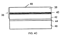
- FIGS. 4A-4D are a schematic cross sectional views illustrating steps during fabrication of a VLED structure having an n-type confinement layer with an inverted surface.
- VLED vertical light emitting diode
- steps in a method for fabricating a vertical light emitting diode (VLED) structure 32 are illustrated.
- various elements of the vertical light emitting diode (VLED) structure 32 are not illustrated in all of the figures.
- this type of vertical light emitting diode (VLED) structure is further described in U.S. Pat. No. 7,615,789, which is incorporated herein by reference.
- a carrier substrate 34 can be provided.
- the carrier substrate 34 can be in the form of a wafer comprised of a suitable material, such as sapphire, silicon carbide (SiC), silicon, germanium, zinc oxide (ZnO), or gallium arsenide (GaAs).
- a semiconductor structure 36 comprising a multi-layer epitaxial stack can be formed on the carrier substrate 34 .
- the semiconductor structure 36 can be formed using a suitable deposition process such as vapor phase epitaxy (VPE), molecular beam epitaxy (MBE) or liquid phase epitaxy (LPE).
- VPE vapor phase epitaxy
- MBE molecular beam epitaxy
- LPE liquid phase epitaxy
- the semiconductor structure 36 includes an n-type confinement layer 38 , a multiple quantum well (MQW) layer 40 on the n-type confinement layer 38 configured to emit electromagnetic radiation, and a p-type confinement layer 42 on the n-type confinement layer 38 .
- MQW multiple quantum well
- the n-type confinement layer 38 ( FIG. 4A ) preferably comprises n-GaN.
- Other suitable materials for the n-type confinement layer 38 include n-AlGaN, n-InGaN, n-AlInGaN, AlInN and n-AlN.
- the multiple quantum well (MQW) layer 40 preferably includes one or more quantum wells comprising one or more layers of InGaN/GaN, AlGaInN, AlGaN, AlInN and AlN.
- the multiple quantum well (MQW) layer 40 can be configured to emit electromagnetic radiation from the visible spectral region (e.g., 400-770 nm), the violet-indigo spectral region (e.g., 400-450 nm), the blue spectral region (e.g., 450-490 nm), the green spectral region (e.g., 490-560 nm), the yellow spectral region (e.g., 560-590 nm), the orange spectral region (e.g., 590-635 nm) or the red spectral region (e.g., 635-700 nm).
- the p-type confinement layer 42 preferably comprises p-GaN.
- Other suitable materials for the p-type confinement layer 42 include p-AlGaN, p-InGaN, p-AlInGaN, p-AlInN and p-AlN.
- a reflective layer 44 can be formed on the p-type confinement layer 42 and a thin protective layer (not shown), such as a layer of SiO 2 can be formed on the reflective layer 44 .
- the reflective layer 44 can comprise multiple layers, such as Ni/Ag/Ni/Au, Ag/Ni/Au, Ti/Ag/Ni/Au, Ag/Pt or Ag/Pd or Ag/Cr, formed by depositing an alloy containing Ag, Au, Cr, Pt, Pd, or AI.
- a thickness of the reflective layer 44 can be less than about 1.0 ⁇ m.
- High temperature annealing or alloying of the reflective layer 44 can be used to improve the contact resistance and adhesion of the reflective layer 44 to the p-type confinement layer 42 .
- the annealing or alloying process can be conducted at a temperature of at least 150° C. in an inert environment (e.g., an atmosphere containing little or no oxygen, hydrogen, or neither oxygen nor hydrogen).
- a conductive substrate 46 can be formed on the reflective layer 44 .
- the conductive substrate 46 can comprise a single metal layer or a stack of two or more metal layers, formed using a suitable deposition process.
- the material for the conductive substrate 46 can be selected to provide a high electrical conductivity and a high thermal conductivity. Suitable materials for the conductive substrate 46 include W, Ti, Mo, Al, Cu, Ni, Ag, Au, Co, Cu—Co, Ni—Co, Cu—Mo, Ni/Cu, Ni/Cu—Mo and alloys of these metals.
- Suitable deposition processes for forming the conductive substrate 46 include electro-deposition, electroless-deposition, chemical vapor deposition (CVD), plasma enhanced chemical vapor deposition (PECVD), physical vapor deposition (PVD), evaporation, and plasma spray.
- the first conductive substrate 46 can comprise a semiconductor material, such as Si, or another material, such SiO 2 , GaAs, SiC, AlN, Al 2 O 3 , or sapphire.
- a substrate removing process can be performed to separate the carrier substrate 34 from the n-type confinement layer 38 and expose an inverted surface 48 .
- the substrate removing process can be performed using a laser system 52 configured to generate a plurality of laser pulses 54 .
- the laser system 52 can comprise a conventional laser system configured to focus the laser pulses 54 at the interface of the carrier substrate 34 and the n-type confinement layer 38 .
- One suitable laser system 52 comprises a UV (266 nm) Q switching diode pump laser system.
- Another suitable laser system 52 comprises a UV excimer gas laser using ArF at 193 nm, KrF at 248 nm and F2 at 155 nm.
- the operational parameters of the laser system 52 can be selected so that the laser pulses 54 decompose the interfacial layers of the n-type confinement layer 38 with the carrier substrate 34 , permitting removal of the carrier substrate 34 .
- the laser pulses 54 can be larger than the size of the devices being fabricated, such that an overlap of two laser pulses 54 can occur such as in the middle of a street between devices.
- removal of the carrier substrate 34 using laser pulses 54 is preferred, other methods, such as chemical lift off (wet etching) or mechanical lift off (grinding, polishing, CMP), can alternately be employed.
- the semiconductor structure 36 can be flipped or rotated 180° so that the inverted surface 48 faces outward and upward.
- the n-type confinement layer 38 comprising a nitrogen containing material, such as GaN, AlGaN, InGaN, AlInGaN, AlInN and AlN
- this crystalline structure is sometimes referred to as being nitrogen-terminated, and the inverted surface is referred to a nitrogen-terminated surface.
- the n-type confinement layer 38 comprising n-GaN
- the inverted surface 48 has the crystalline structure shown in FIG. 2B .
- the atomic bonds between the N atoms 24 and the Ga atoms 22 have an inverted configuration compared to the crystalline structure shown in FIG. 2A .
- the inverted surface 48 also has different properties compared to the as-deposited GaN surface 30 shown in FIG. 2A .
- an n-contact 50 can be formed on the inverted surface 48 in electrical contact with the n-type confinement layer 38 .
- the n-contact 50 can comprise a conductive material, such as a single layer of a metal or a metal stack.
- the n-contact 50 can be formed using a suitable deposition process, such as an electro-deposition process or an electroless deposition process, to a desired thickness (e.g., 1 ⁇ m to 500 ⁇ m) and with a desired geometry.
- Suitable deposition processes for forming the n-contact 50 can include chemical vapor deposition (CVD), metal-organic chemical vapor deposition (MOCVD), plasma enhanced chemical vapor deposition (PECVD), molecular beam epitaxy (MBE), vapor phase epitaxy (VPE), physical vapor deposition (PVD), evaporation, and plasma spray.
- CVD chemical vapor deposition
- MOCVD metal-organic chemical vapor deposition
- PECVD plasma enhanced chemical vapor deposition
- MBE molecular beam epitaxy
- VPE vapor phase epitaxy
- PVD physical vapor deposition
- evaporation evaporation
- plasma spray evapor deposition
- the n-contact 50 can be formed as a stable, low resistance contact to lower the forward voltage (V F ) for obtaining high power efficiency, and better reliability in a VLED device.
- V F forward voltage
- the term “low resistance contact” generally refers to a contact having less than 5 ⁇ 10 ⁇ 2 ohm-cm 2 , preferably with less than 5 ⁇ 10 ⁇ 5 ohm-cm 2 .
- the term “stable” means a contact resistance having less than 10% variation during operation.
- the n-contact 50 can comprise an Al material such as Al/Ni/Au, AlTi/Ni/Au, Al/Pt/Au, Al/TaN/Au, AlTi/Pt/Au, AlTi/TaN/Au, AlSi/Ni/Au, AlSi/Pt,/Au, AlSiTaN/Au, AlCu/Ni/Au, AlCu/Pt/Au, and AlCu/TaN/Au.
- the n-contact 50 can comprise a low work function metal, such as Sn, Zn, Mg, Hf, W, Ta, Co, Vd, Mo and their alloys can be used.
- Suitable materials for the n-contact include Sn/Ni/Au, Sn/TaN/Au, Sn/Pt/Au, Zn/Ni/Au, Zn/TaN/Au, Zn/Pt/Au, Mg/Ni/Au, Mg/TaN/Au, Mg/Pt/Au, Hf/TaN/Au, Hf/Pt/Au, W/Au, W/Ni/Au, W/Pt/Au, Ta/Ni/Au, and Co/N/Au.
- VLED vertical light emitting diode
Abstract
Description
Claims (17)
Priority Applications (1)
| Application Number | Priority Date | Filing Date | Title |
|---|---|---|---|
| US14/176,292 US8871547B2 (en) | 2005-01-11 | 2014-02-10 | Method for fabricating vertical light emitting diode (VLED) structure using a laser pulse to remove a carrier substrate |
Applications Claiming Priority (3)
| Application Number | Priority Date | Filing Date | Title |
|---|---|---|---|
| US11/032,882 US7432119B2 (en) | 2005-01-11 | 2005-01-11 | Light emitting diode with conducting metal substrate |
| US11/761,897 US8685764B2 (en) | 2005-01-11 | 2007-06-12 | Method to make low resistance contact |
| US14/176,292 US8871547B2 (en) | 2005-01-11 | 2014-02-10 | Method for fabricating vertical light emitting diode (VLED) structure using a laser pulse to remove a carrier substrate |
Related Parent Applications (1)
| Application Number | Title | Priority Date | Filing Date |
|---|---|---|---|
| US11/761,897 Continuation-In-Part US8685764B2 (en) | 2005-01-11 | 2007-06-12 | Method to make low resistance contact |
Publications (2)
| Publication Number | Publication Date |
|---|---|
| US20140154821A1 US20140154821A1 (en) | 2014-06-05 |
| US8871547B2 true US8871547B2 (en) | 2014-10-28 |
Family
ID=50825825
Family Applications (1)
| Application Number | Title | Priority Date | Filing Date |
|---|---|---|---|
| US14/176,292 Active US8871547B2 (en) | 2005-01-11 | 2014-02-10 | Method for fabricating vertical light emitting diode (VLED) structure using a laser pulse to remove a carrier substrate |
Country Status (1)
| Country | Link |
|---|---|
| US (1) | US8871547B2 (en) |
Cited By (12)
| Publication number | Priority date | Publication date | Assignee | Title |
|---|---|---|---|---|
| US20160020120A1 (en) * | 2014-07-20 | 2016-01-21 | X-Celeprint Limited | Apparatus and methods for micro-transfer-printing |
| US9704821B2 (en) | 2015-08-11 | 2017-07-11 | X-Celeprint Limited | Stamp with structured posts |
| US10103069B2 (en) | 2016-04-01 | 2018-10-16 | X-Celeprint Limited | Pressure-activated electrical interconnection by micro-transfer printing |
| US10181483B2 (en) | 2010-03-29 | 2019-01-15 | X-Celeprint Limited | Laser assisted transfer welding process |
| US10189243B2 (en) | 2011-09-20 | 2019-01-29 | X-Celeprint Limited | Printing transferable components using microstructured elastomeric surfaces with pressure modulated reversible adhesion |
| US10222698B2 (en) | 2016-07-28 | 2019-03-05 | X-Celeprint Limited | Chiplets with wicking posts |
| US10468363B2 (en) | 2015-08-10 | 2019-11-05 | X-Celeprint Limited | Chiplets with connection posts |
| US10748793B1 (en) | 2019-02-13 | 2020-08-18 | X Display Company Technology Limited | Printing component arrays with different orientations |
| US11064609B2 (en) | 2016-08-04 | 2021-07-13 | X Display Company Technology Limited | Printable 3D electronic structure |
| US11508875B2 (en) * | 2017-12-22 | 2022-11-22 | Dowa Electronics Materials Co., Ltd. | Semiconductor light-emitting device and method of manufacturing the same |
| US11515448B2 (en) * | 2018-04-19 | 2022-11-29 | Dowa Electronics Materials Co., Ltd. | Semiconductor light-emitting element and method of manufacturing the same |
| US11637220B1 (en) | 2018-04-19 | 2023-04-25 | Dowa Electronics Materials Co., Ltd. | Semiconductor light-emitting element |
Families Citing this family (3)
| Publication number | Priority date | Publication date | Assignee | Title |
|---|---|---|---|---|
| US9653435B2 (en) | 2015-07-14 | 2017-05-16 | SemiLEDs Optoelectronics Co., Ltd. | Light emitting diode (LED) package having short circuit (VLED) die, lens support dam and same side electrodes and method of fabrication |
| US10573544B1 (en) | 2018-10-17 | 2020-02-25 | X-Celeprint Limited | Micro-transfer printing with selective component removal |
| US10796938B2 (en) * | 2018-10-17 | 2020-10-06 | X Display Company Technology Limited | Micro-transfer printing with selective component removal |
Citations (28)
| Publication number | Priority date | Publication date | Assignee | Title |
|---|---|---|---|---|
| US6071795A (en) | 1998-01-23 | 2000-06-06 | The Regents Of The University Of California | Separation of thin films from transparent substrates by selective optical processing |
| US6172382B1 (en) * | 1997-01-09 | 2001-01-09 | Nichia Chemical Industries, Ltd. | Nitride semiconductor light-emitting and light-receiving devices |
| US6221683B1 (en) | 1997-05-27 | 2001-04-24 | Osram Opto Semiconductor Gmbh & Co. Ohg | Method for producing a light-emitting component |
| US6365429B1 (en) | 1998-12-30 | 2002-04-02 | Xerox Corporation | Method for nitride based laser diode with growth substrate removed using an intermediate substrate |
| US6455877B1 (en) * | 1999-09-08 | 2002-09-24 | Sharp Kabushiki Kaisha | III-N compound semiconductor device |
| US6555405B2 (en) | 2001-03-22 | 2003-04-29 | Uni Light Technology, Inc. | Method for forming a semiconductor device having a metal substrate |
| US6658041B2 (en) | 2002-03-20 | 2003-12-02 | Agilent Technologies, Inc. | Wafer bonded vertical cavity surface emitting laser systems |
| US6744071B2 (en) | 2002-01-28 | 2004-06-01 | Nichia Corporation | Nitride semiconductor element with a supporting substrate |
| US6746889B1 (en) | 2001-03-27 | 2004-06-08 | Emcore Corporation | Optoelectronic device with improved light extraction |
| US20040135158A1 (en) | 2003-01-03 | 2004-07-15 | Supernova Optoelectronics Corp. | Method for manufacturing of a vertical light emitting device structure |
| US6770542B2 (en) | 2001-12-20 | 2004-08-03 | Osram Opto Semiconductors Gmbh | Method for fabricating semiconductor layers |
| US20040166599A1 (en) | 2000-02-10 | 2004-08-26 | Sharp Kabushiki Kaisha | Semiconductor light emitting device and method for producing the same |
| US6800500B2 (en) | 1999-02-05 | 2004-10-05 | Lumileds Lighting U.S., Llc | III-nitride light emitting devices fabricated by substrate removal |
| US20040209402A1 (en) | 2003-03-18 | 2004-10-21 | Crystal Photonics, Incorporated | Method for making Group III nitride devices and devices produced thereby |
| US20040245543A1 (en) | 2003-06-04 | 2004-12-09 | Yoo Myung Cheol | Method of fabricating vertical structure compound semiconductor devices |
| US20050098792A1 (en) | 2002-04-09 | 2005-05-12 | Jong-Lam Lee | Method of fabricating vertical structure LEDs |
| US20050196888A1 (en) | 1998-06-26 | 2005-09-08 | Sony Corporation | Method of crystallizing a nitride III-V compound semiconductor layer on a sapphire substrate |
| US20060154391A1 (en) | 2005-01-11 | 2006-07-13 | Tran Chuong A | Light emitting diodes (LEDs) with improved light extraction by roughening |
| US20060154392A1 (en) | 2005-01-11 | 2006-07-13 | Tran Chuong A | Method of making a vertical light emitting diode |
| US20060154390A1 (en) | 2005-01-11 | 2006-07-13 | Tran Chuong A | Systems and methods for producing light emitting diode array |
| US20060154393A1 (en) | 2005-01-11 | 2006-07-13 | Doan Trung T | Systems and methods for removing operating heat from a light emitting diode |
| US20060157721A1 (en) | 2005-01-11 | 2006-07-20 | Tran Chuong A | Systems and methods for producing white-light light emitting diodes |
| US20070121690A1 (en) * | 2003-12-09 | 2007-05-31 | Tetsuo Fujii | Highly efficient gallium nitride based light emitting diodes via surface roughening |
| US20080035950A1 (en) | 2005-01-11 | 2008-02-14 | Chen-Fu Chu | Method to make low resistance contact |
| US7432119B2 (en) | 2005-01-11 | 2008-10-07 | Semileds Corporation | Light emitting diode with conducting metal substrate |
| US7432882B2 (en) | 2003-07-15 | 2008-10-07 | Hitachi, Ltd. | Driving circuit for plasma display panel using offset waveform |
| US7615789B2 (en) | 2006-05-09 | 2009-11-10 | SemiLEDs Optoelectronics Co., Ltd. | Vertical light emitting diode device structure |
| US8507302B1 (en) | 2005-10-11 | 2013-08-13 | SemiLEDs Optoelectronics Co., Ltd. | Wall structures for a semiconductor wafer |
-
2014
- 2014-02-10 US US14/176,292 patent/US8871547B2/en active Active
Patent Citations (31)
| Publication number | Priority date | Publication date | Assignee | Title |
|---|---|---|---|---|
| US6172382B1 (en) * | 1997-01-09 | 2001-01-09 | Nichia Chemical Industries, Ltd. | Nitride semiconductor light-emitting and light-receiving devices |
| US6221683B1 (en) | 1997-05-27 | 2001-04-24 | Osram Opto Semiconductor Gmbh & Co. Ohg | Method for producing a light-emitting component |
| US6071795A (en) | 1998-01-23 | 2000-06-06 | The Regents Of The University Of California | Separation of thin films from transparent substrates by selective optical processing |
| US20050196888A1 (en) | 1998-06-26 | 2005-09-08 | Sony Corporation | Method of crystallizing a nitride III-V compound semiconductor layer on a sapphire substrate |
| US6365429B1 (en) | 1998-12-30 | 2002-04-02 | Xerox Corporation | Method for nitride based laser diode with growth substrate removed using an intermediate substrate |
| US6448102B1 (en) | 1998-12-30 | 2002-09-10 | Xerox Corporation | Method for nitride based laser diode with growth substrate removed |
| US6800500B2 (en) | 1999-02-05 | 2004-10-05 | Lumileds Lighting U.S., Llc | III-nitride light emitting devices fabricated by substrate removal |
| US6455877B1 (en) * | 1999-09-08 | 2002-09-24 | Sharp Kabushiki Kaisha | III-N compound semiconductor device |
| US20040166599A1 (en) | 2000-02-10 | 2004-08-26 | Sharp Kabushiki Kaisha | Semiconductor light emitting device and method for producing the same |
| US6555405B2 (en) | 2001-03-22 | 2003-04-29 | Uni Light Technology, Inc. | Method for forming a semiconductor device having a metal substrate |
| US6746889B1 (en) | 2001-03-27 | 2004-06-08 | Emcore Corporation | Optoelectronic device with improved light extraction |
| US6770542B2 (en) | 2001-12-20 | 2004-08-03 | Osram Opto Semiconductors Gmbh | Method for fabricating semiconductor layers |
| US6744071B2 (en) | 2002-01-28 | 2004-06-01 | Nichia Corporation | Nitride semiconductor element with a supporting substrate |
| US6658041B2 (en) | 2002-03-20 | 2003-12-02 | Agilent Technologies, Inc. | Wafer bonded vertical cavity surface emitting laser systems |
| US20060099730A1 (en) | 2002-04-09 | 2006-05-11 | Lg Electronics Inc. | Method of fabricating vertical structure LEDs |
| US20050098792A1 (en) | 2002-04-09 | 2005-05-12 | Jong-Lam Lee | Method of fabricating vertical structure LEDs |
| US20040135158A1 (en) | 2003-01-03 | 2004-07-15 | Supernova Optoelectronics Corp. | Method for manufacturing of a vertical light emitting device structure |
| US20040209402A1 (en) | 2003-03-18 | 2004-10-21 | Crystal Photonics, Incorporated | Method for making Group III nitride devices and devices produced thereby |
| US20040245543A1 (en) | 2003-06-04 | 2004-12-09 | Yoo Myung Cheol | Method of fabricating vertical structure compound semiconductor devices |
| US7432882B2 (en) | 2003-07-15 | 2008-10-07 | Hitachi, Ltd. | Driving circuit for plasma display panel using offset waveform |
| US20070121690A1 (en) * | 2003-12-09 | 2007-05-31 | Tetsuo Fujii | Highly efficient gallium nitride based light emitting diodes via surface roughening |
| US20060154390A1 (en) | 2005-01-11 | 2006-07-13 | Tran Chuong A | Systems and methods for producing light emitting diode array |
| US20060154393A1 (en) | 2005-01-11 | 2006-07-13 | Doan Trung T | Systems and methods for removing operating heat from a light emitting diode |
| US20060157721A1 (en) | 2005-01-11 | 2006-07-20 | Tran Chuong A | Systems and methods for producing white-light light emitting diodes |
| US20060154392A1 (en) | 2005-01-11 | 2006-07-13 | Tran Chuong A | Method of making a vertical light emitting diode |
| US20080035950A1 (en) | 2005-01-11 | 2008-02-14 | Chen-Fu Chu | Method to make low resistance contact |
| US7432119B2 (en) | 2005-01-11 | 2008-10-07 | Semileds Corporation | Light emitting diode with conducting metal substrate |
| US20060154391A1 (en) | 2005-01-11 | 2006-07-13 | Tran Chuong A | Light emitting diodes (LEDs) with improved light extraction by roughening |
| US8685764B2 (en) | 2005-01-11 | 2014-04-01 | SemiLEDs Optoelectronics Co., Ltd. | Method to make low resistance contact |
| US8507302B1 (en) | 2005-10-11 | 2013-08-13 | SemiLEDs Optoelectronics Co., Ltd. | Wall structures for a semiconductor wafer |
| US7615789B2 (en) | 2006-05-09 | 2009-11-10 | SemiLEDs Optoelectronics Co., Ltd. | Vertical light emitting diode device structure |
Non-Patent Citations (6)
| Title |
|---|
| Final Office Action from U.S. Appl. No. 11/761,897 dated Aug. 31, 2009, pp. 1-7. |
| Final Office Action from U.S. Appl. No. 11/761,897 dated Oct. 31, 2008, pp. 1-7. |
| Non-Final Office Action from U.S. Appl. No. 11/761,897 dated Feb. 18, 2009, pp. 1-7. |
| Non-Final Office Action from U.S. Appl. No. 11/761,897 dated Mar. 12, 2008, pp. 1-7. |
| Notice of Allowance from U.S. Appl. No. 11/761,897 dated Nov. 12, 2013, pp. 1-7. |
| PCT International Search Report and Written Opinion dated Dec. 23, 2009 for PCT Application No. PCT/US08/66378, pp. 1-10. |
Cited By (22)
| Publication number | Priority date | Publication date | Assignee | Title |
|---|---|---|---|---|
| US10181483B2 (en) | 2010-03-29 | 2019-01-15 | X-Celeprint Limited | Laser assisted transfer welding process |
| US10717267B2 (en) | 2011-09-20 | 2020-07-21 | X Display Company Technology Limited | Printing transferable components using microstructured elastomeric surfaces with pressure modulated reversible adhesion |
| US10189243B2 (en) | 2011-09-20 | 2019-01-29 | X-Celeprint Limited | Printing transferable components using microstructured elastomeric surfaces with pressure modulated reversible adhesion |
| US11472171B2 (en) | 2014-07-20 | 2022-10-18 | X Display Company Technology Limited | Apparatus and methods for micro-transfer-printing |
| US9434150B2 (en) * | 2014-07-20 | 2016-09-06 | X-Celeprint Limited | Apparatus and methods for micro-transfer-printing |
| US10252514B2 (en) | 2014-07-20 | 2019-04-09 | X-Celeprint Limited | Apparatus and methods for micro-transfer-printing |
| US20160020120A1 (en) * | 2014-07-20 | 2016-01-21 | X-Celeprint Limited | Apparatus and methods for micro-transfer-printing |
| US10899067B2 (en) | 2015-07-20 | 2021-01-26 | X Display Company Technology Limited | Multi-layer stamp |
| US11276657B2 (en) | 2015-08-10 | 2022-03-15 | X Display Company Technology Limited | Chiplets with connection posts |
| US11552034B2 (en) | 2015-08-10 | 2023-01-10 | X Display Company Technology Limited | Chiplets with connection posts |
| US10468363B2 (en) | 2015-08-10 | 2019-11-05 | X-Celeprint Limited | Chiplets with connection posts |
| US10777521B2 (en) | 2015-08-10 | 2020-09-15 | X Display Company Technology Limited | Printable component structure with electrical contact |
| US9704821B2 (en) | 2015-08-11 | 2017-07-11 | X-Celeprint Limited | Stamp with structured posts |
| US11318663B2 (en) | 2015-10-20 | 2022-05-03 | X Display Company Technology Limited | Multi-layer stamp |
| US10163735B2 (en) | 2016-04-01 | 2018-12-25 | X-Celeprint Limited | Pressure-activated electrical interconnection by micro-transfer printing |
| US10103069B2 (en) | 2016-04-01 | 2018-10-16 | X-Celeprint Limited | Pressure-activated electrical interconnection by micro-transfer printing |
| US10222698B2 (en) | 2016-07-28 | 2019-03-05 | X-Celeprint Limited | Chiplets with wicking posts |
| US11064609B2 (en) | 2016-08-04 | 2021-07-13 | X Display Company Technology Limited | Printable 3D electronic structure |
| US11508875B2 (en) * | 2017-12-22 | 2022-11-22 | Dowa Electronics Materials Co., Ltd. | Semiconductor light-emitting device and method of manufacturing the same |
| US11637220B1 (en) | 2018-04-19 | 2023-04-25 | Dowa Electronics Materials Co., Ltd. | Semiconductor light-emitting element |
| US11515448B2 (en) * | 2018-04-19 | 2022-11-29 | Dowa Electronics Materials Co., Ltd. | Semiconductor light-emitting element and method of manufacturing the same |
| US10748793B1 (en) | 2019-02-13 | 2020-08-18 | X Display Company Technology Limited | Printing component arrays with different orientations |
Also Published As
| Publication number | Publication date |
|---|---|
| US20140154821A1 (en) | 2014-06-05 |
Similar Documents
| Publication | Publication Date | Title |
|---|---|---|
| US8871547B2 (en) | Method for fabricating vertical light emitting diode (VLED) structure using a laser pulse to remove a carrier substrate | |
| JP5278317B2 (en) | Manufacturing method of light emitting diode | |
| EP1810351B1 (en) | Gan compound semiconductor light emitting element | |
| US11211537B2 (en) | Vertical light emitting devices with nickel silicide bonding and methods of manufacturing | |
| US7432119B2 (en) | Light emitting diode with conducting metal substrate | |
| US7723718B1 (en) | Epitaxial structure for metal devices | |
| US8685764B2 (en) | Method to make low resistance contact | |
| US7892891B2 (en) | Die separation | |
| US11335830B2 (en) | Photo-emission semiconductor device and method of manufacturing same | |
| US20120034718A1 (en) | Vertical deep ultraviolet light emitting diodes | |
| EP1793429A1 (en) | Semiconductor light emitting device having a reflection layer comprising silver | |
| US9437794B2 (en) | Method of fabricating a flip chip light emitting diode (FCLED) die having N-conductor layer | |
| US20110266575A1 (en) | Nitride-based semiconductor device and method for fabricating the same | |
| WO2003023838A1 (en) | n ELECTRODE FOR III GROUP NITRIDE BASED COMPOUND SEMICONDUCTOR ELEMENT | |
| US8778780B1 (en) | Method for defining semiconductor devices | |
| KR20100036760A (en) | Light emitting diode and method for fabricating the same |
Legal Events
| Date | Code | Title | Description |
|---|---|---|---|
| FEPP | Fee payment procedure |
Free format text: PAYOR NUMBER ASSIGNED (ORIGINAL EVENT CODE: ASPN); ENTITY STATUS OF PATENT OWNER: SMALL ENTITY |
|
| AS | Assignment |
Owner name: SEMILEDS OPTOELECTRONICS CO. LTD., TAIWAN Free format text: ASSIGNMENT OF ASSIGNORS INTEREST;ASSIGNORS:CHU, CHEN-FU;LIU, WEN-HUANG;CHENG, HAO-CHUN;AND OTHERS;SIGNING DATES FROM 20140206 TO 20140207;REEL/FRAME:032226/0733 |
|
| STCF | Information on status: patent grant |
Free format text: PATENTED CASE |
|
| MAFP | Maintenance fee payment |
Free format text: PAYMENT OF MAINTENANCE FEE, 4TH YR, SMALL ENTITY (ORIGINAL EVENT CODE: M2551) Year of fee payment: 4 |
|
| MAFP | Maintenance fee payment |
Free format text: PAYMENT OF MAINTENANCE FEE, 8TH YR, SMALL ENTITY (ORIGINAL EVENT CODE: M2552); ENTITY STATUS OF PATENT OWNER: SMALL ENTITY Year of fee payment: 8 |