US8882983B2 - Embedded thin films - Google Patents

Embedded thin films Download PDF

Info

Publication number
US8882983B2
US8882983B2 US12/482,202 US48220209A US8882983B2 US 8882983 B2 US8882983 B2 US 8882983B2 US 48220209 A US48220209 A US 48220209A US 8882983 B2 US8882983 B2 US 8882983B2
Authority
US
United States
Prior art keywords
solution
ceramic film
film
conductive surface
conductive
Prior art date
Legal status (The legal status is an assumption and is not a legal conclusion. Google has not performed a legal analysis and makes no representation as to the accuracy of the status listed.)
Expired - Fee Related, expires
Application number
US12/482,202
Other versions
US20090301770A1 (en
Inventor
Junghyun Cho
Bahgat Sammakia
Mark D. Poliks
Roy Magnuson
Biplab Kumar Roy
Current Assignee (The listed assignees may be inaccurate. Google has not performed a legal analysis and makes no representation or warranty as to the accuracy of the list.)
Research Foundation of State University of New York
Original Assignee
Research Foundation of State University of New York
Priority date (The priority date is an assumption and is not a legal conclusion. Google has not performed a legal analysis and makes no representation as to the accuracy of the date listed.)
Filing date
Publication date
Application filed by Research Foundation of State University of New York filed Critical Research Foundation of State University of New York
Priority to US12/482,202 priority Critical patent/US8882983B2/en
Publication of US20090301770A1 publication Critical patent/US20090301770A1/en
Assigned to THE RESEARCH FOUNDATION FOR THE STATE UNIVERSITY OF NEW YORK reassignment THE RESEARCH FOUNDATION FOR THE STATE UNIVERSITY OF NEW YORK CHANGE OF NAME (SEE DOCUMENT FOR DETAILS). Assignors: THE RESEARCH FOUNDATION OF STATE UNIVERSITY OF NEW YORK
Assigned to THE RESEARCH FOUNDATION OF STATE UNIVERSITY OF NEW YORK reassignment THE RESEARCH FOUNDATION OF STATE UNIVERSITY OF NEW YORK ASSIGNMENT OF ASSIGNORS INTEREST (SEE DOCUMENT FOR DETAILS). Assignors: CHO, JUNGHYUN, ROY, BIPLAB KUMAR, SAMMAKIA, BAHGAT
Priority to US14/537,123 priority patent/US10064283B2/en
Application granted granted Critical
Publication of US8882983B2 publication Critical patent/US8882983B2/en
Expired - Fee Related legal-status Critical Current
Adjusted expiration legal-status Critical

Links

Images

Classifications

    • HELECTRICITY
    • H05ELECTRIC TECHNIQUES NOT OTHERWISE PROVIDED FOR
    • H05KPRINTED CIRCUITS; CASINGS OR CONSTRUCTIONAL DETAILS OF ELECTRIC APPARATUS; MANUFACTURE OF ASSEMBLAGES OF ELECTRICAL COMPONENTS
    • H05K3/00Apparatus or processes for manufacturing printed circuits
    • H05K3/0011Working of insulating substrates or insulating layers
    • CCHEMISTRY; METALLURGY
    • C25ELECTROLYTIC OR ELECTROPHORETIC PROCESSES; APPARATUS THEREFOR
    • C25DPROCESSES FOR THE ELECTROLYTIC OR ELECTROPHORETIC PRODUCTION OF COATINGS; ELECTROFORMING; APPARATUS THEREFOR
    • C25D5/00Electroplating characterised by the process; Pretreatment or after-treatment of workpieces
    • C25D5/48After-treatment of electroplated surfaces
    • CCHEMISTRY; METALLURGY
    • C25ELECTROLYTIC OR ELECTROPHORETIC PROCESSES; APPARATUS THEREFOR
    • C25DPROCESSES FOR THE ELECTROLYTIC OR ELECTROPHORETIC PRODUCTION OF COATINGS; ELECTROFORMING; APPARATUS THEREFOR
    • C25D21/00Processes for servicing or operating cells for electrolytic coating
    • C25D21/12Process control or regulation
    • CCHEMISTRY; METALLURGY
    • C25ELECTROLYTIC OR ELECTROPHORETIC PROCESSES; APPARATUS THEREFOR
    • C25DPROCESSES FOR THE ELECTROLYTIC OR ELECTROPHORETIC PRODUCTION OF COATINGS; ELECTROFORMING; APPARATUS THEREFOR
    • C25D9/00Electrolytic coating other than with metals
    • C25D9/04Electrolytic coating other than with metals with inorganic materials
    • C25D9/08Electrolytic coating other than with metals with inorganic materials by cathodic processes
    • HELECTRICITY
    • H05ELECTRIC TECHNIQUES NOT OTHERWISE PROVIDED FOR
    • H05KPRINTED CIRCUITS; CASINGS OR CONSTRUCTIONAL DETAILS OF ELECTRIC APPARATUS; MANUFACTURE OF ASSEMBLAGES OF ELECTRICAL COMPONENTS
    • H05K1/00Printed circuits
    • H05K1/02Details
    • H05K1/03Use of materials for the substrate
    • H05K1/0306Inorganic insulating substrates, e.g. ceramic, glass
    • HELECTRICITY
    • H05ELECTRIC TECHNIQUES NOT OTHERWISE PROVIDED FOR
    • H05KPRINTED CIRCUITS; CASINGS OR CONSTRUCTIONAL DETAILS OF ELECTRIC APPARATUS; MANUFACTURE OF ASSEMBLAGES OF ELECTRICAL COMPONENTS
    • H05K1/00Printed circuits
    • H05K1/02Details
    • H05K1/09Use of materials for the conductive, e.g. metallic pattern
    • HELECTRICITY
    • H05ELECTRIC TECHNIQUES NOT OTHERWISE PROVIDED FOR
    • H05KPRINTED CIRCUITS; CASINGS OR CONSTRUCTIONAL DETAILS OF ELECTRIC APPARATUS; MANUFACTURE OF ASSEMBLAGES OF ELECTRICAL COMPONENTS
    • H05K1/00Printed circuits
    • H05K1/16Printed circuits incorporating printed electric components, e.g. printed resistor, capacitor, inductor
    • H05K1/162Printed circuits incorporating printed electric components, e.g. printed resistor, capacitor, inductor incorporating printed capacitors
    • HELECTRICITY
    • H05ELECTRIC TECHNIQUES NOT OTHERWISE PROVIDED FOR
    • H05KPRINTED CIRCUITS; CASINGS OR CONSTRUCTIONAL DETAILS OF ELECTRIC APPARATUS; MANUFACTURE OF ASSEMBLAGES OF ELECTRICAL COMPONENTS
    • H05K1/00Printed circuits
    • H05K1/16Printed circuits incorporating printed electric components, e.g. printed resistor, capacitor, inductor
    • H05K1/167Printed circuits incorporating printed electric components, e.g. printed resistor, capacitor, inductor incorporating printed resistors
    • HELECTRICITY
    • H05ELECTRIC TECHNIQUES NOT OTHERWISE PROVIDED FOR
    • H05KPRINTED CIRCUITS; CASINGS OR CONSTRUCTIONAL DETAILS OF ELECTRIC APPARATUS; MANUFACTURE OF ASSEMBLAGES OF ELECTRICAL COMPONENTS
    • H05K2201/00Indexing scheme relating to printed circuits covered by H05K1/00
    • H05K2201/01Dielectrics
    • H05K2201/0137Materials
    • H05K2201/0175Inorganic, non-metallic layer, e.g. resist or dielectric for printed capacitor
    • HELECTRICITY
    • H05ELECTRIC TECHNIQUES NOT OTHERWISE PROVIDED FOR
    • H05KPRINTED CIRCUITS; CASINGS OR CONSTRUCTIONAL DETAILS OF ELECTRIC APPARATUS; MANUFACTURE OF ASSEMBLAGES OF ELECTRICAL COMPONENTS
    • H05K2201/00Indexing scheme relating to printed circuits covered by H05K1/00
    • H05K2201/03Conductive materials
    • H05K2201/0332Structure of the conductor
    • H05K2201/0335Layered conductors or foils
    • H05K2201/0355Metal foils
    • HELECTRICITY
    • H05ELECTRIC TECHNIQUES NOT OTHERWISE PROVIDED FOR
    • H05KPRINTED CIRCUITS; CASINGS OR CONSTRUCTIONAL DETAILS OF ELECTRIC APPARATUS; MANUFACTURE OF ASSEMBLAGES OF ELECTRICAL COMPONENTS
    • H05K2203/00Indexing scheme relating to apparatus or processes for manufacturing printed circuits covered by H05K3/00
    • H05K2203/09Treatments involving charged particles
    • H05K2203/092Particle beam, e.g. using an electron beam or an ion beam
    • HELECTRICITY
    • H05ELECTRIC TECHNIQUES NOT OTHERWISE PROVIDED FOR
    • H05KPRINTED CIRCUITS; CASINGS OR CONSTRUCTIONAL DETAILS OF ELECTRIC APPARATUS; MANUFACTURE OF ASSEMBLAGES OF ELECTRICAL COMPONENTS
    • H05K2203/00Indexing scheme relating to apparatus or processes for manufacturing printed circuits covered by H05K3/00
    • H05K2203/13Moulding and encapsulation; Deposition techniques; Protective layers
    • H05K2203/1333Deposition techniques, e.g. coating
    • H05K2203/135Electrophoretic deposition of insulating material
    • HELECTRICITY
    • H05ELECTRIC TECHNIQUES NOT OTHERWISE PROVIDED FOR
    • H05KPRINTED CIRCUITS; CASINGS OR CONSTRUCTIONAL DETAILS OF ELECTRIC APPARATUS; MANUFACTURE OF ASSEMBLAGES OF ELECTRICAL COMPONENTS
    • H05K2203/00Indexing scheme relating to apparatus or processes for manufacturing printed circuits covered by H05K3/00
    • H05K2203/16Inspection; Monitoring; Aligning
    • H05K2203/163Monitoring a manufacturing process
    • HELECTRICITY
    • H05ELECTRIC TECHNIQUES NOT OTHERWISE PROVIDED FOR
    • H05KPRINTED CIRCUITS; CASINGS OR CONSTRUCTIONAL DETAILS OF ELECTRIC APPARATUS; MANUFACTURE OF ASSEMBLAGES OF ELECTRICAL COMPONENTS
    • H05K3/00Apparatus or processes for manufacturing printed circuits
    • H05K3/10Apparatus or processes for manufacturing printed circuits in which conductive material is applied to the insulating support in such a manner as to form the desired conductive pattern
    • H05K3/18Apparatus or processes for manufacturing printed circuits in which conductive material is applied to the insulating support in such a manner as to form the desired conductive pattern using precipitation techniques to apply the conductive material
    • H05K3/181Apparatus or processes for manufacturing printed circuits in which conductive material is applied to the insulating support in such a manner as to form the desired conductive pattern using precipitation techniques to apply the conductive material by electroless plating
    • H05K3/182Apparatus or processes for manufacturing printed circuits in which conductive material is applied to the insulating support in such a manner as to form the desired conductive pattern using precipitation techniques to apply the conductive material by electroless plating characterised by the patterning method
    • H05K3/184Apparatus or processes for manufacturing printed circuits in which conductive material is applied to the insulating support in such a manner as to form the desired conductive pattern using precipitation techniques to apply the conductive material by electroless plating characterised by the patterning method using masks

Definitions

  • the present invention relates, in general, to systems and methods for forming thin film structures on conductive surfaces, for example, printed circuit boards (PCBs), microelectromechanical (MEM) devices, sensors, and other structures.
  • PCBs printed circuit boards
  • MEM microelectromechanical
  • PCB printed circuit boards
  • a technology for fabricating the PCBs including the passive components embedded therein achieves substitution of conventional chip resistors or chip capacitors by mounting the passive components, such as the resistors or capacitors, on an external surface of a PCB or in an internal layer of the PCB according to a process employing a formed dielectric or resistive material, such as a ceramic, carbon, or metal oxide powder, which may be mixed into an epoxy paste.
  • a formed dielectric or resistive material such as a ceramic, carbon, or metal oxide powder
  • a first method of fabricating a polymer thick film type of circuit elements applies a filled polymer paste, which is then thermally hardened (dried or cured) to fabricate a device.
  • a filled polymer paste which is then thermally hardened (dried or cured) to fabricate a device.
  • the filled device typically a capacitor
  • a copper paste is printed on the resulting PCB and dried so that electrodes are formed, thereby making an embedded device.
  • a second method is to apply a filled photosensitive resin on a PCB to fabricate a discrete type of device.
  • the photosensitive resin which contains a filler powder is applied on the printed circuit board (PCB), and a copper foil is laminated on the resulting PCB to form upper and lower electrodes, a circuit pattern is formed, and the photosensitive resin is etched to fabricate the discrete type of device.
  • a third method provides an electrochemically deposited film or film precursor layer on a substrate, typically a copper trace or pad, to form a functional film thereon, typically a dielectric layer of a capacitor.
  • the electrochemical process is associated with a corrosive and hostile environment to the underlying conductor, e.g., copper, leading to suboptimal properties of the resulting device.
  • the environment during the deposition or a post-deposition conversion process may be oxidizing, resulting in corrosion of the copper or other metal and reaction with solutes, and hydrolysis of the aqueous solvent and generation of hydrogen, resulting in embrittlement of the metal and/or separation of the conductor from its substrate.
  • the hydrolysis also results in energy inefficiency.
  • an electrochemical process leads to a protective coating which is non-conductive, and is thus self-limiting with respect to the conduct of an electrochemical process through the coating. Therefore, such processes are typically limited to thin protecting coatings (e.g., an anodization process to produce a protective oxide). Formation of coatings of arbitrary thickness is difficult, and the coatings may have properties which are limited by the process conditions, and not as an independently controlled factor over a range of thicknesses.
  • the present systems and methods provide an electrochemical process for coating a conductive surface with a ceramic or insoluble or low solubility metal salt.
  • This coating may be porous, and therefore formed with a range of thickness. The process reduces hydrolytic generation of hydrogen while avoiding corrosive conditions at the cathode.
  • ceramic thin films of high capacitance (i.e., high dielectric strength) materials are embedded within the inner layers of electronic packages or circuit boards and replace the need for placement and assembly operations of discrete surface mounted components.
  • the ceramic films have the following advantages over existing ceramic-filled epoxy or ceramic paste dielectrics or conductors:
  • the ceramic films are nanostructured and preferably have a well controlled resistivity and well controlled dimensions, while still withstanding high voltages, e.g., >15 volts, to provide appropriate characteristics.
  • a preferred embodiment provides a three-ply (tri-layer) system consisting of a top copper layer (thin film), an intermediate dielectric, conductor or semiconductor, and a bottom copper layer (foil), which is formed by a process as shown in FIG. 1 .
  • TiO 2 or BaTiO 3 are preferably used as a dielectric layer.
  • a resistor should have low capacitance, and therefore the material is selected as appropriate.
  • zinc oxide, indium oxide and tin oxide are both known resistor materials.
  • oxides are preferred; however, other chemistries for dielectrics, conductors or semiconductors may be employed with appropriate modification of the process.
  • the copper foil is typically electrochemically treated to have an extremely smooth surface to accommodate a device layer. However, in some cases, it may be microstructured to increase surface area, and thus, for example, provide a resulting device with increased capacitance.
  • Formation of ceramic thin films on the surface of copper foil may be enhanced through use of a “biomimetic” process.
  • Formation of the ceramic thin films may, for example, be aided by organic self-assembled molecules (SAM) (for example, C 12 H 29 O 6 PSi) that are primed on the copper foil which is formed on a substrate.
  • SAM organic self-assembled molecules
  • the SAM layer is not required to produce functioning capacitors or resistors.
  • the SAM layer may be employed to control or alter a crystalline property or state of the layer formed above.
  • the preferred resultant microstructure in the case of a thin film capacitor consists of 5-10 nm nanocrystallites assembled into a uniform film that are all connected via a very strong attractive force, without need for further densification, due to their small sizes.
  • the thickness of the dielectric layer can be a range of submicron to a few microns.
  • This unique thin microstructure is a basis of high dielectric constant due to continuous dielectric paths while the resultant high interfacial areas, and the nanoporosities provide a means of withstanding a large electric field without breakdown.
  • the thicknesses as well as the amount/size of porosities may be controlled to achieve the optimum dielectric constant and strength. This offers the possibility of embedded capacitors with tunable dielectric properties.
  • a relatively thick film may be desired to achieve an appropriate resistance, voltage and power handling capability.
  • the film need not be homogeneous, and may, for example, be layered during deposition, or modified after initial deposition of a precursor layer.
  • the film is typically an oxide or relatively insoluble (in water) salt of a metal, though the technique is not so limited, and may, for example, be used with respect to organic conductors and materials.
  • the substrate need not be copper, and may be any surface which is sufficiently conductive to permit the electrochemical processing.
  • the electrodes of a device may be formed from carbon nanotubes (CNT) or other conductive nanofibers, organic conductors or semiconductors, or the like. The process conducts the film forming process under conditions which sufficiently alter the microenvironment of the electrode to avoid undesired corrosion or other effects.
  • the electrochemical potential of the surface and local pH are maintained within a desired range, by, for example, applying a voltage potential to the conductive surface with respect to a reference electrode, and using a pH control for the bulk solution which achieves a desired pH, during processing, in proximity to the surface.
  • a pH control for the bulk solution which achieves a desired pH, during processing, in proximity to the surface.
  • the control of the pH may be determined empirically, or through careful measurements proximate to the surface.
  • SAM-assisted dielectric film formation permits patterning of the resulting dielectric films, since the film formation would selectively occur on the areas that have specific SAM functional groups.
  • SAM may also be useful for forming resistive films.
  • the high degree of surface selectivity afforded by this functionalization can be achieved via e-beam photolithography, ion-beam photolithography, soft pad transfer lithography, ink jet lithography or the like. (B. C. Bunker et al., Science, 264, 48 (1994).
  • the scanning probe approach can provide an alternate way for the dielectric film patterning.
  • the SAM terminus is destroyed (desorbed), replaced, or reacted on direct contact with the AFM tip, thereby producing a binary pattern of treated and untreated SAM surfaces.
  • the process may be applied, for example, to embed dielectric films standard copper plated epoxy circuit boards, and may also be used to process polyimide substrate flexible circuit boards. Such films may be used, for example, as power supply decoupling capacitors, in transmission line termination circuits, in antennas and other controlled impedance devices and transmission lines, and as embedded sensors.
  • a titania based ceramic dielectric may be formed in an ionic solution of titanium chloride (TiCl 4 ).
  • TiCl 4 titanium chloride
  • this solution is normally corrosive to the underlying copper electrode on which the dielectric is to be formed.
  • titania (TiO 2 ) films may be formed on commercial copper/FR4/copper laminates.
  • a corresponding process may be used to deposit a resistor material on the copper electrode, though typically, the salts will be different.
  • various dopants or impurities may be added to the solution (or provided in a secondary transformation process) in order to achieve a film with the desired electrical properties, for example, to provide a thermistor or embedded positive coefficient thermal element to provide switching or adaptive current distribution.
  • the film produced may have optical properties of interest.
  • titanium oxide is photohydrolytically active, and when moist and subject to sufficient illumination, will produce hydrogen and oxygen, or oxidize various chemical species in the environment, for example organic substances. Therefore, if the titania film produced by a deposition process is left uncovered, or it covered with an optically transmissive (at the wavelengths of interest) layer, then it may be used hydrolyze water or oxidize materials when illuminated.
  • a conductive electrode is present under the film, the structure may advantageously be used as a sensor, based, for example, on an electrical voltage or current produced by the structure, either without a bias voltage, or with respect to a reference electrode.
  • a cyclic voltimetry sensor may be implemented, in which the reference voltage varies over time.
  • the titania film may be chemically doped with selected impurities, and/or with particles that are incorporated into the macroscopic film. Titania also has antimicrobial properties under ultraviolet light.
  • a light source may be provided in or nearby the film.
  • an organic light emitting diode structure may be formed near the film, and also placed on or embedded in a circuit board or interconnect system.
  • a normal light emitting diode may also be mounted in proximity.
  • the film may also be illuminated by sunlight or external artificial light.
  • a light pipe structure such as a fiber optic or optically transmissive layer integrated within the system, may convey a remote light source to the film.
  • Titania may also form part of an oxygen sensor, catalytic sensor, or act as catalyst for a chemical reaction.
  • One way to avoid the corrosion of the copper substrate by the hydrogen chloride formed by reaction of TiCl 4 with water in solution is to maintain an electrochemical potential of the copper at a level which prevents oxidation of the copper, for example, negative 5V, with respect to a reference in the solution.
  • the copper film is this thus the cathode.
  • an aqueous solution subject to this potential leads to hydrolysis, which both wastes energy and leads to evolution of hydrogen at the cathode, which may damage the metallic film and hinders formation of the ceramic layer.
  • water is reduced to H 2 at the cathode, OH ⁇ ions are formed, and the pH near the cathode consequently increases.
  • H 2 O 2 hydrogen peroxide
  • Ti 4+ ions in the solution.
  • These complexes are attracted towards the cathode by the applied voltage, and due to the high pH, get converted to TiO 2 particles which are deposited onto the cathode. While the details may differ, other polyvalent metal ions may be subject to similar reactions.
  • the anode is subject to low pH.
  • the anode generally does not form part of the end product, and thus the low pH conditions are acceptable and can be tolerated.
  • the anode may be a corrosion resistant platinum electrode substantially displaced from the cathode, though other structures and materials may be used. This reaction generally proceeds at room temperature, and in any case elevated temperatures (e.g., >100° C.) are not generally required.
  • the underlying cathode electrode film, which forms part of the end product structure is cathodically protected from action of a potentially corrosive ceramic precursor, e.g., HCl, by an applied voltage with respect to a counter-electrode, which is, for example, a platinum electrode, and a peroxide in solution reacts with the ceramic precursor to produce the ceramic particles and film on the surface.
  • a counter-electrode which is, for example, a platinum electrode
  • a peroxide in solution reacts with the ceramic precursor to produce the ceramic particles and film on the surface.
  • Both the ceramic precursor and peroxide are consumed in the reaction, which is driven by the electrochemical potential applied between the conductive surface (copper film cathode) and reference electrode (platinum anode). These can be replenished during processing, or provided in sufficient excess in the bulk solution.
  • a preferred dielectric ceramic formed by the process is Titanium dioxide (TiO 2 ), and a preferred ceramic precursor is Titanium tetrachloride (TiCl 4 ). It is understood that the chloride cation is generally selected because it renders the precursor salt soluble, and that other soluble salts may be employed as desired, for example TiBr 4 or mixed salts. Likewise, since the cation generally is attracted to the anode, which is typically displaced from the cathode and typically does not form part of the end product, the basic system may be tolerant of different or additional cations.
  • the titanium anion is selected because of its desirable properties in forming the end product layer, and different anions may be employed alone or in combination as desired to product different end products, e.g., barium.
  • the preferred hydrogen peroxide process results in a metal oxide ceramic layer.
  • use of an organic peroxide may result in an organometallic layer, or provide an environment suitable for secondary reactions with other cations to provide film products other than pure oxides.
  • the resulting precipitated layer may be substituted with those ions, displacing the organic ligand.
  • other chemical reactions may occur, altering or modifying the product.
  • TiO 2 dielectric layer The main chemical reactions in the preferred deposition of TiO 2 dielectric layer are as follows: TiCl 4 +( n +2)H 2 O 2 ⁇ [Ti(O 2 )(OH) n ⁇ 2 ] (4 ⁇ n)+ 4HCl+O 2 [Ti(O 2 )(OH) n ⁇ 2 ] (4 ⁇ n)+ +m OH ⁇ +k H 2 O ⁇ TiO 3 (H 2 O) x TiO 3 (H 2 O) x ⁇ 2TiO 2 +O 2 +2 x H 2 O
  • an initially deposited titanium oxide film may be further converted to a higher dielectric ceramic, such as barium titanate.
  • a higher dielectric ceramic such as barium titanate.
  • the titanium chloride solution may be replaced or supplemented with barium chloride, and the deposited titanium oxide electrochemically converted to barium titanate.
  • an optimum voltage range is determined for this electrochemical conversion, which lies in the stability range of water and under such conditions that the copper undergoes no considerable oxidation.
  • a very low voltage ⁇ 0.5 V
  • ⁇ 0.5 V may be applied to protect the copper from peeling off the film due to hydrogen evolution, while the conversion from titanium oxide to barium titanate progresses.
  • control over pH and electrochemical potential may be employed not only during the initial process, but also during subsequent processing steps as may be desired.
  • the electrical voltage may be applied to the surface through the normal conductive traces which form a part of the circuit.
  • capacitors are typically referenced to ground, and therefore the voltage may be applied to a ground plane during processing, with portions of the circuit not intended to be coated masked with a suitable material.
  • the layers may be formed on different traces.
  • a special trace to the conductor may be provided specifically to permit the control over electrochemical potential during processing, which may be left in the final product, or subject to a removal step.
  • the trace may be corroded in a short process after deposition of the intended film, by operating under corrosive conditions, which, due to a difference in configuration (i.e., thickness, width, location, proximity to anode, electrochemical potential with respect to second anode, etc.) is differentially more sensitive to such conditions than the intended film.
  • a difference in configuration i.e., thickness, width, location, proximity to anode, electrochemical potential with respect to second anode, etc.
  • no such intentional corrosion is required, however, it remains an option, typically for post treatment.
  • masking steps may be employed to selectively process traces or portions thereof.
  • It is therefore an object to provide a method of forming a film on a substrate having a conductive surface comprising: immersing the substrate having the conductive surface in a solution, wherein the solution has at least one potentially reactive solute; applying a voltage potential on the conductive surface with respect to a counter electrode in the solution and controlling a composition of the solution, sufficient to thermodynamically protect the conductive surface from corrosion by the potentially corrosive solute, and to drive formation of the film on the conductive surface; and maintaining the voltage potential and composition of the solution to promote formation of the film while limiting at least one electrochemical reaction proximate to the conductive surface for a sufficient duration to produce a desired thickness of the film on the conductive surface.
  • Ir is a further object to provide an electrical apparatus, comprising: at least one conductive surface portion provided on a substrate, subject to corrosion by at least one component of solution of a film precursor; and a film, formed from a solution comprising the film precursor, deposited on the conductive surface portion, by applying a voltage potential to the conductive surface portion with respect to a counter electrode in the solution, and maintaining a composition of the solution, sufficient to thermodynamically protect the conductive surface portion from corrosion by the solution, and to drive formation of the film on the at least one conductive surface portion, while limiting at least one electrochemical reaction proximate to the at least one conductive surface portion.
  • It is a still further object to provide a method for forming an electrically functional film on a conductive substrate having a surface subject to corrosion by soluble metal salts comprising: immersing a substrate having a conductive portion in a solution comprising an electrically functional film precursor and a peroxide; applying a voltage potential to the conductive portion with respect to a counter electrode in the solution and controlling a composition of the solution, sufficient to thermodynamically protect the conductive portion from corrosion by the solution, and drive formation of an electrically functional film on the conductive substrate, while limiting an electrochemical reaction proximate to the conductive portion; and maintaining the voltage potential and controlling the composition of the solution proximate to the conductive surface for a sufficient duration to produce a film on the conductive portion.
  • Another object provides a functional film of a resistor or semiconductor formed on a portion of a substrate having a surface subject to corrosion by soluble metal salt ceramic precursors, comprising: a substrate portion provided on the substrate; a resistive or semiconductive material formed from a solution comprising a metal ion source and a peroxide deposited on the substrate portion, by applying a voltage potential to the substrate portion with respect to a counter electrode in the solution, sufficient to protect the substrate portion from corrosion by the solution, and drive formation of a resistive or semiconductive material film on the substrate portion, while controlling a pH and limiting an electrochemical reaction proximate to the substrate portion; and a conductive portion formed sandwiching the resistive or semiconductive material film with respect to the substrate portion.
  • the conductive surface may comprises a metal, organic conductor, carbon nanotubes or other material subject to influence by the reaction chemistry.
  • the conductive surface comprises metallic copper.
  • the film may comprise titanium dioxide, or another metal-oxide ceramic.
  • the film may comprise at least one of tin, indium, zinc, and barium.
  • the solution may comprise a chloride or other halide ion.
  • the solution may comprise an alcohol and water mixture, preferably with methanol, and preferably with hydrogen peroxide.
  • the solution preferably comprises between about 50% and 95% methanol.
  • a film precursor may comprise titanium chloride, which is added to the solution.
  • the conductive surface is typically cathodically protected by application of a negative bias voltage with respect to a reference electrode in solution and a pH of the solution proximate to the conductive surface is maintained.
  • the film may be, or be transformed into, a dielectric layer of a capacitor, a resistive layer, a semiconductor, a thermistor, a sensing layer or sensor, a catalyst, a photo-chemical layer, or other functional and/or protective film.
  • the film may also serve aesthetic purposes.
  • the initially formed film may be subjected to a chemical reaction to increase a dielectric constant of the film, or to otherwise change its physical and/or chemical properties.
  • the transforming chemical reaction may comprise reacting the formed film with an ionic solution, while controlling a pH proximate to the formed film and a voltage potential of the conductive substrate with respect to a reference electrode in the solution.
  • the formed film may comprise titanium oxide, subject to chemical reaction with an ionic solution which comprises barium, the film having increased dielectric constant comprising barium titanate.
  • a conductive layer may be formed over the film, to thereby sandwich the film between two conductors.
  • the upper and/or the lower layer may be insulating.
  • a portion of the conductive surface may be chemically modified to a non-conducting oxide after the film is formed.
  • a non-conducting layer may be formed over the film.
  • a self-assembling monolayer may be formed on the conductive surface to influence a deposition of the film.
  • the electrochemical reaction proximate to the conductive surface may comprise a hydrolytic production of hydrogen.
  • the film may be formed to thickness of greater than about 0.5 microns.
  • the process may be conducted under a maximum process temperature of less than about 100° C.
  • the voltage potential during the process of initially forming the film may be between about ⁇ 5V and ⁇ 10V, and may vary over time.
  • the voltage potential may be applied, for example, for an aggregate of between about 20 and 140 s to form the film.
  • the thermodynamic protection preferably comprises maintaining an voltage potential and a pH proximate to the conductive surface within a range determined by thermodynamic analysis to maintain the conductive surface in a reduced state.
  • a portion of the conductive surface may be masked to selectively define a film deposition region.
  • a series of film layers may be formed on the conductive surface.
  • the film may have, or be transformed to have, for example, a resistivity of between about 25 and 100 Ohms per square, a dielectric constant of at least 17, and/or a breakdown voltage of at least 15V.
  • FIG. 1 shows a process flow for fabrication of an embedded capacitor for a system-in-package in accordance with the present invention
  • FIGS. 3A , 3 B and 3 C show electron micrographs of a 550 nm thick titania film under various magnifications
  • FIGS. 4A and 4B show electron micrographs of a 2,000 nm thick titania film under various magnifications
  • FIGS. 5A , 5 B and 6 A, 6 B and 6 C respectively show electron micrographs comparing titania films formed with and without hydrogen peroxide on the solution;
  • FIGS. 7A and 7B , and 8 A and 8 B show, respectively comparative electron micrographs and X-ray spectrographs of titania films formed in methanol-water and water solutions, respectively;
  • FIG. 9 shows a stability diagram for Barium Titanate, comparing log [Ba 2+ ] and pH with respect to the various products in solution.
  • FIG. 10 shows an E H -pH diagram of the Cu—O 2 —H 2 O system ([Cu 2+ ] ⁇ 10 ⁇ 6 M) at room temperature, showing a range available for electrochemical protection of a copper substrate.
  • FIG. 1 shows a process flow diagram for forming an embedded capacitor on a circuit board using an electrochemical deposition technique for the dielectric layer.
  • an optional self assembling monolayer SAM
  • SAM self assembling monolayer
  • This layer is, for example, less than 4 nm thick.
  • SPM scanning probe microscopy
  • the SAM is modified using a mask or direct write technique to provide macroscopic domains with active and inert end groups.
  • a ceramic film for example having a thickness of 0.2-2.0 ⁇ m is selectively deposited over the active SAM end, to form a ceramic film on the active portion of the SAM on the copper substrate from a solution of TiCl 4 -MeOH-H 2 O-H 2 O 2 under an electrochemical potential of about ⁇ 5V.
  • the inactive portion of the SAM is then masked, for example using a UV curable mask, and an electroless plating method employed to deposit a copper electrode over the ceramic dielectric exposed through the mask.
  • the mask is then stripped, and the structure can then be heated, for example to a temperature ⁇ 200° C. to remove the optional SAM layer.
  • a stable reduced region for the copper providing electrochemical protection of the copper against corrosion, lies at an electrochemical potential more negative than 0.8-1.1V at pH between 0-5, with the required voltage increasing with increasing pH.
  • the TiCl 4 is corrosive to the copper, and a potential of about ⁇ 5V is suitable to drive the reaction while providing corrosion protection. At this potential, most of the energy is consumed in electrolysis of water. Further, hydrogen produced by the hydrolysis is evolved at the copper surface cathode, which hinders thin film deposition and can degrade the copper film.
  • a ceramic film was deposited under the following conditions:
  • the process produced a 550-nm thick film, which is shown in the photomicrographs of FIGS. 3A , 3 B, and 3 C at varying magnifications.
  • a ceramic film was deposited under the following conditions:
  • the process produced a 2000-nm thick film, which is shown in the photomicrographs of FIGS. 4A , 4 B, and 4 C at varying increasing magnifications.
  • a deposition was conducted of titania films on 500 nm thick copper sputtered on a polyimide (PI) surface under the following conditions:
  • FIG. 7A shows a micrograph of a titania film formed in methanol+water
  • FIG. 8A shows a corresponding film formed in water without methanol
  • Titania films formed using the conditions specified had the following properties:
  • a barium salt (BaCl 2 ), is added to the solution to provide Ba 2+ ions.
  • Titanium precursor solution TiCl 4
  • TiO 2 particles are converted to barium titanate (BaTiO 3 ) in the barium-salt containing solution of higher pH. It is noted that the high pH solution is normally corrosive to the copper substrate.
  • FIG. 9 The phase diagram of this solution is shown in FIG. 9 , which shows that higher [Ba 2+ ] and higher pH favor formation of BaTiO 3 . Mild heating of between 55-80° C. speeds the reaction. This high pH is, however, corrosive to the copper layer.
  • FIG. 10 shows an E H -PH graph for the Cu—O 2 —H 2 O system, relevant during the conversion of titania to barium titante.
  • a voltage bias of about ⁇ 0.5V is required to maintain copper in the reduced state, with no considerable oxidation. Greater negative bias voltages will cause hydrolysis of water and generation of hydrogen, which will cause the titania film to peel off of the copper.
  • Original titania films are made from multiple deposition cycles of 20-40-20-10 s.
  • the resulting film thickness is 1.5 micron.
  • the resulting film sample was treated with 0.01M BaCl 2 aqueous solution, with the pH maintained at 12.3 with 5 M KOH. The process was conducted at a temperature of 75° C.
  • the resultant film had the following properties:
  • TiO 2 thin films were thus fabricated on copper substrates during a low-temperature (room temperature) process for producing embedded capacitors.
  • the process parameters e.g., temperature, voltage, solution composition, pH, etc., are derived from thermodynamic calculations for protection of the metallic cathode, which is in a preferred embodiment copper, but may of course be another conductive material which is, for example, subject to corrosion in aqueous TiCl 4 or highly basic solutions.
  • deposition cycles are employed to avoid the “through-the-layer” cracks. Indeed, the process is generally controlled to produce a homogeneous film. On the other hand, it may be desirable to intentionally produce discrete layers, for example by selectively controlling conditions for each cycle, to produce a laminated structure of relatively homogeneous or heterogeneous composition. Further, in addition to changes in electric conditions over time, the solution may also be altered, to provide a heterogeneous layered structure and/or to permit post deposition transformation of a layer.
  • An optional SAM or other patterning layer may be provided on the cathode, to assist in organizing the deposited layers, though this is not required.
  • the process limits hydrogen evolution near the substrate, and results in good adhesion and dense microstructures.
  • Capacitance density >120 nF/in 2 (>59 nF/in 2 at 1 MHz) (cf. 10 nF/in 2 for commercially available ceramic particle polymer capacitors at 1 kHz)
  • Dielectric constant >30 (>18 at 1 MHz).
  • Dielectric loss ⁇ 0.007 (at 100 kHz), ⁇ 0.6 (at 1 MHz).
  • Breakdown voltage >15 volts
  • the layer may be post-processed to transform the material.
  • a TiO 2 layer may be converted to BaTiO 3 by a conversion process.
  • the obtained dielectric constant of BaTiO 3 is >50, which represents, for example, a 67% increase over the starting TiO 2 film material.
  • the present invention provides a method for forming films on a substrate susceptible to corrosion during film-formation or processing, which comprises providing electrodic protection of the substrate from corrosion, and limiting electrolysis of water near the substrate to improve film adhesion to the substrate.
  • the film is preferably a titanium based dielectric
  • the forming solution is preferably a ceramic precursor salt and a peroxide in a methanol-water media.
  • the dielectric may be patterned on the substrate using a self-assembling monolayer mask.

Landscapes

  • Engineering & Computer Science (AREA)
  • Chemical & Material Sciences (AREA)
  • Microelectronics & Electronic Packaging (AREA)
  • Metallurgy (AREA)
  • Electrochemistry (AREA)
  • Materials Engineering (AREA)
  • Chemical Kinetics & Catalysis (AREA)
  • Organic Chemistry (AREA)
  • Inorganic Chemistry (AREA)
  • Manufacturing & Machinery (AREA)
  • Ceramic Engineering (AREA)
  • Automation & Control Theory (AREA)
  • Other Surface Treatments For Metallic Materials (AREA)
  • Chemically Coating (AREA)

Abstract

A method for forming a film on a conductive substrate, comprising immersing a substrate having a conductive portion in a solution comprising a metal ion ceramic precursor for the film and a peroxide; applying a voltage potential to the conductive portion with respect to a counter electrode in the solution, sufficient to protect the conductive portion from corrosion by the solution, and drive formation of a film on the substrate, controlling a pH of the solution while limiting a production of hydrogen by electrolysis of the solution proximate to the conductive portion; and maintaining the voltage potential for a sufficient duration to produce a film on the conductive portion. An electrode may be formed over the film to produce an electrical device. The film may be, for example, insulating, dielectric, resistive, semiconductive, magnetic, or ferromagnetic.

Description

BACKGROUND OF THE INVENTION
1. Field of the Invention
The present invention relates, in general, to systems and methods for forming thin film structures on conductive surfaces, for example, printed circuit boards (PCBs), microelectromechanical (MEM) devices, sensors, and other structures.
2. Description of the Prior Art
As electronic circuit boards become crowded with numerous discrete components, additional advances will require utilization of the inner spaces of electronics packaging for embedded component placement. The embedding of the passive components inside packaging, circuit boards, and interconnections is starting to emerge in the industry as the process effectively combines manufacturing, component packaging and component assembly into a single manufacturing process flow. This embedded technology can thus achieve size reduction, increased functionality, improved high frequency performance, cost savings and increased reliability.
Typically, discrete chip resistors or discrete chip capacitors have been frequently mounted on most printed circuit boards (PCB), but, recently, PCBs are developing in which passive components, such as resistors or capacitors, are embedded.
A technology for fabricating the PCBs including the passive components embedded therein, achieves substitution of conventional chip resistors or chip capacitors by mounting the passive components, such as the resistors or capacitors, on an external surface of a PCB or in an internal layer of the PCB according to a process employing a formed dielectric or resistive material, such as a ceramic, carbon, or metal oxide powder, which may be mixed into an epoxy paste.
On the whole, the technology of fabricating a PCB including a capacitor or resistor embedded therein may be classified into three methods. A first method of fabricating a polymer thick film type of circuit elements applies a filled polymer paste, which is then thermally hardened (dried or cured) to fabricate a device. In this method, after the filled device, typically a capacitor, is applied on an internal layer of a PCB and dried, a copper paste is printed on the resulting PCB and dried so that electrodes are formed, thereby making an embedded device.
A second method is to apply a filled photosensitive resin on a PCB to fabricate a discrete type of device. The photosensitive resin which contains a filler powder is applied on the printed circuit board (PCB), and a copper foil is laminated on the resulting PCB to form upper and lower electrodes, a circuit pattern is formed, and the photosensitive resin is etched to fabricate the discrete type of device.
A third method provides an electrochemically deposited film or film precursor layer on a substrate, typically a copper trace or pad, to form a functional film thereon, typically a dielectric layer of a capacitor. The electrochemical process, however, is associated with a corrosive and hostile environment to the underlying conductor, e.g., copper, leading to suboptimal properties of the resulting device. In particular, the environment during the deposition or a post-deposition conversion process may be oxidizing, resulting in corrosion of the copper or other metal and reaction with solutes, and hydrolysis of the aqueous solvent and generation of hydrogen, resulting in embrittlement of the metal and/or separation of the conductor from its substrate. The hydrolysis also results in energy inefficiency.
In some cases, an electrochemical process leads to a protective coating which is non-conductive, and is thus self-limiting with respect to the conduct of an electrochemical process through the coating. Therefore, such processes are typically limited to thin protecting coatings (e.g., an anodization process to produce a protective oxide). Formation of coatings of arbitrary thickness is difficult, and the coatings may have properties which are limited by the process conditions, and not as an independently controlled factor over a range of thicknesses.
Therefore, the electrochemical formation of coatings on conductive surfaces are disfavored as compared to deposited thick films for the fabrication of embedded devices.
Studies known in the art have demonstrated that insertion of an additional layer having a capacitance or resistance or other desirable property in an internal layer of a PCB so as to substitute for a decoupling capacitor or termination resistor, for example, conventionally mounted on a surface of a PCB, can have advantageous properties, often owing to a reduction in parasitic effects and inductance.
SUMMARY OF THE INVENTION
The present systems and methods provide an electrochemical process for coating a conductive surface with a ceramic or insoluble or low solubility metal salt. This coating may be porous, and therefore formed with a range of thickness. The process reduces hydrolytic generation of hydrogen while avoiding corrosive conditions at the cathode.
According to one embodiment, ceramic thin films of high capacitance (i.e., high dielectric strength) materials are embedded within the inner layers of electronic packages or circuit boards and replace the need for placement and assembly operations of discrete surface mounted components. The ceramic films have the following advantages over existing ceramic-filled epoxy or ceramic paste dielectrics or conductors:
    • In-situ deposition procedure in aqueous solution (e.g., no need for ceramic/polymer mixing);
    • Better dielectric performance (e.g., higher dielectric constant and strength) for capacitors;
    • Very low processing temperatures (<100° C.) and post-annealing temperatures (<200° C.);
    • Tunable dielectric constant (through thickness and microstructure controls); and
    • Micro-patterning capability.
In order to utilize the ceramic film as a device layer between electrode layers which are typically formed of copper, the ceramic films are nanostructured and preferably have a well controlled resistivity and well controlled dimensions, while still withstanding high voltages, e.g., >15 volts, to provide appropriate characteristics.
For this purpose, a preferred embodiment provides a three-ply (tri-layer) system consisting of a top copper layer (thin film), an intermediate dielectric, conductor or semiconductor, and a bottom copper layer (foil), which is formed by a process as shown in FIG. 1. In a capacitive embodiment, TiO2 or BaTiO3 are preferably used as a dielectric layer. On the other hand, in many cases, a resistor should have low capacitance, and therefore the material is selected as appropriate. For example, zinc oxide, indium oxide and tin oxide are both known resistor materials. As will become apparent below, oxides are preferred; however, other chemistries for dielectrics, conductors or semiconductors may be employed with appropriate modification of the process.
The copper foil is typically electrochemically treated to have an extremely smooth surface to accommodate a device layer. However, in some cases, it may be microstructured to increase surface area, and thus, for example, provide a resulting device with increased capacitance.
Production of ceramic thin films on the surface of copper foil may be enhanced through use of a “biomimetic” process. Formation of the ceramic thin films may, for example, be aided by organic self-assembled molecules (SAM) (for example, C12H29O6PSi) that are primed on the copper foil which is formed on a substrate. The SAM layer, however, is not required to produce functioning capacitors or resistors. In the case of semiconductors, the SAM layer may be employed to control or alter a crystalline property or state of the layer formed above.
The preferred resultant microstructure, in the case of a thin film capacitor consists of 5-10 nm nanocrystallites assembled into a uniform film that are all connected via a very strong attractive force, without need for further densification, due to their small sizes. The thickness of the dielectric layer can be a range of submicron to a few microns. This unique thin microstructure is a basis of high dielectric constant due to continuous dielectric paths while the resultant high interfacial areas, and the nanoporosities provide a means of withstanding a large electric field without breakdown. The thicknesses as well as the amount/size of porosities may be controlled to achieve the optimum dielectric constant and strength. This offers the possibility of embedded capacitors with tunable dielectric properties.
In the case of a resistor, a relatively thick film may be desired to achieve an appropriate resistance, voltage and power handling capability.
As will become apparent below, the film need not be homogeneous, and may, for example, be layered during deposition, or modified after initial deposition of a precursor layer. The film is typically an oxide or relatively insoluble (in water) salt of a metal, though the technique is not so limited, and may, for example, be used with respect to organic conductors and materials. Likewise, the substrate need not be copper, and may be any surface which is sufficiently conductive to permit the electrochemical processing. For example, the electrodes of a device may be formed from carbon nanotubes (CNT) or other conductive nanofibers, organic conductors or semiconductors, or the like. The process conducts the film forming process under conditions which sufficiently alter the microenvironment of the electrode to avoid undesired corrosion or other effects. In particular, the electrochemical potential of the surface and local pH are maintained within a desired range, by, for example, applying a voltage potential to the conductive surface with respect to a reference electrode, and using a pH control for the bulk solution which achieves a desired pH, during processing, in proximity to the surface. It is noted that the chemical process may itself induce pH changes at the surface, and therefore the pH of the bulk solution may differ from that near the surface. The control of the pH may be determined empirically, or through careful measurements proximate to the surface.
Other benefits from the materials and processes disclosed herein include an in-situ deposition process in aqueous solution. As a result, there is no need for preparation of ceramic or metal oxide or metal nitride powders and their mixing with polymer, as with known alternate processes. It is noted that the present technology is not limited to planar surface processing per se, and therefore may be applied to bulk products, presumably having sufficient porosity to permit ionic flow of precursors and resultant soluble products.
SAM-assisted dielectric film formation permits patterning of the resulting dielectric films, since the film formation would selectively occur on the areas that have specific SAM functional groups. SAM may also be useful for forming resistive films. The high degree of surface selectivity afforded by this functionalization can be achieved via e-beam photolithography, ion-beam photolithography, soft pad transfer lithography, ink jet lithography or the like. (B. C. Bunker et al., Science, 264, 48 (1994). In addition, the scanning probe approach can provide an alternate way for the dielectric film patterning. (R. K. Smith et al. Prog. Surf. Sci, 75, 1 (2004). In this approach, the SAM terminus is destroyed (desorbed), replaced, or reacted on direct contact with the AFM tip, thereby producing a binary pattern of treated and untreated SAM surfaces.
The process may be applied, for example, to embed dielectric films standard copper plated epoxy circuit boards, and may also be used to process polyimide substrate flexible circuit boards. Such films may be used, for example, as power supply decoupling capacitors, in transmission line termination circuits, in antennas and other controlled impedance devices and transmission lines, and as embedded sensors.
According to preferred implementation of a dielectric deposition, a titania based ceramic dielectric may be formed in an ionic solution of titanium chloride (TiCl4). However, this solution is normally corrosive to the underlying copper electrode on which the dielectric is to be formed. For example, titania (TiO2) films may be formed on commercial copper/FR4/copper laminates.
A corresponding process may be used to deposit a resistor material on the copper electrode, though typically, the salts will be different. Likewise, various dopants or impurities may be added to the solution (or provided in a secondary transformation process) in order to achieve a film with the desired electrical properties, for example, to provide a thermistor or embedded positive coefficient thermal element to provide switching or adaptive current distribution.
The film produced may have optical properties of interest. For example, titanium oxide is photohydrolytically active, and when moist and subject to sufficient illumination, will produce hydrogen and oxygen, or oxidize various chemical species in the environment, for example organic substances. Therefore, if the titania film produced by a deposition process is left uncovered, or it covered with an optically transmissive (at the wavelengths of interest) layer, then it may be used hydrolyze water or oxidize materials when illuminated. Further, since a conductive electrode is present under the film, the structure may advantageously be used as a sensor, based, for example, on an electrical voltage or current produced by the structure, either without a bias voltage, or with respect to a reference electrode. A cyclic voltimetry sensor may be implemented, in which the reference voltage varies over time. The titania film may be chemically doped with selected impurities, and/or with particles that are incorporated into the macroscopic film. Titania also has antimicrobial properties under ultraviolet light.
A light source may be provided in or nearby the film. For example, an organic light emitting diode structure may be formed near the film, and also placed on or embedded in a circuit board or interconnect system. A normal light emitting diode may also be mounted in proximity. The film may also be illuminated by sunlight or external artificial light. Further, a light pipe structure, such as a fiber optic or optically transmissive layer integrated within the system, may convey a remote light source to the film.
Titania, or its derivatives, may also form part of an oxygen sensor, catalytic sensor, or act as catalyst for a chemical reaction.
One way to avoid the corrosion of the copper substrate by the hydrogen chloride formed by reaction of TiCl4 with water in solution is to maintain an electrochemical potential of the copper at a level which prevents oxidation of the copper, for example, negative 5V, with respect to a reference in the solution. The copper film is this thus the cathode. However, an aqueous solution subject to this potential leads to hydrolysis, which both wastes energy and leads to evolution of hydrogen at the cathode, which may damage the metallic film and hinders formation of the ceramic layer. In this type of solution, water is reduced to H2 at the cathode, OH ions are formed, and the pH near the cathode consequently increases.
While maintaining this potential, one way to avoid electrolysis is to employ a hydrogen peroxide (H2O2) in a methanol-water mixture. H2O2 forms an electropositive complex with Ti4+ ions in the solution. These complexes are attracted towards the cathode by the applied voltage, and due to the high pH, get converted to TiO2 particles which are deposited onto the cathode. While the details may differ, other polyvalent metal ions may be subject to similar reactions.
On the other hand, the anode is subject to low pH. The anode, however, generally does not form part of the end product, and thus the low pH conditions are acceptable and can be tolerated. For example, the anode may be a corrosion resistant platinum electrode substantially displaced from the cathode, though other structures and materials may be used. This reaction generally proceeds at room temperature, and in any case elevated temperatures (e.g., >100° C.) are not generally required.
Therefore, in accordance with a preferred reaction, the underlying cathode electrode film, which forms part of the end product structure is cathodically protected from action of a potentially corrosive ceramic precursor, e.g., HCl, by an applied voltage with respect to a counter-electrode, which is, for example, a platinum electrode, and a peroxide in solution reacts with the ceramic precursor to produce the ceramic particles and film on the surface. Thus, the −5V potential at the cathode prevents corrosion of the copper by the chloride ion in solution. The involvement of hydrogen peroxide in the reaction reduces the generation of hydrogen gas which would result in its absence. Both the ceramic precursor and peroxide are consumed in the reaction, which is driven by the electrochemical potential applied between the conductive surface (copper film cathode) and reference electrode (platinum anode). These can be replenished during processing, or provided in sufficient excess in the bulk solution.
A preferred dielectric ceramic formed by the process is Titanium dioxide (TiO2), and a preferred ceramic precursor is Titanium tetrachloride (TiCl4). It is understood that the chloride cation is generally selected because it renders the precursor salt soluble, and that other soluble salts may be employed as desired, for example TiBr4 or mixed salts. Likewise, since the cation generally is attracted to the anode, which is typically displaced from the cathode and typically does not form part of the end product, the basic system may be tolerant of different or additional cations. Likewise, the titanium anion is selected because of its desirable properties in forming the end product layer, and different anions may be employed alone or in combination as desired to product different end products, e.g., barium. The preferred hydrogen peroxide process results in a metal oxide ceramic layer. However, it will be readily apparent that through use of other solutions, alterations in the product may be achieved. Or example, use of an organic peroxide may result in an organometallic layer, or provide an environment suitable for secondary reactions with other cations to provide film products other than pure oxides. Thus, if other ions are present in solution, the resulting precipitated layer may be substituted with those ions, displacing the organic ligand. Likewise, after or during formation of an oxide, other chemical reactions may occur, altering or modifying the product.
The main chemical reactions in the preferred deposition of TiO2 dielectric layer are as follows:
TiCl4+(n+2)H2O2→[Ti(O2)(OH)n−2](4−n)+4HCl+O2
[Ti(O2)(OH)n−2](4−n)+ +mOH +kH2O→TiO3(H2O)x
TiO3(H2O)x→2TiO2+O2+2xH2O
According to one embodiment, an initially deposited titanium oxide film may be further converted to a higher dielectric ceramic, such as barium titanate. For example, the titanium chloride solution may be replaced or supplemented with barium chloride, and the deposited titanium oxide electrochemically converted to barium titanate. By thermodynamic calculation, an optimum voltage range is determined for this electrochemical conversion, which lies in the stability range of water and under such conditions that the copper undergoes no considerable oxidation. At pH>12, a very low voltage (˜0.5 V) may be applied to protect the copper from peeling off the film due to hydrogen evolution, while the conversion from titanium oxide to barium titanate progresses.
Thus, the control over pH and electrochemical potential may be employed not only during the initial process, but also during subsequent processing steps as may be desired.
Generally, in the case of a circuit board or the like, the electrical voltage may be applied to the surface through the normal conductive traces which form a part of the circuit. For example, capacitors are typically referenced to ground, and therefore the voltage may be applied to a ground plane during processing, with portions of the circuit not intended to be coated masked with a suitable material. Of course, in different circuit topologies, the layers may be formed on different traces. In some cases, a special trace to the conductor may be provided specifically to permit the control over electrochemical potential during processing, which may be left in the final product, or subject to a removal step. For example, if the trace is designed for this purpose, it may be corroded in a short process after deposition of the intended film, by operating under corrosive conditions, which, due to a difference in configuration (i.e., thickness, width, location, proximity to anode, electrochemical potential with respect to second anode, etc.) is differentially more sensitive to such conditions than the intended film. Typically, no such intentional corrosion is required, however, it remains an option, typically for post treatment. It is further noted that masking steps may be employed to selectively process traces or portions thereof.
It is therefore an object to provide a method of forming a film on a substrate having a conductive surface, comprising: immersing the substrate having the conductive surface in a solution, wherein the solution has at least one potentially reactive solute; applying a voltage potential on the conductive surface with respect to a counter electrode in the solution and controlling a composition of the solution, sufficient to thermodynamically protect the conductive surface from corrosion by the potentially corrosive solute, and to drive formation of the film on the conductive surface; and maintaining the voltage potential and composition of the solution to promote formation of the film while limiting at least one electrochemical reaction proximate to the conductive surface for a sufficient duration to produce a desired thickness of the film on the conductive surface.
Ir is a further object to provide an electrical apparatus, comprising: at least one conductive surface portion provided on a substrate, subject to corrosion by at least one component of solution of a film precursor; and a film, formed from a solution comprising the film precursor, deposited on the conductive surface portion, by applying a voltage potential to the conductive surface portion with respect to a counter electrode in the solution, and maintaining a composition of the solution, sufficient to thermodynamically protect the conductive surface portion from corrosion by the solution, and to drive formation of the film on the at least one conductive surface portion, while limiting at least one electrochemical reaction proximate to the at least one conductive surface portion.
It is a still further object to provide a method for forming an electrically functional film on a conductive substrate having a surface subject to corrosion by soluble metal salts, comprising: immersing a substrate having a conductive portion in a solution comprising an electrically functional film precursor and a peroxide; applying a voltage potential to the conductive portion with respect to a counter electrode in the solution and controlling a composition of the solution, sufficient to thermodynamically protect the conductive portion from corrosion by the solution, and drive formation of an electrically functional film on the conductive substrate, while limiting an electrochemical reaction proximate to the conductive portion; and maintaining the voltage potential and controlling the composition of the solution proximate to the conductive surface for a sufficient duration to produce a film on the conductive portion.
Another object provides a functional film of a resistor or semiconductor formed on a portion of a substrate having a surface subject to corrosion by soluble metal salt ceramic precursors, comprising: a substrate portion provided on the substrate; a resistive or semiconductive material formed from a solution comprising a metal ion source and a peroxide deposited on the substrate portion, by applying a voltage potential to the substrate portion with respect to a counter electrode in the solution, sufficient to protect the substrate portion from corrosion by the solution, and drive formation of a resistive or semiconductive material film on the substrate portion, while controlling a pH and limiting an electrochemical reaction proximate to the substrate portion; and a conductive portion formed sandwiching the resistive or semiconductive material film with respect to the substrate portion.
It is a further object to provide a method of converting a titania film to a barium titanate film, comprising: immersing a substrate having a titania film on conductive portion in a solution comprising a barium salt; and applying a sufficient voltage potential to the conductive portion with respect to a counter electrode in the solution, while maintaining a sufficiently high pH, to protect the conductive portion from corrosion by the solution, while limiting a production of hydrogen by hydrolysis proximate to the conductive portion, to thereby permit conversion of the titania film to a barium titanate film.
The conductive surface may comprises a metal, organic conductor, carbon nanotubes or other material subject to influence by the reaction chemistry. In a preferred embodiment, the conductive surface comprises metallic copper.
The film may comprise titanium dioxide, or another metal-oxide ceramic. The film may comprise at least one of tin, indium, zinc, and barium.
The solution may comprise a chloride or other halide ion. The solution may comprise an alcohol and water mixture, preferably with methanol, and preferably with hydrogen peroxide. The solution preferably comprises between about 50% and 95% methanol. A film precursor may comprise titanium chloride, which is added to the solution.
The conductive surface is typically cathodically protected by application of a negative bias voltage with respect to a reference electrode in solution and a pH of the solution proximate to the conductive surface is maintained.
The film may be, or be transformed into, a dielectric layer of a capacitor, a resistive layer, a semiconductor, a thermistor, a sensing layer or sensor, a catalyst, a photo-chemical layer, or other functional and/or protective film. The film may also serve aesthetic purposes. The initially formed film may be subjected to a chemical reaction to increase a dielectric constant of the film, or to otherwise change its physical and/or chemical properties. The transforming chemical reaction may comprise reacting the formed film with an ionic solution, while controlling a pH proximate to the formed film and a voltage potential of the conductive substrate with respect to a reference electrode in the solution. The formed film may comprise titanium oxide, subject to chemical reaction with an ionic solution which comprises barium, the film having increased dielectric constant comprising barium titanate.
A conductive layer may be formed over the film, to thereby sandwich the film between two conductors. Alternately, the upper and/or the lower layer may be insulating. For example, a portion of the conductive surface may be chemically modified to a non-conducting oxide after the film is formed. Likewise, a non-conducting layer may be formed over the film.
A self-assembling monolayer may be formed on the conductive surface to influence a deposition of the film.
The electrochemical reaction proximate to the conductive surface may comprise a hydrolytic production of hydrogen.
The film may be formed to thickness of greater than about 0.5 microns.
The process may be conducted under a maximum process temperature of less than about 100° C.
The voltage potential during the process of initially forming the film may be between about −5V and −10V, and may vary over time. The voltage potential may be applied, for example, for an aggregate of between about 20 and 140 s to form the film.
The thermodynamic protection preferably comprises maintaining an voltage potential and a pH proximate to the conductive surface within a range determined by thermodynamic analysis to maintain the conductive surface in a reduced state.
A portion of the conductive surface may be masked to selectively define a film deposition region. A series of film layers may be formed on the conductive surface.
The film may have, or be transformed to have, for example, a resistivity of between about 25 and 100 Ohms per square, a dielectric constant of at least 17, and/or a breakdown voltage of at least 15V.
BRIEF DESCRIPTION OF THE DRAWINGS
FIG. 1 shows a process flow for fabrication of an embedded capacitor for a system-in-package in accordance with the present invention;
FIG. 2 shows an EH-PH diagram of the Cu—Cl—H2O2—H2O system ([Cl]=0.005, [H2O2]=0.05M) showing a range available for electrochemical protection of a copper substrate;
FIGS. 3A, 3B and 3C show electron micrographs of a 550 nm thick titania film under various magnifications;
FIGS. 4A and 4B show electron micrographs of a 2,000 nm thick titania film under various magnifications;
FIGS. 5A, 5B and 6A, 6B and 6C, respectively show electron micrographs comparing titania films formed with and without hydrogen peroxide on the solution;
FIGS. 7A and 7B, and 8A and 8B show, respectively comparative electron micrographs and X-ray spectrographs of titania films formed in methanol-water and water solutions, respectively;
FIG. 9 shows a stability diagram for Barium Titanate, comparing log [Ba2+] and pH with respect to the various products in solution; and
FIG. 10 shows an EH-pH diagram of the Cu—O2—H2O system ([Cu2+]˜10−6 M) at room temperature, showing a range available for electrochemical protection of a copper substrate.
EXPERIMENTAL RESULTS
FIG. 1 shows a process flow diagram for forming an embedded capacitor on a circuit board using an electrochemical deposition technique for the dielectric layer. In a first step, an optional self assembling monolayer (SAM) is deposited on a copper substrate using a vapor phase deposition technique. This layer is, for example, less than 4 nm thick. The optional SAM layer is then patterned using, for example, ion beam, e-beam or scanning probe microscopy (SPM) “scratching” of the SAM. The SAM is modified using a mask or direct write technique to provide macroscopic domains with active and inert end groups.
A ceramic film, for example having a thickness of 0.2-2.0 μm is selectively deposited over the active SAM end, to form a ceramic film on the active portion of the SAM on the copper substrate from a solution of TiCl4-MeOH-H2O-H2O2 under an electrochemical potential of about −5V.
The inactive portion of the SAM is then masked, for example using a UV curable mask, and an electroless plating method employed to deposit a copper electrode over the ceramic dielectric exposed through the mask. The mask is then stripped, and the structure can then be heated, for example to a temperature <200° C. to remove the optional SAM layer.
FIG. 2 shows an EH-pH diagram of the Cu—Cl—H2O2—H2O system with [Cl]=0.005 M and [H2O2]=0.05M. As shown in the drawing, a stable reduced region for the copper, providing electrochemical protection of the copper against corrosion, lies at an electrochemical potential more negative than 0.8-1.1V at pH between 0-5, with the required voltage increasing with increasing pH. Without electrochemical protection, the TiCl4 is corrosive to the copper, and a potential of about −5V is suitable to drive the reaction while providing corrosion protection. At this potential, most of the energy is consumed in electrolysis of water. Further, hydrogen produced by the hydrolysis is evolved at the copper surface cathode, which hinders thin film deposition and can degrade the copper film.
Example 1
A ceramic film was deposited under the following conditions:
Solution: Methanol:Water=1:1 v/v, TiCl4=0.002 M, H2O2=0.01
Voltage: 5V, Electrode distance 2 cm, CD=20 mA/cm2, Time 140 s
The process produced a 550-nm thick film, which is shown in the photomicrographs of FIGS. 3A, 3B, and 3C at varying magnifications.
Example 2
A ceramic film was deposited under the following conditions:
Solution: Methanol:Water=1:1 v/v, TiCl4=0.02 M, H2O2=0.2
Voltage: 10V, Electrode distance 2 cm, CD=100 mA/cm2, Time 120 s
The process produced a 2000-nm thick film, which is shown in the photomicrographs of FIGS. 4A, 4B, and 4C at varying increasing magnifications.
Example 3
A deposition of titania films on commercial copper/FR4/copper laminates was conducted under the following conditions:
Solution: Methanol:Water=95:5 v/v, TiCl4=0.02 M, H2O2=0.1 M
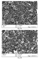
Voltage: 10V, Electrode distance 2 cm, CD=100 mA/cm2, Time 20/20/20 s (three 20 second intervals). Multiple deposition periods were adopted to reduce through-the-layer cracks. Electron micrographs of the resultant films are shown in FIGS. 5A and 5B, at varying magnification.
Example 4
A deposition was conducted of titania films on 500 nm thick copper sputtered on a polyimide (PI) surface under the following conditions:
Solution: Methanol:Water=95:5 v/v, TiCl4=0.02 M. (without H2O2 in the electrolyte.)
Voltage: 10V, Electrode distance 2 cm, CD=15 mA/cm2, Time 120 s
The process, which did not use hydrogen peroxide, produces a very porous structure, with evident cracking at lower magnifications, as shown in FIGS. 6A, 6B and 6C.
Example 5
The effect of methanol on titania film deposition was investigated. FIG. 7A shows a micrograph of a titania film formed in methanol+water, while FIG. 8A shows a corresponding film formed in water without methanol. FIGS. 7B and 8B show X-ray spectrograms of samples formed in a solution of [TiCl4]=0.004M, [H2O2]=0.02M, wherein chloride peaks are evident in the water solution process that are not evident in the water-methanol process.
Example 6
Titania films formed using the conditions specified had the following properties:
TABLE 1
Sample 1 2 3
Solution conditions CH3OH:H2O = 95:5 CH3OH:H2O = 95:5 CH3OH:H2O = 95:5
TiClO4 0.02M H2O2 0.1M TiClO4 0.01M H2O2 0.05M TiClO4 0.02M H2O2 0.1M
Deposition conditions
10 V, 20/20/20/20/20 s 10 V, 20/20 s 7 V, 20/20/20/20 s
Thickness (μm) 2 1.5 1
Area × 106 (m2) 0.8945 1.445 0.99 1.314 1.22 0.8959
Capacitance (nF) 0.166 0.327 0.192 0.249 0.671 0.313
Capacitance/Area 120 146 126 123 355 225
(nF/sq. in)
Dielectric constant 40 53 33 33 62 39

Using an HP Impedance analyzer and Agilent 34405A DMM for capacitance measurement, the following results were obtained:
TABLE 2
Sample 1 Sample 2
Thickness (μm) 2 1.5
Area × 106 (m2) 0.8945 1.445
Capacitance (nF) 100 kHz 0.124 0.249 0.142 0.217
Capacitance (nF) 1 MHz 0.082 0.176 0.104 0.156
Dielectric loss 100 kHz 0.0043 0.004 0.005 0.0069
Dielectric loss 1 MHz 0.51 0.52 0.64 0.67
Capacitance/Area 100 kHz 89.50 111.21 92.50 106.52
(nF/sq. in)
Capacitance/Area 1 MHz 59.16 78.60 67.75 76.58
(nF/sq. in)
Dielectric 100 kHz 31.31 38.92 24.29 27.97
constant
Dielectric
1 MHz 20.70 27.51 17.80 20.11
constant
Example 7
A barium salt (BaCl2), is added to the solution to provide Ba2+ ions. Titanium precursor solution (TiCl4) as well as TiO2 particles are converted to barium titanate (BaTiO3) in the barium-salt containing solution of higher pH. It is noted that the high pH solution is normally corrosive to the copper substrate.
The general reaction is:
Ba2++TiO2(s)+H2O→BaTiO3(s)+2H+
The phase diagram of this solution is shown in FIG. 9, which shows that higher [Ba2+] and higher pH favor formation of BaTiO3. Mild heating of between 55-80° C. speeds the reaction. This high pH is, however, corrosive to the copper layer.
The copper layer, however, may be protected by application of an electrochemical bias. FIG. 10 shows an EH-PH graph for the Cu—O2—H2O system, relevant during the conversion of titania to barium titante. At a pH of 12, a voltage bias of about −0.5V is required to maintain copper in the reduced state, with no considerable oxidation. Greater negative bias voltages will cause hydrolysis of water and generation of hydrogen, which will cause the titania film to peel off of the copper.
Example 8
Original titania films are made from multiple deposition cycles of 20-40-20-10 s. The resulting film thickness is 1.5 micron. The resulting film sample was treated with 0.01M BaCl2 aqueous solution, with the pH maintained at 12.3 with 5 M KOH. The process was conducted at a temperature of 75° C. The resultant film had the following properties:
TABLE 3
Original Titania Sample Converted Sample 1 Converted Sample 2
Thickness (μm) 1.5 1.5 1.5
Area * 106 (m2) 0.8459 1.2347 0.6570 1.2045 0.7173 1.1845
Capacitance (nF) 0.167 0.242 0.211 0.401 0.231 0.385
C/A (nF/sq. in 127.38 126.43 207.27 214.78 207.73 209.69
Dielectric constant 33.5 33.2 54.1 56.34 54.67 55.13
TiO2 thin films were thus fabricated on copper substrates during a low-temperature (room temperature) process for producing embedded capacitors.
The process parameters, e.g., temperature, voltage, solution composition, pH, etc., are derived from thermodynamic calculations for protection of the metallic cathode, which is in a preferred embodiment copper, but may of course be another conductive material which is, for example, subject to corrosion in aqueous TiCl4 or highly basic solutions.
Multiple deposition cycles are employed to avoid the “through-the-layer” cracks. Indeed, the process is generally controlled to produce a homogeneous film. On the other hand, it may be desirable to intentionally produce discrete layers, for example by selectively controlling conditions for each cycle, to produce a laminated structure of relatively homogeneous or heterogeneous composition. Further, in addition to changes in electric conditions over time, the solution may also be altered, to provide a heterogeneous layered structure and/or to permit post deposition transformation of a layer.
An optional SAM or other patterning layer may be provided on the cathode, to assist in organizing the deposited layers, though this is not required.
The process limits hydrogen evolution near the substrate, and results in good adhesion and dense microstructures.
The electrical performance of TiO2 thin film capacitors produced using the process was as follows:
Capacitance density: >120 nF/in2 (>59 nF/in2 at 1 MHz) (cf. 10 nF/in2 for commercially available ceramic particle polymer capacitors at 1 kHz)
Dielectric constant: >30 (>18 at 1 MHz).
Dielectric loss: <0.007 (at 100 kHz), <0.6 (at 1 MHz).
Breakdown voltage: >15 volts
The layer may be post-processed to transform the material. For example, a TiO2 layer may be converted to BaTiO3 by a conversion process. In thin Films, the obtained dielectric constant of BaTiO3 is >50, which represents, for example, a 67% increase over the starting TiO2 film material. The TiO2 film is converted to BaTiO3 at 55° C., pH=11.5-12.5 by 0.01 M BaCl2 in aqueous solution. This process generates acid (H+) near the cathode, and therefore the solution is titrated with KOH to maintain pH within the desired range during the process.
It is this seen that the present invention provides a method for forming films on a substrate susceptible to corrosion during film-formation or processing, which comprises providing electrodic protection of the substrate from corrosion, and limiting electrolysis of water near the substrate to improve film adhesion to the substrate. The film is preferably a titanium based dielectric, and the forming solution is preferably a ceramic precursor salt and a peroxide in a methanol-water media. The dielectric may be patterned on the substrate using a self-assembling monolayer mask.

Claims (31)

What is claimed is:
1. A method of forming a ceramic film on a substrate having a conductive surface, comprising:
immersing the substrate having the conductive surface in an aqueous solution, wherein the solution has at least one corrosive solute which is corrosive to the conductive surface, within a corrosive range of a composition of the solution and a corrosive voltage potential of the conductive surface with respect to a counter electrode in the solution;
applying a cathodic voltage potential on the conductive surface with respect to the counter electrode and controlling the composition of the solution by adding at least one ceramic precursor, sufficient to subject the conductive surface to conditions outside the corrosive range to thermodynamically protect the conductive surface from corrosion by the corrosive solute, and to drive formation of the ceramic film on the conductive surface through at least one electrochemical oxidation reaction of the at least one ceramic precursor; and
maintaining the cathodic voltage potential and composition of the solution outside of the corrosive range to promote formation of the ceramic film on the conductive surface while limiting an extent of at least one corrosive electrochemical reaction of the corrosive solute proximate to the conductive surface, and limiting hydrolysis of water within the aqueous solution to reduce peeling of the ceramic film from the conductive surface for a sufficient duration to produce a desired thickness of the ceramic film on the conductive surface while preserving the conductive surface;
wherein the conductive surface comprises metallic copper;
wherein the ceramic film comprises titanium dioxide;
wherein the solution comprises hydrogen peroxide;
wherein the at least one ceramic precursor comprises titanium tetrachloride; and
wherein the cathodic voltage potential is between −5V and −10V.
2. The method according to claim 1, wherein the conductive surface is cathodically protected by application of a negative bias voltage with respect to a reference electrode in solution and a pH of the solution proximate to the conductive surface is maintained.
3. The method according to claim 1, wherein the solution comprises between about 50% and 95% methanol.
4. The method according to claim 1, wherein the solution comprises methanol-water-hydrogen peroxide solution.
5. The method according to claim 1, wherein the reactive solute comprises chloride ion.
6. The method according to claim 1, wherein the ceramic film forms a dielectric layer of a capacitor.
7. The method according to claim 1, wherein the formed ceramic film is subjected to a chemical reaction to form a modified ceramic film having a dielectric constant greater than a respective dielectric constant of the ceramic film.
8. The method according to claim 7, wherein the chemical reaction comprises reacting the formed ceramic film with an ionic solution, while controlling a pH proximate to the formed ceramic film and the cathodic voltage potential of the conductive substrate with respect to a reference electrode in the solution.
9. The method according to claim 8, wherein the ionic solution comprises barium, and the modified ceramic film having increased dielectric constant comprises barium titanate.
10. The method according to claim 1, further comprising forming a conductive layer over the ceramic film, to thereby sandwich the ceramic film between the conductive layer and the conductive surface.
11. The method according to claim 1, wherein a self-assembling monolayer is formed on the conductive surface to influence a deposition of the ceramic film.
12. The method according to claim 1, wherein the ceramic film is electrically conductive and acts as an electrically resistive material between the conductive surface and an electrode adjacent to the ceramic film.
13. The method according to claim 1, wherein the electrochemical reaction comprises a hydrolytic production of hydrogen.
14. The method according to claim 1, wherein the ceramic film is formed to thickness of greater than about 0.5 microns.
15. The method according to claim 1, wherein the maintaining step is conducted under a maximum process temperature of less than about 100° C.
16. The method according to claim 1, further comprising the step of altering the cathodic voltage potential over time.
17. The method according to claim 1, wherein the cathodic voltage potential is applied for an aggregate of between about 20 and 140 s to form the ceramic film.
18. The method according to claim 1, wherein the corrosive solute comprises a halide ion.
19. The method according to claim 1, wherein the thermodynamic protection comprises maintaining a cathodic voltage potential and a pH proximate to the conductive surface within a range determined by thermodynamic analysis to maintain the conductive surface in a reduced state.
20. The method according to claim 1, wherein the ceramic film comprises at least one of tin, indium, zinc, and barium.
21. The method according to claim 1, further comprising masking a portion of the conductive surface to selectively define a ceramic film deposition region.
22. The method according to claim 1, further comprising forming a series of ceramic film layers on the conductive surface.
23. The method according to claim 1, wherein the ceramic film has a resistivity of between about 25 and 100 Ohms per square.
24. The method according to claim 1, wherein the ceramic film has a dielectric constant of at least 17.
25. The method according to claim 1, wherein the ceramic film has a breakdown voltage of at least 15V.
26. A method of forming a ceramic film on a substrate having a conductive surface, comprising:
providing at least one conductive surface portion on a substrate, subject to corrosion by at least one component of a solution containing at least one ceramic film precursor;
immersing the substrate having the conductive surface portion in the solution;
forming the ceramic film on the substrate from the at least one ceramic film precursor, by applying a voltage potential to the conductive surface with respect to a counter electrode in the solution and converting at least one ceramic film precursor through an electrochemical reaction involving an oxidation of the at least one ceramic film precursor, for a sufficient time to promote formation of the film to a desired thickness, wherein the at least one film precursor is consumed and at least on byproduct generated in the solution; and
thermodynamically limiting corrosion of the conductive surface resulting from at least one reaction with the solution proximate to the conductive surface, by at least concurrently controlling:
the applied voltage potential within a protective range that cathodically protects the conductive surface from corrosion by the at least one component and limits hydrolysis of the solution to reduce peeling of the ceramic film from the conductive surface, and
a composition of the solution proximate to the conductive surface over time to at least partially compensate for a change in composition of the solution;
wherein the conductive surface comprises metallic copper;
wherein the ceramic film comprises titanium dioxide;
wherein the solution comprises hydrogen peroxide;
wherein the at least one ceramic film precursor comprises titanium tetrachloride; and
wherein the voltage potential is between −5V and −10V.
27. A method for forming an electrically functional ceramic film on a conductive substrate having a surface subject to corrosion by soluble metal salts, comprising:
immersing a substrate having a conductive portion in a solution comprising a soluble electrically functional ceramic film precursor comprising at least one soluble metal salt and a peroxide;
applying a cathodic voltage potential to the conductive portion with respect to a counter electrode in the solution and controlling a composition of the solution, sufficient to thermodynamically protect the conductive portion from corrosion by the at least one soluble metal salt, and drive formation of an electrically functional ceramic film on the conductive substrate through at least one oxidation reaction, while limiting a hydrogen gas evolution reaction proximate to the conductive portion to reduce peeling of the electrically functional ceramic film from the conductive portion; and
maintaining the applied cathodic voltage potential and controlling the composition of the solution proximate to the conductive surface for a sufficient duration to produce an electrically functional ceramic film adherent on the conductive portion substantially without corrosion of the conductive portion;
wherein the conductive portion comprises metallic copper;
wherein the ceramic film comprises titanium dioxide;
wherein the peroxide comprises hydrogen peroxide;
wherein the at least one soluble metal salt comprises titanium tetrachloride; and
wherein the cathodic voltage potential is between −5V and −10V.
28. A method for forming functional film of a resistor or semiconductor on a portion of a substrate having a surface subject to corrosion by soluble metal salt ceramic precursors, comprising:
providing a substrate having a substrate portion;
depositing a resistive or semiconductive material ceramic film from a solution comprising a metal ion source and a peroxide on the substrate portion, by applying a cathodic voltage potential to the substrate portion with respect to a counter electrode in the solution, sufficient to protect the substrate portion from corrosion by the solution, and to drive formation of the resistive or semiconductive material ceramic film on the substrate portion through at least one oxidation reaction, while concurrently controlling a pH and limiting an extent of hydrolytic generation of hydrogen proximate to the substrate portion sufficient to reduce peeling of the resistive or semiconductive material ceramic film from the substrate portion after formation; and
forming a conductive portion on an exposed surface of the resistive or semiconductive material film;
wherein the substrate comprises metallic copper;
wherein the ceramic film comprises titanium dioxide;
wherein the peroxide comprises hydrogen peroxide;
wherein the metal ion source comprises titanium tetrachloride; and
wherein the cathodic voltage potential is between −5V and −10V.
29. A method of converting a titania film to a barium titanate film, comprising:
immersing a substrate having a titania film formed on conductive portion in a solution comprising a barium salt; and
applying a voltage potential to the conductive portion with respect to a counter electrode in the solution and a maintaning pH of the solution within a protective range which protects the conductive portion from corrosion by the solution which would otherwise occur under conditions of a voltage potential or a pH outside of the protective range, while limiting a production of hydrogen by hydrolysis proximate to the conductive portion to an extent sufficient to reduce peeling of the titania film from the conductive portion, to thereby permit conversion of the titania film to a barium titanate film; and
wherein the voltage potential is about −0.5V; and
wherein the pH is about 12.
30. The method according to claim 1, wherein the formed ceramic film is, or is transformed to be, a semiconductor.
31. The method according to claim 1, wherein the ceramic film is, or is transformed to be, a portion of a sensor.
US12/482,202 2008-06-10 2009-06-10 Embedded thin films Expired - Fee Related US8882983B2 (en)

Priority Applications (2)

Application Number Priority Date Filing Date Title
US12/482,202 US8882983B2 (en) 2008-06-10 2009-06-10 Embedded thin films
US14/537,123 US10064283B2 (en) 2008-06-10 2014-11-10 Embedded thin films

Applications Claiming Priority (3)

Application Number Priority Date Filing Date Title
US6044308P 2008-06-10 2008-06-10
US8716508P 2008-08-07 2008-08-07
US12/482,202 US8882983B2 (en) 2008-06-10 2009-06-10 Embedded thin films

Related Child Applications (1)

Application Number Title Priority Date Filing Date
US14/537,123 Continuation US10064283B2 (en) 2008-06-10 2014-11-10 Embedded thin films

Publications (2)

Publication Number Publication Date
US20090301770A1 US20090301770A1 (en) 2009-12-10
US8882983B2 true US8882983B2 (en) 2014-11-11

Family

ID=41399252

Family Applications (2)

Application Number Title Priority Date Filing Date
US12/482,202 Expired - Fee Related US8882983B2 (en) 2008-06-10 2009-06-10 Embedded thin films
US14/537,123 Active 2030-01-29 US10064283B2 (en) 2008-06-10 2014-11-10 Embedded thin films

Family Applications After (1)

Application Number Title Priority Date Filing Date
US14/537,123 Active 2030-01-29 US10064283B2 (en) 2008-06-10 2014-11-10 Embedded thin films

Country Status (1)

Country Link
US (2) US8882983B2 (en)

Cited By (1)

* Cited by examiner, † Cited by third party
Publication number Priority date Publication date Assignee Title
US10064283B2 (en) 2008-06-10 2018-08-28 The Research Foundation For The State University Of New York Embedded thin films

Families Citing this family (10)

* Cited by examiner, † Cited by third party
Publication number Priority date Publication date Assignee Title
US8784147B2 (en) 2009-06-09 2014-07-22 Tyco Electronics Corporation Composite assembly for an electrical connector and method of manufacturing the composite assembly
US8216006B2 (en) * 2009-06-09 2012-07-10 Tyco Electronics Corporation Composite assembly for an electrical connector and method of manufacturing the composite assembly
US8790144B2 (en) 2010-06-07 2014-07-29 Tyco Electronics Corporation Contact assembly for an electrical connector and method of manufacturing the contact assembly
EP2803083A4 (en) 2012-01-10 2014-12-31 Hzo Inc Masks for use in applying protective coatings to electronic assemblies, masked electronic assemblies and associated methods
US20130335898A1 (en) 2012-06-18 2013-12-19 Hzo, Inc. Systems and methods for applying protective coatings to internal surfaces of fully assembled electronic devices
JP5847663B2 (en) * 2012-08-01 2016-01-27 日本電子材料株式会社 Manufacturing method of probe card guide plate
US10449568B2 (en) 2013-01-08 2019-10-22 Hzo, Inc. Masking substrates for application of protective coatings
US9894776B2 (en) 2013-01-08 2018-02-13 Hzo, Inc. System for refurbishing or remanufacturing an electronic device
CN104245157B (en) 2013-01-08 2018-09-18 Hzo股份有限公司 The selected part of protective coating is removed from substrate
JP6054546B2 (en) * 2013-11-29 2016-12-27 シャープ株式会社 LIGHT EMITTING DEVICE SUBSTRATE, LIGHT EMITTING DEVICE, AND LIGHT EMITTING DEVICE SUBSTRATE MANUFACTURING METHOD

Citations (14)

* Cited by examiner, † Cited by third party
Publication number Priority date Publication date Assignee Title
US3273033A (en) * 1963-08-29 1966-09-13 Litton Systems Inc Multidielectric thin film capacitors
US4318795A (en) * 1967-12-14 1982-03-09 Diamond Shamrock Technologies S.A. Valve metal electrode with valve metal oxide semi-conductor face and methods of carrying out electrolysis reactions
US5328718A (en) * 1991-11-01 1994-07-12 Myrata Mfg., Co., Ltd. Production of barium titanate thin films
JPH11172489A (en) * 1997-12-09 1999-06-29 Murata Mfg Co Ltd Production of barium titanate coating film
US6030517A (en) * 1995-04-06 2000-02-29 Centre National De La Recherche Scientifique Process for preparing a film of an oxide or a hydroxide of an element of groups IIB or IIIA of the periodic table, and the composite structures which include such a film
US6261433B1 (en) * 1998-04-21 2001-07-17 Applied Materials, Inc. Electro-chemical deposition system and method of electroplating on substrates
US20020100693A1 (en) * 2001-02-01 2002-08-01 Jiong-Ping Lu Electrochemical reduction of copper seed for reducing ECD voids
US6503382B1 (en) * 1997-06-27 2003-01-07 University Of Southampton Method of electrodepositing a porous film
US20040099535A1 (en) * 2000-05-06 2004-05-27 Mattias Schweinsberg Electrochemically produced layers for providing corrosion protection or wash primers
US6793796B2 (en) * 1998-10-26 2004-09-21 Novellus Systems, Inc. Electroplating process for avoiding defects in metal features of integrated circuit devices
US20050051434A1 (en) * 2003-09-05 2005-03-10 Koji Mishima Method and apparatus for controlling electrolytic solution
US20070095657A1 (en) * 2005-11-02 2007-05-03 Kim Dong-Young Metal oxide supercapacitor having metal oxide electrode coated onto titanium dioxide ultrafine fiber and method for preparing the same
US20070148479A1 (en) * 2003-12-22 2007-06-28 Hiroki Ishikazi Corrosion-protection by electrochemical deposition of metal oxide layers on metal substrates
US8101059B2 (en) * 2008-02-28 2012-01-24 Corning Incorporated Methods of making titania nanostructures

Family Cites Families (3)

* Cited by examiner, † Cited by third party
Publication number Priority date Publication date Assignee Title
KR100638890B1 (en) 2005-10-04 2006-10-27 삼성전기주식회사 Coating solution for thin film having high dielectric and preparing method for dielectric thin film using it
JP2008204980A (en) * 2007-02-16 2008-09-04 Matsushita Electric Ind Co Ltd Multilayer ceramic substrate and manufacturing method therefor
US8882983B2 (en) 2008-06-10 2014-11-11 The Research Foundation For The State University Of New York Embedded thin films

Patent Citations (14)

* Cited by examiner, † Cited by third party
Publication number Priority date Publication date Assignee Title
US3273033A (en) * 1963-08-29 1966-09-13 Litton Systems Inc Multidielectric thin film capacitors
US4318795A (en) * 1967-12-14 1982-03-09 Diamond Shamrock Technologies S.A. Valve metal electrode with valve metal oxide semi-conductor face and methods of carrying out electrolysis reactions
US5328718A (en) * 1991-11-01 1994-07-12 Myrata Mfg., Co., Ltd. Production of barium titanate thin films
US6030517A (en) * 1995-04-06 2000-02-29 Centre National De La Recherche Scientifique Process for preparing a film of an oxide or a hydroxide of an element of groups IIB or IIIA of the periodic table, and the composite structures which include such a film
US6503382B1 (en) * 1997-06-27 2003-01-07 University Of Southampton Method of electrodepositing a porous film
JPH11172489A (en) * 1997-12-09 1999-06-29 Murata Mfg Co Ltd Production of barium titanate coating film
US6261433B1 (en) * 1998-04-21 2001-07-17 Applied Materials, Inc. Electro-chemical deposition system and method of electroplating on substrates
US6793796B2 (en) * 1998-10-26 2004-09-21 Novellus Systems, Inc. Electroplating process for avoiding defects in metal features of integrated circuit devices
US20040099535A1 (en) * 2000-05-06 2004-05-27 Mattias Schweinsberg Electrochemically produced layers for providing corrosion protection or wash primers
US20020100693A1 (en) * 2001-02-01 2002-08-01 Jiong-Ping Lu Electrochemical reduction of copper seed for reducing ECD voids
US20050051434A1 (en) * 2003-09-05 2005-03-10 Koji Mishima Method and apparatus for controlling electrolytic solution
US20070148479A1 (en) * 2003-12-22 2007-06-28 Hiroki Ishikazi Corrosion-protection by electrochemical deposition of metal oxide layers on metal substrates
US20070095657A1 (en) * 2005-11-02 2007-05-03 Kim Dong-Young Metal oxide supercapacitor having metal oxide electrode coated onto titanium dioxide ultrafine fiber and method for preparing the same
US8101059B2 (en) * 2008-02-28 2012-01-24 Corning Incorporated Methods of making titania nanostructures

Non-Patent Citations (5)

* Cited by examiner, † Cited by third party
Title
Bendale et al. ("Preparation of Barium Titanate Film at 55° C by an Electrochemical Method," J. Am. Ceram. Soc., 76 (10), 2619-27, 1993). *
Bunker, B.C., et al., "Ceramic thin-film formation on functionalized interfaces through biomimetic processing", Science, 264, 48 (1994).
Kajiyoshi et al. (Preparation of Tetragonal Barium Titanate Thin Film on Titanium Metal S Kajiyoshi et al. Kajiyoshi et al. Ubstrate by Hydrothermal Method, J. Am. Ceram. Soc., 74 (2), 369-374, 1991). *
Sameh et al., Corrosion of Copper in Deaerated and Oxygenated 0.1 M H2SO4 Solutions under Controlled Conditions of Mass Transfer, Eng. & Tech. Journal, vol. 27, No. 5, 2009. *
Smith, R.K., et al., "Patterning self-assembled monolayers", Progress in Surface Science 75, 1-68 (2004).

Cited By (1)

* Cited by examiner, † Cited by third party
Publication number Priority date Publication date Assignee Title
US10064283B2 (en) 2008-06-10 2018-08-28 The Research Foundation For The State University Of New York Embedded thin films

Also Published As

Publication number Publication date
US20160135303A1 (en) 2016-05-12
US20090301770A1 (en) 2009-12-10
US20170013721A9 (en) 2017-01-12
US10064283B2 (en) 2018-08-28

Similar Documents

Publication Publication Date Title
US8882983B2 (en) Embedded thin films
CN104039695B (en) Redox graphene and its production method
Gao et al. Site-selective deposition and micropatterning of SrTiO3 thin film on self-assembled monolayers by the liquid phase deposition method
KR20010050865A (en) Method for patterning, and electronic elements, optical elements and circuit substrates patterned therefrom
JP2006140454A (en) Capacitor structure
KR20110121628A (en) Conductive substrate
JPWO2008078652A1 (en) Dielectric element and manufacturing method thereof
KR20110010093A (en) Dielectric film, dielectric element, and process for producing the dielectric element
Maino et al. Electrochemically assisted deposition of transparent, mechanically robust TiO 2 films for advanced applications
JP2013502709A (en) Dielectric protective layer for self-assembled monolayer (SAM)
KR100857590B1 (en) Method for Room Temperature Chemical Vapor Deposition on Flexible Polymer Substrates
CN109741881B (en) Graphene flexible electrode and preparation method thereof
Taroata et al. High integration density capacitors directly integrated in a single copper layer of printed circuit boards
CN103596374B (en) The method forming conducting wire on flexible PCB
JP4184407B2 (en) Circuit board peelable foil
US7718552B2 (en) Nanostructured titania
CN113764283B (en) Method for manufacturing wiring substrate
EP2109124B1 (en) Capacitor material, method for manufacturing the capacitor material, capacitor containing the capacitor material, wiring board and electronic device
Gandhi et al. High-$ k $ thin-film capacitors with conducting oxide electrodes on glass substrates for power-supply applications
Hou et al. Low-Temperature Hydrothermal Deposition of (Ba x Sr1− x) TiO3 Thin Films on Flexible Polymeric Substrates for Embedded Applications
Ghosh et al. Hybrid dielectric thin films on flexible substrates for embedded capacitor applications
Roy et al. Electrodeposition of Titania Thin Films on Metallic Surface for High‐k Dielectric Applications
US8784147B2 (en) Composite assembly for an electrical connector and method of manufacturing the composite assembly
JP4944707B2 (en) Manufacturing method of gas sensor
CN113811081B (en) Method for manufacturing wiring substrate

Legal Events

Date Code Title Description
AS Assignment

Owner name: THE RESEARCH FOUNDATION FOR THE STATE UNIVERSITY OF NEW YORK, NEW YORK

Free format text: CHANGE OF NAME;ASSIGNOR:THE RESEARCH FOUNDATION OF STATE UNIVERSITY OF NEW YORK;REEL/FRAME:031896/0589

Effective date: 20120619

Owner name: THE RESEARCH FOUNDATION FOR THE STATE UNIVERSITY O

Free format text: CHANGE OF NAME;ASSIGNOR:THE RESEARCH FOUNDATION OF STATE UNIVERSITY OF NEW YORK;REEL/FRAME:031896/0589

Effective date: 20120619

AS Assignment

Owner name: THE RESEARCH FOUNDATION OF STATE UNIVERSITY OF NEW

Free format text: ASSIGNMENT OF ASSIGNORS INTEREST;ASSIGNORS:CHO, JUNGHYUN;SAMMAKIA, BAHGAT;ROY, BIPLAB KUMAR;SIGNING DATES FROM 20090604 TO 20090605;REEL/FRAME:033873/0176

STCF Information on status: patent grant

Free format text: PATENTED CASE

MAFP Maintenance fee payment

Free format text: PAYMENT OF MAINTENANCE FEE, 4TH YEAR, LARGE ENTITY (ORIGINAL EVENT CODE: M1551)

Year of fee payment: 4

FEPP Fee payment procedure

Free format text: ENTITY STATUS SET TO SMALL (ORIGINAL EVENT CODE: SMAL)

MAFP Maintenance fee payment

Free format text: PAYMENT OF MAINTENANCE FEE, 4TH YR, SMALL ENTITY (ORIGINAL EVENT CODE: M2551)

Year of fee payment: 4

REFU Refund

Free format text: REFUND - PAYMENT OF MAINTENANCE FEE, 4TH YEAR, LARGE ENTITY (ORIGINAL EVENT CODE: R1551)

FEPP Fee payment procedure

Free format text: MAINTENANCE FEE REMINDER MAILED (ORIGINAL EVENT CODE: REM.); ENTITY STATUS OF PATENT OWNER: SMALL ENTITY

LAPS Lapse for failure to pay maintenance fees

Free format text: PATENT EXPIRED FOR FAILURE TO PAY MAINTENANCE FEES (ORIGINAL EVENT CODE: EXP.); ENTITY STATUS OF PATENT OWNER: SMALL ENTITY

STCH Information on status: patent discontinuation

Free format text: PATENT EXPIRED DUE TO NONPAYMENT OF MAINTENANCE FEES UNDER 37 CFR 1.362

FP Lapsed due to failure to pay maintenance fee

Effective date: 20221111