US8884357B2 - Vertical NAND and method of making thereof using sequential stack etching and landing pad - Google Patents

Vertical NAND and method of making thereof using sequential stack etching and landing pad Download PDF

Info

Publication number
US8884357B2
US8884357B2 US14/219,161 US201414219161A US8884357B2 US 8884357 B2 US8884357 B2 US 8884357B2 US 201414219161 A US201414219161 A US 201414219161A US 8884357 B2 US8884357 B2 US 8884357B2
Authority
US
United States
Prior art keywords
control gate
semiconductor channel
gate electrode
channel
memory
Prior art date
Legal status (The legal status is an assumption and is not a legal conclusion. Google has not performed a legal analysis and makes no representation as to the accuracy of the status listed.)
Active
Application number
US14/219,161
Other versions
US20140284697A1 (en
Inventor
Chi-Ming Wang
Johann Alsmeier
Henry Chien
Xiying Costa
Yung-Tin Chen
Christopher Petti
Current Assignee (The listed assignees may be inaccurate. Google has not performed a legal analysis and makes no representation or warranty as to the accuracy of the list.)
SanDisk Technologies LLC
Original Assignee
SanDisk Technologies LLC
Priority date (The priority date is an assumption and is not a legal conclusion. Google has not performed a legal analysis and makes no representation as to the accuracy of the date listed.)
Filing date
Publication date
Priority claimed from PCT/US2014/023276 external-priority patent/WO2014164710A1/en
Application filed by SanDisk Technologies LLC filed Critical SanDisk Technologies LLC
Priority to US14/219,161 priority Critical patent/US8884357B2/en
Assigned to SANDISK TECHNOLOGIES INC. reassignment SANDISK TECHNOLOGIES INC. ASSIGNMENT OF ASSIGNORS INTEREST (SEE DOCUMENT FOR DETAILS). Assignors: ALSMEIER, JOHANN, CHEN, YUNG-TIN, CHIEN, HENRY, COSTA, XIYING, PETTI, CHRISTOPHER, WANG, CHI-MING
Publication of US20140284697A1 publication Critical patent/US20140284697A1/en
Application granted granted Critical
Publication of US8884357B2 publication Critical patent/US8884357B2/en
Assigned to SANDISK TECHNOLOGIES LLC reassignment SANDISK TECHNOLOGIES LLC CHANGE OF NAME (SEE DOCUMENT FOR DETAILS). Assignors: SANDISK TECHNOLOGIES INC
Active legal-status Critical Current
Anticipated expiration legal-status Critical

Links

Images

Classifications

    • HELECTRICITY
    • H10SEMICONDUCTOR DEVICES; ELECTRIC SOLID-STATE DEVICES NOT OTHERWISE PROVIDED FOR
    • H10BELECTRONIC MEMORY DEVICES
    • H10B43/00EEPROM devices comprising charge-trapping gate insulators
    • H01L27/11563
    • HELECTRICITY
    • H01ELECTRIC ELEMENTS
    • H01LSEMICONDUCTOR DEVICES NOT COVERED BY CLASS H10
    • H01L29/00Semiconductor devices adapted for rectifying, amplifying, oscillating or switching, or capacitors or resistors with at least one potential-jump barrier or surface barrier, e.g. PN junction depletion layer or carrier concentration layer; Details of semiconductor bodies or of electrodes thereof  ; Multistep manufacturing processes therefor
    • H01L29/66Types of semiconductor device ; Multistep manufacturing processes therefor
    • H01L29/66007Multistep manufacturing processes
    • H01L29/66075Multistep manufacturing processes of devices having semiconductor bodies comprising group 14 or group 13/15 materials
    • H01L29/66227Multistep manufacturing processes of devices having semiconductor bodies comprising group 14 or group 13/15 materials the devices being controllable only by the electric current supplied or the electric potential applied, to an electrode which does not carry the current to be rectified, amplified or switched, e.g. three-terminal devices
    • H01L29/66409Unipolar field-effect transistors
    • H01L29/66477Unipolar field-effect transistors with an insulated gate, i.e. MISFET
    • H01L29/66825Unipolar field-effect transistors with an insulated gate, i.e. MISFET with a floating gate
    • HELECTRICITY
    • H01ELECTRIC ELEMENTS
    • H01LSEMICONDUCTOR DEVICES NOT COVERED BY CLASS H10
    • H01L29/00Semiconductor devices adapted for rectifying, amplifying, oscillating or switching, or capacitors or resistors with at least one potential-jump barrier or surface barrier, e.g. PN junction depletion layer or carrier concentration layer; Details of semiconductor bodies or of electrodes thereof  ; Multistep manufacturing processes therefor
    • H01L29/66Types of semiconductor device ; Multistep manufacturing processes therefor
    • H01L29/66007Multistep manufacturing processes
    • H01L29/66075Multistep manufacturing processes of devices having semiconductor bodies comprising group 14 or group 13/15 materials
    • H01L29/66227Multistep manufacturing processes of devices having semiconductor bodies comprising group 14 or group 13/15 materials the devices being controllable only by the electric current supplied or the electric potential applied, to an electrode which does not carry the current to be rectified, amplified or switched, e.g. three-terminal devices
    • H01L29/66409Unipolar field-effect transistors
    • H01L29/66477Unipolar field-effect transistors with an insulated gate, i.e. MISFET
    • H01L29/66833Unipolar field-effect transistors with an insulated gate, i.e. MISFET with a charge trapping gate insulator, e.g. MNOS transistors
    • HELECTRICITY
    • H01ELECTRIC ELEMENTS
    • H01LSEMICONDUCTOR DEVICES NOT COVERED BY CLASS H10
    • H01L29/00Semiconductor devices adapted for rectifying, amplifying, oscillating or switching, or capacitors or resistors with at least one potential-jump barrier or surface barrier, e.g. PN junction depletion layer or carrier concentration layer; Details of semiconductor bodies or of electrodes thereof  ; Multistep manufacturing processes therefor
    • H01L29/66Types of semiconductor device ; Multistep manufacturing processes therefor
    • H01L29/68Types of semiconductor device ; Multistep manufacturing processes therefor controllable by only the electric current supplied, or only the electric potential applied, to an electrode which does not carry the current to be rectified, amplified or switched
    • H01L29/76Unipolar devices, e.g. field effect transistors
    • H01L29/772Field effect transistors
    • H01L29/78Field effect transistors with field effect produced by an insulated gate
    • H01L29/788Field effect transistors with field effect produced by an insulated gate with floating gate
    • H01L29/7889Vertical transistors, i.e. transistors having source and drain not in the same horizontal plane
    • HELECTRICITY
    • H01ELECTRIC ELEMENTS
    • H01LSEMICONDUCTOR DEVICES NOT COVERED BY CLASS H10
    • H01L29/00Semiconductor devices adapted for rectifying, amplifying, oscillating or switching, or capacitors or resistors with at least one potential-jump barrier or surface barrier, e.g. PN junction depletion layer or carrier concentration layer; Details of semiconductor bodies or of electrodes thereof  ; Multistep manufacturing processes therefor
    • H01L29/66Types of semiconductor device ; Multistep manufacturing processes therefor
    • H01L29/68Types of semiconductor device ; Multistep manufacturing processes therefor controllable by only the electric current supplied, or only the electric potential applied, to an electrode which does not carry the current to be rectified, amplified or switched
    • H01L29/76Unipolar devices, e.g. field effect transistors
    • H01L29/772Field effect transistors
    • H01L29/78Field effect transistors with field effect produced by an insulated gate
    • H01L29/792Field effect transistors with field effect produced by an insulated gate with charge trapping gate insulator, e.g. MNOS-memory transistors
    • H01L29/7926Vertical transistors, i.e. transistors having source and drain not in the same horizontal plane
    • HELECTRICITY
    • H10SEMICONDUCTOR DEVICES; ELECTRIC SOLID-STATE DEVICES NOT OTHERWISE PROVIDED FOR
    • H10BELECTRONIC MEMORY DEVICES
    • H10B41/00Electrically erasable-and-programmable ROM [EEPROM] devices comprising floating gates
    • H10B41/20Electrically erasable-and-programmable ROM [EEPROM] devices comprising floating gates characterised by three-dimensional arrangements, e.g. with cells on different height levels
    • H10B41/23Electrically erasable-and-programmable ROM [EEPROM] devices comprising floating gates characterised by three-dimensional arrangements, e.g. with cells on different height levels with source and drain on different levels, e.g. with sloping channels
    • H10B41/27Electrically erasable-and-programmable ROM [EEPROM] devices comprising floating gates characterised by three-dimensional arrangements, e.g. with cells on different height levels with source and drain on different levels, e.g. with sloping channels the channels comprising vertical portions, e.g. U-shaped channels
    • HELECTRICITY
    • H10SEMICONDUCTOR DEVICES; ELECTRIC SOLID-STATE DEVICES NOT OTHERWISE PROVIDED FOR
    • H10BELECTRONIC MEMORY DEVICES
    • H10B43/00EEPROM devices comprising charge-trapping gate insulators
    • H10B43/20EEPROM devices comprising charge-trapping gate insulators characterised by three-dimensional arrangements, e.g. with cells on different height levels
    • H10B43/23EEPROM devices comprising charge-trapping gate insulators characterised by three-dimensional arrangements, e.g. with cells on different height levels with source and drain on different levels, e.g. with sloping channels
    • H10B43/27EEPROM devices comprising charge-trapping gate insulators characterised by three-dimensional arrangements, e.g. with cells on different height levels with source and drain on different levels, e.g. with sloping channels the channels comprising vertical portions, e.g. U-shaped channels
    • HELECTRICITY
    • H10SEMICONDUCTOR DEVICES; ELECTRIC SOLID-STATE DEVICES NOT OTHERWISE PROVIDED FOR
    • H10BELECTRONIC MEMORY DEVICES
    • H10B69/00Erasable-and-programmable ROM [EPROM] devices not provided for in groups H10B41/00 - H10B63/00, e.g. ultraviolet erasable-and-programmable ROM [UVEPROM] devices

Definitions

  • the present invention relates generally to the field of semiconductor devices and specifically to three dimensional vertical NAND strings and other three dimensional devices and methods of making thereof.
  • FIGS. 1A and 1B Examples of prior art three dimensional vertical NAND strings are illustrated in FIGS. 1A and 1B .
  • the device shown in FIG. 1A is known in the art as terabit cell array transistor (“TCAT”) array. It includes damascened metal gate SONOS type cells in the vertical NAND flash string formed by a gate replacement process (see Jang, et al., “Vertical cell array using TCAT (Terabit Cell Array Transistor) technology for ultra high density NAND flash memory,” 2009 Symposium on VLSI Technology Digest of Technical Papers, pages 192-193, Jun. 16, 2009, Honolulu, Hi., incorporated herein by reference in its entirety).
  • TCAT terabit cell array transistor
  • P-BiCS Pipe-shaped Bit Cost Scalable
  • One embodiment includes a vertical NAND string device including a semiconductor channel, wherein at least one end portion of the semiconductor channel extends substantially perpendicular to a major surface of a substrate, at least one semiconductor or electrically conductive landing pad embedded in the semiconductor channel, a tunnel dielectric located adjacent to the semiconductor channel, a charge storage region located adjacent to the tunnel dielectric, a blocking dielectric located adjacent to the charge storage region and a plurality of control gate electrodes extending substantially parallel to the major surface of the substrate.
  • the plurality of control gate electrodes include at least a first control gate electrode located in a first device level and a second control gate electrode located in a second device level located over the major surface of the substrate and below the first device level.
  • the landing pad has a larger width than a widest portion of the channel, tunnel dielectric, charge storage region and blocking dielectric.
  • Another embodiment includes a method of making a vertical NAND device including forming a lower portion of the memory stack over a substrate, forming a lower portion of memory openings in the lower portion of the memory stack, forming at least one additional portion of the memory stack over the lower portion of the memory stack, forming at least one additional portion of the memory openings in the at least one additional portion of the memory stack, forming a lower portion of the semiconductor channels in the lower portion of the memory openings, forming semiconductor or electrically conductive landing pads in contact with the lower semiconductor channel portions, wherein the landing pads have a larger width than a widest portion of the memory openings and forming at least one additional portion of the semiconductor channels in the at least one additional portion of the memory openings, such that the at least one additional portion of the semiconductor channels contacts the respective landing pads.
  • Another embodiment includes a method of making a vertical NAND device including forming a lower portion of the memory stack over a substrate, forming a lower portion of memory openings in the lower portion of the memory stack, forming at least one additional portion of the memory stack over the lower portion of the memory stack, forming at least one additional portion of the memory openings in the at least one additional portion of the memory stack, forming a lower portion of the semiconductor channels in the lower portion of the memory openings, forming semiconductor or electrically conductive landing pads in contact with the lower semiconductor channel portions, forming at least one additional portion of the semiconductor channels in the at least one additional portion of the memory openings, such that the at least one additional portion of the semiconductor channels contacts the respective landing pads, filling lower parts of the lower portion of the memory openings with a sacrificial material, widening remaining exposed top parts of the lower portion of the memory openings where the landing pads will be subsequently formed and filling the widened top parts of the lower portion of the memory openings with a sacrificial material.
  • a vertical NAND string device including a mixed metal oxide semiconductor channel, wherein at least one end portion of the semiconductor channel extends substantially perpendicular to a major surface of a substrate, a tunnel dielectric located adjacent to the semiconductor channel, a charge storage region located adjacent to the tunnel dielectric, a blocking dielectric located adjacent to the charge storage region and a plurality of control gate electrodes extending substantially parallel to the major surface of the substrate, wherein the plurality of control gate electrodes include at least a first control gate electrode located in a first device level and a second control gate electrode located in a second device level located over the major surface of the substrate and below the first device level.
  • a vertical NAND string device including a semiconductor channel, wherein at least one end portion of the semiconductor channel extends substantially perpendicular to a major surface of a substrate, at least one semiconductor or electrically conductive landing pad embedded in the semiconductor channel.
  • the vertical NAND string device also includes a tunnel dielectric located adjacent to the semiconductor channel, a charge storage region located adjacent to the tunnel dielectric, a blocking dielectric located adjacent to the charge storage region and a stack comprising a plurality of control gate electrodes extending substantially parallel to the major surface of the substrate.
  • the plurality of control gate electrodes comprise at least a first control gate electrode located in a first device level and a second control gate electrode located in a second device level located over the major surface of the substrate and below the first device level.
  • the at least one landing pad is located between a select gate electrode and an end control gate electrode in the stack.
  • a vertical NAND string device including a semiconductor channel, wherein at least one end portion of the semiconductor channel extends substantially perpendicular to a major surface of a substrate, at least one semiconductor or electrically conductive current boosting layer electrically connected to the semiconductor channel and to a current or voltage source, a tunnel dielectric located adjacent to the semiconductor channel, a charge storage region located adjacent to the tunnel dielectric, a blocking dielectric located adjacent to the charge storage region and a plurality of control gate electrodes extending substantially parallel to the major surface of the substrate, wherein the plurality of control gate electrodes comprise at least a first control gate electrode located in a first device level and a second control gate electrode located in a second device level located over the major surface of the substrate and below the first device level.
  • Another embodiment includes a method of operating a vertical NAND string device having a semiconductor channel with at least one end portion of the semiconductor channel extending substantially perpendicular to a major surface of a substrate, including applying a voltage or current to at least one semiconductor or electrically conductive current boosting layer electrically connected to the semiconductor channel.
  • FIG. 1A is a side cross sectional views of a prior art NAND memory device.
  • FIG. 1B is a perspective cross sectional view of another prior art NAND memory device.
  • FIGS. 2A , 2 B, 3 A and 3 B are side cross sectional views of a NAND memory device of embodiments of the invention.
  • FIG. 3C is a top cross sectional view of the device of FIGS. 3A and 3B .
  • FIG. 2C is a top cross sectional view of NAND memory devices of FIGS. 2A and 2B .
  • FIGS. 2D and 2E are schematic circuit diagrams of the devices of FIGS. 2A and 2B , respectively.
  • FIG. 4A is a side cross sectional views of a NAND memory device of an embodiment of the invention.
  • FIG. 4B is a top cross sectional view of the device of FIG. 4A .
  • FIGS. 5A and 5B are perpendicular side cross sectional views along lines A-A′ and B-B′ in FIG. 5C of a lower select gate device level of the NAND memory device of an embodiment of the invention.
  • FIG. 5C is a top cross sectional view of the device of FIGS. 5A and 5B .
  • FIGS. 6A , 6 B, 6 C and 6 D are side cross sectional views of steps in the method of making the lower select gate device level of the NAND memory device of an embodiment of the invention.
  • FIGS. 7 , 8 , 9 and 10 are side cross sectional views of steps in the method of making the memory device levels of the NAND memory device of an embodiment of the invention.
  • FIGS. 11A and 11B are perpendicular side cross sectional views along lines A-A′ and B-B′ in FIG. 11C of an upper select gate device level of the NAND memory device of an embodiment of the invention.
  • FIG. 11C is a top cross sectional view of the device of FIGS. 11A and 11B .
  • FIGS. 12A and 12B are side cross sectional views of respective lower and upper select gate device level of the NAND memory device of an embodiment of the invention.
  • FIGS. 13A and 13B are side cross sectional views of NAND memory devices of other embodiments of the invention.
  • FIG. 14A is a top cross sectional view of the prior art device and FIGS. 14B and 14C are a top cross sectional views of NAND memory devices according to embodiments of the invention.
  • FIGS. 14D and 14E are respective side cross sectional views along lines A-A′ and B-B′ in FIG. 14C of a NAND memory device of an embodiment of the invention.
  • FIGS. 15A to 15K are side cross sectional views of steps in the method of making the NAND memory device shown in FIG. 2A .
  • FIGS. 16A to 16B are side cross sectional views of steps in the method of making the NAND memory device shown in FIG. 3A .
  • FIGS. 17A to 17H are side cross sectional views of steps in a method of overcoming misalignment of memory stacks in making a NAND memory device with at least two memory stacks.
  • FIGS. 18A to 18F are side cross sectional views of steps in method of making the NAND memory device with a current boosting layer according to another embodiment.
  • FIG. 18G is a cross sectional view of an alternative NAND memory device with a current boosting layer according to an embodiment.
  • FIGS. 19A to 19D are side cross sectional views of steps in the method of making the NAND memory device according to another embodiment.
  • FIG. 19E is a schematic circuit diagram of the device of FIG. 19D .
  • FIGS. 20A to 20J are side cross sectional views of steps in the method of making the NAND memory device shown in FIG. 2B .
  • Three dimensional (3D) vertical NAND devices requires etching of deep, high aspect ratio memory openings or holes for formation of the vertical channel due to a high number of stacked memory layers surrounding the vertical channels.
  • the terms “memory hole” and “memory opening” are used interchangeably herein.
  • a memory layer includes a control gate and associated charge storage region (e.g., a dielectric isolated floating gate, an ONO stack, etc.) and at least a portion of two dielectric isolation layers located above and below each control gate.
  • the hard mask thickness used during high aspect ratio etching limits of the maximum number of stacked memory layers in the vertical NAND because the amount of hard mask thickness consumed increases during memory opening etching with increasing amount of memory layers stacked in the memory structure. For example, for a 1500 nm thick hard mask, at most 35 memory layers may be etched using reactive ion etching (RIE) to form the memory opening before all of the hard mask thickness is consumed by the etching.
  • RIE reactive ion etching
  • RIE reactive ion etching
  • Increasing the hard mask thickness to increase the number of stacked memory levels is also not highly desirable because an increase in the hard mask thickness undesirably increases the aspect ratio of the opening.
  • RIE energy also limits the number of stacked memory layers in the vertical NAND.
  • the reactive ions are scattered within the high aspect memory opening during the etching, which leads to a decrease in the RIE energy.
  • the RIE energy will eventually be reduced to an extent at which the RIE process loses the capability to etch the memory opening. Therefore, with a smaller RIE energy, a lower number of memory layers can be etched at the same time.
  • increasing the RIE energy is also not highly desirable because it leads to increased back sputtering effects which may lead to control gate to control gate (i.e., word line to word line) shorts. Therefore, the RIE energy also limits the number of stacked memory layers in the vertical NAND.
  • the present inventors realized that the number of stacked memory layers in a vertical NAND may be increased if the portions of each memory openings are etched sequentially. Due to the limited depth of the opening in sequential etching, the high etching aspect etching ratio challenges noted above may be decreased.
  • a lower portion of the memory stack is formed over a substrate. This portion includes only a part of the memory layers that will be used in the vertical NAND.
  • the lower portions of the memory openings are etched in the lower portion of the memory stack.
  • at least one additional portion of the memory stack is formed over the lower portion of the memory stack.
  • the at least one additional portion of the memory stack contains additional memory levels.
  • additional portions of the memory openings are then etched in the at least one additional portion of the memory stack.
  • the at least one additional portion comprises an upper portion of the stack and the additional portions of the memory openings comprise upper portions of the memory openings. If the stack contains more than two portions, then the above process may be repeated several times. In this case, the at least one additional portion comprises one or more middle portions and an upper portion of the stack and the additional portions of the memory openings comprise one or more middle portions and upper portions of the memory openings.
  • each hard mask used during each etching step may be relatively thin and the hard mask thickness does not limit the total number of memory layers in the stack.
  • each RIE step of each memory opening portions forms an opening that has a limited depth, the RIE energy also does not limit the total number of memory layers in the stack.
  • each memory opening i.e., lower portion, upper portion and optionally one or more middle portions
  • the misalignment of the memory opening portions may lead to channel discontinuity which results in an open NAND string.
  • the present inventors realized that the memory opening alignment challenges may be reduced or avoided by adding a landing pad between the memory stack portions.
  • the landing pad is wider (e.g., had a larger diameter) than the channel in the horizontal direction.
  • the landing pad may be 10-100% wider, such as 25-75% wider than the channel (i.e., for disc shaped pads and cylindrical channels, the pad diameter is larger than the channel diameter by 10-100%).
  • the pad diameter i.e., width
  • the pad may be 20-50 nm, such as 30-40 nm thick.
  • the landing pad connects adjacent channel portions in adjacent memory opening portions of the same memory opening even if the memory opening portions are misaligned with respect to each other.
  • the landing pads contact the upper, widest portion of the memory openings.
  • the landing pad is wider than the widest portion of the memory openings.
  • the memory openings include a blocking dielectric, a charge storage region and a tunnel dielectric in addition to the channel.
  • the landing pad in preferably has a larger width than a widest portion of the channel, tunnel dielectric, charge storage region and blocking dielectric.
  • the landing pad may comprise any suitable semiconductor or electrical conductor material, such as silicon, metal, metal alloy, etc.
  • the landing pad is made of the same semiconductor material as the channel of the vertical NAND.
  • the landing pad may comprise a polysilicon landing pad if the channel is a polysilicon channel.
  • a semiconductor landing pad may be intrinsic or have the same conductivity type (e.g., p or n) as the channel.
  • the semiconductor landing pad may be heavier doped than the channel (e.g., heavily doped landing pad and lightly doped channel), have the same doping concentration as the channel or may be lighter doped than the channel.
  • the pad resistivity may be less than, greater than or the same as the resistivity of the channel material.
  • the landing pad may comprise a metal (e.g., Ti, W, etc.) or conductive metal alloys (e.g., TiN, WN, a metal silicide, such as titanium, tungsten, nickel, cobalt or platinum silicide, etc.).
  • a metal e.g., Ti, W, etc.
  • conductive metal alloys e.g., TiN, WN, a metal silicide, such as titanium, tungsten, nickel, cobalt or platinum silicide, etc.
  • the landing pad may be formed over each channel portion (except over the upper most channel portion if desired) during the same deposition step as the channel deposition step or during subsequent deposition step. Then, the next overlying channel portion is formed on the landing pad.
  • the landing pad may also be considered a resistor built into the vertical channel of the vertical NAND string.
  • the impact of the increase in resistance on the vertical NAND read performance due to the presence of the resistor should not be great.
  • the resistance value is 1.35 kOhm. If the stack includes five landing pads per channel or ten landing pads per U-shaped channel in a P-BiCS vertical NAND, then the total resistance is 13.5 kOhm for a 50 nm diameter memory opening. If a 400 nA read current is used in the NAND string, then the bit line voltage needs to increase by only 5 mV due to the ten additional series resistors/landing pads. Likewise, an additional thermal budget (e.g., MONOS anneal) may be added due to the presence of the landing pads. However, the thermal budget impact on the NAND string characteristics should be manageable.
  • MONOS anneal e.g., MONOS anneal
  • FIGS. 2A through 4B illustrate various non-limiting, exemplary VNAND devices containing a landing pad/built-in resistor.
  • FIGS. 2A and 2D illustrate a vertical NAND containing a landing pad/built-in resistor having a single vertical channel having a pillar type configuration.
  • FIGS. 2B and 2E illustrate a vertical NAND containing a landing pad/built-in resistor having a U-shaped (e.g., pipe shaped) channel having a “P-BiCS” type configuration.
  • FIG. 2C illustrates a top view of the devices in FIGS. 2A and 2B .
  • FIGS. 3A through 4B illustrate a vertical NAND containing a landing pad/built-in resistor having a compact vertical NAND (“CVNAND”) type configuration, which will be described in more detail below.
  • the CVNAND device is also described in more detail in U.S. patent application Ser. No. 13/754,293, filed on Jan. 30, 2013 and incorporated herein by reference in its entirety.
  • the NAND string 180 illustrated in FIGS. 2A-4B may be formed with a vertical channel.
  • the vertical channel 1 has a solid, rod shape as shown in FIGS. 2A , 2 B, 3 B, 3 A and 4 B.
  • the entire channel comprises a semiconductor material.
  • the vertical channel has a hollow cylinder shape as shown in FIG. 4A .
  • the vertical channel includes a non-semiconductor core 2 surrounded by a semiconductor channel 1 shell. The core may be unfilled or filled with an insulating material, such as silicon oxide or silicon nitride.
  • the monolithic three dimensional NAND string 180 comprises a semiconductor channel 1 having at least one end portion extending substantially perpendicular to a major surface 100 a of a substrate 100 , as shown in FIGS. 2A , 2 D, 3 A and 3 B.
  • the semiconductor channel 1 may have a pillar shape and the entire pillar-shaped semiconductor channel extends substantially perpendicularly to the major surface 100 a of the substrate 100 .
  • the source/drain electrodes of the device can include a lower electrode 102 (e.g., a heavily doped semiconductor region source electrode in the major surface 100 a of a semiconductor substrate 100 ) provided below the semiconductor channel 1 (optionally in contact with a doped source region 103 ), and an upper electrode 202 (e.g., bit line) formed over the doped drain region 203 in the semiconductor channel 1 , as shown in FIG. 2A .
  • the lower electrode 102 contacts a metal interconnect outside of the view shown in FIGS. 2A and 3A or contacts metal wires of circuitry under the array.
  • the drain/bit line electrode 202 contacts the pillar-shaped semiconductor channel 1 (via the drain region 203 ) from above, and the source electrode 102 contacts the pillar-shaped semiconductor channel 1 from below (e.g., via source region 103 ).
  • 2A and 2D contains two levels of landing pads 25 , which divide the channel and the stack into three portions: lower portion of the stack 120 L containing the lower portions 1 xa , 1 xb of the wings 1 a , 1 b ; middle portion of the stack 120 M containing the middle portions 1 ya , 1 yb of the wings 1 a , 1 b ; and upper portion of the stack 120 U containing the upper portions 1 za , 1 zb of the wings 1 a , 1 b.
  • the NAND string may have a U shape (also known as a “pipe” shape) with two vertical channel wing portions connected with a horizontal channel connecting the wing portions.
  • the U shaped or pipe shaped channel may be solid, as in the solid rod shaped vertical channel NAND as shown in FIG. 2B .
  • the U shaped or pipe shaped channel may be hollow cylinder shaped, (similar to the hollow cylinder pipe shaped vertical channel NAND as shown in FIG. 4A ).
  • the U-shaped pipe channel may be filled or unfilled.
  • the two wing portions 1 a and 1 b of the U-shape semiconductor channel may extend substantially perpendicular to the major surface of the substrate, and a connecting portion 1 c of the U-shape semiconductor channel 1 connects the two wing portions 1 a , 1 b extends substantially perpendicular to the major surface of the substrate.
  • the wing portions 1 a , 1 b of the channel 1 contain the built-in landing pads/resistors 25 .
  • 2B and 2E contains two levels of landing pads 25 , which divide the channel and the stack into three portions: lower portion of the stack 120 L containing the lower portions 1 xa , 1 xb of the wings 1 a , 1 b ; middle portion of the stack 120 M containing the middle portions 1 ya , 1 yb of the wings 1 a , 1 b ; and upper portion of the stack 120 U containing the upper portions 1 za , 1 zb of the wings 1 a , 1 b.
  • one of the source or drain electrodes 202 contacts the first wing portion of the semiconductor channel from above, and another one of a source or drain electrodes (e.g., source line) 102 contacts the second wing portion of the semiconductor channel 1 from above.
  • An optional body contact electrode 91 may be disposed over or in the substrate to provide body contact to the connecting portion of the semiconductor channel 1 from below.
  • the NAND string's select or access transistors 16 are shown in FIGS. 2B and 2E . These transistors and their operation are described in U.S. Pat. No. 8,187,936, which is incorporated by reference for a teaching of the select transistors.
  • the device of FIGS. 2B and 2E is described in more detail below with reference to the method of making the P-BiCS type vertical NAND, as shown in FIGS. 17A-17H .
  • the substrate 100 can be any semiconducting substrate known in the art, such as monocrystalline silicon, IV-IV compounds such as silicon-germanium or silicon-germanium-carbon, III-V compounds, II-VI compounds, epitaxial layers over such substrates, or any other semiconducting or non-semiconducting material, such as silicon oxide, glass, plastic, metal or ceramic substrate.
  • the substrate 100 may include integrated circuits fabricated thereon, such as driver circuits for a memory device.
  • any suitable semiconductor materials can be used for semiconductor channel 1 , for example silicon, germanium, silicon germanium, indium antimonide, or other compound semiconductor materials, such as III-V or II-VI semiconductor materials.
  • the semiconductor material may be amorphous, polycrystalline or single crystal.
  • the semiconductor channel material may be formed by any suitable deposition methods.
  • the semiconductor channel material is deposited by low pressure chemical vapor deposition (LPCVD).
  • LPCVD low pressure chemical vapor deposition
  • the semiconductor channel material may be a recyrstallized polycrystalline semiconductor material formed by recrystallizing an initially deposited amorphous semiconductor material.
  • the insulating fill material 2 in FIG. 4A may comprise any electrically insulating material, such as silicon oxide, silicon nitride, silicon oxynitride, or other insulating materials.
  • Each monolithic three dimensional NAND string 180 further comprises a plurality of control gate electrodes 3 , as shown in FIGS. 2A , 2 B, 3 A, 3 B and 4 A- 4 B.
  • the control gate electrodes 3 may comprise a portion having a strip shape extending substantially parallel to the major surface 100 a of the substrate 100 .
  • the plurality of control gate electrodes 3 comprise at least a first control gate electrode 3 a located in a first device level (e.g., device level A) and a second control gate electrode 3 b located in a second device level (e.g., device level B) located over the major surface 100 a of the substrate 100 and below the device level A, as shown in FIGS. 2A , 2 B, 3 A and 4 A.
  • the control gate material may comprise any one or more suitable conductive or semiconductor control gate material known in the art, such as doped polysilicon or a metal, such as tungsten, copper, aluminum, tantalum, titanium, cobalt, titanium nitride or alloys thereof.
  • Each channel 1 shown in FIGS. 2A-4B contains one or more landing pads/built-in resistors 25 described above.
  • each landing pad 25 is located in a vertical position of the channel between control gates 3 (i.e., having one control gate above and one control gate below).
  • the landing pad is located between the first device level (e.g., level A) and the second device level (e.g., level B).
  • a lower portion of the semiconductor channel (e.g., 84 x ) located in the first device level contacts a bottom surface of the landing pad 25 .
  • a middle or upper portion (e.g., 84 y ) of the semiconductor channel located in the second device level contacts a top surface of the same landing pad 25 .
  • the landing pad 25 may extend horizontally beyond the memory hole 84 diameter or width to be located over and under adjacent control gates 3 inside the dielectric fill material 121 Thus, the landing pad 25 may extend into the insulating layer 121 between the first 3 a and the second 3 b control gate electrodes 3 .
  • the fill material 121 isolates the landing pad 25 from direct contact with the control gate electrodes 3 .
  • the landing pad 25 may be relatively thick and contact dummy control gate electrodes 3 d , as shown in FIGS. 17G and 17H .
  • Dummy control gate electrodes 3 d i.e., dummy word lines
  • a blocking dielectric 7 is located adjacent to and may be surrounded by the control gate(s) 3 .
  • the blocking dielectric 7 may comprise a continuous layer or a plurality of blocking dielectric segments located in contact with a respective one of the plurality of control gate electrodes 3 .
  • a first dielectric segment 7 a located in device level A and a second dielectric segment 7 b located in device level B are in contact with control electrodes 3 a and 3 b , respectively, as shown in FIG. 4A .
  • at least a portion of each of the plurality of blocking dielectric segments 7 surrounds the top, bottom, and two edge portions of a control gate electrode 3 between two adjacent NAND strings, as shown in FIGS. 3A and 4A .
  • the NAND devices also comprise one or more charge storage regions 9 located between the channel 1 and the blocking dielectric 7 .
  • the charge storage regions 9 may comprise a continuous vertical charge storage layer adjacent to plural control gate electrodes 3 , as shown in FIGS. 2A and 2B or the plurality of discrete charge storage regions 9 comprise at least a first discrete charge storage segment 9 a located in the device level A and a second discrete charge storage segment 9 b located in the device level B, as shown in FIG. 4A .
  • a tunnel dielectric 11 is located between the charge storage region(s) 9 and the semiconductor channel 1 .
  • the blocking dielectric 7 and the tunnel dielectric 11 may be independently selected from any one or more same or different electrically insulating materials, such as silicon oxide, silicon nitride, silicon oxynitride, or other insulating materials.
  • the charge storage region(s) 9 may comprise a conductive (e.g., metal or metal alloy such as titanium, platinum, ruthenium, titanium nitride, hafnium nitride, tantalum nitride, zirconium nitride, or a metal silicide such as titanium silicide, nickel silicide, cobalt silicide, or a combination thereof) or semiconductor (e.g., polysilicon) floating gate(s), conductive nanoparticles, or a charge storage dielectric layer or segment (e.g., silicon nitride or another dielectric).
  • a conductive e.g., metal or metal alloy such as titanium, platinum, ruthenium, titanium nitride, hafnium nitride, tantalum nitride, zirconium nitride, or a metal silicide such as titanium silicide, nickel silicide, cobalt silicide, or a combination thereof
  • semiconductor e.
  • the charge storage regions comprise silicon nitride, where the silicon oxide blocking dielectric 7 , the nitride charge storage region 9 and the silicon oxide tunnel dielectric 11 form oxide-nitride-oxide (ONO) memory film 13 of the NAND string shown in FIGS. 2A , 2 B, 3 A and 4 A.
  • the blocking dielectric may comprises a tri-layer ONO dielectric, such that the memory film 13 comprises ONO ( 11 )-N ( 9 )-O ( 7 ).
  • the tunnel dielectric 11 comprises a cylinder which surrounds the semiconductor channel 1
  • the charge storage region 9 comprises a cylinder which surrounds the tunnel dielectric
  • the blocking dielectric 7 comprises a cylinder which surrounds the charge storage region.
  • the first 3 a and the second 3 b control gate electrodes 3 surround the blocking dielectric in each NAND string.
  • each pillar NAND string 180 is separated from adjacent strings by a word line cut or trench 86 .
  • the bottom source select gate (SGS) device 16 L in FIG. 2A requires a cut space or trench 86 between the lower select gate electrodes which are built from the bottom of the stack metal layer.
  • the source line 102 formation process and p-well 300 contact requires additional space in the device of FIG. 2A .
  • each U-shaped P-BiCS NAND string 180 contains a dielectric 87 filled slit trench 86 A between the select and control gates 3 and the wings or arms of the U-shaped channel 1 which extends between upper source line 102 and bit line 202 .
  • adjacent U-shaped NAND strings 180 are also separated by a word line cut or trench 86 B not to lose active holes and to reduce word line R.
  • the top view of the filled memory holes 84 i.e., containing the NAND string channels 1 and a film 13 comprising tunnel dielectric, charge storage region and blocking dielectric
  • the trenches 86 in vertical pillar and P-BiCS type devices is illustrated in FIG.
  • the control gates are omitted from FIG. 2C for clarity and the supporting columns 88 which prevent the device levels from collapsing on each other during removal of sacrificial material are shown in the bottom of the figure.
  • the trenches result in a higher than desired pitch between adjacent filled memory holes (e.g., a pitch of about 150 nm) and reduces the array efficiency by more than 50%.
  • the word line (i.e., control gate) trenches or cuts 86 in an array of vertical NAND strings may be eliminated to increase the device density and reduce the filled memory hole 84 pitch.
  • Embodiments include monolithic three dimensional NAND strings and methods of making three dimensional NAND devices (e.g., CVNAND devices) having at least one 3 ⁇ 3 array of vertical NAND strings in which the control gate electrodes are continuous in the array and do not have an air gap or a dielectric filled trench 86 in the array.
  • the NAND device is formed by first forming a lower select gate level having separated lower select gates, then forming plural memory device levels containing a plurality of NAND string portions, and then forming an upper select gate level over the memory device levels having separated upper select gates.
  • FIGS. 3A , 3 B, 3 C, 4 A and 4 B Embodiments of the compact vertical NAND (i.e., CVNAND) device are shown in FIGS. 3A , 3 B, 3 C, 4 A and 4 B.
  • FIG. 3A schematically illustrates a side cross sectional view of the entire CVNAND device, including the lower 50 and upper 60 select gate device levels located below and above the memory device levels 70 shown in FIG. 4A .
  • FIG. 3B schematically illustrates a side cross sectional view of the memory levels 70 and select gate device levels 50 , 60 of one CVNAND array
  • FIG. 3C schematically illustrates the top view location of the filled memory holes 84 and supporting pillars 88 .
  • FIG. 3A schematically illustrates a side cross sectional view of the entire CVNAND device, including the lower 50 and upper 60 select gate device levels located below and above the memory device levels 70 shown in FIG. 4A .
  • FIG. 3B schematically illustrates a side cross sectional view of the memory
  • FIG. 4A illustrates a side cross sectional view of the memory device levels 70 (i.e., levels containing the control gate electrodes/word lines) in one NAND string array.
  • FIG. 4B schematically illustrates the top cross sectional view of the relationship between the continuous control gate electrodes 3 and the filled memory holes 84 in each array block.
  • the first control gate electrode 3 a and the second control gate electrode 3 b are continuous in the array, such that these electrodes do not have an air gap or a dielectric filled trench in the array.
  • the control gate electrodes 3 when viewed from the top comprise a “mesh” which is continuous except for the memory holes 84 which are completed filled with the channel 1 , an optionally the tunnel dielectric 11 , charge storage region 9 , blocking dielectric 7 and optional insulating fill 2 .
  • the control gate electrodes 3 may be considered to be a mesh in which all openings are filled
  • FIG. 4B shows two control gate electrodes 3 a L and 3 a R (i.e., left and right electrodes) located in the first device level A. Each electrode forms a continuous mesh around an exemplary 4 ⁇ 3 array of filled memory holes 84 . Each electrode 3 a L and 3 a R contacts a respective word line 200 L and 200 R of an array block.
  • An array block includes plural arrays (e.g., plural 4 ⁇ 3 arrays) which are connected by their respective control gate electrodes (e.g., 3 a L) to a common word line (e.g., 200 L). Only one array is shown as being connected to each word line via a respective control gate electrode in FIG. 4B for clarity. However, it should be understood that the pattern shown in FIG.
  • each array is located in a respective array block, where the left control gate electrode 3 a L in one block in device level A is separated from the right control gate electrode 3 a R in the same level A in an adjacent array block by an air gap (if the slit trench 81 is not filled) or a dielectric filled trench 81 .
  • the same configuration is used in the other memory levels shown in FIGS. 4A and 3A .
  • the CVNAND string's select or access transistors 16 L, 16 U are shown in FIGS. 3A , 3 B, 5 , 6 and 11 .
  • a lower select gate electrode 51 is located adjacent to a lower portion 1 L of the pillar-shaped semiconductor channel 1 below the control gate electrodes 3 (e.g., 3 a , 3 b ) in the lower select gate electrode level 50 .
  • Level 50 may be a source select gate level and electrode 51 may be a source side select gate electrode.
  • Each lower select gate electrode 51 is separated from adjacent lower select gate electrodes 51 in the array in level 50 by an air gap or a dielectric filled trench 53 .
  • an upper select gate electrode 61 is located adjacent to an upper portion 1 U of the pillar-shaped semiconductor channel 1 above the first 3 a and the second 3 b control gate electrodes. Electrode 61 may comprise a drain side select gate electrode located in the drain upper select gate level 60 . Each upper select gate electrode 61 is separated from adjacent upper select gate electrodes 61 in the array in level 60 by an air gap or a dielectric filled trench 63 .
  • each semiconductor channel 1 comprises a first portion 1 U adjacent to the upper select gate electrode 61 , a second portion 1 L adjacent to the lower select gate electrode 51 , a third (i.e., middle or memory) portion 1 M located at least in the first (A) and the second (B) device levels between the first and the second portions, and an optional, additional landing pad portion 55 located between the second 1 L and the third 1 M channel 1 portions.
  • the third (middle) portion 1 M of the channel 1 has a larger diameter or width than the first (upper) 1 U and the second (lower) 1 L channel 1 portions because these three portions are formed in separate process steps as described below.
  • the thinner upper 1 U and lower 1 L channel 1 portions allow the space for the air gap or a dielectric filled trench 53 , 63 to be added between adjacent upper 61 and lower 51 select gates in respective levels 60 and 50 .
  • the control gates 3 are continuous and do not require air gap or trench adjacent to the middle (memory) portions 1 M of the channel 1 , the channel portions 1 M may be thicker than channel portions 1 U and 1 L.
  • the channel 1 may optionally contain additional landing pad portions 55 between the lower select gate level 50 and the memory levels 70 and between the memory level 70 and the upper select gate level 60 .
  • the landing pad portion has a larger diameter or width than the second 1 L and the third 1 M portions of the channel 1 .
  • FIGS. 5A-5C illustrate a lower select gate level 50 of the CVNAND device.
  • FIG. 5C shows a top view and FIGS. 5A and 5B illustrate side cross sectional views along lines A-A′ and B-B′ in FIG. 5C .
  • the lower select gate level 50 is located over the substrate 100 .
  • the lower select gate level 50 includes the lower portions 1 L of the plurality of semiconductor channels 1 (containing source regions 103 on the bottom), and a plurality of lower source electrodes 102 . Each lower source electrode is electrically connected to each of the plurality of lower portions 1 L of the semiconductor channels through a respective source region 103 .
  • Level 50 also includes the plurality of lower select gate electrodes 51 , located adjacent to a gate dielectric 54 contacting the lower portion 1 L of each semiconductor channel 1 .
  • the channel 1 L, gate dielectric 54 and select gate 51 form the lower (source) select transistor 16 L of each NAND string.
  • Strip shaped lower select gate lines 52 connect the select gates 51 in rows to input/outputs (not shown), as shown in FIGS. 5B and 5C .
  • Level 50 is formed before the layers of the memory level 70 are formed over level 50 to allow the select gates 50 to be separated.
  • FIGS. 6A-6D illustrate steps in forming this level 50 shown in FIG. 5A .
  • the lower portions 1 L of the channel 1 may be formed by etching a silicon substrate 100 to form silicon pillars 1 L using any suitable lithography and etching technique.
  • pillars 1 L may be grown in openings in a mask located over the substrate 100 .
  • the select gate device level 50 is lifted up over the substrate 100 surface 100 a , so that the select transistors 16 L have polysilicon channels 1 L and CMOS devices may be formed in single crystal silicon substrate 100 under the NAND array. This option is less preferred.
  • the gate dielectric 54 may be deposited on the pillars 1 L and the surface 100 A of the substrate 100 by CVD or other suitable methods.
  • the dielectric 54 may comprise materials other than silicon oxide.
  • the upper surface 100 A of the substrate 100 is doped (e.g., by ion implantation) to form the source regions 103 and the source electrode 102 (i.e., buried doped source line in substrate 100 ).
  • the buried source line 102 in the substrate 100 is made by a high dose implant.
  • an optional a buried metal mesh e.g., tungsten, etc.
  • Source regions 103 may be formed by angled ion implantation (e.g., phosphorus or arsenic implant into a p-type silicon substrate) into the base of the pillars 1 L. The implantation may be conducted before or after the dielectric 54 formation or after the select gate 51 formation as it is described below.
  • each lower select gate electrode 51 is separated from adjacent lower select gate electrodes in the array by an air gap or a dielectric filled trench 53 .
  • This may be done by forming the select gate 51 layer over the dielectric 54 covered lower portions 1 L of the channel 1 followed by anisotripically etching the select gate layer to leave discreet, separated sidewall spacer shaped select gates 51 on the gate dielectric 54 covered lower portions 1 L of the channel.
  • the space between the spacer gates 51 may be left as an air gap or filled with an dielectric fill 53 .
  • select gates 51 may be formed by depositing a conductive layer and patterning it by lithography and etching into discreet gates 51 . If desired, portions of the gates 51 of transistors 16 L may be silicided.
  • the select gate lines 52 are then formed to connect the discreet select gates into rows.
  • the lines 52 may be formed by depositing one or more conductive layers and then performing lithography and etching to form the strip shaped lines 52 .
  • the lines 52 are separated from each other in the A-A direction but not in the B-B direction in FIG. 5C .
  • the optional semiconductor landing pad 55 may epitaxially grown over each lower portion 1 L of the plurality of semiconductor channels 1 exposed in the dielectric filled trenches 53 in the lower select gate level 50 , such that the landing pad has a larger width or diameter than an underlying lower portion of the channel.
  • the landing pad 55 formation may comprise epitaxially growing a “mushroom head” shaped overgrown silicon 56 on exposed portions 1 L of the channels 1 .
  • This silicon overgrowth 56 is then covered by an insulating gap fill layer (e.g., silicon oxide or nitride).
  • the silicon mushroom head 56 and the gap fill layer are then planarized (e.g., by CMP) to form planar landing pads 55 on each pillar 1 L separated by an insulating gap fill 57 , as shown in FIG. 6D .
  • FIGS. 7-10 illustrate a method of making the lower portion of the memory device levels 70 of FIGS. 4A and 3A after the step of forming a lower select gate level 50 according to an embodiment of the invention.
  • the memory device levels 70 comprise a plurality of NAND string portions.
  • a stack 120 of alternating layers 121 ( 121 a , 121 b , etc.) and 132 ( 132 a , 132 b etc.) is formed over the completed lower select gate device level 50 which is located over major surface of the substrate 100 .
  • Layers 121 , 132 may be deposited over the substrate by any suitable deposition method, such as sputtering, CVD, PECVD, MBE, etc.
  • the layers 121 , 132 may be 6 to 100 nm thick.
  • the stack 120 may be covered with an optional cap layer of insulating material 200 different from materials 121 and 132 .
  • the first layers 121 comprise an electrically insulating material, such as silicon oxide, silicon nitride, high-k dielectric (e.g., organic or inorganic metal oxide), etc.
  • the second layers 132 are sacrificial layers. Any sacrificial material that can be selectively etched compared to material 121 may be used for layers 132 , such as conductive or insulating or semiconducting material.
  • the sacrificial material for layers 132 may be silicon nitride when material of layers 121 is silicon oxide.
  • the deposition of layers 121 , 132 is followed by etching the stack 120 to form a plurality of memory holes 84 .
  • An at least a 3 ⁇ 3, such as an at least 6 ⁇ 6 array of memory holes 84 may be formed in locations where vertical channels of NAND strings will be subsequently formed.
  • the middle semiconductor channel 1 portions 1 M are then formed on the landing pads 55 exposed in the memory holes 84 .
  • the channel portions 1 M may be filled with insulating fill 2 (as shown in FIG. 4A ) or may comprise a solid rod (as shown in FIGS. 3A and 7 ).
  • the channel 1 portions 1 M material comprises lightly doped p-type or n-type (i.e., doping below 10 17 cm ⁇ 3 ) silicon material (e.g., polysilicon).
  • An n-channel device is preferred since it is easily connected with n+ junctions (i.e., source 103 and drain 203 n+ doped regions having a doping concentration between 10 17 cm ⁇ 3 and 10 21 cm ⁇ 3 ).
  • a p-channel device may also be used.
  • Other semiconductor materials e.g., SiGe, SiC, Ge, III-V, II-VI, etc. may also be used.
  • the semiconductor channel 1 may be formed by any desired methods.
  • the semiconductor channel material 1 may be formed by depositing semiconductor (e.g., polysilicon) material in the holes 84 and over the stack 120 (e.g., by CVD), followed by a step of removing the upper portion of the deposited semiconductor layer by chemical mechanical polishing (CMP) or etchback using top surface of the stack 120 as a polish stop or etch stop.
  • semiconductor e.g., polysilicon
  • CVD chemical mechanical polishing
  • a single crystal silicon or polysilicon vertical channel 1 may be formed by metal induced crystallization (“MIC”, also referred to as metal induced lateral crystallization) without a separate masking step.
  • MIC metal induced crystallization
  • the MIC method provides full channel crystallization due to lateral confinement of the channel material in the hole 84 .
  • an amorphous or small grain polysilicon semiconductor (e.g., silicon) layer can be first formed in the holes 84 and over the stack 120 , followed by forming a nucleation promoter layer over the semiconductor layer.
  • the nucleation promoter layer may be a continuous layer or a plurality of discontinuous regions.
  • the nucleation promoter layer may comprise any desired polysilicon nucleation promoter materials, for example but not limited to nucleation promoter materials such as Ge, Ni, Pd, Al or a combination thereof.
  • the amorphous or small grain semiconductor layer can then be converted to a large grain polycrystalline or single crystalline semiconductor layer by recrystallizing the amorphous or small grain polycrystalline semiconductor.
  • the recrystallization may be conducted by a low temperature (e.g., 300 to 600 C) anneal.
  • the upper portion of the polycrystalline semiconductor layer and the nucleation promoter layer can then be removed by CMP or etchback using top surface of the stack 120 as a stop, resulting in the structure as shown in FIG. 7 .
  • the removal may be conducted by selectively wet etching the remaining nucleation promoter layer and any formed silicide in the top of layer following by CMP of the top of silicon layer using the top of the stack 120 as a stop.
  • At least one slit trench 81 is formed in the stack 120 .
  • the openings 81 , 84 may be formed by forming a mask (e.g., a photoresist mask) by photolithography followed by etching unmasked areas.
  • the slit trench opening 81 may be in the shape of a cut traversing more than one NAND string as illustrated in FIG. 4B .
  • the slit trenches 81 allow back side access to the vertical NAND strings located in memory holes 84 for the control gate 3 formation in the “gate last” process.
  • the sacrificial material 132 is selectively etched compared to the first layer 121 material to form recesses 62 .
  • the recesses 62 may be formed by selective, isotropic wet or dry etching which selectively etches the sacrificial material 132 compared to the first layer insulating material 121 through the slit trenches 81 .
  • the recess 62 extends to the channel 1 portions 1 M.
  • the entire layers of first sacrificial material 132 between the first layers 121 are removed up to the channel 1 portions 1 M.
  • the memory film 13 is then formed in the recesses 62 as shown in FIG. 9 .
  • This includes forming a tunnel dielectric 11 in the recesses over the channel portions 1 M located in the memory openings 84 , forming a charge storage region 9 over the tunnel dielectric, and forming a blocking dielectric 7 over the charge storage region in the recesses 62 .
  • the blocking dielectric 7 may comprise a silicon oxide layer deposited by conformal atomic layer deposition (ALD) or chemical vapor deposition (CVD). Other high-k dielectric materials, such as hafnium oxide, may be used instead or in addition to silicon oxide. Dielectric 7 may have a thickness of 6 to 20 nm.
  • the charge storage region 9 may comprise a silicon nitride layer deposited by any suitable method, such as ALD, CVD, etc., and have a thickness of 3 to 20 nm.
  • the tunnel dielectric may comprise a relatively thin insulating layer (e.g., 4 to 10 nm thick) of silicon oxide or other suitable material, such as oxynitride, oxide and nitride multi layer stacks, or a high-k dielectric (e.g., hafnium oxide).
  • the tunnel dielectric may be deposited by any suitable method, such as ALD, CVD, etc. Alternatively, the tunnel dielectric may be formed by thermally oxidizing the exposed sidewalls of the middle portions 1 M of the channel 1 exposed in the recesses 62 .
  • control gates 3 are then formed on the blocking dielectric in the remaining portions of the recesses 62 through the slit trench(es) 81 , as shown in FIG. 10 .
  • the control gates 3 are preferably metal or metal alloy gates, such as tungsten gates, formed by MOCVD or other suitable methods.
  • the slit trenches 81 between array blocks may be filled with a dielectric fill material or they may be left unfilled as air gap trenches. This completes the lower portion of the memory device levels 70 .
  • FIGS. 7-10 is repeated again one or more times to form one or more upper portions of the memory levels 70 over the completed lower portion of the memory levels 70 , as shown in FIG. 16B , and described in more detail below.
  • FIGS. 11A-11C illustrate the upper select gate level 60 of the device.
  • FIG. 11C shows a top cross sectional view (along lines A-A and B-B in FIGS. 11A and 11B , respectively, with bit line 202 not shown) and FIGS. 11A and 11B illustrate side cross sectional views along lines A-A′ and B-B′ in FIG. 11C .
  • the upper select gate level 60 is formed over the plurality of memory device levels 70 , preferably after levels 70 are completed and preferably without using the stack 120 layers.
  • the upper select gate level 60 comprises upper portions 1 U of the plurality of semiconductor channels 1 , and a plurality of upper drain electrodes (e.g., bit lines) 202 .
  • Each upper source or drain electrode 202 is electrically connected to each of the plurality of upper portions 1 U of the semiconductor channels via the drain regions 203 .
  • Level 60 also includes a plurality of upper select gate electrodes 61 .
  • Each upper select gate electrode 61 is located adjacent to a gate dielectric 64 contacting the upper portion 1 U of each semiconductor channel 1 .
  • the channel portion 1 U, gate dielectric 64 and select gate 61 form the upper (drain) select transistor 16 U of each NAND string.
  • the upper select gate lines 66 separated from each other by insulating fill 63 connect the select gates 61 in rows.
  • the upper select gate level 60 may be formed in the same manner as the lower select gate level 50 , except as follows. First, the upper portions 1 U (i.e., the channels of the upper select gate transistors 16 U) of the channels 1 are grown on the respective middle portions 1 M of the channels. Thus, portion 1 U may comprise polycrystalline semiconductor (e.g., polysilicon) or recrystallized, nearly single crystal silicon (e.g., recrystallized by the MIC process).
  • polycrystalline semiconductor e.g., polysilicon
  • recrystallized, nearly single crystal silicon e.g., recrystallized by the MIC process.
  • the tops of the pillars 1 U are doped with a dopant of the opposite conductivity type (e.g., n-type) than that of the channel 1 portion 1 U (e.g., p-type) to form drain regions 203 .
  • a dopant of the opposite conductivity type e.g., n-type
  • the bit lines 202 are formed by a damascene process in rail shaped trenches in a dielectric layer 204 or by forming the dielectric layer 204 around bit line 202 rails.
  • the upper select gate electrodes 61 may be formed by a sidewall spacer process on gate dielectric 64 covered silicon channels 1 L of the upper select gate transistors 16 U in the same matter as the lower select gate electrodes 51 . If desired, portions of the gates 61 and/or the drain 203 of transistors 16 U may be silicided.
  • FIGS. 12A and 12B illustrate exemplary dimensions (in nanometers) of the select transistors 16 and elements of levels 50 and 60 , respectively, in units of nanometers.
  • the above configuration provides a dense array for larger block sizes.
  • the CVNAND scales below 5 nm effective half pitch (F/n), where F is the minimum feature size and n is the number of device levels.
  • the above described NAND device may be programmed and read by conventional NAND techniques. However, since the select gates for each NAND string are separated, the erase operation of the above device may be advantageously performed by a gate induced drain leakage (GIDL) process through the lower select gate source transistor 16 L in the lower select gate device level 50 .
  • GIDL gate induced drain leakage
  • the effective GIDL erase allows erasing of very tall stacks by optimizing the bottom SGS transistor 16 L with respect to GIDL current (during erase) and off/leakage currents (during inhibit). This also provides an effective erase from source line 102 side only, which allows optimization of off current and leakage current (during inhibit and read) for top SGD transistor 16 U. This allows the device to open up an inhibit window and reduce read current leakage for non selected blocks. It is believed that sub block erase could become effective compared to prior art three dimensional NAND.
  • FIGS. 13A and 13B are side cross sectional views of a NAND memory device of embodiments of the invention.
  • the devices shown in FIGS. 13A and 13B are similar to the device shown in FIG. 3A above, except that the devices shown in FIGS. 13A and 13B contain a local interconnect (source contact) 302 .
  • the local interconnect 302 may extend below the array in the embodiment of FIG. 13A (e.g., the local interconnect may extend in and out of the page under the array in the view of FIG. 13A ). Alternatively, the local interconnect 302 may extend in the slit trenches 81 in the embodiment of FIG. 13B .
  • the local interconnect 302 may comprise any suitable conductive material, such as tungsten, aluminum, copper, etc.
  • the local interconnect 302 comprises a vertical pillar which electrically contacts the lower electrode 102 (e.g., the heavily doped semiconductor region source electrode in the major surface of the semiconductor substrate 100 or another electrode located over the substrate).
  • the upper portion of the local interconnect 302 is in electrical contact with a source line.
  • the slit trenches 81 and the local interconnect 302 extend through the memory device levels 70 and through the dielectric trench fill material 53 to an exposed upper surface of the lower electrode 102 .
  • the sidewalls of the slit trenches 81 are coated with an insulating layer 304 , such as silicon oxide (see FIGS. 14D and 14E ), and the local interconnect is formed in the middle of the slit trenches 81 between the insulating layer 304 portions.
  • the width of the array of vertical NAND strings is defined by the space between adjacent trenches 81 , at least one or more of which can be filled with the local interconnect 302 .
  • the local interconnect 302 may contact a common lower electrode 102 of adjacent arrays of strings to provide source side erase for the strings in plural arrays of NAND strings at the same time.
  • the local interconnect may be formed by etching the trenches 81 as described above all the way to the lower electrode 102 , forming the insulating layer 304 in the trenches 81 and filling the remaining central space in the trenches with the conductive material of the local interconnect 302 .
  • the portions of the conductive layer of the local interconnect 302 and/or insulating layer 304 which extends out of the trenches 81 may be removed by planarization, such as CMP.
  • the local interconnect is formed under the array prior to formation of the array.
  • FIG. 14A is a top cross sectional view of the prior art BiCS NAND device shown in FIGS. 1B and 2B .
  • FIGS. 14B and 14C are a top cross sectional views of the CVNAND memory devices according to embodiments of the invention.
  • the filled memory holes 84 are arranged in a square or rectangular layout with the memory holes located at corners of an imaginary rectangle or square, similar to the BiCS layout in FIG. 14A .
  • the upper select gates 61 , bit lines 202 and local interconnect 302 extending to the lower electrode 102 are also shown in FIG. 14B .
  • FIG. 14C illustrates an alternative embodiment in which the filled memory holes 84 (i.e., the NAND string channel 1 and memory film 13 ) are arranged in a substantially hexagonal pattern.
  • This pattern comprises a repeating unit pattern of seven filled memory holes 84 having a central hole 84 surrounded by six other holes 84 arranged in a hexagonal layout around the central hole 84 .
  • a central semiconductor channel 1 and memory film 13 unit is surrounded by six other semiconductor channel and memory film units arranged in a hexagonal layout around the central semiconductor channel and memory film unit.
  • the hexagonal pattern has three axes of symmetry, in the same plane, about a point the array. The three axes are separated by substantially 60 degrees from one another.
  • the memory holes 84 are arranged on a hexagonal grid which is also known as hexagonal tiling, bitruncated hexagonal tiling, or omnitruncated hexagonal tiling.
  • hexagonal packing of the takes only about 87% of the area typically used by the same number of cells using standard rectangular layout shown in FIG. 14A .
  • the memory holes 84 in the hexagonally tiled configuration of FIG. 14C are staggered along each select gate 51 , 61 when viewed from the top.
  • the hexagonally tiled configuration of FIG. 14C provides a relaxed layout (i.e., larger pitch) for the select gates 51 , 61 compared to the layout of FIGS. 14A and 14B .
  • the density of the array with the hexagonally tiled configuration of FIG. 14C can be increased compared to the layout of FIGS. 14A and 14B , with the bit line 202 pitch reduced by a factor of 2 compared to the one in the layout of FIGS. 14A and 14B .
  • FIGS. 14D and 14E are respective side cross sectional views along lines A-A′ and B-B′ in FIG. 14C of the CVNAND memory device with the hexagonally tiled memory hole 84 configuration.
  • Line A-A′ is a diagonal line through filled memory holes 84 located on bit lines 1 , 3 , 4 and 5 .
  • Line B-B is a line along bit line 5 .
  • there are six bit lines (BL 1 , BL 2 , BL 3 , BL 4 , BL 5 and BL 6 ) and three select gates 61 which form a 6 ⁇ 3 hexagonally tiled array of eighteen NAND strings between adjacent local interconnects 302 .
  • Arrays having a configuration other than 6 ⁇ 3 may also be used as desired.
  • FIGS. 14D and 14E also illustrate the connector lines 351 , 361 for the respective lower select gates 51 and upper select gates 61 of the respective SGS 16 L and SGD 16 U select transistors.
  • the lines 351 , 361 may comprise any suitable conductor, such as tungsten, and may connect the select gates to the driver/control circuits (not shown).
  • each memory hole 84 is labeled d1 and the distance between adjacent memory holes 84 (along the diagonal line A-A′ in FIG. 14C ) is labeled d2.
  • the distance between adjacent memory holes 84 is ⁇ 3*(d1+d2) ⁇ d1.
  • FIGS. 15A to 15H are schematic side cross sectional views of steps in the method of making the vertical pillar shaped channel type NAND memory device with one or more landing pads 25 shown in FIG. 2A .
  • a lower portion of the channel 1 is formed in the respective lower portion of the memory opening 84 in the lower portion of the stack.
  • This is followed by forming the landing pad 25 , forming at least one additional portion of the stack, forming at least one additional portion of the memory opening to expose the landing pad 25 and forming at least one additional portion of the channel 1 in the memory opening in contact with the landing pad 25 .
  • the method begins by forming the lower electrode 102 , such as by implanting a heavily doped diffusion region 102 in the upper surface 100 a of the substrate 100 .
  • region 102 may comprise an n+ doped region in a p-type substrate 100 , as shown in FIG. 15A .
  • the conductivity types may be reversed if desired.
  • Diffusion (doped) region 102 serves as a common source line of the lower select gate transistor to be formed in region 16 LS containing a sacrificial layer 1325 (e.g. a SiN layer).
  • the lower portion of the memory stack 120 L is then formed over the upper surface 100 a of the substrate 100 .
  • the stack contains alternating insulating layers 121 , such as silicon oxide layers, and sacrificial layers 132 , such as silicon nitride layers.
  • a hard mask 27 is formed over the lower portion of the stack.
  • the hard mask is patterned (e.g., by lithography) and is used as a mask to etch the lower portions of the memory openings 84 x in the lower portion of the stack 120 L.
  • the etching may comprise an RIE or another suitable etching.
  • the hard mask 27 may then be removed or retained in the device. Alternatively, the hard mask is consumed during the etching process.
  • the lower portion of the channels 1 x are formed in the lower portion of the memory openings 84 x , as shown in FIG. 15B .
  • the lower portion of the channels 1 x may have a pipe shape as illustrated in FIG. 15B , the center of which may be filled with an insulating material 2 .
  • the memory openings 84 x may be completely filled with semiconducting material to form the lower portions of the channels 1 x . Any suitable formation method may be used, such as the method described above with respect to FIGS. 7-10 .
  • the landing pad 25 is then formed on top of the lower portion of the channel 1 x , as shown in FIG. 15C .
  • the landing pad 25 may be formed using any suitable method, such as the method described above for forming the additional landing pad 25 with respect to FIGS. 6C-6D .
  • a semiconductor landing pad 25 may be epitaxially grown over the each lower portion of the channels 1 x exposed in the lower portion of the stack 120 L, such that the landing pad has a larger width or diameter than an underlying lower portion of the channel 1 x .
  • the landing pad 25 formation may comprise epitaxially growing a “mushroom head” shaped overgrown silicon on exposed lower portions of the channels 1 x . This silicon overgrowth is then covered by an insulating gap fill layer (e.g., silicon oxide or nitride).
  • the silicon mushroom head and the gap fill layer are then planarized (e.g., by CMP) to form planar landing pads 25 on each portion of the channel 1 x separated by an insulating gap fill 521 , as shown in FIG. 15C .
  • the landing pads 25 may be formed by depositing a conductive or a doped semiconductor layer over the lower portion of the stack 120 L and then patterning the layer by lithography and etching to leave landing pads 25 having a larger width than that of the lower channel portion 1 x . If the landing pads 25 are made of a doped semiconductor, then the landing pads 25 preferably have a higher doping concentration than the channel 1 .
  • a lower portion of the word line cut or trench 86 x may then be formed in the lower portion of the stack 120 L.
  • This cut or trench 86 x may be formed by photolithography and etching.
  • the cut or trench 86 x may be filled with a sacrificial or insulating material to protect it during subsequent processing.
  • the portion of the cut or trench 86 x is omitted and the entire cut or trench 86 is formed in a single etching step after all of the memory levels are completed. This completes the lower memory level of the NAND device.
  • the above process may be repeated one or more times to form one or more additional memory levels over the lower memory level.
  • FIG. 15E the process of FIGS. 15A-15D is repeated for the middle portion of the stack 120 M. Specifically, the middle portion of the stack 120 M is formed over the landing pads 25 and the lower portion of the stack 120 L containing the lower portions of the channels 1 x . Another hard mask is formed over the middle portion of the stack 120 M, and the middle portions of the memory openings 84 y are etched into the middle portion of the stack 120 M to expose the landing pads 25 , as shown in FIG. 15E . It should be noted that the lower 84 x and middle 84 y portions of each memory opening 84 may be partially or completely misaligned with each other, as long the landing pads 25 are exposed in respective middle portions of the memory openings 84 y.
  • the middle portion of the channels 1 y are formed in the middle portions of the memory openings 84 y , as shown in FIG. 15E .
  • the landing pad 25 is then formed on top of the middle portion of the channel 1 y .
  • the landing pad 25 may be formed using any suitable method, such as the method described above.
  • a middle portion of the word line cut or trench 86 y may then be formed in the middle portion of the stack 120 M. This cut or trench 86 y may be formed by photolithography and etching, and optionally filled with a sacrificial or insulating material. This completes the middle memory levels.
  • one or more additional middle or upper portions of the memory levels are then formed over the middle memory levels.
  • FIGS. 15E and 15F the process of FIGS. 15A-15D is repeated for the upper portion of the stack 120 U. Specifically, the upper portion of the stack 120 U is formed over the landing pads 25 and the middle portion of the stack 120 M containing the middle portions of the channels 1 y . Another hard mask is formed over the upper portion of the stack 120 U, and the upper portions of the memory openings 84 z are etched into the upper portion of the stack 120 U to expose the landing pads 25 , as shown in FIG. 15E . It should be noted that the middle 84 y and upper 84 z portions of each memory opening 84 may be partially or completely misaligned with each other, as long the landing pads 25 are exposed in respective upper portions of the memory openings 84 z.
  • the upper portion of the channels 1 z are formed in the upper portions of the memory openings 84 z , as shown in FIG. 15E .
  • the landing pad 25 is then formed on top of the upper portion of the channel 1 z .
  • the landing pad 25 may be formed using any suitable method, such as the method described above.
  • the upper select transistor region 16 US may also be formed during this step or during a separate step.
  • an upper portion of the word line cut or trench 86 z is then formed in the upper portion of the stack 120 U.
  • This cut or trench 86 z may be formed by photolithography and etching. If the cut or trench portions 86 x , 86 y were filled with a sacrificial material, then the sacrificial material is removed at this time and the cut or trench may be subsequently refilled with an insulating material. Alternatively, the entire cut or trench 86 is formed in a single etching step at this time through the entire stack 120 as illustrated in FIGS. 15I-15J .
  • the memory films and the control gate electrodes are then formed in the entire stack 120 using a back side process (similar to the process shown in FIGS. 8-10 ).
  • the sacrificial material layers 132 such as the silicon nitride layers
  • the memory film 13 e.g., an ONO film
  • the control gate electrodes 3 such as metal (e.g. W or Ti) and/or metal nitride, (e.g. WN or TiN) are then formed in the recesses 62 on the memory films 13 through the cut or opening 86 , as shown in FIG. 15I .
  • the back side process shown in FIGS. 15F-15I is performed on each portion of the stack between the channel and landing pad formation steps rather than on the entire stack.
  • the cut or trench 86 x is formed in the lower portion of the stack 120 L and sacrificial material layers 132 are removed to leave recesses 62 .
  • the recesses are then filled with the memory films 13 and the control gate electrodes 3 .
  • the cut or trench 86 x may be filled with an insulating or sacrificial material and the landing pads 25 are then formed on the lower portion of the channels 1 x .
  • the process then continues as shown in FIG. 15E .
  • the cut or trench 86 y is formed in the middle portion of the stack 120 M and sacrificial material layers 132 are removed to leave recesses 62 .
  • the recesses are then filled with the memory films 13 and the control gate electrodes 3 .
  • the cut or trench 86 y may be filled with an insulating or sacrificial material and the landing pads 25 are then formed on the middle portion of the channels 1 y .
  • the process then continues as shown in FIGS. 15E-15H .
  • the cut or trench 86 z is formed in the upper portion of the stack 120 L and sacrificial material layers 132 are removed to leave recesses 62 .
  • the recesses are then filled with the memory films 13 , the control gate electrodes 3 as well as the lower 16 LG and upper 16 UG select gate electrodes in the respective regions in 16 LS and 16 US to form the lower 16 L and upper 16 U select gate transistors.
  • the cut or trench 86 z may be filled with an insulating material 87 . This results in the device shown in FIG. 15J .
  • bit line contact 202 is then formed in contact with the upper channel portion 1 z as shown in FIG. 2A or 15 K to complete the pillar shaped channel vertical NAND with landing pads 25 .
  • FIGS. 16A and 16B A similar method may be used to form the CVNAND of FIGS. 3A-14E , as shown in FIGS. 16A and 16B .
  • the lower portion of the memory levels 70 L is formed over the lower select gate level 50 , which is formed using the methods shown in FIGS. 5A-6D .
  • the lower portion of the memory levels 70 L includes the lower portion of the memory stack 120 L.
  • a hard mask is formed over the lower portion of the stack.
  • the hard mask is patterned (e.g., by lithography) and is used as a mask to etch the lower portions of the memory openings 84 x in the lower portion of the stack 120 L.
  • the etching may comprise an RIE or another suitable etching.
  • the hard mask may then be removed or retained in the device. Alternatively, the hard mask is consumed during the etching process.
  • the lower portions of the memory films 13 x and the channel 1 x are formed in the lower portions of the memory openings 84 x as shown in FIG. 16A .
  • Any suitable formation method may be used, such as the method described above with respect to FIGS. 7-10 or the front side method described below with respect to FIGS. 17A-17H .
  • the landing pad 25 is then formed on top of the lower portion of the channel 1 x .
  • the landing pad 25 may be formed using any suitable method, such as the method described above. This completes the lower memory levels 70 L of the NAND device.
  • the above process may be repeated one or more times to form one or more additional memory levels 70 U over the lower memory levels 70 L.
  • the process of FIG. 16A is repeated for the upper portion of the stack 120 U.
  • the upper portion of the stack 120 U is formed over the landing pads 25 and the lower portion of the stack 120 L containing the lower portions of the channels 1 x .
  • Another hard mask is formed over the upper portion of the stack 120 U, and the upper portions of the memory openings 84 z are etched into the upper portion of the stack 120 U to expose the landing pads 25 .
  • the lower 84 x and upper 84 z portions of each memory opening 84 may be partially or completely misaligned with each other, as long the landing pads 25 are exposed in respective upper portions of the memory openings 84 z.
  • the upper portions of the memory films 13 z and the channel 1 z are formed in the upper portions of the memory openings 84 z as shown in FIG. 16B .
  • the upper select transistor level 60 is then formed over the upper memory levels 70 U using the method shown in FIGS. 11A-12B .
  • a similar method to the one described in FIGS. 15A-15F and 16 A- 16 B may be used to form other vertical NAND devices with landing pads, such as P-BiCS type devices.
  • FIGS. 17A through 17H illustrate another embodiment of making 3D vertical NAND devices.
  • FIGS. 17A-17H illustrate a method of overcoming misalignment of the memory holes in making NAND memory devices that have at least two memory stacks.
  • lower portions of the memory openings 84 x are formed in the lower portion of the stack 120 L. This is followed by filling the lower parts 84 s of the lower portions of the memory openings 84 x with a sacrificial material 31 , and widening the remaining exposed top parts 84 t of the of the lower portions of the memory openings 84 x where the landing pad 25 will be subsequently formed. The widened part 84 t is then filled with a sacrificial material.
  • At least one additional portion of the stack 120 U is formed over the lower portion of the stack 120 L.
  • At least one additional portion (e.g., the upper portions) of the memory openings 84 z are formed in the additional portion of the stack 120 U to expose the sacrificial material in part 84 t of the lower portions of the memory openings 84 x .
  • the sacrificial material is removed from the entire opening 84 and the entire memory films 13 are formed in the memory openings 84 followed by forming the entire channels 1 and the landing pads 25 in the memory openings 84 in the same growth step (e.g., CVD growth step).
  • the entire channel 1 including landing pads 25 built into the channel 1
  • the entire channel 1 is formed in one step rather than in plural steps by using the sacrificial material to temporarily fill the memory opening portion 84 x.
  • a lower portion of the stack 120 L of alternating layers 3 , 121 is formed over the major surface 100 a of the substrate 100 .
  • Layers 3 , 121 may be deposited over the substrate by any suitable deposition method, such as sputtering, CVD, PECVD, MBE, etc.
  • the layers 3 , 121 may be 6 to 100 nm thick.
  • the substrate 100 may contain a sacrificial material region 29 , such as a carbon or other suitable material.
  • the lower portion of the stack 120 L may be covered with an optional cap layer of insulating material 123 .
  • the cap layer 123 is preferably thicker than layers 3 , 121 .
  • layer 123 may be 50-200 nm thick, such as 60-75 nm thick.
  • the cap layer may comprise a silicon oxide layer, such as a silicon oxide layer formed by CVD using a TEOS precursor.
  • the first layers 121 comprise an electrically insulating material, such as silicon oxide, silicon nitride, high-k dielectric (e.g., organic or inorganic metal oxide), etc.
  • the second layers 3 comprise control gate material layers rather than the sacrificial material layers 132 .
  • the control gate material may comprise any one or more suitable conductive or semiconductor control gate material known in the art, such as doped polysilicon or a metal, such as tungsten, copper, aluminum, tantalum, titanium, cobalt, titanium nitride or alloys thereof.
  • the stacks 120 in the pillar shaped channel, P-BiCS and/or CVNAND type devices may comprise alternating insulating 121 and sacrificial 132 layers (in the “back-side” process where the sacrificial material layers 132 are removed from the stack and the memory films 13 and control gate electrodes 3 are formed in place of layers 132 through the back side cut and recesses) or alternating insulating 121 and control gate 3 material layers (in a process where the control gate material layers are part of the initial stack and the memory film is formed through the memory holes 84 ).
  • the deposition of layers 3 , 121 is followed by etching the lower stack portion 120 L to form a plurality of lower portions of the memory openings 84 x . Then, as shown in FIG. 17B , the etch is continued into the sacrificial material region 29 to remove the sacrificial material and leave a connecting opening 30 which connects two adjacent lower portions of memory openings 84 x .
  • the openings 84 x will eventually contain the two wing portions 1 a and 1 b of the U-shape semiconductor channel which extend substantially perpendicular to the major surface 100 a of the substrate 100
  • the connecting opening 30 will contain the connecting portion 1 c of the U-shape semiconductor channel 1 which connects the two wing portions 1 a , 1 b and which extends substantially perpendicular (i.e., horizontally) to the major surface 100 a of the substrate 100 .
  • the lower parts 84 s of the lower portions of the memory openings 84 x and the connecting opening 30 are filled with a sacrificial material 31 .
  • the sacrificial material may comprise any material which may be selectively etched compared to the materials of layers 3 and 121 and the material of the substrate 100 .
  • the sacrificial material 31 may comprise carbon, such as amorphous carbon.
  • any other material may also be used.
  • the remaining exposed top parts 84 t of the lower portions of the memory openings 84 x are widened such that the top parts 84 t have a larger width (e.g., larger diameter) than the bottom part 84 s .
  • the width (e.g., diameter) of the top part 84 t is the same as the intended width (e.g., diameter) of the landing pad 25 which will be subsequently formed in the top part 84 t .
  • the widening may be performed by isotropically etching the cap layer 123 without substantially etching the sacrificial material 31 in the lower parts 84 s of the lower portions of the memory openings 84 x .
  • the widened top parts 84 t are then refilled with the sacrificial material 31 a .
  • Material 31 a may be the same or different from material 31 .
  • Material 31 a may be recessed to the top of the cap layer 123 by CMP or etchback.
  • At least one additional portion of the stack (e.g., the upper portion of the stack) 120 U is formed over the lower portion of the stack 120 L, as shown in FIG. 17E .
  • the additional portion of the stack 120 U may also comprise alternating layers 3 and 121 described above.
  • At least one additional portion (e.g., the upper portions) of the memory openings 84 z are formed in the additional portion of the stack 120 U to expose the sacrificial material 31 a in the top part 84 t of the lower portions of the memory openings 84 x .
  • the upper portions of the memory openings 84 z may be intentionally or unintentionally misaligned with the lower parts 84 s of the lower portions of the memory openings 84 x , as long as the upper portions of the memory openings 84 z expose a portion of the sacrificial material 31 a in the widened top parts 84 t of the lower portions of the memory openings 84 x.
  • the sacrificial material 31 , 31 a is removed from the entire memory opening 84 (i.e., from both parts 84 s and 84 t ). This may be performed by selectively etching away the sacrificial material in the memory opening. This forms the continuous memory openings 84 that extend through both the lower 120 L and upper 120 U portions of the stack 120 .
  • Each memory opening 84 includes portions 84 z and 84 x (which is made up of parts 84 s and 84 t ) and the connecting opening 30 .
  • the entire memory films 13 are then formed in the memory openings 84 in the entire stack, as shown in FIG. 17G .
  • the memory films 13 are formed as hollow cylinders around the sidewalls of the openings 84 .
  • the two wing portions 1 a and 1 b of the U-shape semiconductor channel 1 extend substantially perpendicular to the major surface 100 a of the substrate 100 in portions 84 z , 84 x of the memory openings, and the connecting portion 1 c of the U-shape semiconductor channel 1 which connects the two wing portions 1 a , 1 b extends substantially perpendicular (i.e., horizontally) to the major surface 100 a of the substrate 100 in the connecting opening 30 .
  • the landing pad 25 may be relatively thick and contact dummy control gates 3 d , as shown in FIG. 17G . Dummy control gates 3 d (i.e., dummy word lines) are not connected to outside control circuitry and are not provided with a current or voltage during NAND operation.
  • a slit trench or cut 86 A is then formed between the select gates 3 and the wings or arms of the U-shaped channel 1 , as shown in FIG. 17H .
  • the slit trench or cut 86 may be etched until the etch stop layer 89 shown in FIG. 2B is reached during the etching.
  • the trench or cut 86 A may be filled with an insulating material 87 , such as silicon nitride.
  • the select gate transistors 16 , the source line 102 and the bit line 202 are then formed above the device, as shown in FIG. 2B .
  • the substrate may include a body contact gate (e.g. bottom gate) 91 located adjacent to the connecting portion 1 c of the U-shape semiconductor channel 1 , as shown in FIG. 2B .
  • the substrate may comprise a silicon on insulator type substrate containing one or more insulating layers 93 (e.g., silicon oxide/silicon nitride/silicon oxide stack) over a silicon wafer, as shown in FIG. 2B .
  • insulating layers 93 e.g., silicon oxide/silicon nitride/silicon oxide stack
  • the vertical NAND devices described above may have a channel 1 comprising a mixed metal oxide semiconductor material.
  • the devices with the mixed metal oxide semiconductor channel may include the landing pads 25 and be made by the sequential stack etching process described above.
  • the vertical NAND devices with the oxide semiconductor channel may exclude the landing pad and have the entire memory holes etched in one step (e.g., such as the devices shown in FIGS. 1A and 1B ).
  • the mixed metal oxide semiconductor comprises at least one first transition metal and at least one second metal selected from Group IIIA of the Periodic Table of Elements.
  • the mixed metal oxide semiconductor my comprise one first transition metal from Group IIB (also known as Group 12) of the Periodic Table of Elements and two metals selected from Group IIIA (also known as Group 13) of the Periodic Table of Elements.
  • the mixed metal oxide comprises indium gallium zinc oxide (stoichiometric InGaZnO 4 or non-stoichiometric material).
  • Other mixed metal oxide semiconductors such as zinc tin oxide (stoichiometric ZnSnO 3 or non-stoichiometric material) or indium zinc oxide may also be used.
  • the mixed metal oxide channels have a low leakage current and may be deposited at a low temperature (e.g., below 300 C, such as 100-270 C) into high aspect ratio memory holes 84 using atomic layer deposition (ALD) or other suitable methods.
  • ALD atomic layer deposition
  • FIGS. 18A to 18F are side cross sectional views of steps in the method of making the NAND memory device according to another embodiment.
  • This embodiment includes a lower stack 120 L of alternating control gate electrodes 3 and dielectric fill material 121 provided over a substrate 100 .
  • the device includes an etch stop layer 89 located between a top surface of the substrate 100 and the stack 120 L.
  • an optional sacrificial material region 29 which may be used to form a horizontal portion of a U-shaped channel 1 may also be provided.
  • an optional slit trench may be etched to the etch stop layer 89 between the wings or arms of the U-shaped channel 1 and filled with a dielectric 87 as illustrated in FIG. 18B .
  • Memory openings may then be etched through the stack 120 and the etch stop layer 89 to the sacrificial material region 29 .
  • the sacrificial material in sacrificial material region 29 is removed and the memory films (i.e. the blocking dielectric 7 , charge storage regions 9 , and tunnel dielectric 11 ) and channels 1 are formed in the memory openings as illustrated in FIG. 18C .
  • a first insulating layer 121 A such as an oxide, is deposited over the stack 120 L.
  • a conducting or semiconducting current boosting layer 1801 is deposited over the insulating layer 121 A.
  • the current boosting layer 1801 may be a metal (e.g. tungsten or titanium), metal nitride, (e.g. WN or TiN), silicide or highly doped polysilicon (e.g., dopant concentration of at least 10 18 cm ⁇ 3 ).
  • a second insulating layer 121 B e.g., silicon oxide is then deposited over the current boosting layer 1801 . As illustrated in FIG.
  • a mask such as a photoresist mask, may be applied to the surface of the second insulating layer 121 B and patterned. Portions of the second insulating layer 121 B, the current boosting layer 1801 and the first insulating layer 121 A located over the memory holes may be removed by etching. A conducting or semiconducting material may then be deposited in the etched portion of the mask to form thick landing pads 25 . That is, landing pads 25 may have a thickness greater than the thickness of the current boosting layer 1801 (e.g. 10-200% thicker, such as 50-100% thicker). The thick landing pads 25 are in electrical contact with both the current boosting layer 1801 and the channel 1 . Alternatively, the current boosting layer 1801 may be thicker or the same thickness as the landing pads 25 . Current flow in the NAND device can be boosted by applying a voltage to the current boosting layer 1801 .
  • the mask may be removed and a second, upper stack 120 U of alternating control gate electrodes 3 and dielectric fill material 121 may be deposited over the second insulating layer 121 B and the thick landing pads 25 .
  • the optional slit trench may then be extended through the upper stack 120 U by etching to form a slit trench through the upper stack, the current boosting layer and the first and second insulating layers sandwiching the current boosting layer to the filled slit trench in the lower stack and filling the slit trench with a dielectric.
  • the select gates 16 may be formed over the upper stack 120 U.
  • FIG. 18G illustrates another embodiment of a vertical NAND device with a current boosting layer 1801 and landing pad 25 .
  • the vertical NAND device illustrated in FIG. 18G has a single vertical pillar shaped channel.
  • the vertical NAND device illustrated in FIG. 18G includes a lower select gate electrode 16 L located proximal to the substrate 100 under the memory cells and the control gate electrodes, and an upper select gate electrode 16 U located over the memory cells and the control gate electrodes.
  • the vertical NAND device of this embodiment may have more than two stacks 120 of alternating control gate electrodes 3 and dielectric fill material 121 .
  • the device may have more than one current boosting layer 1801 (e.g. if the vertical NAND device has three stacks 120 L, 120 M, 120 U, then the device may include a current boosting layer 1801 between the lower stack 120 L and the middle stack 120 M and a current boosting layer 1801 between the middle stack 120 M and the upper stack 120 L).
  • the current boosting layer 1801 is electrically connected to a voltage or current source and to the landing pad embedded in the semiconductor channel.
  • current or voltage may be applied to the current boosting layer 1801 during at least one of a read, program or erase steps of the vertical NAND device.
  • additional current or voltage may be provided to an interface region containing the landing pad between the upper and lower stacks 120 U, 120 L (and any intermediate stacks 120 , if provided).
  • the applied current or voltage assists in charge carrier (e.g., electron or hole) flow through the landing pad and the interface region.
  • the additional current or voltage improves operation of the device (e.g. provides additional current flow between the select transistors 16 L, 16 U in each memory string), thereby increasing the reliability of operation by ensuring that sufficient current or voltage is available for proper operation of the stacks 120 of memory device levels in the NAND device.
  • FIGS. 19A to 19D illustrate a method of making the NAND memory device according to another embodiment.
  • FIG. 19E is a schematic circuit diagram of the device of FIG. 19D .
  • at least one landing pad is located between a select gate electrode and an end control gate electrode in the stack.
  • the select gate electrode may comprise an upper select gate electrode and the end control gate electrode may comprise a top control gate electrode in the stack, and/or the select gate electrode may comprise a lower select gate electrode and the end control gate electrode may comprise a bottom control gate electrode in the stack.
  • this embodiment includes a stack 120 of alternating control gate electrodes 3 and dielectric fill material 121 provided over a substrate 100 .
  • the substrate 100 may comprise a silicon on insulator type substrate containing one or more insulating layers 93 (e.g., silicon oxide/silicon nitride/silicon oxide stack) over a silicon wafer, as shown in FIG. 19A .
  • the substrate may include a bottom gate 91 .
  • an etch stop layer 89 may be provided between the bottom gate 91 and the stack 120 .
  • the device includes at least one semiconductor or electrically conductive landing pad 2001 located between the stack(s) 120 of alternating control gate electrodes 3 and dielectric fill material 121 and at least one select gate electrode 16 .
  • the landing pad 2001 is located between an upper select gate electrode 16 and an upper most control gate electrode 3 in the stack 120 .
  • the landing pad 2001 may be located between the lower select gate electrode (e.g., 16 L in FIG. 18G ) and the lower most control gate electrode 3 in a vertical NAND string having a single vertical pillar channel, such as the string shown in FIG. 18G .
  • a landing pad 2001 is provided between at least one of (1) the source select gate electrode 16 S and the first and the second control gate electrodes 3 and (2) the drain select gate electrode 16 D and the first and the second control gate electrodes 3 .
  • landing pads 2001 are provided for both the source select transistor 2003 channel 1 S and the drain select transistor 2005 channel 1 D for embodiments with U-shaped channels as illustrated in FIGS. 19B-19E .
  • one landing pad 2001 is shown as being provided for the channel of the upper select gate transistor (which may be either the source select transistor or the drain select transistor, depending on the direction of the current flow).
  • Landing pad 2001 allows optimization of the select transistor 16 separate from the rest of the memory string which may improve the inhibit performance of the NAND string.
  • the landing pad 2001 in or below the select gate transistor may be used instead of or in addition to the landing pads 25 located in the stack 120 between control gate electrodes 3 , as described above.
  • the surface may be planarized, such as with CMP.
  • a layer of conducting material such as a metal (e.g. W or Ti), metal nitride (e.g. WN or TiN), silicide or doped polysilicon may be deposited over the stack 120 .
  • the layer of conducting material is then patterned to form the landing pads 2001 over the memory holes 84 .
  • a layer of dielectric fill material 121 A is then deposited over the stack 120 and the landing pads 2001 .
  • CMP may then be performed to remove excess material 121 A and expose the top surface of the landing pads 2001 .
  • layer 121 A may be deposited first, followed by formation of a landing pad opening in layer 121 A, filling the opening with the landing pad 2001 material and optional planarization of the landing pad material with the upper surfaces of layer 121 A.
  • the source and drain side select transistors 2003 , 2005 may then be formed.
  • the transistor channels are formed by a non-damascene process.
  • a layer of channel material is deposited over the dielectric fill material 121 A and the exposed landing pads 2001 . Pillar shaped channels 1 S, 1 D are formed on top of the landing pads 2001 by patterning the layer of channel material (e.g., by photolithography and etching).
  • a gate insulating layer 11 A is formed on the sidewalls of the pillar shaped channels 1 S, 1 D.
  • the gate insulating layer 11 A may be formed by oxidizing the exposed channel sidewalls to form a high quality grown silicon oxide.
  • the top of the channels may be either masked or left unmasked and oxidized. If the top of the channels is oxidized, then the oxide on the top of the channels is removed in a subsequent step.
  • the gate insulating layer 11 A may be formed by depositing a layer of silicon oxide, silicon nitride, a combination thereof or another insulating material over the pillar shaped channels.
  • an optional insulating layer e.g., the upper portion of insulating layer 121 A
  • a layer of conducting or doped semiconductor material e.g., in-situ doped polysilicon
  • the patterning may utilize a sacrificial or etch stop layer which is subsequently removed.
  • a second insulating layer 121 B is then formed over the select gates and the top of the channels is subsequently exposed in the layer 121 B by planarization and/or photolithography and etching.
  • Dielectric filled slit trench regions 187 and the select gate separation openings 287 are formed by etching the select gate layer and filling the etched trenches and openings with an insulating material (e.g., silicon nitride), as shown in FIG. 19D . This separates the select gate layer into the source and drain select gates 16 S, 16 D.
  • an insulating material e.g., silicon nitride
  • bit lines 202 and the source lines 102 can be fabricated in contact with the select gate transistor channels 1 D, 1 S as discussed above to complete the NAND string device.
  • barrier, contact or adhesion regions e.g., Ti, TiN, metal silicide, etc.
  • regions 2007 may comprise metal silicide regions (e.g., titanium silicide or tungsten silicide) formed by contacting the top of the channels with a metal layer and annealing to form the silicide. This step is followed by forming the lines 102 and 202 in contact with the silicide regions 2007 . Regions 2007 may be formed before forming the regions 187 , 287 , while lines 102 , 202 may be formed after forming the regions 187 , 287 .
  • the select gates transistor may be formed using a damascene process.
  • the damascene process rather than deposit and pattern a layer of channel material, the channel is formed by depositing a channel material and gate insulating layer into an opening in a mini-stack of layers 121 A, 16 S/ 16 D, 121 B.
  • this embodiment includes a stack 120 of alternating control gate electrodes 3 (e.g. polysilicon) and dielectric fill material 121 (e.g. SiO 2 ) provided over a substrate.
  • the substrate may comprise a silicon on insulator type substrate containing one or more insulating layers 93 (e.g., silicon oxide/silicon nitride/silicon oxide stack) over a silicon wafer, as shown in FIG. 20A .
  • the substrate may include a bottom gate 91 .
  • an etch stop layer 89 (e.g. SiN) may be provided between the bottom gate 91 and the stack 120 .
  • a hard mask 27 A e.g. SiN, amorphous carbon, etc. is formed over the stack 120 .
  • slit trenches 86 are formed in the stack 120 and filled with dielectric 87 using a patterned mask (e.g. patterned hard mask 27 A) which is then removed.
  • a patterned mask e.g. patterned hard mask 27 A
  • the slit trenches end at the etch stop layer 89 .
  • the upper most insulating layer 121 in the stack 120 is preferentially etched to reduce its thickness while leaving the dielectric 87 essentially unetched.
  • Another hard mask 27 B is then deposited over the upper most insulating layer 120 and the exposed dielectric layer 87 .
  • memory holes are etched and the sacrificial material region 29 is removed.
  • the memory holes are then filled with blocking dielectric 7 , charge storage material 9 , tunnel dielectric 11 and channel 1 .
  • another layer of insulating material 121 is deposited to cover the memory holes and the exposed dielectric 87 .
  • a CMP process may then be used to planarize the surface of the stack 120 and to expose a top surface of the dielectric 87 .
  • holes may be etched in the top insulating layer 121 to expose the top surfaces of the blocking dielectric 7 , charge storage material 9 , tunnel dielectric 11 and channel 1 in the memory holes.
  • a conducting or semiconducting material may then be deposited in the holes to form landing pads 25 on top of the blocking dielectric 7 , charge storage material 9 , tunnel dielectric 11 and channel 1 .
  • another layer of insulating material 121 is deposited to cover the landing pads 25 and the exposed dielectric 87 .
  • a CMP process may then be used to planarize the surface of the stack 120 and to expose a top surface of the dielectric 87 .
  • a second, middle stack 120 M of alternating control gate electrodes 3 and dielectric fill material 121 is deposited over the lower stack 120 L of alternating control gate electrodes 3 and dielectric fill material 121 .
  • Memory holes 84 y and slit trenches 86 are formed in the middle stack 120 M as illustrated in FIG. 20G .
  • the memory holes 84 y are etched until the surface of the landing pads 25 are exposed.
  • the slit trenches 86 are etched until the upper surface of the dielectric 87 in the lower slit trenches 86 are exposed.
  • both the memory holes 84 y and the slit trenches 86 are filled with a dielectric material 87 , such as silicon nitride.
  • the top layer of dielectric fill material 121 on the middle stack 120 M is partially removed to form exposed pillars of dielectric material 87 above the memory holes 84 y and the slit trenches 86 .
  • a hard mask 27 C is then deposited over the top layer of dielectric fill material 121 and the exposed pillars of dielectric material.
  • the hard mask 27 C is patterned to form holes exposing the dielectric material in the memory holes.
  • the dielectric material 87 in the memory holes is removed through the holes in the hard mask 27 C.
  • blocking dielectric 7 , charge storage material 9 , tunnel dielectric 11 and channel 1 are deposited in the memory holes.
  • a layer of dielectric material 121 is deposited over the middle stack 120 M.
  • a CMP process may then be used to planarize the surface of the middle stack 120 M and the expose the surface of the dielectric material 87 in the slit trenches 86 in the middle stack 120 M.
  • the top layer of dielectric material 121 on the stack 121 M may be patterned and etched with holes to expose the top surfaces of the blocking dielectric 7 , charge storage material 9 , tunnel dielectric 11 and channel 1 in the memory holes.
  • Landing pads 25 may then be formed on the top of the blocking dielectric 7 , charge storage material 9 , tunnel dielectric 11 and channel 1 in the memory holes in the middle stack 120 M by depositing a conducting or semiconducting material in the holes in the patterned top layer of dielectric material 121 .
  • Additional memory stacks 120 as desired may be formed by repeating the steps above. After forming the last desired memory stack, source lines 102 and bit lines 202 may be formed as described in regards to the embodiment illustrated in FIG. 19D .

Landscapes

  • Engineering & Computer Science (AREA)
  • Microelectronics & Electronic Packaging (AREA)
  • Power Engineering (AREA)
  • Physics & Mathematics (AREA)
  • Ceramic Engineering (AREA)
  • Condensed Matter Physics & Semiconductors (AREA)
  • General Physics & Mathematics (AREA)
  • Computer Hardware Design (AREA)
  • Manufacturing & Machinery (AREA)
  • Semiconductor Memories (AREA)
  • Non-Volatile Memory (AREA)

Abstract

A vertical NAND string device includes a semiconductor channel, where at least one end portion of the semiconductor channel extends substantially perpendicular to a major surface of a substrate, at least one semiconductor or electrically conductive landing pad embedded in the semiconductor channel, a tunnel dielectric located adjacent to the semiconductor channel, a charge storage region located adjacent to the tunnel dielectric, a blocking dielectric located adjacent to the charge storage region and a plurality of control gate electrodes extending substantially parallel to the major surface of the substrate.

Description

FIELD
The present invention relates generally to the field of semiconductor devices and specifically to three dimensional vertical NAND strings and other three dimensional devices and methods of making thereof.
BACKGROUND
Examples of prior art three dimensional vertical NAND strings are illustrated in FIGS. 1A and 1B. The device shown in FIG. 1A is known in the art as terabit cell array transistor (“TCAT”) array. It includes damascened metal gate SONOS type cells in the vertical NAND flash string formed by a gate replacement process (see Jang, et al., “Vertical cell array using TCAT (Terabit Cell Array Transistor) technology for ultra high density NAND flash memory,” 2009 Symposium on VLSI Technology Digest of Technical Papers, pages 192-193, Jun. 16, 2009, Honolulu, Hi., incorporated herein by reference in its entirety).
The device shown in FIG. 1B is known in the art as Pipe-shaped Bit Cost Scalable (“P-BiCS”) flash memory (see Katsumata, et al., “Pipe-shaped BiCS Flash Memory with 16 Stacked Layers and Multi-Level-Cell Operation for Ultra High Density Storage Devices,” 2009 Symposium on VLSI Technology Digest of Technical Papers, pages 136-137, Jun. 16, 2009, Honolulu, Hi., incorporated herein by reference in its entirety).
SUMMARY
One embodiment includes a vertical NAND string device including a semiconductor channel, wherein at least one end portion of the semiconductor channel extends substantially perpendicular to a major surface of a substrate, at least one semiconductor or electrically conductive landing pad embedded in the semiconductor channel, a tunnel dielectric located adjacent to the semiconductor channel, a charge storage region located adjacent to the tunnel dielectric, a blocking dielectric located adjacent to the charge storage region and a plurality of control gate electrodes extending substantially parallel to the major surface of the substrate. The plurality of control gate electrodes include at least a first control gate electrode located in a first device level and a second control gate electrode located in a second device level located over the major surface of the substrate and below the first device level. The landing pad has a larger width than a widest portion of the channel, tunnel dielectric, charge storage region and blocking dielectric.
Another embodiment includes a method of making a vertical NAND device including forming a lower portion of the memory stack over a substrate, forming a lower portion of memory openings in the lower portion of the memory stack, forming at least one additional portion of the memory stack over the lower portion of the memory stack, forming at least one additional portion of the memory openings in the at least one additional portion of the memory stack, forming a lower portion of the semiconductor channels in the lower portion of the memory openings, forming semiconductor or electrically conductive landing pads in contact with the lower semiconductor channel portions, wherein the landing pads have a larger width than a widest portion of the memory openings and forming at least one additional portion of the semiconductor channels in the at least one additional portion of the memory openings, such that the at least one additional portion of the semiconductor channels contacts the respective landing pads.
Another embodiment includes a method of making a vertical NAND device including forming a lower portion of the memory stack over a substrate, forming a lower portion of memory openings in the lower portion of the memory stack, forming at least one additional portion of the memory stack over the lower portion of the memory stack, forming at least one additional portion of the memory openings in the at least one additional portion of the memory stack, forming a lower portion of the semiconductor channels in the lower portion of the memory openings, forming semiconductor or electrically conductive landing pads in contact with the lower semiconductor channel portions, forming at least one additional portion of the semiconductor channels in the at least one additional portion of the memory openings, such that the at least one additional portion of the semiconductor channels contacts the respective landing pads, filling lower parts of the lower portion of the memory openings with a sacrificial material, widening remaining exposed top parts of the lower portion of the memory openings where the landing pads will be subsequently formed and filling the widened top parts of the lower portion of the memory openings with a sacrificial material.
Another embodiment includes a vertical NAND string device including a mixed metal oxide semiconductor channel, wherein at least one end portion of the semiconductor channel extends substantially perpendicular to a major surface of a substrate, a tunnel dielectric located adjacent to the semiconductor channel, a charge storage region located adjacent to the tunnel dielectric, a blocking dielectric located adjacent to the charge storage region and a plurality of control gate electrodes extending substantially parallel to the major surface of the substrate, wherein the plurality of control gate electrodes include at least a first control gate electrode located in a first device level and a second control gate electrode located in a second device level located over the major surface of the substrate and below the first device level.
Another embodiment includes a vertical NAND string device, including a semiconductor channel, wherein at least one end portion of the semiconductor channel extends substantially perpendicular to a major surface of a substrate, at least one semiconductor or electrically conductive landing pad embedded in the semiconductor channel. The vertical NAND string device also includes a tunnel dielectric located adjacent to the semiconductor channel, a charge storage region located adjacent to the tunnel dielectric, a blocking dielectric located adjacent to the charge storage region and a stack comprising a plurality of control gate electrodes extending substantially parallel to the major surface of the substrate. The plurality of control gate electrodes comprise at least a first control gate electrode located in a first device level and a second control gate electrode located in a second device level located over the major surface of the substrate and below the first device level. The at least one landing pad is located between a select gate electrode and an end control gate electrode in the stack.
Another embodiment includes a vertical NAND string device, including a semiconductor channel, wherein at least one end portion of the semiconductor channel extends substantially perpendicular to a major surface of a substrate, at least one semiconductor or electrically conductive current boosting layer electrically connected to the semiconductor channel and to a current or voltage source, a tunnel dielectric located adjacent to the semiconductor channel, a charge storage region located adjacent to the tunnel dielectric, a blocking dielectric located adjacent to the charge storage region and a plurality of control gate electrodes extending substantially parallel to the major surface of the substrate, wherein the plurality of control gate electrodes comprise at least a first control gate electrode located in a first device level and a second control gate electrode located in a second device level located over the major surface of the substrate and below the first device level.
Another embodiment includes a method of operating a vertical NAND string device having a semiconductor channel with at least one end portion of the semiconductor channel extending substantially perpendicular to a major surface of a substrate, including applying a voltage or current to at least one semiconductor or electrically conductive current boosting layer electrically connected to the semiconductor channel.
BRIEF DESCRIPTION OF THE DRAWINGS
FIG. 1A is a side cross sectional views of a prior art NAND memory device. FIG. 1B is a perspective cross sectional view of another prior art NAND memory device.
FIGS. 2A, 2B, 3A and 3B are side cross sectional views of a NAND memory device of embodiments of the invention. FIG. 3C is a top cross sectional view of the device of FIGS. 3A and 3B. FIG. 2C is a top cross sectional view of NAND memory devices of FIGS. 2A and 2B. FIGS. 2D and 2E are schematic circuit diagrams of the devices of FIGS. 2A and 2B, respectively.
FIG. 4A is a side cross sectional views of a NAND memory device of an embodiment of the invention. FIG. 4B is a top cross sectional view of the device of FIG. 4A.
FIGS. 5A and 5B are perpendicular side cross sectional views along lines A-A′ and B-B′ in FIG. 5C of a lower select gate device level of the NAND memory device of an embodiment of the invention. FIG. 5C is a top cross sectional view of the device of FIGS. 5A and 5B.
FIGS. 6A, 6B, 6C and 6D are side cross sectional views of steps in the method of making the lower select gate device level of the NAND memory device of an embodiment of the invention.
FIGS. 7, 8, 9 and 10 are side cross sectional views of steps in the method of making the memory device levels of the NAND memory device of an embodiment of the invention.
FIGS. 11A and 11B are perpendicular side cross sectional views along lines A-A′ and B-B′ in FIG. 11C of an upper select gate device level of the NAND memory device of an embodiment of the invention. FIG. 11C is a top cross sectional view of the device of FIGS. 11A and 11B.
FIGS. 12A and 12B are side cross sectional views of respective lower and upper select gate device level of the NAND memory device of an embodiment of the invention.
FIGS. 13A and 13B are side cross sectional views of NAND memory devices of other embodiments of the invention.
FIG. 14A is a top cross sectional view of the prior art device and FIGS. 14B and 14C are a top cross sectional views of NAND memory devices according to embodiments of the invention.
FIGS. 14D and 14E are respective side cross sectional views along lines A-A′ and B-B′ in FIG. 14C of a NAND memory device of an embodiment of the invention.
FIGS. 15A to 15K are side cross sectional views of steps in the method of making the NAND memory device shown in FIG. 2A.
FIGS. 16A to 16B are side cross sectional views of steps in the method of making the NAND memory device shown in FIG. 3A.
FIGS. 17A to 17H are side cross sectional views of steps in a method of overcoming misalignment of memory stacks in making a NAND memory device with at least two memory stacks.
FIGS. 18A to 18F are side cross sectional views of steps in method of making the NAND memory device with a current boosting layer according to another embodiment. FIG. 18G is a cross sectional view of an alternative NAND memory device with a current boosting layer according to an embodiment.
FIGS. 19A to 19D are side cross sectional views of steps in the method of making the NAND memory device according to another embodiment. FIG. 19E is a schematic circuit diagram of the device of FIG. 19D.
FIGS. 20A to 20J are side cross sectional views of steps in the method of making the NAND memory device shown in FIG. 2B.
DETAILED DESCRIPTION OF THE EMBODIMENTS
Three dimensional (3D) vertical NAND devices (i.e., devices in which at least a part of the channel extends perpendicular to the major substrate surface) requires etching of deep, high aspect ratio memory openings or holes for formation of the vertical channel due to a high number of stacked memory layers surrounding the vertical channels. The terms “memory hole” and “memory opening” are used interchangeably herein. A memory layer includes a control gate and associated charge storage region (e.g., a dielectric isolated floating gate, an ONO stack, etc.) and at least a portion of two dielectric isolation layers located above and below each control gate.
However, the hard mask thickness used during high aspect ratio etching limits of the maximum number of stacked memory layers in the vertical NAND because the amount of hard mask thickness consumed increases during memory opening etching with increasing amount of memory layers stacked in the memory structure. For example, for a 1500 nm thick hard mask, at most 35 memory layers may be etched using reactive ion etching (RIE) to form the memory opening before all of the hard mask thickness is consumed by the etching. Increasing the hard mask thickness to increase the number of stacked memory levels is also not highly desirable because an increase in the hard mask thickness undesirably increases the aspect ratio of the opening.
Furthermore RIE energy also limits the number of stacked memory layers in the vertical NAND. The reactive ions are scattered within the high aspect memory opening during the etching, which leads to a decrease in the RIE energy. For a sufficiently deep, high aspect ratio opening, the RIE energy will eventually be reduced to an extent at which the RIE process loses the capability to etch the memory opening. Therefore, with a smaller RIE energy, a lower number of memory layers can be etched at the same time. However, increasing the RIE energy is also not highly desirable because it leads to increased back sputtering effects which may lead to control gate to control gate (i.e., word line to word line) shorts. Therefore, the RIE energy also limits the number of stacked memory layers in the vertical NAND.
The present inventors realized that the number of stacked memory layers in a vertical NAND may be increased if the portions of each memory openings are etched sequentially. Due to the limited depth of the opening in sequential etching, the high etching aspect etching ratio challenges noted above may be decreased.
In the sequential memory opening etching method, a lower portion of the memory stack is formed over a substrate. This portion includes only a part of the memory layers that will be used in the vertical NAND. The lower portions of the memory openings are etched in the lower portion of the memory stack. Then, at least one additional portion of the memory stack is formed over the lower portion of the memory stack. The at least one additional portion of the memory stack contains additional memory levels. Then, additional portions of the memory openings are then etched in the at least one additional portion of the memory stack.
If the stack contains two portions, then the at least one additional portion comprises an upper portion of the stack and the additional portions of the memory openings comprise upper portions of the memory openings. If the stack contains more than two portions, then the above process may be repeated several times. In this case, the at least one additional portion comprises one or more middle portions and an upper portion of the stack and the additional portions of the memory openings comprise one or more middle portions and upper portions of the memory openings.
The separate etching of memory opening portions in each portion of the stack may be conducted with separate hard masks. Thus, each hard mask used during each etching step may be relatively thin and the hard mask thickness does not limit the total number of memory layers in the stack. Likewise, because each RIE step of each memory opening portions forms an opening that has a limited depth, the RIE energy also does not limit the total number of memory layers in the stack.
However, because the different portions of the memory openings are etched during different etching steps using different lithography steps and different hard mask layers, it may be difficult to align the different portions of each memory opening (i.e., lower portion, upper portion and optionally one or more middle portions) to form a continuous memory opening through the entire stack due to photolithography misalignment issues, especially if each memory opening has more than two portions (i.e., the stack is etched three or more times to form a memory opening). The misalignment of the memory opening portions may lead to channel discontinuity which results in an open NAND string.
The present inventors realized that the memory opening alignment challenges may be reduced or avoided by adding a landing pad between the memory stack portions. The landing pad is wider (e.g., had a larger diameter) than the channel in the horizontal direction. The landing pad may be 10-100% wider, such as 25-75% wider than the channel (i.e., for disc shaped pads and cylindrical channels, the pad diameter is larger than the channel diameter by 10-100%). For example, for a 25-150 nm, such as a 45-50 nm diameter cylindrical channel, the pad diameter (i.e., width) may be 30-300 nm, such as 55-100 nm. The pad may be 20-50 nm, such as 30-40 nm thick. Thus, the landing pad connects adjacent channel portions in adjacent memory opening portions of the same memory opening even if the memory opening portions are misaligned with respect to each other.
Use of reactive ion etching to form the memory openings may result in memory openings that narrow towards the bottom of the opening. This is especially true when etching deep openings that have a high aspect ratio. As illustrated in the figures and discussed in more detail below, the landing pads contact the upper, widest portion of the memory openings. In an embodiment, the landing pad is wider than the widest portion of the memory openings. In some embodiments, the memory openings include a blocking dielectric, a charge storage region and a tunnel dielectric in addition to the channel. In these embodiments, the landing pad in preferably has a larger width than a widest portion of the channel, tunnel dielectric, charge storage region and blocking dielectric.
The landing pad may comprise any suitable semiconductor or electrical conductor material, such as silicon, metal, metal alloy, etc. Preferably, the landing pad is made of the same semiconductor material as the channel of the vertical NAND. For example, the landing pad may comprise a polysilicon landing pad if the channel is a polysilicon channel. A semiconductor landing pad may be intrinsic or have the same conductivity type (e.g., p or n) as the channel. The semiconductor landing pad may be heavier doped than the channel (e.g., heavily doped landing pad and lightly doped channel), have the same doping concentration as the channel or may be lighter doped than the channel. In other words, the pad resistivity may be less than, greater than or the same as the resistivity of the channel material. Alternatively, the landing pad may comprise a metal (e.g., Ti, W, etc.) or conductive metal alloys (e.g., TiN, WN, a metal silicide, such as titanium, tungsten, nickel, cobalt or platinum silicide, etc.).
The landing pad may be formed over each channel portion (except over the upper most channel portion if desired) during the same deposition step as the channel deposition step or during subsequent deposition step. Then, the next overlying channel portion is formed on the landing pad.
Since the landing pad adds an amount of resistance to the vertical NAND string, the landing pad may also be considered a resistor built into the vertical channel of the vertical NAND string. The impact of the increase in resistance on the vertical NAND read performance due to the presence of the resistor should not be great.
For example, for a heavily doped landing pad/resistor comprising heavily doped polysilicon (e.g., 1019 cm3 doping concentration) having a thickness is 30 nm, the resistance value is 1.35 kOhm. If the stack includes five landing pads per channel or ten landing pads per U-shaped channel in a P-BiCS vertical NAND, then the total resistance is 13.5 kOhm for a 50 nm diameter memory opening. If a 400 nA read current is used in the NAND string, then the bit line voltage needs to increase by only 5 mV due to the ten additional series resistors/landing pads. Likewise, an additional thermal budget (e.g., MONOS anneal) may be added due to the presence of the landing pads. However, the thermal budget impact on the NAND string characteristics should be manageable.
Vertical NAND devices containing a landing pad/built-in resistor may have any suitable configuration. FIGS. 2A through 4B illustrate various non-limiting, exemplary VNAND devices containing a landing pad/built-in resistor.
FIGS. 2A and 2D illustrate a vertical NAND containing a landing pad/built-in resistor having a single vertical channel having a pillar type configuration. FIGS. 2B and 2E illustrate a vertical NAND containing a landing pad/built-in resistor having a U-shaped (e.g., pipe shaped) channel having a “P-BiCS” type configuration. FIG. 2C illustrates a top view of the devices in FIGS. 2A and 2B. FIGS. 3A through 4B illustrate a vertical NAND containing a landing pad/built-in resistor having a compact vertical NAND (“CVNAND”) type configuration, which will be described in more detail below. The CVNAND device is also described in more detail in U.S. patent application Ser. No. 13/754,293, filed on Jan. 30, 2013 and incorporated herein by reference in its entirety.
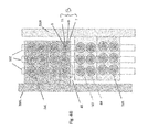
In an embodiment, the NAND string 180 illustrated in FIGS. 2A-4B may be formed with a vertical channel. In one aspect, the vertical channel 1 has a solid, rod shape as shown in FIGS. 2A, 2B, 3B, 3A and 4B. In this aspect, the entire channel comprises a semiconductor material. In another aspect, the vertical channel has a hollow cylinder shape as shown in FIG. 4A. In this aspect, the vertical channel includes a non-semiconductor core 2 surrounded by a semiconductor channel 1 shell. The core may be unfilled or filled with an insulating material, such as silicon oxide or silicon nitride.
In some embodiments, the monolithic three dimensional NAND string 180 comprises a semiconductor channel 1 having at least one end portion extending substantially perpendicular to a major surface 100 a of a substrate 100, as shown in FIGS. 2A, 2D, 3A and 3B. For example, the semiconductor channel 1 may have a pillar shape and the entire pillar-shaped semiconductor channel extends substantially perpendicularly to the major surface 100 a of the substrate 100. In these embodiments, the source/drain electrodes of the device can include a lower electrode 102 (e.g., a heavily doped semiconductor region source electrode in the major surface 100 a of a semiconductor substrate 100) provided below the semiconductor channel 1 (optionally in contact with a doped source region 103), and an upper electrode 202 (e.g., bit line) formed over the doped drain region 203 in the semiconductor channel 1, as shown in FIG. 2A. The lower electrode 102 contacts a metal interconnect outside of the view shown in FIGS. 2A and 3A or contacts metal wires of circuitry under the array. Thus, the drain/bit line electrode 202 contacts the pillar-shaped semiconductor channel 1 (via the drain region 203) from above, and the source electrode 102 contacts the pillar-shaped semiconductor channel 1 from below (e.g., via source region 103). For example, the device shown in FIGS. 2A and 2D contains two levels of landing pads 25, which divide the channel and the stack into three portions: lower portion of the stack 120L containing the lower portions 1 xa, 1 xb of the wings 1 a, 1 b; middle portion of the stack 120M containing the middle portions 1 ya, 1 yb of the wings 1 a, 1 b; and upper portion of the stack 120U containing the upper portions 1 za, 1 zb of the wings 1 a, 1 b.
Alternatively, as shown in FIG. 2B, the NAND string may have a U shape (also known as a “pipe” shape) with two vertical channel wing portions connected with a horizontal channel connecting the wing portions. In one aspect, the U shaped or pipe shaped channel may be solid, as in the solid rod shaped vertical channel NAND as shown in FIG. 2B. In another aspect, the U shaped or pipe shaped channel may be hollow cylinder shaped, (similar to the hollow cylinder pipe shaped vertical channel NAND as shown in FIG. 4A). The U-shaped pipe channel may be filled or unfilled. Separate front side and back side methods for fabricating both single vertical channel and U shaped channel NAND strings are taught in U.S. Pat. No. 8,187,936, hereby incorporated by reference in its entirety for teaching of the separate front and back side processing methods.
The two wing portions 1 a and 1 b of the U-shape semiconductor channel may extend substantially perpendicular to the major surface of the substrate, and a connecting portion 1 c of the U-shape semiconductor channel 1 connects the two wing portions 1 a, 1 b extends substantially perpendicular to the major surface of the substrate. The wing portions 1 a, 1 b of the channel 1 contain the built-in landing pads/resistors 25. For example, the device shown in FIGS. 2B and 2E contains two levels of landing pads 25, which divide the channel and the stack into three portions: lower portion of the stack 120L containing the lower portions 1 xa, 1 xb of the wings 1 a, 1 b; middle portion of the stack 120M containing the middle portions 1 ya, 1 yb of the wings 1 a, 1 b; and upper portion of the stack 120U containing the upper portions 1 za, 1 zb of the wings 1 a, 1 b.
In these embodiments, one of the source or drain electrodes 202 (e.g., bit line) contacts the first wing portion of the semiconductor channel from above, and another one of a source or drain electrodes (e.g., source line) 102 contacts the second wing portion of the semiconductor channel 1 from above. An optional body contact electrode 91 may be disposed over or in the substrate to provide body contact to the connecting portion of the semiconductor channel 1 from below. The NAND string's select or access transistors 16 are shown in FIGS. 2B and 2E. These transistors and their operation are described in U.S. Pat. No. 8,187,936, which is incorporated by reference for a teaching of the select transistors. The device of FIGS. 2B and 2E is described in more detail below with reference to the method of making the P-BiCS type vertical NAND, as shown in FIGS. 17A-17H.
The substrate 100 can be any semiconducting substrate known in the art, such as monocrystalline silicon, IV-IV compounds such as silicon-germanium or silicon-germanium-carbon, III-V compounds, II-VI compounds, epitaxial layers over such substrates, or any other semiconducting or non-semiconducting material, such as silicon oxide, glass, plastic, metal or ceramic substrate. The substrate 100 may include integrated circuits fabricated thereon, such as driver circuits for a memory device.
Any suitable semiconductor materials can be used for semiconductor channel 1, for example silicon, germanium, silicon germanium, indium antimonide, or other compound semiconductor materials, such as III-V or II-VI semiconductor materials. The semiconductor material may be amorphous, polycrystalline or single crystal. The semiconductor channel material may be formed by any suitable deposition methods. For example, in one embodiment, the semiconductor channel material is deposited by low pressure chemical vapor deposition (LPCVD). In some other embodiments, the semiconductor channel material may be a recyrstallized polycrystalline semiconductor material formed by recrystallizing an initially deposited amorphous semiconductor material.
The insulating fill material 2 in FIG. 4A may comprise any electrically insulating material, such as silicon oxide, silicon nitride, silicon oxynitride, or other insulating materials.
Each monolithic three dimensional NAND string 180 further comprises a plurality of control gate electrodes 3, as shown in FIGS. 2A, 2B, 3A, 3B and 4A-4B. The control gate electrodes 3 may comprise a portion having a strip shape extending substantially parallel to the major surface 100 a of the substrate 100. The plurality of control gate electrodes 3 comprise at least a first control gate electrode 3 a located in a first device level (e.g., device level A) and a second control gate electrode 3 b located in a second device level (e.g., device level B) located over the major surface 100 a of the substrate 100 and below the device level A, as shown in FIGS. 2A, 2B, 3A and 4A. The control gate material may comprise any one or more suitable conductive or semiconductor control gate material known in the art, such as doped polysilicon or a metal, such as tungsten, copper, aluminum, tantalum, titanium, cobalt, titanium nitride or alloys thereof.
Each channel 1 shown in FIGS. 2A-4B contains one or more landing pads/built-in resistors 25 described above. Preferably, each landing pad 25 is located in a vertical position of the channel between control gates 3 (i.e., having one control gate above and one control gate below). Thus, the landing pad is located between the first device level (e.g., level A) and the second device level (e.g., level B). A lower portion of the semiconductor channel (e.g., 84 x) located in the first device level contacts a bottom surface of the landing pad 25. A middle or upper portion (e.g., 84 y) of the semiconductor channel located in the second device level contacts a top surface of the same landing pad 25.
The landing pad 25 may extend horizontally beyond the memory hole 84 diameter or width to be located over and under adjacent control gates 3 inside the dielectric fill material 121 Thus, the landing pad 25 may extend into the insulating layer 121 between the first 3 a and the second 3 b control gate electrodes 3. The fill material 121 isolates the landing pad 25 from direct contact with the control gate electrodes 3. Alternatively, the landing pad 25 may be relatively thick and contact dummy control gate electrodes 3 d, as shown in FIGS. 17G and 17H. Dummy control gate electrodes 3 d (i.e., dummy word lines) are not connected to outside control circuitry and are not provided with a current or voltage during NAND operation.
A blocking dielectric 7 is located adjacent to and may be surrounded by the control gate(s) 3. The blocking dielectric 7 may comprise a continuous layer or a plurality of blocking dielectric segments located in contact with a respective one of the plurality of control gate electrodes 3. For example, a first dielectric segment 7 a located in device level A and a second dielectric segment 7 b located in device level B are in contact with control electrodes 3 a and 3 b, respectively, as shown in FIG. 4A. In some embodiments, at least a portion of each of the plurality of blocking dielectric segments 7 surrounds the top, bottom, and two edge portions of a control gate electrode 3 between two adjacent NAND strings, as shown in FIGS. 3A and 4A.
The NAND devices also comprise one or more charge storage regions 9 located between the channel 1 and the blocking dielectric 7. The charge storage regions 9 may comprise a continuous vertical charge storage layer adjacent to plural control gate electrodes 3, as shown in FIGS. 2A and 2B or the plurality of discrete charge storage regions 9 comprise at least a first discrete charge storage segment 9 a located in the device level A and a second discrete charge storage segment 9 b located in the device level B, as shown in FIG. 4A.
A tunnel dielectric 11 is located between the charge storage region(s) 9 and the semiconductor channel 1. The blocking dielectric 7 and the tunnel dielectric 11 may be independently selected from any one or more same or different electrically insulating materials, such as silicon oxide, silicon nitride, silicon oxynitride, or other insulating materials.
The charge storage region(s) 9 may comprise a conductive (e.g., metal or metal alloy such as titanium, platinum, ruthenium, titanium nitride, hafnium nitride, tantalum nitride, zirconium nitride, or a metal silicide such as titanium silicide, nickel silicide, cobalt silicide, or a combination thereof) or semiconductor (e.g., polysilicon) floating gate(s), conductive nanoparticles, or a charge storage dielectric layer or segment (e.g., silicon nitride or another dielectric). For example, in some embodiments, the charge storage regions comprise silicon nitride, where the silicon oxide blocking dielectric 7, the nitride charge storage region 9 and the silicon oxide tunnel dielectric 11 form oxide-nitride-oxide (ONO) memory film 13 of the NAND string shown in FIGS. 2A, 2B, 3A and 4A. Alternatively, the blocking dielectric may comprises a tri-layer ONO dielectric, such that the memory film 13 comprises ONO (11)-N (9)-O (7).
As shown in FIG. 4B, the tunnel dielectric 11 comprises a cylinder which surrounds the semiconductor channel 1, the charge storage region 9 comprises a cylinder which surrounds the tunnel dielectric, and the blocking dielectric 7 comprises a cylinder which surrounds the charge storage region. The first 3 a and the second 3 b control gate electrodes 3 surround the blocking dielectric in each NAND string.
The CVNAND configuration shown in FIGS. 3A-4B provides a denser memory design than the configurations shown in FIGS. 2A and 2B, respectively, for the following reasons. For example, as shown in FIG. 2A, each pillar NAND string 180 is separated from adjacent strings by a word line cut or trench 86. The bottom source select gate (SGS) device 16L in FIG. 2A requires a cut space or trench 86 between the lower select gate electrodes which are built from the bottom of the stack metal layer. Furthermore, the source line 102 formation process and p-well 300 contact requires additional space in the device of FIG. 2A.
Likewise, as shown in FIGS. 2B and 2E, each U-shaped P-BiCS NAND string 180 contains a dielectric 87 filled slit trench 86A between the select and control gates 3 and the wings or arms of the U-shaped channel 1 which extends between upper source line 102 and bit line 202. Furthermore, as shown in FIG. 2B, adjacent U-shaped NAND strings 180 are also separated by a word line cut or trench 86B not to lose active holes and to reduce word line R. The top view of the filled memory holes 84 (i.e., containing the NAND string channels 1 and a film 13 comprising tunnel dielectric, charge storage region and blocking dielectric) and the trenches 86 in vertical pillar and P-BiCS type devices is illustrated in FIG. 2C. The control gates are omitted from FIG. 2C for clarity and the supporting columns 88 which prevent the device levels from collapsing on each other during removal of sacrificial material are shown in the bottom of the figure. The trenches result in a higher than desired pitch between adjacent filled memory holes (e.g., a pitch of about 150 nm) and reduces the array efficiency by more than 50%.
The word line (i.e., control gate) trenches or cuts 86 in an array of vertical NAND strings may be eliminated to increase the device density and reduce the filled memory hole 84 pitch. Embodiments include monolithic three dimensional NAND strings and methods of making three dimensional NAND devices (e.g., CVNAND devices) having at least one 3×3 array of vertical NAND strings in which the control gate electrodes are continuous in the array and do not have an air gap or a dielectric filled trench 86 in the array. The NAND device is formed by first forming a lower select gate level having separated lower select gates, then forming plural memory device levels containing a plurality of NAND string portions, and then forming an upper select gate level over the memory device levels having separated upper select gates.
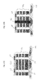
Embodiments of the compact vertical NAND (i.e., CVNAND) device are shown in FIGS. 3A, 3B, 3C, 4A and 4B. FIG. 3A schematically illustrates a side cross sectional view of the entire CVNAND device, including the lower 50 and upper 60 select gate device levels located below and above the memory device levels 70 shown in FIG. 4A. FIG. 3B schematically illustrates a side cross sectional view of the memory levels 70 and select gate device levels 50, 60 of one CVNAND array and FIG. 3C schematically illustrates the top view location of the filled memory holes 84 and supporting pillars 88. FIG. 4A illustrates a side cross sectional view of the memory device levels 70 (i.e., levels containing the control gate electrodes/word lines) in one NAND string array. FIG. 4B schematically illustrates the top cross sectional view of the relationship between the continuous control gate electrodes 3 and the filled memory holes 84 in each array block.
As shown in FIGS. 3A, 4A and 4B the first control gate electrode 3 a and the second control gate electrode 3 b are continuous in the array, such that these electrodes do not have an air gap or a dielectric filled trench in the array. As shown in FIG. 4B, the control gate electrodes 3 when viewed from the top comprise a “mesh” which is continuous except for the memory holes 84 which are completed filled with the channel 1, an optionally the tunnel dielectric 11, charge storage region 9, blocking dielectric 7 and optional insulating fill 2. In other words, the control gate electrodes 3 may be considered to be a mesh in which all openings are filled
FIG. 4B shows two control gate electrodes 3 aL and 3 aR (i.e., left and right electrodes) located in the first device level A. Each electrode forms a continuous mesh around an exemplary 4×3 array of filled memory holes 84. Each electrode 3 aL and 3 aR contacts a respective word line 200L and 200R of an array block. An array block includes plural arrays (e.g., plural 4×3 arrays) which are connected by their respective control gate electrodes (e.g., 3 aL) to a common word line (e.g., 200L). Only one array is shown as being connected to each word line via a respective control gate electrode in FIG. 4B for clarity. However, it should be understood that the pattern shown in FIG. 4B repeats along the word lines. Thus, each array is located in a respective array block, where the left control gate electrode 3 aL in one block in device level A is separated from the right control gate electrode 3 aR in the same level A in an adjacent array block by an air gap (if the slit trench 81 is not filled) or a dielectric filled trench 81. The same configuration is used in the other memory levels shown in FIGS. 4A and 3A.
The CVNAND string's select or access transistors 16L, 16U are shown in FIGS. 3A, 3B, 5, 6 and 11. As shown in FIGS. 3A and 5A-5C, a lower select gate electrode 51 is located adjacent to a lower portion 1L of the pillar-shaped semiconductor channel 1 below the control gate electrodes 3 (e.g., 3 a, 3 b) in the lower select gate electrode level 50. Level 50 may be a source select gate level and electrode 51 may be a source side select gate electrode. Each lower select gate electrode 51 is separated from adjacent lower select gate electrodes 51 in the array in level 50 by an air gap or a dielectric filled trench 53.
Furthermore, as shown in FIGS. 3A and 11A-C, an upper select gate electrode 61 is located adjacent to an upper portion 1U of the pillar-shaped semiconductor channel 1 above the first 3 a and the second 3 b control gate electrodes. Electrode 61 may comprise a drain side select gate electrode located in the drain upper select gate level 60. Each upper select gate electrode 61 is separated from adjacent upper select gate electrodes 61 in the array in level 60 by an air gap or a dielectric filled trench 63.
In one non-limiting embodiment, each semiconductor channel 1 comprises a first portion 1U adjacent to the upper select gate electrode 61, a second portion 1L adjacent to the lower select gate electrode 51, a third (i.e., middle or memory) portion 1M located at least in the first (A) and the second (B) device levels between the first and the second portions, and an optional, additional landing pad portion 55 located between the second 1L and the third 1M channel 1 portions.
In one embodiment shown in FIG. 3B, the third (middle) portion 1M of the channel 1 has a larger diameter or width than the first (upper) 1U and the second (lower) 1 L channel 1 portions because these three portions are formed in separate process steps as described below. The thinner upper 1U and lower 1L channel 1 portions allow the space for the air gap or a dielectric filled trench 53, 63 to be added between adjacent upper 61 and lower 51 select gates in respective levels 60 and 50. In contrast, since the control gates 3 are continuous and do not require air gap or trench adjacent to the middle (memory) portions 1M of the channel 1, the channel portions 1M may be thicker than channel portions 1U and 1L.
Finally, as shown in FIGS. 3A, 3B, 5 and 6 and as will be explained in more detail below, the channel 1 may optionally contain additional landing pad portions 55 between the lower select gate level 50 and the memory levels 70 and between the memory level 70 and the upper select gate level 60. The landing pad portion has a larger diameter or width than the second 1L and the third 1M portions of the channel 1.
FIGS. 5A-5C illustrate a lower select gate level 50 of the CVNAND device. FIG. 5C shows a top view and FIGS. 5A and 5B illustrate side cross sectional views along lines A-A′ and B-B′ in FIG. 5C. The lower select gate level 50 is located over the substrate 100. The lower select gate level 50 includes the lower portions 1L of the plurality of semiconductor channels 1 (containing source regions 103 on the bottom), and a plurality of lower source electrodes 102. Each lower source electrode is electrically connected to each of the plurality of lower portions 1L of the semiconductor channels through a respective source region 103. Level 50 also includes the plurality of lower select gate electrodes 51, located adjacent to a gate dielectric 54 contacting the lower portion 1L of each semiconductor channel 1. The channel 1L, gate dielectric 54 and select gate 51 form the lower (source) select transistor 16L of each NAND string. Strip shaped lower select gate lines 52 connect the select gates 51 in rows to input/outputs (not shown), as shown in FIGS. 5B and 5C. Level 50 is formed before the layers of the memory level 70 are formed over level 50 to allow the select gates 50 to be separated.
FIGS. 6A-6D illustrate steps in forming this level 50 shown in FIG. 5A. As shown in FIG. 6A, the lower portions 1L of the channel 1 may be formed by etching a silicon substrate 100 to form silicon pillars 1L using any suitable lithography and etching technique. Alternatively, pillars 1L may be grown in openings in a mask located over the substrate 100. In this case, the select gate device level 50 is lifted up over the substrate 100 surface 100 a, so that the select transistors 16L have polysilicon channels 1L and CMOS devices may be formed in single crystal silicon substrate 100 under the NAND array. This option is less preferred.
This is followed by oxidizing the pillars 1L to form a silicon oxide gate dielectric 54 on pillar sidewall(s) and on exposed portion of substrate 100 surface 100 a. Alternatively, the gate dielectric may be deposited on the pillars 1L and the surface 100A of the substrate 100 by CVD or other suitable methods. In this case, the dielectric 54 may comprise materials other than silicon oxide.
Finally, the upper surface 100A of the substrate 100 is doped (e.g., by ion implantation) to form the source regions 103 and the source electrode 102 (i.e., buried doped source line in substrate 100). The buried source line 102 in the substrate 100 is made by a high dose implant. Alternatively, an optional a buried metal mesh (e.g., tungsten, etc.) may be provided in addition to or instead of the buried implanted lines 102 as the source electrode(s). Source regions 103 may be formed by angled ion implantation (e.g., phosphorus or arsenic implant into a p-type silicon substrate) into the base of the pillars 1L. The implantation may be conducted before or after the dielectric 54 formation or after the select gate 51 formation as it is described below.
Next, as shown in FIG. 6B, during a step of forming the lower select gate level 50, each lower select gate electrode 51 is separated from adjacent lower select gate electrodes in the array by an air gap or a dielectric filled trench 53. This may be done by forming the select gate 51 layer over the dielectric 54 covered lower portions 1L of the channel 1 followed by anisotripically etching the select gate layer to leave discreet, separated sidewall spacer shaped select gates 51 on the gate dielectric 54 covered lower portions 1L of the channel. The space between the spacer gates 51 may be left as an air gap or filled with an dielectric fill 53. Alternatively, select gates 51 may be formed by depositing a conductive layer and patterning it by lithography and etching into discreet gates 51. If desired, portions of the gates 51 of transistors 16L may be silicided.
The select gate lines 52 are then formed to connect the discreet select gates into rows. The lines 52 may be formed by depositing one or more conductive layers and then performing lithography and etching to form the strip shaped lines 52. The lines 52 are separated from each other in the A-A direction but not in the B-B direction in FIG. 5C.
Then, as shown in FIGS. 6C-6D, the optional semiconductor landing pad 55 may epitaxially grown over each lower portion 1L of the plurality of semiconductor channels 1 exposed in the dielectric filled trenches 53 in the lower select gate level 50, such that the landing pad has a larger width or diameter than an underlying lower portion of the channel.
The landing pad 55 formation may comprise epitaxially growing a “mushroom head” shaped overgrown silicon 56 on exposed portions 1L of the channels 1. This silicon overgrowth 56 is then covered by an insulating gap fill layer (e.g., silicon oxide or nitride). The silicon mushroom head 56 and the gap fill layer are then planarized (e.g., by CMP) to form planar landing pads 55 on each pillar 1L separated by an insulating gap fill 57, as shown in FIG. 6D.
FIGS. 7-10 illustrate a method of making the lower portion of the memory device levels 70 of FIGS. 4A and 3A after the step of forming a lower select gate level 50 according to an embodiment of the invention. The memory device levels 70 comprise a plurality of NAND string portions.
Referring to FIG. 7, a stack 120 of alternating layers 121 (121 a, 121 b, etc.) and 132 (132 a, 132 b etc.) is formed over the completed lower select gate device level 50 which is located over major surface of the substrate 100. Layers 121, 132 may be deposited over the substrate by any suitable deposition method, such as sputtering, CVD, PECVD, MBE, etc. The layers 121, 132 may be 6 to 100 nm thick. The stack 120 may be covered with an optional cap layer of insulating material 200 different from materials 121 and 132.
In this embodiment, the first layers 121 comprise an electrically insulating material, such as silicon oxide, silicon nitride, high-k dielectric (e.g., organic or inorganic metal oxide), etc. The second layers 132 are sacrificial layers. Any sacrificial material that can be selectively etched compared to material 121 may be used for layers 132, such as conductive or insulating or semiconducting material. For example, the sacrificial material for layers 132 may be silicon nitride when material of layers 121 is silicon oxide.
The deposition of layers 121, 132 is followed by etching the stack 120 to form a plurality of memory holes 84. An at least a 3×3, such as an at least 6×6 array of memory holes 84 may be formed in locations where vertical channels of NAND strings will be subsequently formed.
The middle semiconductor channel 1 portions 1M are then formed on the landing pads 55 exposed in the memory holes 84. The channel portions 1M may be filled with insulating fill 2 (as shown in FIG. 4A) or may comprise a solid rod (as shown in FIGS. 3A and 7).
Preferably, the channel 1 portions 1M material comprises lightly doped p-type or n-type (i.e., doping below 1017 cm−3) silicon material (e.g., polysilicon). An n-channel device is preferred since it is easily connected with n+ junctions (i.e., source 103 and drain 203 n+ doped regions having a doping concentration between 1017 cm−3 and 1021 cm−3). However, a p-channel device may also be used. Other semiconductor materials (e.g., SiGe, SiC, Ge, III-V, II-VI, etc.) may also be used.
The semiconductor channel 1 may be formed by any desired methods. For example, the semiconductor channel material 1 may be formed by depositing semiconductor (e.g., polysilicon) material in the holes 84 and over the stack 120 (e.g., by CVD), followed by a step of removing the upper portion of the deposited semiconductor layer by chemical mechanical polishing (CMP) or etchback using top surface of the stack 120 as a polish stop or etch stop.
In some embodiments, a single crystal silicon or polysilicon vertical channel 1 may be formed by metal induced crystallization (“MIC”, also referred to as metal induced lateral crystallization) without a separate masking step. The MIC method provides full channel crystallization due to lateral confinement of the channel material in the hole 84.
In the MIC method, an amorphous or small grain polysilicon semiconductor (e.g., silicon) layer can be first formed in the holes 84 and over the stack 120, followed by forming a nucleation promoter layer over the semiconductor layer. The nucleation promoter layer may be a continuous layer or a plurality of discontinuous regions. The nucleation promoter layer may comprise any desired polysilicon nucleation promoter materials, for example but not limited to nucleation promoter materials such as Ge, Ni, Pd, Al or a combination thereof.
The amorphous or small grain semiconductor layer can then be converted to a large grain polycrystalline or single crystalline semiconductor layer by recrystallizing the amorphous or small grain polycrystalline semiconductor. The recrystallization may be conducted by a low temperature (e.g., 300 to 600 C) anneal.
The upper portion of the polycrystalline semiconductor layer and the nucleation promoter layer can then be removed by CMP or etchback using top surface of the stack 120 as a stop, resulting in the structure as shown in FIG. 7. The removal may be conducted by selectively wet etching the remaining nucleation promoter layer and any formed silicide in the top of layer following by CMP of the top of silicon layer using the top of the stack 120 as a stop.
Following formation of the channel 1 portions 1M, at least one slit trench 81 (also shown in FIG. 4B) is formed in the stack 120. The openings 81, 84 may be formed by forming a mask (e.g., a photoresist mask) by photolithography followed by etching unmasked areas. The slit trench opening 81 may be in the shape of a cut traversing more than one NAND string as illustrated in FIG. 4B. The slit trenches 81 allow back side access to the vertical NAND strings located in memory holes 84 for the control gate 3 formation in the “gate last” process.
Next, as shown in FIG. 8, the sacrificial material 132 is selectively etched compared to the first layer 121 material to form recesses 62. The recesses 62 may be formed by selective, isotropic wet or dry etching which selectively etches the sacrificial material 132 compared to the first layer insulating material 121 through the slit trenches 81. The recess 62 extends to the channel 1 portions 1M. Preferably, the entire layers of first sacrificial material 132 between the first layers 121 are removed up to the channel 1 portions 1M.
The memory film 13 is then formed in the recesses 62 as shown in FIG. 9. This includes forming a tunnel dielectric 11 in the recesses over the channel portions 1M located in the memory openings 84, forming a charge storage region 9 over the tunnel dielectric, and forming a blocking dielectric 7 over the charge storage region in the recesses 62. The blocking dielectric 7 may comprise a silicon oxide layer deposited by conformal atomic layer deposition (ALD) or chemical vapor deposition (CVD). Other high-k dielectric materials, such as hafnium oxide, may be used instead or in addition to silicon oxide. Dielectric 7 may have a thickness of 6 to 20 nm. The charge storage region 9 may comprise a silicon nitride layer deposited by any suitable method, such as ALD, CVD, etc., and have a thickness of 3 to 20 nm. The tunnel dielectric may comprise a relatively thin insulating layer (e.g., 4 to 10 nm thick) of silicon oxide or other suitable material, such as oxynitride, oxide and nitride multi layer stacks, or a high-k dielectric (e.g., hafnium oxide). The tunnel dielectric may be deposited by any suitable method, such as ALD, CVD, etc. Alternatively, the tunnel dielectric may be formed by thermally oxidizing the exposed sidewalls of the middle portions 1M of the channel 1 exposed in the recesses 62.
The control gates 3 are then formed on the blocking dielectric in the remaining portions of the recesses 62 through the slit trench(es) 81, as shown in FIG. 10. The control gates 3 are preferably metal or metal alloy gates, such as tungsten gates, formed by MOCVD or other suitable methods. Finally, if desired, the slit trenches 81 between array blocks may be filled with a dielectric fill material or they may be left unfilled as air gap trenches. This completes the lower portion of the memory device levels 70.
Then, a landing pad/built-in resistor 25 is formed over the channel 1M, as will be described below with respect to FIG. 16A. The process of FIGS. 7-10 is repeated again one or more times to form one or more upper portions of the memory levels 70 over the completed lower portion of the memory levels 70, as shown in FIG. 16B, and described in more detail below.
FIGS. 11A-11C illustrate the upper select gate level 60 of the device. FIG. 11C shows a top cross sectional view (along lines A-A and B-B in FIGS. 11A and 11B, respectively, with bit line 202 not shown) and FIGS. 11A and 11B illustrate side cross sectional views along lines A-A′ and B-B′ in FIG. 11C. The upper select gate level 60 is formed over the plurality of memory device levels 70, preferably after levels 70 are completed and preferably without using the stack 120 layers. The upper select gate level 60 comprises upper portions 1U of the plurality of semiconductor channels 1, and a plurality of upper drain electrodes (e.g., bit lines) 202. Each upper source or drain electrode 202 is electrically connected to each of the plurality of upper portions 1U of the semiconductor channels via the drain regions 203. Level 60 also includes a plurality of upper select gate electrodes 61. Each upper select gate electrode 61 is located adjacent to a gate dielectric 64 contacting the upper portion 1U of each semiconductor channel 1. The channel portion 1U, gate dielectric 64 and select gate 61 form the upper (drain) select transistor 16U of each NAND string. The upper select gate lines 66 separated from each other by insulating fill 63 connect the select gates 61 in rows.
The upper select gate level 60 may be formed in the same manner as the lower select gate level 50, except as follows. First, the upper portions 1U (i.e., the channels of the upper select gate transistors 16U) of the channels 1 are grown on the respective middle portions 1M of the channels. Thus, portion 1U may comprise polycrystalline semiconductor (e.g., polysilicon) or recrystallized, nearly single crystal silicon (e.g., recrystallized by the MIC process).
Second, rather than forming landing pads 55, the tops of the pillars 1U are doped with a dopant of the opposite conductivity type (e.g., n-type) than that of the channel 1 portion 1U (e.g., p-type) to form drain regions 203. This may be performed by ion implanting P or As into exposed portions of silicon pillars 1U. Third, as shown in FIG. 11B, the bit lines 202 are formed by a damascene process in rail shaped trenches in a dielectric layer 204 or by forming the dielectric layer 204 around bit line 202 rails. Otherwise, the upper select gate electrodes 61 may be formed by a sidewall spacer process on gate dielectric 64 covered silicon channels 1L of the upper select gate transistors 16U in the same matter as the lower select gate electrodes 51. If desired, portions of the gates 61 and/or the drain 203 of transistors 16U may be silicided.
FIGS. 12A and 12B illustrate exemplary dimensions (in nanometers) of the select transistors 16 and elements of levels 50 and 60, respectively, in units of nanometers. The above configuration provides a dense array for larger block sizes. The CVNAND scales below 5 nm effective half pitch (F/n), where F is the minimum feature size and n is the number of device levels.
The above described NAND device may be programmed and read by conventional NAND techniques. However, since the select gates for each NAND string are separated, the erase operation of the above device may be advantageously performed by a gate induced drain leakage (GIDL) process through the lower select gate source transistor 16L in the lower select gate device level 50. The effective GIDL erase allows erasing of very tall stacks by optimizing the bottom SGS transistor 16L with respect to GIDL current (during erase) and off/leakage currents (during inhibit). This also provides an effective erase from source line 102 side only, which allows optimization of off current and leakage current (during inhibit and read) for top SGD transistor 16U. This allows the device to open up an inhibit window and reduce read current leakage for non selected blocks. It is believed that sub block erase could become effective compared to prior art three dimensional NAND.
FIGS. 13A and 13B are side cross sectional views of a NAND memory device of embodiments of the invention. The devices shown in FIGS. 13A and 13B are similar to the device shown in FIG. 3A above, except that the devices shown in FIGS. 13A and 13B contain a local interconnect (source contact) 302. The local interconnect 302 may extend below the array in the embodiment of FIG. 13A (e.g., the local interconnect may extend in and out of the page under the array in the view of FIG. 13A). Alternatively, the local interconnect 302 may extend in the slit trenches 81 in the embodiment of FIG. 13B. The local interconnect 302 may comprise any suitable conductive material, such as tungsten, aluminum, copper, etc.
In the embodiment of FIG. 13B, the local interconnect 302 comprises a vertical pillar which electrically contacts the lower electrode 102 (e.g., the heavily doped semiconductor region source electrode in the major surface of the semiconductor substrate 100 or another electrode located over the substrate). The upper portion of the local interconnect 302 is in electrical contact with a source line.
In the present embodiment, the slit trenches 81 and the local interconnect 302 extend through the memory device levels 70 and through the dielectric trench fill material 53 to an exposed upper surface of the lower electrode 102. Preferably, the sidewalls of the slit trenches 81 are coated with an insulating layer 304, such as silicon oxide (see FIGS. 14D and 14E), and the local interconnect is formed in the middle of the slit trenches 81 between the insulating layer 304 portions.
As shown in FIG. 13B, the width of the array of vertical NAND strings is defined by the space between adjacent trenches 81, at least one or more of which can be filled with the local interconnect 302. The local interconnect 302 may contact a common lower electrode 102 of adjacent arrays of strings to provide source side erase for the strings in plural arrays of NAND strings at the same time.
The local interconnect may be formed by etching the trenches 81 as described above all the way to the lower electrode 102, forming the insulating layer 304 in the trenches 81 and filling the remaining central space in the trenches with the conductive material of the local interconnect 302. The portions of the conductive layer of the local interconnect 302 and/or insulating layer 304 which extends out of the trenches 81 may be removed by planarization, such as CMP. In the alternative embodiment of FIG. 13A, the local interconnect is formed under the array prior to formation of the array.
FIG. 14A is a top cross sectional view of the prior art BiCS NAND device shown in FIGS. 1B and 2B. FIGS. 14B and 14C are a top cross sectional views of the CVNAND memory devices according to embodiments of the invention.
As shown in FIG. 14B, the filled memory holes 84 (i.e., holes 84 containing the pillar channel 1 and memory film 13) are arranged in a square or rectangular layout with the memory holes located at corners of an imaginary rectangle or square, similar to the BiCS layout in FIG. 14A. The upper select gates 61, bit lines 202 and local interconnect 302 extending to the lower electrode 102 are also shown in FIG. 14B.
FIG. 14C illustrates an alternative embodiment in which the filled memory holes 84 (i.e., the NAND string channel 1 and memory film 13) are arranged in a substantially hexagonal pattern. This pattern comprises a repeating unit pattern of seven filled memory holes 84 having a central hole 84 surrounded by six other holes 84 arranged in a hexagonal layout around the central hole 84. In other words a central semiconductor channel 1 and memory film 13 unit is surrounded by six other semiconductor channel and memory film units arranged in a hexagonal layout around the central semiconductor channel and memory film unit. The hexagonal pattern has three axes of symmetry, in the same plane, about a point the array. The three axes are separated by substantially 60 degrees from one another. Hence, the memory holes 84 are arranged on a hexagonal grid which is also known as hexagonal tiling, bitruncated hexagonal tiling, or omnitruncated hexagonal tiling. Advantageously, hexagonal packing of the takes only about 87% of the area typically used by the same number of cells using standard rectangular layout shown in FIG. 14A.
The memory holes 84 in the hexagonally tiled configuration of FIG. 14C are staggered along each select gate 51, 61 when viewed from the top. The hexagonally tiled configuration of FIG. 14C provides a relaxed layout (i.e., larger pitch) for the select gates 51, 61 compared to the layout of FIGS. 14A and 14B. However, the density of the array with the hexagonally tiled configuration of FIG. 14C can be increased compared to the layout of FIGS. 14A and 14B, with the bit line 202 pitch reduced by a factor of 2 compared to the one in the layout of FIGS. 14A and 14B.
FIGS. 14D and 14E are respective side cross sectional views along lines A-A′ and B-B′ in FIG. 14C of the CVNAND memory device with the hexagonally tiled memory hole 84 configuration. Line A-A′ is a diagonal line through filled memory holes 84 located on bit lines 1, 3, 4 and 5. Line B-B is a line along bit line 5. In the example shown in FIG. 14C, there are six bit lines (BL1, BL2, BL3, BL4, BL5 and BL6) and three select gates 61 which form a 6×3 hexagonally tiled array of eighteen NAND strings between adjacent local interconnects 302. Arrays having a configuration other than 6×3 may also be used as desired.
FIGS. 14D and 14E also illustrate the connector lines 351, 361 for the respective lower select gates 51 and upper select gates 61 of the respective SGS 16L and SGD 16U select transistors. The lines 351, 361 may comprise any suitable conductor, such as tungsten, and may connect the select gates to the driver/control circuits (not shown).
As shown in FIG. 14D, the diameter of each memory hole 84 is labeled d1 and the distance between adjacent memory holes 84 (along the diagonal line A-A′ in FIG. 14C) is labeled d2. The distance between adjacent memory holes 84 (along a given bit line, BL5, along the vertical line B-B′ in FIG. 14C) is √3*(d1+d2)−d1.
FIGS. 15A to 15H are schematic side cross sectional views of steps in the method of making the vertical pillar shaped channel type NAND memory device with one or more landing pads 25 shown in FIG. 2A. In this method, a lower portion of the channel 1 is formed in the respective lower portion of the memory opening 84 in the lower portion of the stack. This is followed by forming the landing pad 25, forming at least one additional portion of the stack, forming at least one additional portion of the memory opening to expose the landing pad 25 and forming at least one additional portion of the channel 1 in the memory opening in contact with the landing pad 25.
The method begins by forming the lower electrode 102, such as by implanting a heavily doped diffusion region 102 in the upper surface 100 a of the substrate 100. For example, region 102 may comprise an n+ doped region in a p-type substrate 100, as shown in FIG. 15A. The conductivity types may be reversed if desired. Diffusion (doped) region 102 serves as a common source line of the lower select gate transistor to be formed in region 16LS containing a sacrificial layer 1325 (e.g. a SiN layer).
The lower portion of the memory stack 120L is then formed over the upper surface 100 a of the substrate 100. The stack contains alternating insulating layers 121, such as silicon oxide layers, and sacrificial layers 132, such as silicon nitride layers. A hard mask 27 is formed over the lower portion of the stack. The hard mask is patterned (e.g., by lithography) and is used as a mask to etch the lower portions of the memory openings 84 x in the lower portion of the stack 120L. The etching may comprise an RIE or another suitable etching. The hard mask 27 may then be removed or retained in the device. Alternatively, the hard mask is consumed during the etching process.
Then, the lower portion of the channels 1 x are formed in the lower portion of the memory openings 84 x, as shown in FIG. 15B. The lower portion of the channels 1 x may have a pipe shape as illustrated in FIG. 15B, the center of which may be filled with an insulating material 2. Alternatively, the memory openings 84 x may be completely filled with semiconducting material to form the lower portions of the channels 1 x. Any suitable formation method may be used, such as the method described above with respect to FIGS. 7-10.
The landing pad 25 is then formed on top of the lower portion of the channel 1 x, as shown in FIG. 15C. The landing pad 25 may be formed using any suitable method, such as the method described above for forming the additional landing pad 25 with respect to FIGS. 6C-6D.
For example, a semiconductor landing pad 25 may be epitaxially grown over the each lower portion of the channels 1 x exposed in the lower portion of the stack 120L, such that the landing pad has a larger width or diameter than an underlying lower portion of the channel 1 x. The landing pad 25 formation may comprise epitaxially growing a “mushroom head” shaped overgrown silicon on exposed lower portions of the channels 1 x. This silicon overgrowth is then covered by an insulating gap fill layer (e.g., silicon oxide or nitride). The silicon mushroom head and the gap fill layer are then planarized (e.g., by CMP) to form planar landing pads 25 on each portion of the channel 1 x separated by an insulating gap fill 521, as shown in FIG. 15C.
Alternatively, the landing pads 25 may be formed by depositing a conductive or a doped semiconductor layer over the lower portion of the stack 120L and then patterning the layer by lithography and etching to leave landing pads 25 having a larger width than that of the lower channel portion 1 x. If the landing pads 25 are made of a doped semiconductor, then the landing pads 25 preferably have a higher doping concentration than the channel 1.
As illustrated in FIG. 15D, a lower portion of the word line cut or trench 86 x may then be formed in the lower portion of the stack 120L. This cut or trench 86 x may be formed by photolithography and etching. The cut or trench 86 x may be filled with a sacrificial or insulating material to protect it during subsequent processing. Alternatively, the portion of the cut or trench 86 x is omitted and the entire cut or trench 86 is formed in a single etching step after all of the memory levels are completed. This completes the lower memory level of the NAND device.
Then, the above process may be repeated one or more times to form one or more additional memory levels over the lower memory level. As shown in FIG. 15E, the process of FIGS. 15A-15D is repeated for the middle portion of the stack 120M. Specifically, the middle portion of the stack 120M is formed over the landing pads 25 and the lower portion of the stack 120L containing the lower portions of the channels 1 x. Another hard mask is formed over the middle portion of the stack 120M, and the middle portions of the memory openings 84 y are etched into the middle portion of the stack 120M to expose the landing pads 25, as shown in FIG. 15E. It should be noted that the lower 84 x and middle 84 y portions of each memory opening 84 may be partially or completely misaligned with each other, as long the landing pads 25 are exposed in respective middle portions of the memory openings 84 y.
Then, the middle portion of the channels 1 y are formed in the middle portions of the memory openings 84 y, as shown in FIG. 15E. The landing pad 25 is then formed on top of the middle portion of the channel 1 y. The landing pad 25 may be formed using any suitable method, such as the method described above. As illustrated in FIG. 15F, a middle portion of the word line cut or trench 86 y may then be formed in the middle portion of the stack 120M. This cut or trench 86 y may be formed by photolithography and etching, and optionally filled with a sacrificial or insulating material. This completes the middle memory levels.
If desired, one or more additional middle or upper portions of the memory levels are then formed over the middle memory levels. As shown in FIGS. 15E and 15F, the process of FIGS. 15A-15D is repeated for the upper portion of the stack 120U. Specifically, the upper portion of the stack 120U is formed over the landing pads 25 and the middle portion of the stack 120M containing the middle portions of the channels 1 y. Another hard mask is formed over the upper portion of the stack 120U, and the upper portions of the memory openings 84 z are etched into the upper portion of the stack 120U to expose the landing pads 25, as shown in FIG. 15E. It should be noted that the middle 84 y and upper 84 z portions of each memory opening 84 may be partially or completely misaligned with each other, as long the landing pads 25 are exposed in respective upper portions of the memory openings 84 z.
Then, the upper portion of the channels 1 z are formed in the upper portions of the memory openings 84 z, as shown in FIG. 15E. The landing pad 25 is then formed on top of the upper portion of the channel 1 z. The landing pad 25 may be formed using any suitable method, such as the method described above. The upper select transistor region 16US may also be formed during this step or during a separate step.
As illustrated in FIG. 15F, an upper portion of the word line cut or trench 86 z is then formed in the upper portion of the stack 120U. This cut or trench 86 z may be formed by photolithography and etching. If the cut or trench portions 86 x, 86 y were filled with a sacrificial material, then the sacrificial material is removed at this time and the cut or trench may be subsequently refilled with an insulating material. Alternatively, the entire cut or trench 86 is formed in a single etching step at this time through the entire stack 120 as illustrated in FIGS. 15I-15J.
The memory films and the control gate electrodes are then formed in the entire stack 120 using a back side process (similar to the process shown in FIGS. 8-10). First, as shown in FIG. 15G, the sacrificial material layers 132 (such as the silicon nitride layers), are removed from the stack 120 through the cut or trench 86 using a selective wet etch to leave recesses 62 between the insulating layer 121 in the stack 120. The memory film 13 (e.g., an ONO film) is then formed on the surface of the recesses 62 through the cut or opening 86, as shown in FIG. 15H. The control gate electrodes 3, such as metal (e.g. W or Ti) and/or metal nitride, (e.g. WN or TiN) are then formed in the recesses 62 on the memory films 13 through the cut or opening 86, as shown in FIG. 15I.
In an alternative embodiment, the back side process shown in FIGS. 15F-15I is performed on each portion of the stack between the channel and landing pad formation steps rather than on the entire stack. In this alternative method, after the lower portion of the channels 1 x are formed in the lower stack portion 120L in FIG. 15B, the cut or trench 86 x is formed in the lower portion of the stack 120L and sacrificial material layers 132 are removed to leave recesses 62. The recesses are then filled with the memory films 13 and the control gate electrodes 3. The cut or trench 86 x may be filled with an insulating or sacrificial material and the landing pads 25 are then formed on the lower portion of the channels 1 x. The process then continues as shown in FIG. 15E.
Then, after the middle portion of the channels 1 y are formed in the middle stack portion 120M in FIG. 15E, the cut or trench 86 y is formed in the middle portion of the stack 120M and sacrificial material layers 132 are removed to leave recesses 62. The recesses are then filled with the memory films 13 and the control gate electrodes 3. The cut or trench 86 y may be filled with an insulating or sacrificial material and the landing pads 25 are then formed on the middle portion of the channels 1 y. The process then continues as shown in FIGS. 15E-15H.
Then, after the upper portion of the channels 1 z are formed in the upper stack portion 120U in FIG. 15H, the cut or trench 86 z is formed in the upper portion of the stack 120L and sacrificial material layers 132 are removed to leave recesses 62. The recesses are then filled with the memory films 13, the control gate electrodes 3 as well as the lower 16LG and upper 16UG select gate electrodes in the respective regions in 16LS and 16US to form the lower 16L and upper 16U select gate transistors. The cut or trench 86 z may be filled with an insulating material 87. This results in the device shown in FIG. 15J.
After the control gate electrodes 3 are formed, either by the method of FIGS. 15A-15J or by the alternative method described above, the bit line contact 202 is then formed in contact with the upper channel portion 1 z as shown in FIG. 2A or 15K to complete the pillar shaped channel vertical NAND with landing pads 25.
A similar method may be used to form the CVNAND of FIGS. 3A-14E, as shown in FIGS. 16A and 16B. As shown in FIG. 16A, the lower portion of the memory levels 70L is formed over the lower select gate level 50, which is formed using the methods shown in FIGS. 5A-6D. The lower portion of the memory levels 70L includes the lower portion of the memory stack 120L. A hard mask is formed over the lower portion of the stack. The hard mask is patterned (e.g., by lithography) and is used as a mask to etch the lower portions of the memory openings 84 x in the lower portion of the stack 120L. The etching may comprise an RIE or another suitable etching. The hard mask may then be removed or retained in the device. Alternatively, the hard mask is consumed during the etching process.
Then, the lower portions of the memory films 13 x and the channel 1 x are formed in the lower portions of the memory openings 84 x as shown in FIG. 16A. Any suitable formation method may be used, such as the method described above with respect to FIGS. 7-10 or the front side method described below with respect to FIGS. 17A-17H. The landing pad 25 is then formed on top of the lower portion of the channel 1 x. The landing pad 25 may be formed using any suitable method, such as the method described above. This completes the lower memory levels 70L of the NAND device.
Then, the above process may be repeated one or more times to form one or more additional memory levels 70U over the lower memory levels 70L. As shown in FIG. 16B, the process of FIG. 16A is repeated for the upper portion of the stack 120U. Specifically, the upper portion of the stack 120U is formed over the landing pads 25 and the lower portion of the stack 120L containing the lower portions of the channels 1 x. Another hard mask is formed over the upper portion of the stack 120U, and the upper portions of the memory openings 84 z are etched into the upper portion of the stack 120U to expose the landing pads 25. It should be noted that the lower 84 x and upper 84 z portions of each memory opening 84 may be partially or completely misaligned with each other, as long the landing pads 25 are exposed in respective upper portions of the memory openings 84 z.
Then, the upper portions of the memory films 13 z and the channel 1 z are formed in the upper portions of the memory openings 84 z as shown in FIG. 16B. The upper select transistor level 60 is then formed over the upper memory levels 70U using the method shown in FIGS. 11A-12B. A similar method to the one described in FIGS. 15A-15F and 16A-16B may be used to form other vertical NAND devices with landing pads, such as P-BiCS type devices.
FIGS. 17A through 17H illustrate another embodiment of making 3D vertical NAND devices. Specifically, FIGS. 17A-17H illustrate a method of overcoming misalignment of the memory holes in making NAND memory devices that have at least two memory stacks. In this embodiment method, lower portions of the memory openings 84 x are formed in the lower portion of the stack 120L. This is followed by filling the lower parts 84 s of the lower portions of the memory openings 84 x with a sacrificial material 31, and widening the remaining exposed top parts 84 t of the of the lower portions of the memory openings 84 x where the landing pad 25 will be subsequently formed. The widened part 84 t is then filled with a sacrificial material. Then, at least one additional portion of the stack 120U is formed over the lower portion of the stack 120L. At least one additional portion (e.g., the upper portions) of the memory openings 84 z are formed in the additional portion of the stack 120U to expose the sacrificial material in part 84 t of the lower portions of the memory openings 84 x. Then, the sacrificial material is removed from the entire opening 84 and the entire memory films 13 are formed in the memory openings 84 followed by forming the entire channels 1 and the landing pads 25 in the memory openings 84 in the same growth step (e.g., CVD growth step). Thus, in this method, the entire channel 1 (including landing pads 25 built into the channel 1) is formed in one step rather than in plural steps by using the sacrificial material to temporarily fill the memory opening portion 84 x.
As shown in FIG. 17A, a lower portion of the stack 120L of alternating layers 3, 121 is formed over the major surface 100 a of the substrate 100. Layers 3, 121 may be deposited over the substrate by any suitable deposition method, such as sputtering, CVD, PECVD, MBE, etc. The layers 3, 121 may be 6 to 100 nm thick. The substrate 100 may contain a sacrificial material region 29, such as a carbon or other suitable material.
The lower portion of the stack 120L may be covered with an optional cap layer of insulating material 123. The cap layer 123 is preferably thicker than layers 3, 121. For example, layer 123 may be 50-200 nm thick, such as 60-75 nm thick. The cap layer may comprise a silicon oxide layer, such as a silicon oxide layer formed by CVD using a TEOS precursor.
In this embodiment, the first layers 121 comprise an electrically insulating material, such as silicon oxide, silicon nitride, high-k dielectric (e.g., organic or inorganic metal oxide), etc. The second layers 3 comprise control gate material layers rather than the sacrificial material layers 132. The control gate material may comprise any one or more suitable conductive or semiconductor control gate material known in the art, such as doped polysilicon or a metal, such as tungsten, copper, aluminum, tantalum, titanium, cobalt, titanium nitride or alloys thereof. Thus, the stacks 120 in the pillar shaped channel, P-BiCS and/or CVNAND type devices may comprise alternating insulating 121 and sacrificial 132 layers (in the “back-side” process where the sacrificial material layers 132 are removed from the stack and the memory films 13 and control gate electrodes 3 are formed in place of layers 132 through the back side cut and recesses) or alternating insulating 121 and control gate 3 material layers (in a process where the control gate material layers are part of the initial stack and the memory film is formed through the memory holes 84).
The deposition of layers 3, 121 is followed by etching the lower stack portion 120L to form a plurality of lower portions of the memory openings 84 x. Then, as shown in FIG. 17B, the etch is continued into the sacrificial material region 29 to remove the sacrificial material and leave a connecting opening 30 which connects two adjacent lower portions of memory openings 84 x. The openings 84 x will eventually contain the two wing portions 1 a and 1 b of the U-shape semiconductor channel which extend substantially perpendicular to the major surface 100 a of the substrate 100, and the connecting opening 30 will contain the connecting portion 1 c of the U-shape semiconductor channel 1 which connects the two wing portions 1 a, 1 b and which extends substantially perpendicular (i.e., horizontally) to the major surface 100 a of the substrate 100.
As shown in FIG. 17C, the lower parts 84 s of the lower portions of the memory openings 84 x and the connecting opening 30 are filled with a sacrificial material 31. The sacrificial material may comprise any material which may be selectively etched compared to the materials of layers 3 and 121 and the material of the substrate 100. For example, for a silicon substrate 100, polysilicon control gate material layers 3 and silicon oxide layers 121, the sacrificial material 31 may comprise carbon, such as amorphous carbon. However, any other material may also be used.
Then, as shown in FIG. 17D, the remaining exposed top parts 84 t of the lower portions of the memory openings 84 x are widened such that the top parts 84 t have a larger width (e.g., larger diameter) than the bottom part 84 s. Preferably, the width (e.g., diameter) of the top part 84 t is the same as the intended width (e.g., diameter) of the landing pad 25 which will be subsequently formed in the top part 84 t. The widening may be performed by isotropically etching the cap layer 123 without substantially etching the sacrificial material 31 in the lower parts 84 s of the lower portions of the memory openings 84 x. The widened top parts 84 t are then refilled with the sacrificial material 31 a. Material 31 a may be the same or different from material 31. Material 31 a may be recessed to the top of the cap layer 123 by CMP or etchback.
Then, at least one additional portion of the stack (e.g., the upper portion of the stack) 120U is formed over the lower portion of the stack 120L, as shown in FIG. 17E. The additional portion of the stack 120U may also comprise alternating layers 3 and 121 described above. At least one additional portion (e.g., the upper portions) of the memory openings 84 z are formed in the additional portion of the stack 120U to expose the sacrificial material 31 a in the top part 84 t of the lower portions of the memory openings 84 x. If desired, the upper portions of the memory openings 84 z may be intentionally or unintentionally misaligned with the lower parts 84 s of the lower portions of the memory openings 84 x, as long as the upper portions of the memory openings 84 z expose a portion of the sacrificial material 31 a in the widened top parts 84 t of the lower portions of the memory openings 84 x.
As shown in FIG. 17F, the sacrificial material 31, 31 a is removed from the entire memory opening 84 (i.e., from both parts 84 s and 84 t). This may be performed by selectively etching away the sacrificial material in the memory opening. This forms the continuous memory openings 84 that extend through both the lower 120L and upper 120U portions of the stack 120. Each memory opening 84 includes portions 84 z and 84 x (which is made up of parts 84 s and 84 t) and the connecting opening 30.
The entire memory films 13 are then formed in the memory openings 84 in the entire stack, as shown in FIG. 17G. The memory films 13 are formed as hollow cylinders around the sidewalls of the openings 84.
This is followed by forming the entire U-shaped channels 1 and the landing pads 25 in the memory openings 84 in the same growth step inside the hollow memory film 13 cylinder. The two wing portions 1 a and 1 b of the U-shape semiconductor channel 1 extend substantially perpendicular to the major surface 100 a of the substrate 100 in portions 84 z, 84 x of the memory openings, and the connecting portion 1 c of the U-shape semiconductor channel 1 which connects the two wing portions 1 a, 1 b extends substantially perpendicular (i.e., horizontally) to the major surface 100 a of the substrate 100 in the connecting opening 30. In this embodiment, the landing pad 25 may be relatively thick and contact dummy control gates 3 d, as shown in FIG. 17G. Dummy control gates 3 d (i.e., dummy word lines) are not connected to outside control circuitry and are not provided with a current or voltage during NAND operation.
A slit trench or cut 86A is then formed between the select gates 3 and the wings or arms of the U-shaped channel 1, as shown in FIG. 17H. The slit trench or cut 86 may be etched until the etch stop layer 89 shown in FIG. 2B is reached during the etching. The trench or cut 86A may be filled with an insulating material 87, such as silicon nitride. The select gate transistors 16, the source line 102 and the bit line 202 are then formed above the device, as shown in FIG. 2B. Optionally, the substrate may include a body contact gate (e.g. bottom gate) 91 located adjacent to the connecting portion 1 c of the U-shape semiconductor channel 1, as shown in FIG. 2B.
If desired, the substrate may comprise a silicon on insulator type substrate containing one or more insulating layers 93 (e.g., silicon oxide/silicon nitride/silicon oxide stack) over a silicon wafer, as shown in FIG. 2B.
In another embodiment of the present invention, the vertical NAND devices described above (e.g., pillar shaped channel, P-BiCS or CVNAND type devices) may have a channel 1 comprising a mixed metal oxide semiconductor material. The devices with the mixed metal oxide semiconductor channel may include the landing pads 25 and be made by the sequential stack etching process described above. Alternatively, the vertical NAND devices with the oxide semiconductor channel may exclude the landing pad and have the entire memory holes etched in one step (e.g., such as the devices shown in FIGS. 1A and 1B).
Any suitable mixed metal oxide semiconductor material may be used. For example, the mixed metal oxide semiconductor comprises at least one first transition metal and at least one second metal selected from Group IIIA of the Periodic Table of Elements. The mixed metal oxide semiconductor my comprise one first transition metal from Group IIB (also known as Group 12) of the Periodic Table of Elements and two metals selected from Group IIIA (also known as Group 13) of the Periodic Table of Elements. Preferably, the mixed metal oxide comprises indium gallium zinc oxide (stoichiometric InGaZnO4 or non-stoichiometric material). Other mixed metal oxide semiconductors, such as zinc tin oxide (stoichiometric ZnSnO3 or non-stoichiometric material) or indium zinc oxide may also be used. The mixed metal oxide channels have a low leakage current and may be deposited at a low temperature (e.g., below 300 C, such as 100-270 C) into high aspect ratio memory holes 84 using atomic layer deposition (ALD) or other suitable methods.
FIGS. 18A to 18F are side cross sectional views of steps in the method of making the NAND memory device according to another embodiment. This embodiment includes a lower stack 120L of alternating control gate electrodes 3 and dielectric fill material 121 provided over a substrate 100. In an embodiment, the device includes an etch stop layer 89 located between a top surface of the substrate 100 and the stack 120L. As discussed in the previous embodiment, an optional sacrificial material region 29 which may be used to form a horizontal portion of a U-shaped channel 1 may also be provided.
Next, an optional slit trench may be etched to the etch stop layer 89 between the wings or arms of the U-shaped channel 1 and filled with a dielectric 87 as illustrated in FIG. 18B. Memory openings may then be etched through the stack 120 and the etch stop layer 89 to the sacrificial material region 29. The sacrificial material in sacrificial material region 29 is removed and the memory films (i.e. the blocking dielectric 7, charge storage regions 9, and tunnel dielectric 11) and channels 1 are formed in the memory openings as illustrated in FIG. 18C.
Next, as illustrated in FIG. 18D, a first insulating layer 121A, such as an oxide, is deposited over the stack 120L. A conducting or semiconducting current boosting layer 1801 is deposited over the insulating layer 121A. The current boosting layer 1801 may be a metal (e.g. tungsten or titanium), metal nitride, (e.g. WN or TiN), silicide or highly doped polysilicon (e.g., dopant concentration of at least 1018 cm−3). A second insulating layer 121B (e.g., silicon oxide) is then deposited over the current boosting layer 1801. As illustrated in FIG. 18E, a mask, such as a photoresist mask, may be applied to the surface of the second insulating layer 121B and patterned. Portions of the second insulating layer 121B, the current boosting layer 1801 and the first insulating layer 121A located over the memory holes may be removed by etching. A conducting or semiconducting material may then be deposited in the etched portion of the mask to form thick landing pads 25. That is, landing pads 25 may have a thickness greater than the thickness of the current boosting layer 1801 (e.g. 10-200% thicker, such as 50-100% thicker). The thick landing pads 25 are in electrical contact with both the current boosting layer 1801 and the channel 1. Alternatively, the current boosting layer 1801 may be thicker or the same thickness as the landing pads 25. Current flow in the NAND device can be boosted by applying a voltage to the current boosting layer 1801.
Next, as illustrated in FIG. 18F, the mask may be removed and a second, upper stack 120U of alternating control gate electrodes 3 and dielectric fill material 121 may be deposited over the second insulating layer 121B and the thick landing pads 25. The optional slit trench may then be extended through the upper stack 120U by etching to form a slit trench through the upper stack, the current boosting layer and the first and second insulating layers sandwiching the current boosting layer to the filled slit trench in the lower stack and filling the slit trench with a dielectric. After completing the filled slit trench, the select gates 16 may be formed over the upper stack 120U.
FIG. 18G illustrates another embodiment of a vertical NAND device with a current boosting layer 1801 and landing pad 25. Unlike the vertical NAND device illustrated in FIGS. 18A-18F which have a “U” shaped channel 1, the vertical NAND device illustrated in FIG. 18G has a single vertical pillar shaped channel. The vertical NAND device illustrated in FIG. 18G includes a lower select gate electrode 16L located proximal to the substrate 100 under the memory cells and the control gate electrodes, and an upper select gate electrode 16U located over the memory cells and the control gate electrodes. As in the previous embodiment, the vertical NAND device of this embodiment may have more than two stacks 120 of alternating control gate electrodes 3 and dielectric fill material 121. Further, if the vertical NAND device includes more than two stacks 120, then the device may have more than one current boosting layer 1801 (e.g. if the vertical NAND device has three stacks 120L, 120M, 120U, then the device may include a current boosting layer 1801 between the lower stack 120L and the middle stack 120M and a current boosting layer 1801 between the middle stack 120M and the upper stack 120L).
The current boosting layer 1801 is electrically connected to a voltage or current source and to the landing pad embedded in the semiconductor channel. In operation of the vertical NAND device, current or voltage may be applied to the current boosting layer 1801 during at least one of a read, program or erase steps of the vertical NAND device. In this manner, additional current or voltage may be provided to an interface region containing the landing pad between the upper and lower stacks 120U, 120L (and any intermediate stacks 120, if provided). The applied current or voltage assists in charge carrier (e.g., electron or hole) flow through the landing pad and the interface region. The additional current or voltage improves operation of the device (e.g. provides additional current flow between the select transistors 16L, 16U in each memory string), thereby increasing the reliability of operation by ensuring that sufficient current or voltage is available for proper operation of the stacks 120 of memory device levels in the NAND device.
FIGS. 19A to 19D illustrate a method of making the NAND memory device according to another embodiment. FIG. 19E is a schematic circuit diagram of the device of FIG. 19D. In this embodiment, at least one landing pad is located between a select gate electrode and an end control gate electrode in the stack. For example, the select gate electrode may comprise an upper select gate electrode and the end control gate electrode may comprise a top control gate electrode in the stack, and/or the select gate electrode may comprise a lower select gate electrode and the end control gate electrode may comprise a bottom control gate electrode in the stack.
As illustrated in FIG. 19A, this embodiment includes a stack 120 of alternating control gate electrodes 3 and dielectric fill material 121 provided over a substrate 100. In an embodiment, the substrate 100 may comprise a silicon on insulator type substrate containing one or more insulating layers 93 (e.g., silicon oxide/silicon nitride/silicon oxide stack) over a silicon wafer, as shown in FIG. 19A. Additionally, the substrate may include a bottom gate 91. To protect the bottom gate 91 during subsequent processing, an etch stop layer 89 may be provided between the bottom gate 91 and the stack 120.
In previous embodiments, landing pads 25 were provided between memory stacks 120. In this embodiment, the device includes at least one semiconductor or electrically conductive landing pad 2001 located between the stack(s) 120 of alternating control gate electrodes 3 and dielectric fill material 121 and at least one select gate electrode 16. Preferably, the landing pad 2001 is located between an upper select gate electrode 16 and an upper most control gate electrode 3 in the stack 120. Alternatively, or in addition the landing pad 2001 may be located between the lower select gate electrode (e.g., 16L in FIG. 18G) and the lower most control gate electrode 3 in a vertical NAND string having a single vertical pillar channel, such as the string shown in FIG. 18G. In an embodiment, a landing pad 2001 is provided between at least one of (1) the source select gate electrode 16S and the first and the second control gate electrodes 3 and (2) the drain select gate electrode 16D and the first and the second control gate electrodes 3. Preferably, landing pads 2001 are provided for both the source select transistor 2003 channel 1S and the drain select transistor 2005 channel 1D for embodiments with U-shaped channels as illustrated in FIGS. 19B-19E. For NAND strings with a vertical channel (e.g., such as the strings shown in FIGS. 2A and 3A), one landing pad 2001 is shown as being provided for the channel of the upper select gate transistor (which may be either the source select transistor or the drain select transistor, depending on the direction of the current flow). Landing pad 2001 allows optimization of the select transistor 16 separate from the rest of the memory string which may improve the inhibit performance of the NAND string. The landing pad 2001 in or below the select gate transistor may be used instead of or in addition to the landing pads 25 located in the stack 120 between control gate electrodes 3, as described above.
As illustrated in FIG. 19B, after the memory holes 84 filled are with blocking dielectric 7, charge storage material 9, tunnel dielectric 11 and channel 1, the surface may be planarized, such as with CMP. A layer of conducting material, such as a metal (e.g. W or Ti), metal nitride (e.g. WN or TiN), silicide or doped polysilicon may be deposited over the stack 120. The layer of conducting material is then patterned to form the landing pads 2001 over the memory holes 84. A layer of dielectric fill material 121A is then deposited over the stack 120 and the landing pads 2001. CMP may then be performed to remove excess material 121A and expose the top surface of the landing pads 2001. Alternatively, layer 121A may be deposited first, followed by formation of a landing pad opening in layer 121A, filling the opening with the landing pad 2001 material and optional planarization of the landing pad material with the upper surfaces of layer 121A.
As illustrated in FIGS. 19C and 19D, the source and drain side select transistors 2003, 2005 (or the upper select transistor 16U for a CVNAND) may then be formed. In the embodiment illustrated in FIGS. 19C and 19D, the transistor channels are formed by a non-damascene process. In this embodiment, a layer of channel material is deposited over the dielectric fill material 121A and the exposed landing pads 2001. Pillar shaped channels 1S, 1D are formed on top of the landing pads 2001 by patterning the layer of channel material (e.g., by photolithography and etching).
Next, a gate insulating layer 11A is formed on the sidewalls of the pillar shaped channels 1S, 1D. The gate insulating layer 11A may be formed by oxidizing the exposed channel sidewalls to form a high quality grown silicon oxide. The top of the channels may be either masked or left unmasked and oxidized. If the top of the channels is oxidized, then the oxide on the top of the channels is removed in a subsequent step. Alternatively, the gate insulating layer 11A may be formed by depositing a layer of silicon oxide, silicon nitride, a combination thereof or another insulating material over the pillar shaped channels.
Next, an optional insulating layer (e.g., the upper portion of insulating layer 121A) and a layer of conducting or doped semiconductor material (e.g., in-situ doped polysilicon) are deposited around the pillar shaped channels 1S, 1D and the gate insulating layer 11A and patterned to form the select gates 16S, 16D (or 16U for a vertical channel string). The patterning may utilize a sacrificial or etch stop layer which is subsequently removed. A second insulating layer 121B is then formed over the select gates and the top of the channels is subsequently exposed in the layer 121B by planarization and/or photolithography and etching.
Dielectric filled slit trench regions 187 and the select gate separation openings 287 are formed by etching the select gate layer and filling the etched trenches and openings with an insulating material (e.g., silicon nitride), as shown in FIG. 19D. This separates the select gate layer into the source and drain select gates 16S, 16D.
As shown in FIG. 19D, bit lines 202 and the source lines 102 (for the U-shaped embodiment) can be fabricated in contact with the select gate transistor channels 1D, 1S as discussed above to complete the NAND string device. If desired, barrier, contact or adhesion regions (e.g., Ti, TiN, metal silicide, etc.) 2007 may be formed between the lines 102, 202 and the respective channels 1S, 1D. For example, regions 2007 may comprise metal silicide regions (e.g., titanium silicide or tungsten silicide) formed by contacting the top of the channels with a metal layer and annealing to form the silicide. This step is followed by forming the lines 102 and 202 in contact with the silicide regions 2007. Regions 2007 may be formed before forming the regions 187, 287, while lines 102, 202 may be formed after forming the regions 187, 287.
In an alternative embodiment, the select gates transistor may be formed using a damascene process. In the damascene process, rather than deposit and pattern a layer of channel material, the channel is formed by depositing a channel material and gate insulating layer into an opening in a mini-stack of layers 121A, 16S/16D, 121B.
In another embodiment shown in FIGS. 20A-20J, a different method is used to form the P-BiCS type vertical NAND devices, from that illustrated in FIGS. 17A through 17H. As illustrated in FIG. 20A, this embodiment includes a stack 120 of alternating control gate electrodes 3 (e.g. polysilicon) and dielectric fill material 121 (e.g. SiO2) provided over a substrate. In an embodiment, the substrate may comprise a silicon on insulator type substrate containing one or more insulating layers 93 (e.g., silicon oxide/silicon nitride/silicon oxide stack) over a silicon wafer, as shown in FIG. 20A. Additionally, the substrate may include a bottom gate 91. To protect the bottom gate 91 during subsequent processing, an etch stop layer 89 (e.g. SiN) may be provided between the bottom gate 91 and the stack 120. A hard mask 27A (e.g. SiN, amorphous carbon, etc.) is formed over the stack 120.
As illustrated in FIG. 20B, slit trenches 86 are formed in the stack 120 and filled with dielectric 87 using a patterned mask (e.g. patterned hard mask 27A) which is then removed. Preferably, the slit trenches end at the etch stop layer 89. In the next step illustrated in FIG. 20C, the upper most insulating layer 121 in the stack 120 is preferentially etched to reduce its thickness while leaving the dielectric 87 essentially unetched. Another hard mask 27B is then deposited over the upper most insulating layer 120 and the exposed dielectric layer 87.
Next, as illustrated in FIG. 20D, memory holes are etched and the sacrificial material region 29 is removed. The memory holes are then filled with blocking dielectric 7, charge storage material 9, tunnel dielectric 11 and channel 1. Additionally, another layer of insulating material 121 is deposited to cover the memory holes and the exposed dielectric 87. A CMP process may then be used to planarize the surface of the stack 120 and to expose a top surface of the dielectric 87.
As illustrated in FIG. 20E, holes may be etched in the top insulating layer 121 to expose the top surfaces of the blocking dielectric 7, charge storage material 9, tunnel dielectric 11 and channel 1 in the memory holes. A conducting or semiconducting material may then be deposited in the holes to form landing pads 25 on top of the blocking dielectric 7, charge storage material 9, tunnel dielectric 11 and channel 1. Again, another layer of insulating material 121 is deposited to cover the landing pads 25 and the exposed dielectric 87. A CMP process may then be used to planarize the surface of the stack 120 and to expose a top surface of the dielectric 87.
Next, as illustrated in FIG. 20F, a second, middle stack 120M of alternating control gate electrodes 3 and dielectric fill material 121 is deposited over the lower stack 120L of alternating control gate electrodes 3 and dielectric fill material 121. Memory holes 84 y and slit trenches 86 are formed in the middle stack 120M as illustrated in FIG. 20G. The memory holes 84 y are etched until the surface of the landing pads 25 are exposed. The slit trenches 86 are etched until the upper surface of the dielectric 87 in the lower slit trenches 86 are exposed. Next, both the memory holes 84 y and the slit trenches 86 are filled with a dielectric material 87, such as silicon nitride.
As illustrated in FIG. 20H, the top layer of dielectric fill material 121 on the middle stack 120M is partially removed to form exposed pillars of dielectric material 87 above the memory holes 84 y and the slit trenches 86. A hard mask 27C is then deposited over the top layer of dielectric fill material 121 and the exposed pillars of dielectric material. Next, as illustrated in FIG. 20I, the hard mask 27C is patterned to form holes exposing the dielectric material in the memory holes. The dielectric material 87 in the memory holes is removed through the holes in the hard mask 27C. Next, blocking dielectric 7, charge storage material 9, tunnel dielectric 11 and channel 1 are deposited in the memory holes. After filling the memory holes, a layer of dielectric material 121 is deposited over the middle stack 120M. A CMP process may then be used to planarize the surface of the middle stack 120M and the expose the surface of the dielectric material 87 in the slit trenches 86 in the middle stack 120M.
Next, as illustrated in FIG. 20J, the top layer of dielectric material 121 on the stack 121M may be patterned and etched with holes to expose the top surfaces of the blocking dielectric 7, charge storage material 9, tunnel dielectric 11 and channel 1 in the memory holes. Landing pads 25 may then be formed on the top of the blocking dielectric 7, charge storage material 9, tunnel dielectric 11 and channel 1 in the memory holes in the middle stack 120M by depositing a conducting or semiconducting material in the holes in the patterned top layer of dielectric material 121. Additional memory stacks 120 as desired may be formed by repeating the steps above. After forming the last desired memory stack, source lines 102 and bit lines 202 may be formed as described in regards to the embodiment illustrated in FIG. 19D.
Although the foregoing refers to particular preferred embodiments, it will be understood that the invention is not so limited. It will occur to those of ordinary skill in the art that various modifications may be made to the disclosed embodiments and that such modifications are intended to be within the scope of the invention. All of the publications, patent applications and patents cited herein are incorporated herein by reference in their entirety.

Claims (24)

What is claimed is:
1. A vertical NAND string device, comprising:
a semiconductor channel, wherein at least one end portion of the semiconductor channel extends substantially perpendicular to a major surface of a substrate;
at least one semiconductor or electrically conductive landing pad embedded in the semiconductor channel;
a tunnel dielectric located adjacent to the semiconductor channel;
a charge storage region located adjacent to the tunnel dielectric;
a blocking dielectric located adjacent to the charge storage region; and
a plurality of control gate electrodes extending substantially parallel to the major surface of the substrate, wherein the plurality of control gate electrodes comprise at least a first control gate electrode located in a first device level and a second control gate electrode located in a second device level located over the major surface of the substrate and below the first device level,
wherein the landing pad has a larger width than a widest portion of the channel, the tunnel dielectric, the charge storage region and the blocking dielectric.
2. The device of claim 1, wherein the landing pad comprises a built-in resistor and wherein the landing pad is located between the first device level and the second device level.
3. The device of claim 1, further comprising a conductive or semiconducting current boosting layer located between the first device level and the second device level, wherein the current boosting layer is electrically connected to the landing pad, wherein the landing pad is thicker than the current boosting layer, and wherein the current boosting layer is electrically connected to a current or voltage source.
4. The device of claim 3, wherein a first portion of the semiconductor channel located in the first device level contacts a bottom surface of the landing pad, and a second portion of the semiconductor channel located in the second device level contacts a top surface of the landing pad.
5. The device of claim 4, wherein the first portion of the semiconductor channel is misaligned with respect to the second portion of the semiconductor channel.
6. The device of claim 4, wherein the landing pad has a disc shape having a larger diameter than a diameter of the semiconductor channel having a cylindrical shape, and wherein the first control gate electrode is separated from the second control gate electrode by an insulating layer, and the landing pad extends into the insulating layer between the first and the second control gate electrodes.
7. The device of claim 1, wherein the landing pad is located adjacent to first and second dummy control gate electrodes.
8. The device of claim 1, wherein the landing pad comprises the semiconductor landing pad.
9. The device of claim 1, wherein the landing pad comprises the electrically conductive landing pad.
10. The device of claim 1, wherein the plurality of control gate electrodes have a strip shape.
11. The device of claim 1, wherein the NAND string is located in at least a 3×3 array of NAND strings, and wherein the first control gate electrode and the second control gate electrode are continuous in the array.
12. The device of claim 11, wherein the first control gate electrode and the second control gate electrode do not have an air gap or a dielectric filled trench in the array.
13. The device of claim 1, wherein:
the semiconductor channel has a pillar shape; and
the entire pillar-shaped semiconductor channel extends substantially perpendicularly to the major surface of the substrate.
14. The device of claim 13, further comprising:
one of a source or drain electrode which contacts the pillar-shaped semiconductor channel from above; and
another one of a source or drain electrode which contacts the pillar-shaped semiconductor channel from below.
15. The device of claim 14, wherein each NAND string further comprises:
an upper select gate electrode which is located adjacent to an upper portion of the pillar-shaped semiconductor channel above the first and the second control gate electrodes;
a lower select gate electrode which is located adjacent to a lower portion of the pillar-shaped semiconductor channel below the first and the second control gate electrodes; and
one of a source or drain electrode which contacts the pillar-shaped semiconductor channel from above, and another one of a source or drain electrode which contacts the pillar-shaped semiconductor channel from below.
16. The device of claim 1, wherein:
the semiconductor channel has a U-shaped side cross section;
two wing portions of the U-shaped semiconductor channel extend substantially perpendicular to the major surface of the substrate are connected by a connecting portion which extends substantially parallel to the major surface of the substrate; and
an insulating material is located over the connecting portion and separating two wing portions of the U-shaped semiconductor channel.
17. The device of claim 16, further comprising one of a source or drain electrode which contacts the first wing portion of the semiconductor channel from above, another one of a source or drain electrode which contacts the second wing portion of the semiconductor channel from above, and a body contact electrode which contacts the connecting portion of the semiconductor channel from below.
18. The device of claim 1, wherein:
the semiconductor channel comprises a solid rod shaped channel or a hollow cylinder shaped channel;
the tunnel dielectric comprises a cylinder which surrounds the semiconductor channel;
the charge storage region comprises a cylinder which surrounds the tunnel dielectric;
the blocking dielectric comprises a cylinder which surrounds the charge storage region;
the first and the second control gate electrodes surround the blocking dielectric in each NAND string; and
wherein the charge storage region comprises a plurality of vertically spaced apart floating gates or a dielectric charge storage layer.
19. The device of claim 1, wherein the landing pad is located between an upper select gate electrode and an upper most control gate electrode in a stack of control gate electrodes.
20. A vertical NAND string device, comprising:
a semiconductor channel, wherein at least one end portion of the semiconductor channel extends substantially perpendicular to a major surface of a substrate;
at least one semiconductor or electrically conductive landing pad embedded in the semiconductor channel;
a tunnel dielectric located adjacent to the semiconductor channel;
a charge storage region located adjacent to the tunnel dielectric;
a blocking dielectric located adjacent to the charge storage region; and
a stack comprising a plurality of control gate electrodes extending substantially parallel to the major surface of the substrate, wherein the plurality of control gate electrodes comprise at least a first control gate electrode located in a first device level and a second control gate electrode located in a second device level located over the major surface of the substrate and below the first device level;
wherein the at least one landing pad is located between a select gate electrode and an end control gate electrode in the stack.
21. The vertical NAND string device of claim 20, wherein the select gate electrode comprises an upper select gate electrode and the end control gate electrode comprises a top control gate electrode in the stack.
22. The vertical NAND string device of claim 20, wherein the select gate electrode comprises lower select gate electrode and the end control gate electrode comprises a bottom control gate electrode in the stack.
23. The vertical NAND string device of claim 22, further comprising an additional landing pad is located between an upper select gate electrode and a top control gate electrode in the stack.
24. The vertical NAND string device of claim 20, wherein the landing pad has a larger width than a widest portion of the channel, the tunnel dielectric, the charge storage region and the blocking dielectric.
US14/219,161 2013-03-12 2014-03-19 Vertical NAND and method of making thereof using sequential stack etching and landing pad Active US8884357B2 (en)

Priority Applications (1)

Application Number Priority Date Filing Date Title
US14/219,161 US8884357B2 (en) 2013-03-12 2014-03-19 Vertical NAND and method of making thereof using sequential stack etching and landing pad

Applications Claiming Priority (3)

Application Number Priority Date Filing Date Title
US201361776953P 2013-03-12 2013-03-12
PCT/US2014/023276 WO2014164710A1 (en) 2013-03-12 2014-03-11 Vertical nand and method of making thereof using sequential stack etching and landing pad
US14/219,161 US8884357B2 (en) 2013-03-12 2014-03-19 Vertical NAND and method of making thereof using sequential stack etching and landing pad

Related Parent Applications (1)

Application Number Title Priority Date Filing Date
PCT/US2014/023276 Continuation WO2014164710A1 (en) 2013-03-12 2014-03-11 Vertical nand and method of making thereof using sequential stack etching and landing pad

Publications (2)

Publication Number Publication Date
US20140284697A1 US20140284697A1 (en) 2014-09-25
US8884357B2 true US8884357B2 (en) 2014-11-11

Family

ID=51523689

Family Applications (2)

Application Number Title Priority Date Filing Date
US14/207,012 Active 2034-04-04 US9515080B2 (en) 2013-03-12 2014-03-12 Vertical NAND and method of making thereof using sequential stack etching and landing pad
US14/219,161 Active US8884357B2 (en) 2013-03-12 2014-03-19 Vertical NAND and method of making thereof using sequential stack etching and landing pad

Family Applications Before (1)

Application Number Title Priority Date Filing Date
US14/207,012 Active 2034-04-04 US9515080B2 (en) 2013-03-12 2014-03-12 Vertical NAND and method of making thereof using sequential stack etching and landing pad

Country Status (1)

Country Link
US (2) US9515080B2 (en)

Cited By (84)

* Cited by examiner, † Cited by third party
Publication number Priority date Publication date Assignee Title
US9230987B2 (en) 2014-02-20 2016-01-05 Sandisk Technologies Inc. Multilevel memory stack structure and methods of manufacturing the same
US9343358B1 (en) 2015-02-23 2016-05-17 Sandisk Technologies Inc. Three-dimensional memory device with stress compensation layer within a word line stack
US9419012B1 (en) 2015-06-19 2016-08-16 Sandisk Technologies Llc Three-dimensional memory structure employing air gap isolation
US9449982B2 (en) 2013-03-12 2016-09-20 Sandisk Technologies Llc Method of making a vertical NAND device using a sacrificial layer with air gap and sequential etching of multilayer stacks
US9502471B1 (en) 2015-08-25 2016-11-22 Sandisk Technologies Llc Multi tier three-dimensional memory devices including vertically shared bit lines
US9520406B2 (en) 2013-03-12 2016-12-13 Sandisk Technologies Llc Method of making a vertical NAND device using sequential etching of multilayer stacks
US9530785B1 (en) 2015-07-21 2016-12-27 Sandisk Technologies Llc Three-dimensional memory devices having a single layer channel and methods of making thereof
US9627403B2 (en) 2015-04-30 2017-04-18 Sandisk Technologies Llc Multilevel memory stack structure employing support pillar structures
US9659866B1 (en) 2016-07-08 2017-05-23 Sandisk Technologies Llc Three-dimensional memory structures with low source line resistance
US9666590B2 (en) 2014-09-24 2017-05-30 Sandisk Technologies Llc High stack 3D memory and method of making
US9698152B2 (en) 2014-11-13 2017-07-04 Sandisk Technologies Llc Three-dimensional memory structure with multi-component contact via structure and method of making thereof
US9698153B2 (en) 2013-03-12 2017-07-04 Sandisk Technologies Llc Vertical NAND and method of making thereof using sequential stack etching and self-aligned landing pad
US9728551B1 (en) 2016-02-04 2017-08-08 Sandisk Technologies Llc Multi-tier replacement memory stack structure integration scheme
US9754963B1 (en) 2016-08-22 2017-09-05 Sandisk Technologies Llc Multi-tier memory stack structure containing two types of support pillar structures
US9768192B1 (en) 2016-03-16 2017-09-19 Sandisk Technologies Llc Three-dimensional memory device containing annular etch-stop spacer and method of making thereof
US9780034B1 (en) 2016-03-16 2017-10-03 Sandisk Technologies Llc Three-dimensional memory device containing annular etch-stop spacer and method of making thereof
US9786681B1 (en) 2016-04-01 2017-10-10 Sandisk Technologies Llc Multilevel memory stack structure employing stacks of a support pedestal structure and a support pillar structure
US9799671B2 (en) 2015-04-07 2017-10-24 Sandisk Technologies Llc Three-dimensional integration schemes for reducing fluorine-induced electrical shorts
US9812463B2 (en) 2016-03-25 2017-11-07 Sandisk Technologies Llc Three-dimensional memory device containing vertically isolated charge storage regions and method of making thereof
US9853043B2 (en) 2015-08-25 2017-12-26 Sandisk Technologies Llc Method of making a multilevel memory stack structure using a cavity containing a sacrificial fill material
US9881929B1 (en) 2016-10-27 2018-01-30 Sandisk Technologies Llc Multi-tier memory stack structure containing non-overlapping support pillar structures and method of making thereof
US9905573B1 (en) 2016-08-30 2018-02-27 Sandisk Technologies Llc Three-dimensional memory device with angled word lines and method of making thereof
US9960180B1 (en) 2017-03-27 2018-05-01 Sandisk Technologies Llc Three-dimensional memory device with partially discrete charge storage regions and method of making thereof
US9960181B1 (en) 2017-04-17 2018-05-01 Sandisk Technologies Llc Three-dimensional memory device having contact via structures in overlapped terrace region and method of making thereof
US9978768B2 (en) 2016-06-29 2018-05-22 Sandisk Technologies Llc Method of making three-dimensional semiconductor memory device having laterally undulating memory films
US9978766B1 (en) 2016-11-09 2018-05-22 Sandisk Technologies Llc Three-dimensional memory device with electrically isolated support pillar structures and method of making thereof
US9991280B2 (en) 2016-02-17 2018-06-05 Sandisk Technologies Llc Multi-tier three-dimensional memory devices containing annular dielectric spacers within memory openings and methods of making the same
US9991277B1 (en) 2016-11-28 2018-06-05 Sandisk Technologies Llc Three-dimensional memory device with discrete self-aligned charge storage elements and method of making thereof
US10014316B2 (en) 2016-10-18 2018-07-03 Sandisk Technologies Llc Three-dimensional memory device with leakage reducing support pillar structures and method of making thereof
US10026748B2 (en) 2016-03-09 2018-07-17 Toshiba Memory Corporation Stacked type semiconductor memory device and method for manufacturing same
US10056399B2 (en) 2016-12-22 2018-08-21 Sandisk Technologies Llc Three-dimensional memory devices containing inter-tier dummy memory cells and methods of making the same
US10103169B1 (en) 2017-08-21 2018-10-16 Sandisk Technologies Llc Method of making a three-dimensional memory device using a multi-step hot phosphoric acid wet etch process
US10115735B2 (en) 2017-02-24 2018-10-30 Sandisk Technologies Llc Semiconductor device containing multilayer titanium nitride diffusion barrier and method of making thereof
US10181442B1 (en) 2017-11-30 2019-01-15 Sandisk Technologies Llc Three-dimensional memory device having L-shaped word lines and methods of making the same
US10192877B2 (en) 2017-03-07 2019-01-29 Sandisk Technologies Llc Three-dimensional memory device with level-shifted staircase structures and method of making thereof
US10211215B1 (en) 2017-11-30 2019-02-19 Sandisk Technologies Llc Three-dimensional memory device containing word lines having vertical protrusion regions and methods of making the same
US10217746B1 (en) 2017-11-30 2019-02-26 Sandisk Technologies Llc Three-dimensional memory device having L-shaped word lines and a support structure and methods of making the same
US10224240B1 (en) 2017-06-27 2019-03-05 Sandisk Technologies Llc Distortion reduction of memory openings in a multi-tier memory device through thermal cycle control
US10229931B1 (en) 2017-12-05 2019-03-12 Sandisk Technologies Llc Three-dimensional memory device containing fluorine-free tungsten—word lines and methods of manufacturing the same
US10242994B2 (en) 2016-03-16 2019-03-26 Sandisk Technologies Llc Three-dimensional memory device containing annular etch-stop spacer and method of making thereof
US10269620B2 (en) 2016-02-16 2019-04-23 Sandisk Technologies Llc Multi-tier memory device with through-stack peripheral contact via structures and method of making thereof
US10283493B1 (en) 2018-01-17 2019-05-07 Sandisk Technologies Llc Three-dimensional memory device containing bonded memory die and peripheral logic die and method of making thereof
US10312253B2 (en) * 2017-03-14 2019-06-04 Macronix International Co., Ltd. Three-dimensional memory device and method of forming the same
US10312256B1 (en) 2017-11-16 2019-06-04 Macronix International Co., Ltd. Method of manufacturing three-dimensional stacked semiconductor structure and structure manufactured by the same
US10355012B2 (en) 2017-06-26 2019-07-16 Sandisk Technologies Llc Multi-tier three-dimensional memory device with stress compensation structures and method of making thereof
US10355139B2 (en) 2016-06-28 2019-07-16 Sandisk Technologies Llc Three-dimensional memory device with amorphous barrier layer and method of making thereof
US10361213B2 (en) 2016-06-28 2019-07-23 Sandisk Technologies Llc Three dimensional memory device containing multilayer wordline barrier films and method of making thereof
US10381372B2 (en) 2016-07-13 2019-08-13 Sandisk Technologies Llc Selective tungsten growth for word lines of a three-dimensional memory device
US10381322B1 (en) 2018-04-23 2019-08-13 Sandisk Technologies Llc Three-dimensional memory device containing self-aligned interlocking bonded structure and method of making the same
US10431593B2 (en) 2017-06-27 2019-10-01 Samsung Electronics Co., Ltd. Three-dimensional semiconductor memory devices
US10453856B1 (en) 2018-03-28 2019-10-22 Macronix International Co., Ltd. Low resistance vertical channel 3D memory
US10461090B2 (en) 2016-07-22 2019-10-29 Toshiba Memory Corporation Semiconductor memory device and method of manufacturing the same
US10475515B2 (en) * 2017-12-21 2019-11-12 Micron Technology, Inc. Multi-decks memory device including inter-deck switches
US10510738B2 (en) 2018-01-17 2019-12-17 Sandisk Technologies Llc Three-dimensional memory device having support-die-assisted source power distribution and method of making thereof
US10515810B2 (en) 2018-04-10 2019-12-24 Macronix International Co., Ltd. Self-aligned di-silicon silicide bit line and source line landing pads in 3D vertical channel memory
US10529620B2 (en) 2016-07-13 2020-01-07 Sandisk Technologies Llc Three-dimensional memory device containing word lines formed by selective tungsten growth on nucleation controlling surfaces and methods of manufacturing the same
US10546870B2 (en) 2018-01-18 2020-01-28 Sandisk Technologies Llc Three-dimensional memory device containing offset column stairs and method of making the same
US10559580B2 (en) 2015-10-01 2020-02-11 Samsung Electronics Co., Ltd. Semiconductor memory device
US10600802B2 (en) 2018-03-07 2020-03-24 Sandisk Technologies Llc Multi-tier memory device with rounded top part of joint structure and methods of making the same
US10615123B2 (en) 2018-03-14 2020-04-07 Sandisk Technologies Llc Three-dimensional memory device containing compositionally graded word line diffusion barrier layer for and methods of forming the same
US10622369B2 (en) 2018-01-22 2020-04-14 Sandisk Technologies Llc Three-dimensional memory device including contact via structures that extend through word lines and method of making the same
US10629606B2 (en) 2017-11-07 2020-04-21 Sandisk Technologies Llc Three-dimensional memory device having level-shifted staircases and method of making thereof
US10658377B2 (en) 2018-06-27 2020-05-19 Sandisk Technologies Llc Three-dimensional memory device with reduced etch damage to memory films and methods of making the same
US10763276B2 (en) 2017-12-26 2020-09-01 Toshiba Memory Corporation Three dimensional semiconductor memory including pillars having joint portions between columnar sections
US10790300B2 (en) * 2019-03-01 2020-09-29 Sandisk Technologies Llc Three-dimensional memory device having an epitaxial vertical semiconductor channel and method for making the same
US10797061B2 (en) 2018-12-17 2020-10-06 Sandisk Technologies Llc Three-dimensional memory device having stressed vertical semiconductor channels and method of making the same
US10797060B2 (en) 2018-12-17 2020-10-06 Sandisk Technologies Llc Three-dimensional memory device having stressed vertical semiconductor channels and method of making the same
US10804284B2 (en) 2018-04-11 2020-10-13 Sandisk Technologies Llc Three-dimensional memory device containing bidirectional taper staircases and methods of making the same
US10825826B2 (en) * 2018-08-21 2020-11-03 Sandisk Technologies Llc Three-dimensional memory device having bonding structures connected to bit lines and methods of making the same
US10879313B2 (en) 2019-05-13 2020-12-29 Sandisk Technologies Llc Three-dimensional cross-point memory device containing inter-level connection structures and method of making the same
US10879260B2 (en) 2019-02-28 2020-12-29 Sandisk Technologies Llc Bonded assembly of a support die and plural memory dies containing laterally shifted vertical interconnections and methods for making the same
US10985172B2 (en) 2019-01-18 2021-04-20 Sandisk Technologies Llc Three-dimensional memory device with mobility-enhanced vertical channels and methods of forming the same
US10991761B2 (en) 2019-05-13 2021-04-27 Sandisk Technologies Llc Three-dimensional cross-point memory device containing inter-level connection structures and method of making the same
US11018152B2 (en) 2019-07-05 2021-05-25 Sandisk Technologies Llc Method for etching bottom punch-through opening in a memory film of a multi-tier three-dimensional memory device
US11239253B2 (en) * 2019-03-01 2022-02-01 Sandisk Technologies Llc Three-dimensional memory device having an epitaxial vertical semiconductor channel and method for making the same
US11296101B2 (en) 2020-03-27 2022-04-05 Sandisk Technologies Llc Three-dimensional memory device including an inter-tier etch stop layer and method of making the same
US11322509B2 (en) 2018-12-17 2022-05-03 Sandisk Technologies Llc Three-dimensional memory device including a silicon-germanium source contact layer and method of making the same
US11398451B2 (en) * 2019-03-01 2022-07-26 Sandisk Technologies Llc Methods for reusing substrates during manufacture of a bonded assembly including a logic die and a memory die
US11424231B2 (en) * 2019-03-01 2022-08-23 Sandisk Technologies Llc Three-dimensional memory device having an epitaxial vertical semiconductor channel and method for making the same
US20230041326A1 (en) * 2021-08-09 2023-02-09 Micron Technology, Inc. Select gate transistor with segmented channel fin
US11621277B2 (en) 2017-05-12 2023-04-04 Sandisk Technologies Llc Multilevel memory stack structure with tapered inter-tier joint region and methods of making thereof
US11626417B2 (en) 2020-01-21 2023-04-11 Samsung Electronics Co, Ltd. Three-dimensional semiconductor memory device and method of fabricating the same
US11672133B2 (en) 2019-06-20 2023-06-06 Intel Corporation Vertically stacked memory elements with air gap
US11721727B2 (en) 2018-12-17 2023-08-08 Sandisk Technologies Llc Three-dimensional memory device including a silicon-germanium source contact layer and method of making the same

Families Citing this family (82)

* Cited by examiner, † Cited by third party
Publication number Priority date Publication date Assignee Title
KR20130046700A (en) * 2011-10-28 2013-05-08 삼성전자주식회사 Semiconductor memory device including three-dimensionally arranged memory elements
US9343469B2 (en) 2012-06-27 2016-05-17 Intel Corporation Three dimensional NAND flash with self-aligned select gate
US9515080B2 (en) 2013-03-12 2016-12-06 Sandisk Technologies Llc Vertical NAND and method of making thereof using sequential stack etching and landing pad
US9023719B2 (en) * 2013-09-17 2015-05-05 Sandisk Technologies Inc. High aspect ratio memory hole channel contact formation
KR20150080769A (en) * 2014-01-02 2015-07-10 에스케이하이닉스 주식회사 Semiconductor device and method of manufacturing the same
US11018149B2 (en) * 2014-03-27 2021-05-25 Intel Corporation Building stacked hollow channels for a three dimensional circuit device
US9768270B2 (en) 2014-06-25 2017-09-19 Sandisk Technologies Llc Method of selectively depositing floating gate material in a memory device
US9379124B2 (en) * 2014-06-25 2016-06-28 Sandisk Technologies Inc. Vertical floating gate NAND with selectively deposited ALD metal films
US9263459B1 (en) 2014-09-26 2016-02-16 Intel Corporation Capping poly channel pillars in stacked circuits
US9634097B2 (en) * 2014-11-25 2017-04-25 Sandisk Technologies Llc 3D NAND with oxide semiconductor channel
US9287290B1 (en) 2015-02-11 2016-03-15 Sandisk Technologies Inc. 3D memory having crystalline silicon NAND string channel
US9812461B2 (en) 2015-03-17 2017-11-07 Sandisk Technologies Llc Honeycomb cell structure three-dimensional non-volatile memory device
US9761604B2 (en) * 2015-03-24 2017-09-12 Sandisk Technologies Llc 3D vertical NAND with III-V channel
US9685454B2 (en) 2015-03-24 2017-06-20 Sandisk Technologies Llc Method of forming 3D vertical NAND with III-V channel
US9601508B2 (en) 2015-04-27 2017-03-21 Sandisk Technologies Llc Blocking oxide in memory opening integration scheme for three-dimensional memory structure
KR102282139B1 (en) * 2015-05-12 2021-07-28 삼성전자주식회사 Semiconductor devices
KR20160133688A (en) 2015-05-13 2016-11-23 삼성전자주식회사 Memory device and memory system including the same
JP2016225614A (en) * 2015-05-26 2016-12-28 株式会社半導体エネルギー研究所 Semiconductor device
KR20170014036A (en) * 2015-07-28 2017-02-08 삼성전자주식회사 Semiconductor devices
KR102421767B1 (en) 2015-08-07 2022-07-18 삼성전자주식회사 Semiconductor device
US9761599B2 (en) * 2015-08-17 2017-09-12 Micron Technology, Inc. Integrated structures containing vertically-stacked memory cells
KR102461150B1 (en) * 2015-09-18 2022-11-01 삼성전자주식회사 Three dimensional semiconductor device
US9570463B1 (en) * 2015-10-15 2017-02-14 Sandisk Technologies Llc Multilevel memory stack structure with joint electrode having a collar portion and methods for manufacturing the same
KR102424368B1 (en) * 2015-10-15 2022-07-25 에스케이하이닉스 주식회사 Semiconductor device and manufacturing method of the same
US9853037B2 (en) * 2015-11-23 2017-12-26 Micron Technology, Inc. Integrated assemblies
KR102475454B1 (en) * 2016-01-08 2022-12-08 에스케이하이닉스 주식회사 Semiconductor device and manufacturing method of the same
GB2556313B (en) * 2016-02-10 2020-12-23 Flexenable Ltd Semiconductor patterning
TW201733020A (en) 2016-03-10 2017-09-16 Toshiba Kk Stacked non-volatile semiconductor memory device with buried source line and method of manufacture
US9741737B1 (en) * 2016-04-15 2017-08-22 Micron Technology, Inc. Integrated structures comprising vertical channel material and having conductively-doped semiconductor material directly against lower sidewalls of the channel material
US10283520B2 (en) 2016-07-12 2019-05-07 Micron Technology, Inc. Elevationally-extending string of memory cells individually comprising a programmable charge storage transistor and method of forming an elevationally-extending string of memory cells individually comprising a programmable charge storage transistor
US10090318B2 (en) * 2016-08-05 2018-10-02 Micron Technology, Inc. Vertical string of memory cells individually comprising a programmable charge storage transistor comprising a control gate and a charge storage structure and method of forming a vertical string of memory cells individually comprising a programmable charge storage transistor comprising a control gate and a charge storage structure
US10163641B2 (en) * 2016-08-15 2018-12-25 Taiwan Semiconductor Manufacturing Co., Ltd. Memory with a raised dummy feature surrounding a cell region
US10262945B2 (en) * 2016-11-28 2019-04-16 Sandisk Technologies Llc Three-dimensional array device having a metal containing barrier and method of making thereof
US9773807B1 (en) * 2017-03-10 2017-09-26 Micron Technology, Inc. Conductive components and memory assemblies
US20180269222A1 (en) * 2017-03-17 2018-09-20 Macronix International Co., Ltd. 3d memory device with layered conductors
US10388664B2 (en) * 2017-03-17 2019-08-20 Macronix International Co., Ltd. Integrated circuit device with layered trench conductors
US10103166B1 (en) * 2017-04-10 2018-10-16 Macronix International Co., Ltd. Semiconductor device and critical dimension defining method thereof
IT201700061469A1 (en) * 2017-06-06 2018-12-06 Sabrina Barbato 3D MEMORY DEVICE WITH "U" MEMORY CELL STRINGS
US10141221B1 (en) * 2017-07-18 2018-11-27 Macronix International Co., Ltd. Method for manufacturing three dimensional stacked semiconductor structure and structure manufactured by the same
TWI646667B (en) * 2017-07-28 2019-01-01 旺宏電子股份有限公司 Method for manufacturing three dimensional stacked semiconductor structure and structure manufactured by the same
US10804287B2 (en) * 2017-08-28 2020-10-13 Yangtze Memory Technologies Co., Ltd. Three-dimensional memory devices and fabricating methods thereof
KR102331218B1 (en) 2017-08-29 2021-12-02 마이크론 테크놀로지, 인크 Devices and systems with string drivers comprising high band gap material, and methods of formation
US10608012B2 (en) 2017-08-29 2020-03-31 Micron Technology, Inc. Memory devices including memory cells and related methods
US10797067B2 (en) 2017-08-31 2020-10-06 Yangtze Memory Technologies Co., Ltd. Three-dimensional memory device and fabricating method thereof
CN107564915B (en) * 2017-08-31 2018-11-16 长江存储科技有限责任公司 A kind of 3D nand memory part and its manufacturing method
US10854618B2 (en) * 2017-09-28 2020-12-01 Taiwan Semiconductor Manufacturing Company Ltd. Memory device and method of forming the same
KR102404056B1 (en) * 2017-11-16 2022-05-31 삼성전자주식회사 Method of manufacturing semiconductor devices
EP3503185B1 (en) 2017-12-22 2022-03-30 IMEC vzw Method for manufacturing a 3d semiconductor memory device
US20190206732A1 (en) * 2017-12-29 2019-07-04 Macronix International Co., Ltd. Three-dimensional semiconductor device and method for manufacturing the same
US10886364B2 (en) 2018-02-06 2021-01-05 International Business Machines Corporation Vertical memory cell with mechanical structural reinforcement
US10381450B1 (en) * 2018-02-27 2019-08-13 Sandisk Technologies Llc Three-dimensional memory device with self-aligned drain select level isolation structures and method of making thereof
KR102585222B1 (en) 2018-04-04 2023-10-05 삼성전자주식회사 Semiconductor devices and method of manufacturing the same
US20190312050A1 (en) * 2018-04-10 2019-10-10 Macronix International Co., Ltd. String select line gate oxide method for 3d vertical channel nand memory
WO2020034084A1 (en) * 2018-08-14 2020-02-20 Yangtze Memory Technologies Co., Ltd. Stacked connections in 3d memory and methods of making the same
US10446578B1 (en) 2018-08-24 2019-10-15 Micron Technology, Inc. Methods used in forming an array of elevationally-extending strings of memory cells, methods of forming an array of elevationally-extending strings of memory cells, and methods of forming an array of vertical strings of memory cells
US10553607B1 (en) 2018-08-24 2020-02-04 Micron Technology, Inc. Method of forming an array of elevationally-extending strings of programmable memory cells and method of forming an array of elevationally-extending strings of memory cells
US10923493B2 (en) 2018-09-06 2021-02-16 Micron Technology, Inc. Microelectronic devices, electronic systems, and related methods
JP2020047848A (en) * 2018-09-20 2020-03-26 キオクシア株式会社 Semiconductor memory
US10825828B2 (en) 2018-10-11 2020-11-03 Micron Technology, Inc. Semiconductor devices and systems with channel openings or pillars extending through a tier stack, and methods of formation
JP2022508036A (en) * 2018-10-24 2022-01-19 長江存儲科技有限責任公司 3D memory device
US10748921B2 (en) 2018-10-25 2020-08-18 Micron Technology, Inc. Integrated assemblies which include stacked memory decks, and methods of forming integrated assemblies
CN109496358B (en) 2018-10-26 2020-10-30 长江存储科技有限责任公司 Structure of 3D NAND memory device and method of forming the same
KR20200051301A (en) 2018-11-05 2020-05-13 에스케이하이닉스 주식회사 Method of Manufacturing 3-Dimensional Non-Volatile Memory Device
US11107829B2 (en) * 2018-12-17 2021-08-31 SK Hynix Inc. Method of manufacturing a three-dimensional non-volatile memory device
CN109768050B (en) * 2018-12-18 2020-11-17 长江存储科技有限责任公司 Three-dimensional memory and preparation method thereof
US11183511B2 (en) * 2019-01-25 2021-11-23 Macronix International Co., Ltd. Memory device and manufacturing method for the same
TWI681548B (en) * 2019-02-12 2020-01-01 旺宏電子股份有限公司 Three dimensional memory device and method for fabricating the same
US10930669B2 (en) * 2019-02-12 2021-02-23 Macronix International Co., Ltd. Three dimensional memory device and method for fabricating the same
US10804197B1 (en) * 2019-03-28 2020-10-13 Sandisk Technologies Llc Memory die containing stress reducing backside contact via structures and method of making the same
KR20200142976A (en) 2019-06-14 2020-12-23 삼성전자주식회사 Semiconductor device
JP7279202B2 (en) 2019-06-17 2023-05-22 長江存儲科技有限責任公司 Three-dimensional memory device without gate line slit and method for forming same
CN110896673B (en) 2019-06-17 2021-02-19 长江存储科技有限责任公司 Method for forming three-dimensional memory device using support structure and resulting three-dimensional memory device
JP7427685B2 (en) 2019-06-17 2024-02-05 長江存儲科技有限責任公司 Three-dimensional memory device with support structure in slit structure and method for forming the three-dimensional memory device
JP7427686B2 (en) 2019-06-17 2024-02-05 長江存儲科技有限責任公司 Three-dimensional memory device with support structure in gate line slit and method for forming the three-dimensional memory device
KR20210018609A (en) 2019-08-06 2021-02-18 삼성전자주식회사 Memory device
US11355514B2 (en) 2019-08-15 2022-06-07 Micron Technology, Inc. Microelectronic devices including an oxide material between adjacent decks, electronic systems, and related methods
CN110808253B (en) * 2019-10-12 2022-10-11 长江存储科技有限责任公司 Three-dimensional memory structure and preparation method thereof
US11271006B2 (en) * 2019-12-05 2022-03-08 Micron Technology, Inc. Methods of forming charge-blocking material, and integrated assemblies having charge-blocking material
US11495293B2 (en) * 2020-02-04 2022-11-08 Micron Technology, Inc. Configurable resistivity for lines in a memory device
US11315826B2 (en) 2020-02-05 2022-04-26 Macronix International Co., Ltd. Three dimensional memory device and method for fabricating the same
US11655537B2 (en) 2020-10-26 2023-05-23 Applied Materials, Inc. HDP sacrificial carbon gapfill
KR20220167695A (en) * 2021-06-14 2022-12-21 삼성전자주식회사 Vertical Memory Device

Citations (62)

* Cited by examiner, † Cited by third party
Publication number Priority date Publication date Assignee Title
US5387530A (en) 1993-06-29 1995-02-07 Digital Equipment Corporation Threshold optimization for soi transistors through use of negative charge in the gate oxide
WO2002015277A2 (en) 2000-08-14 2002-02-21 Matrix Semiconductor, Inc. Dense arrays and charge storage devices, and methods for making same
EP1398831A2 (en) 2002-09-13 2004-03-17 Shipley Co. L.L.C. Air gaps formation
US20060003531A1 (en) 2003-11-03 2006-01-05 Ting-Chang Chang Non-volatile memory and method of manufacturing floating gate
US20060258076A1 (en) 2005-04-08 2006-11-16 Kabushiki Kaisha Toshiba Method of manufacturing non-volatile semiconductor memory
US7177191B2 (en) 2004-12-30 2007-02-13 Sandisk 3D Llc Integrated circuit including memory array incorporating multiple types of NAND string structures
US7221588B2 (en) 2003-12-05 2007-05-22 Sandisk 3D Llc Memory array incorporating memory cells arranged in NAND strings
US7233522B2 (en) 2002-12-31 2007-06-19 Sandisk 3D Llc NAND memory array incorporating capacitance boosting of channel regions in unselected memory cells and method for operation of same
US20070210338A1 (en) 2006-03-08 2007-09-13 Orlowski Marius K Charge storage structure formation in transistor with vertical channel region
US20070252201A1 (en) 2006-03-27 2007-11-01 Masaru Kito Nonvolatile semiconductor memory device and manufacturing method thereof
US20080067583A1 (en) 2006-09-15 2008-03-20 Masaru Kidoh Nonvolatile semiconductor memory device and manufacturing method thereof
US20080169496A1 (en) 2007-01-12 2008-07-17 Micron Technology, Inc. Methods of forming NAND cell units
WO2008118433A1 (en) 2007-03-27 2008-10-02 Sandisk 3D Llc Three dimensional nand memory and method of making thereof
US20090026561A1 (en) 2005-02-03 2009-01-29 Frank Reichenbach Micromechanical component and corresponding method for its manufacture
US7514321B2 (en) 2007-03-27 2009-04-07 Sandisk 3D Llc Method of making three dimensional NAND memory
US20090121271A1 (en) 2007-11-08 2009-05-14 Samsung Electronics Co., Ltd. Vertical-type non-volatile memory devices
WO2009085078A1 (en) 2007-12-27 2009-07-09 Sandisk 3D Llc Three-dimensional hexagonal matrix memory array and method of manufacturing the same
US7575973B2 (en) 2007-03-27 2009-08-18 Sandisk 3D Llc Method of making three dimensional NAND memory
US20090242967A1 (en) 2008-03-14 2009-10-01 Kabushiki Kaisha Toshiba Non-volatile semiconductor storage device and method of manufacturing the same
US20100044778A1 (en) 2008-08-21 2010-02-25 Kwang-Soo Seol Non-volatile memory device and method of manufacturing same
US20100059811A1 (en) 2008-09-10 2010-03-11 Kabushiki Kaisha Toshiba Nonvolatile semiconductor memory device and method for manufacturing same
US20100120214A1 (en) 2008-11-12 2010-05-13 Samsung Electronics Co., Ltd. Method of manufacturing nonvolatile memory device and nonvolatile memory device manufactured by the method
US20100155818A1 (en) 2008-12-24 2010-06-24 Heung-Jae Cho Vertical channel type nonvolatile memory device and method for fabricating the same
US20100155810A1 (en) 2008-12-24 2010-06-24 Samsung Electronics Co., Ltd. Multi-layer nonvolatile memory devices having vertical charge storage regions
US7745265B2 (en) 2007-03-27 2010-06-29 Sandisk 3D, Llc Method of making three dimensional NAND memory
US20100171162A1 (en) 2009-01-07 2010-07-08 Kabushiki Kaisha Toshiba Non-volatile semiconductor storage device and method of manufacturing the same
US20100181610A1 (en) 2009-01-19 2010-07-22 Samsung Electronics Co., Ltd. Non-volatile memory device and method for fabricating non-volatile memory device
US20100207195A1 (en) 2007-12-11 2010-08-19 Kabushiki Kaisha Toshiba Non-volatile semiconductor storage device and method of manufacturing the same
US20100213458A1 (en) * 2009-02-23 2010-08-26 Micron Technology, Inc. Rigid semiconductor memory having amorphous metal oxide semiconductor channels
US7808038B2 (en) 2007-03-27 2010-10-05 Sandisk 3D Llc Method of making three dimensional NAND memory
US7848145B2 (en) 2007-03-27 2010-12-07 Sandisk 3D Llc Three dimensional NAND memory
US7851851B2 (en) 2007-03-27 2010-12-14 Sandisk 3D Llc Three dimensional NAND memory
US20100320528A1 (en) 2009-06-22 2010-12-23 Samsung Electronics Co., Ltd. Three-dimensional semiconductor memory device
US20110065270A1 (en) 2009-09-15 2011-03-17 Sunil Shim Three-dimensional semiconductor memory device and a method of fabricating the same
US20110076819A1 (en) 2009-09-29 2011-03-31 Jinho Kim Three-dimensional semiconductor memory device and method of fabricating the same
US20110133606A1 (en) 2008-08-01 2011-06-09 Nikko Company Apparatus for holding piezoelectric vibrator
US8008710B2 (en) 2008-08-12 2011-08-30 Kabushiki Kaisha Toshiba Non-volatile semiconductor storage device
US8053829B2 (en) 2008-12-10 2011-11-08 Samsung Electronics Co., Ltd. Methods of fabricating nonvolatile memory devices
US20110312174A1 (en) 2010-06-22 2011-12-22 Samsung Electronics Co., Ltd. Methods Of Manufacturing Three-Dimensional Semiconductor Devices
WO2012003301A2 (en) 2010-06-30 2012-01-05 Sandisk Technologies Inc. Ultrahigh density vertical nand memory device and method of making thereof
US20120001247A1 (en) * 2010-06-30 2012-01-05 Sandisk Corporation Ultrahigh density vertical nand memory device and method of making thereof
US20120001249A1 (en) 2010-06-30 2012-01-05 Sandisk Corporation Ultrahigh density vertical nand memory device & method of making thereof
US20120003800A1 (en) 2010-07-02 2012-01-05 Lee Changhyun Methods of Forming Nonvolatile Memory Devices Having Vertically Integrated Nonvolatile Memory Cell Sub-Strings Therein and Nonvolatile Memory Devices Formed Thereby
US20120052674A1 (en) 2010-08-30 2012-03-01 Jaegoo Lee Semiconductor devices and methods of fabricating the same
US20120068242A1 (en) 2010-09-16 2012-03-22 Seung-Mok Shin Semiconductor devices and methods of fabricating the same
US20120074367A1 (en) 2010-09-28 2012-03-29 Xiying Costa Counter doping compensation methods to improve diode performance
US8187936B2 (en) 2010-06-30 2012-05-29 SanDisk Technologies, Inc. Ultrahigh density vertical NAND memory device and method of making thereof
US8193054B2 (en) 2010-06-30 2012-06-05 SanDisk Technologies, Inc. Ultrahigh density vertical NAND memory device and method of making thereof
US20120140562A1 (en) 2010-12-02 2012-06-07 Samsung Electronics Co., Ltd. Nonvolatile memory device and method of making the same
US20120153376A1 (en) 2010-12-21 2012-06-21 Sandisk Corporation Stacked metal fin cell
US20120256247A1 (en) 2011-04-11 2012-10-11 Sandisk Corporation 3D Vertical NAND and Method of Making Thereof by Front and Back Side Processing
US20120261638A1 (en) 2011-04-13 2012-10-18 Micron Technology, Inc. Vertical memory cell for high-density memory
US20120276719A1 (en) 2011-04-29 2012-11-01 Tae-Jong Han Methods of forming semiconductor memory devices having vertically stacked memory cells therein
US8394716B2 (en) 2009-12-18 2013-03-12 Samsung Electronics Co., Ltd. Methods of manufacturing three-dimensional semiconductor devices and related devices
US8450181B2 (en) 2010-01-08 2013-05-28 Sandisk 3D Llc In-situ passivation methods to improve performance of polysilicon diode
US20130248974A1 (en) 2012-03-21 2013-09-26 SanDisk Technologies, Inc. Compact three dimensional vertical nand and method of making thereof
US20130264631A1 (en) 2012-04-10 2013-10-10 SanDisk Technologies, Inc. Vertical nand device with low capacitance and silicided word lines
US20130313717A1 (en) 2012-05-24 2013-11-28 International Business Machines Corporation Spacer for enhancing via pattern overlay tolerence
US20130313627A1 (en) 2012-05-23 2013-11-28 SanDisk Technologies, Inc. Multi-Level Contact to a 3D Memory Array and Method of Making
US20130322174A1 (en) 2012-05-30 2013-12-05 Haibo Li Threshold Voltage Adjustment For A Select Gate Transistor In A Stacked Non-Volatile Memory Device
US8614126B1 (en) 2012-08-15 2013-12-24 Sandisk Technologies Inc. Method of making a three-dimensional memory array with etch stop
US8658499B2 (en) 2012-07-09 2014-02-25 Sandisk Technologies Inc. Three dimensional NAND device and method of charge trap layer separation and floating gate formation in the NAND device

Family Cites Families (8)

* Cited by examiner, † Cited by third party
Publication number Priority date Publication date Assignee Title
KR100505658B1 (en) * 2002-12-11 2005-08-03 삼성전자주식회사 Semiconductor device having MIM capacitor
US8013389B2 (en) * 2008-11-06 2011-09-06 Samsung Electronics Co., Ltd. Three-dimensional nonvolatile memory devices having sub-divided active bars and methods of manufacturing such devices
KR101543331B1 (en) * 2009-07-06 2015-08-10 삼성전자주식회사 Method of fabricating vertical structure Non-volatile memory device having metal source line
US8691687B2 (en) * 2010-01-07 2014-04-08 International Business Machines Corporation Superfilled metal contact vias for semiconductor devices
US8455940B2 (en) 2010-05-24 2013-06-04 Samsung Electronics Co., Ltd. Nonvolatile memory device, method of manufacturing the nonvolatile memory device, and memory module and system including the nonvolatile memory device
KR20130019644A (en) * 2011-08-17 2013-02-27 삼성전자주식회사 Semiconductor memory device
KR20130025207A (en) 2011-09-01 2013-03-11 삼성전자주식회사 Semiconductor device and forming the same
US9515080B2 (en) 2013-03-12 2016-12-06 Sandisk Technologies Llc Vertical NAND and method of making thereof using sequential stack etching and landing pad

Patent Citations (67)

* Cited by examiner, † Cited by third party
Publication number Priority date Publication date Assignee Title
US5387530A (en) 1993-06-29 1995-02-07 Digital Equipment Corporation Threshold optimization for soi transistors through use of negative charge in the gate oxide
WO2002015277A2 (en) 2000-08-14 2002-02-21 Matrix Semiconductor, Inc. Dense arrays and charge storage devices, and methods for making same
EP1398831A2 (en) 2002-09-13 2004-03-17 Shipley Co. L.L.C. Air gaps formation
US7233522B2 (en) 2002-12-31 2007-06-19 Sandisk 3D Llc NAND memory array incorporating capacitance boosting of channel regions in unselected memory cells and method for operation of same
US20060003531A1 (en) 2003-11-03 2006-01-05 Ting-Chang Chang Non-volatile memory and method of manufacturing floating gate
US7221588B2 (en) 2003-12-05 2007-05-22 Sandisk 3D Llc Memory array incorporating memory cells arranged in NAND strings
US7177191B2 (en) 2004-12-30 2007-02-13 Sandisk 3D Llc Integrated circuit including memory array incorporating multiple types of NAND string structures
US20090026561A1 (en) 2005-02-03 2009-01-29 Frank Reichenbach Micromechanical component and corresponding method for its manufacture
US20060258076A1 (en) 2005-04-08 2006-11-16 Kabushiki Kaisha Toshiba Method of manufacturing non-volatile semiconductor memory
US20070210338A1 (en) 2006-03-08 2007-09-13 Orlowski Marius K Charge storage structure formation in transistor with vertical channel region
US20070252201A1 (en) 2006-03-27 2007-11-01 Masaru Kito Nonvolatile semiconductor memory device and manufacturing method thereof
US20080067583A1 (en) 2006-09-15 2008-03-20 Masaru Kidoh Nonvolatile semiconductor memory device and manufacturing method thereof
US20080169496A1 (en) 2007-01-12 2008-07-17 Micron Technology, Inc. Methods of forming NAND cell units
WO2008118433A1 (en) 2007-03-27 2008-10-02 Sandisk 3D Llc Three dimensional nand memory and method of making thereof
US7514321B2 (en) 2007-03-27 2009-04-07 Sandisk 3D Llc Method of making three dimensional NAND memory
US7745265B2 (en) 2007-03-27 2010-06-29 Sandisk 3D, Llc Method of making three dimensional NAND memory
US7851851B2 (en) 2007-03-27 2010-12-14 Sandisk 3D Llc Three dimensional NAND memory
US7575973B2 (en) 2007-03-27 2009-08-18 Sandisk 3D Llc Method of making three dimensional NAND memory
US7848145B2 (en) 2007-03-27 2010-12-07 Sandisk 3D Llc Three dimensional NAND memory
US7808038B2 (en) 2007-03-27 2010-10-05 Sandisk 3D Llc Method of making three dimensional NAND memory
US20090121271A1 (en) 2007-11-08 2009-05-14 Samsung Electronics Co., Ltd. Vertical-type non-volatile memory devices
US20100112769A1 (en) 2007-11-08 2010-05-06 Samsung Electronics Co., Ltd. Vertical-type non-volatile memory devices and methods of manufacturing the same
US20100207195A1 (en) 2007-12-11 2010-08-19 Kabushiki Kaisha Toshiba Non-volatile semiconductor storage device and method of manufacturing the same
WO2009085078A1 (en) 2007-12-27 2009-07-09 Sandisk 3D Llc Three-dimensional hexagonal matrix memory array and method of manufacturing the same
US20090242967A1 (en) 2008-03-14 2009-10-01 Kabushiki Kaisha Toshiba Non-volatile semiconductor storage device and method of manufacturing the same
US20110133606A1 (en) 2008-08-01 2011-06-09 Nikko Company Apparatus for holding piezoelectric vibrator
US8008710B2 (en) 2008-08-12 2011-08-30 Kabushiki Kaisha Toshiba Non-volatile semiconductor storage device
US20100044778A1 (en) 2008-08-21 2010-02-25 Kwang-Soo Seol Non-volatile memory device and method of manufacturing same
US20100059811A1 (en) 2008-09-10 2010-03-11 Kabushiki Kaisha Toshiba Nonvolatile semiconductor memory device and method for manufacturing same
US20110266606A1 (en) 2008-11-12 2011-11-03 Samsung Electronics Co., Ltd. Method of manufacturing nonvolatile memory device and nonvolatile memory device manufactured by the method
US20100120214A1 (en) 2008-11-12 2010-05-13 Samsung Electronics Co., Ltd. Method of manufacturing nonvolatile memory device and nonvolatile memory device manufactured by the method
US8053829B2 (en) 2008-12-10 2011-11-08 Samsung Electronics Co., Ltd. Methods of fabricating nonvolatile memory devices
US20100155818A1 (en) 2008-12-24 2010-06-24 Heung-Jae Cho Vertical channel type nonvolatile memory device and method for fabricating the same
US20100155810A1 (en) 2008-12-24 2010-06-24 Samsung Electronics Co., Ltd. Multi-layer nonvolatile memory devices having vertical charge storage regions
US20100171162A1 (en) 2009-01-07 2010-07-08 Kabushiki Kaisha Toshiba Non-volatile semiconductor storage device and method of manufacturing the same
US20100181610A1 (en) 2009-01-19 2010-07-22 Samsung Electronics Co., Ltd. Non-volatile memory device and method for fabricating non-volatile memory device
US20100213458A1 (en) * 2009-02-23 2010-08-26 Micron Technology, Inc. Rigid semiconductor memory having amorphous metal oxide semiconductor channels
US20100320528A1 (en) 2009-06-22 2010-12-23 Samsung Electronics Co., Ltd. Three-dimensional semiconductor memory device
US20110065270A1 (en) 2009-09-15 2011-03-17 Sunil Shim Three-dimensional semiconductor memory device and a method of fabricating the same
US20110076819A1 (en) 2009-09-29 2011-03-31 Jinho Kim Three-dimensional semiconductor memory device and method of fabricating the same
US8394716B2 (en) 2009-12-18 2013-03-12 Samsung Electronics Co., Ltd. Methods of manufacturing three-dimensional semiconductor devices and related devices
US8450181B2 (en) 2010-01-08 2013-05-28 Sandisk 3D Llc In-situ passivation methods to improve performance of polysilicon diode
US20110312174A1 (en) 2010-06-22 2011-12-22 Samsung Electronics Co., Ltd. Methods Of Manufacturing Three-Dimensional Semiconductor Devices
US20120001249A1 (en) 2010-06-30 2012-01-05 Sandisk Corporation Ultrahigh density vertical nand memory device & method of making thereof
WO2012003301A2 (en) 2010-06-30 2012-01-05 Sandisk Technologies Inc. Ultrahigh density vertical nand memory device and method of making thereof
US20120001247A1 (en) * 2010-06-30 2012-01-05 Sandisk Corporation Ultrahigh density vertical nand memory device and method of making thereof
US8349681B2 (en) 2010-06-30 2013-01-08 Sandisk Technologies Inc. Ultrahigh density monolithic, three dimensional vertical NAND memory device
US8198672B2 (en) 2010-06-30 2012-06-12 SanDisk Technologies, Inc. Ultrahigh density vertical NAND memory device
US8187936B2 (en) 2010-06-30 2012-05-29 SanDisk Technologies, Inc. Ultrahigh density vertical NAND memory device and method of making thereof
US8193054B2 (en) 2010-06-30 2012-06-05 SanDisk Technologies, Inc. Ultrahigh density vertical NAND memory device and method of making thereof
US20120003800A1 (en) 2010-07-02 2012-01-05 Lee Changhyun Methods of Forming Nonvolatile Memory Devices Having Vertically Integrated Nonvolatile Memory Cell Sub-Strings Therein and Nonvolatile Memory Devices Formed Thereby
US20120052674A1 (en) 2010-08-30 2012-03-01 Jaegoo Lee Semiconductor devices and methods of fabricating the same
US20120068242A1 (en) 2010-09-16 2012-03-22 Seung-Mok Shin Semiconductor devices and methods of fabricating the same
US20120074367A1 (en) 2010-09-28 2012-03-29 Xiying Costa Counter doping compensation methods to improve diode performance
US20120140562A1 (en) 2010-12-02 2012-06-07 Samsung Electronics Co., Ltd. Nonvolatile memory device and method of making the same
US20120153376A1 (en) 2010-12-21 2012-06-21 Sandisk Corporation Stacked metal fin cell
US8445347B2 (en) 2011-04-11 2013-05-21 Sandisk Technologies Inc. 3D vertical NAND and method of making thereof by front and back side processing
US20120256247A1 (en) 2011-04-11 2012-10-11 Sandisk Corporation 3D Vertical NAND and Method of Making Thereof by Front and Back Side Processing
US20120261638A1 (en) 2011-04-13 2012-10-18 Micron Technology, Inc. Vertical memory cell for high-density memory
US20120276719A1 (en) 2011-04-29 2012-11-01 Tae-Jong Han Methods of forming semiconductor memory devices having vertically stacked memory cells therein
US20130248974A1 (en) 2012-03-21 2013-09-26 SanDisk Technologies, Inc. Compact three dimensional vertical nand and method of making thereof
US20130264631A1 (en) 2012-04-10 2013-10-10 SanDisk Technologies, Inc. Vertical nand device with low capacitance and silicided word lines
US20130313627A1 (en) 2012-05-23 2013-11-28 SanDisk Technologies, Inc. Multi-Level Contact to a 3D Memory Array and Method of Making
US20130313717A1 (en) 2012-05-24 2013-11-28 International Business Machines Corporation Spacer for enhancing via pattern overlay tolerence
US20130322174A1 (en) 2012-05-30 2013-12-05 Haibo Li Threshold Voltage Adjustment For A Select Gate Transistor In A Stacked Non-Volatile Memory Device
US8658499B2 (en) 2012-07-09 2014-02-25 Sandisk Technologies Inc. Three dimensional NAND device and method of charge trap layer separation and floating gate formation in the NAND device
US8614126B1 (en) 2012-08-15 2013-12-24 Sandisk Technologies Inc. Method of making a three-dimensional memory array with etch stop

Non-Patent Citations (20)

* Cited by examiner, † Cited by third party
Title
Boogaard et al., "Net negative charge in low-temperature SiO2 gate dielectric layers," Microelectronic Engineering, vol. 86, Issues 7-9, Jul.-Sep. 2009, pp. 1707-1710.
Chen et al., "Reliability Characteristics of NiSi Nanocrystals Embedded in Oxide and Nitride Layers for Nonvolatile Memory Application," Applied Physics Letters 92, 152114 (2008).
Endoh et al., "Novel Ultra High Density Memory with a Stacked-Surrounding Gate Transistor (S-SGT) Structured Cell," IEDM Proc. (2001) 33-36.
International Search Report & Written Opinion received in connection with international application No. PCT/US2014/020290, mailed Jun. 25, 2014.
International Search Report & Written Opinion received in connection with international application No. PCT/US2014/023276, mailed Jun. 30, 2014.
International Search Report & Written Opinion, PCT/US2011/042566, Jan. 17, 2012.
Invitation to Pay Additional Fees & Partial International Search Report, PCT/US2011/042566, Sep. 28, 2011.
Invitation to Pay Additional Search Fees, International Application No. PCT/US13/24638, issued Apr. 24, 2013.
J. Ooshita, Toshiba Announces 32Gb 3D-Stacked Multi-Level NAND Flash, 3 pages, http://techon.nikkeibp.co.jp/english/NEWS-EN/20090619/171977/ Nikkei Microdevices, Tech-On, Jun. 19, 2009.
Jang et al., "Memory Properties of Nickel Silicide Nanocrystal Layer for Possible Application to Nonvolatile Memory Devices," IEEE Transactions on Electron Devices, vol. 56, No. 12, Dec. 2009.
Jang et al., "Vertical Cell Array Using TCAT (Terabit Cell Array Transistor) Technology for Ultra High Density NAND Flash Memory," 2009 Symposium on VLSI Technology Digest of Technical Papers, pp. 192-193.
Katsumata et al., "Pipe-Shaped BiCS Flash Memory with 16 Stacked Layers and Multi-Level-Cell Operation for Ultra High Density Storage Devices," 2009 Symposium on VLSI Technology Digest of Technical Papers, pp. 136-137.
Li et al., "Sacrificial Polymers for Nanofluidic Channels in Biological Applications", Nanotechnology 14 (2003) 578-583.
Maeda et al., "Multi-Stacked 1G Cell/Layer Pipe-Shaped BiCS Flash Memory," 2009 Symposium on VLSI Technology Digest of Technical Papers, pp. 22-23.
Masahide Kimura, "3D Cells Make Terabit NAND Flash Possible," Nikkei Electronics Asia, Sep. 17, 2009, 6pgs.
Miller et al., "On the conformations of poly(p-xylylene) and its mesophase transitions," Macromolecules 1990 23 (16), 3855-3859.
Tanaka et al., "Bit-Cost Scalable Technology for Low-Cost and Ultrahigh-Density Flash Memory," Toshiba Review, vol. 63, No. 2, 2008, pp. 28-31.
U.S. Appl. No. 13/933,743, "Method of Making a Vertical NAND Device Using Sequential Etching of Multilayer Stacks," filed Jul. 2, 2013, Makala et al., Specification and drawings, 101pgs.
U.S. Appl. No. 13/933,743, Office Action issued Apr. 21, 2014, 29pgs.
U.S. Appl. No. 14/207,012, "Vertical NAND and Method of Making Thereof Using Sequential Stack Etching and Landing Pad," filed Mar. 12, 2014, Takahashi et al., Specification and drawings, 88pgs.

Cited By (98)

* Cited by examiner, † Cited by third party
Publication number Priority date Publication date Assignee Title
US9449982B2 (en) 2013-03-12 2016-09-20 Sandisk Technologies Llc Method of making a vertical NAND device using a sacrificial layer with air gap and sequential etching of multilayer stacks
US9698153B2 (en) 2013-03-12 2017-07-04 Sandisk Technologies Llc Vertical NAND and method of making thereof using sequential stack etching and self-aligned landing pad
US9520406B2 (en) 2013-03-12 2016-12-13 Sandisk Technologies Llc Method of making a vertical NAND device using sequential etching of multilayer stacks
US9230987B2 (en) 2014-02-20 2016-01-05 Sandisk Technologies Inc. Multilevel memory stack structure and methods of manufacturing the same
US9583500B2 (en) 2014-02-20 2017-02-28 Sandisk Technologies Llc Multilevel memory stack structure and methods of manufacturing the same
US9666590B2 (en) 2014-09-24 2017-05-30 Sandisk Technologies Llc High stack 3D memory and method of making
US9698152B2 (en) 2014-11-13 2017-07-04 Sandisk Technologies Llc Three-dimensional memory structure with multi-component contact via structure and method of making thereof
US9343358B1 (en) 2015-02-23 2016-05-17 Sandisk Technologies Inc. Three-dimensional memory device with stress compensation layer within a word line stack
US9799671B2 (en) 2015-04-07 2017-10-24 Sandisk Technologies Llc Three-dimensional integration schemes for reducing fluorine-induced electrical shorts
US9627403B2 (en) 2015-04-30 2017-04-18 Sandisk Technologies Llc Multilevel memory stack structure employing support pillar structures
US9419012B1 (en) 2015-06-19 2016-08-16 Sandisk Technologies Llc Three-dimensional memory structure employing air gap isolation
US9530785B1 (en) 2015-07-21 2016-12-27 Sandisk Technologies Llc Three-dimensional memory devices having a single layer channel and methods of making thereof
US9502471B1 (en) 2015-08-25 2016-11-22 Sandisk Technologies Llc Multi tier three-dimensional memory devices including vertically shared bit lines
US9935050B2 (en) 2015-08-25 2018-04-03 Sandisk Technologies Llc Multi-tier three-dimensional memory devices including vertically shared source lines and method of making thereof
US9853043B2 (en) 2015-08-25 2017-12-26 Sandisk Technologies Llc Method of making a multilevel memory stack structure using a cavity containing a sacrificial fill material
US10559580B2 (en) 2015-10-01 2020-02-11 Samsung Electronics Co., Ltd. Semiconductor memory device
US9728551B1 (en) 2016-02-04 2017-08-08 Sandisk Technologies Llc Multi-tier replacement memory stack structure integration scheme
US10269620B2 (en) 2016-02-16 2019-04-23 Sandisk Technologies Llc Multi-tier memory device with through-stack peripheral contact via structures and method of making thereof
US10777570B2 (en) 2016-02-17 2020-09-15 Sandisk Technologies Llc Multi-tier three-dimensional memory devices containing annular dielectric spacers within memory openings and methods of making the same
US9991280B2 (en) 2016-02-17 2018-06-05 Sandisk Technologies Llc Multi-tier three-dimensional memory devices containing annular dielectric spacers within memory openings and methods of making the same
US10748919B2 (en) 2016-02-17 2020-08-18 Sandisk Technology Llc Multi-tier three-dimensional memory devices containing annular dielectric spacers within memory openings and methods of making the same
US10026748B2 (en) 2016-03-09 2018-07-17 Toshiba Memory Corporation Stacked type semiconductor memory device and method for manufacturing same
US9780034B1 (en) 2016-03-16 2017-10-03 Sandisk Technologies Llc Three-dimensional memory device containing annular etch-stop spacer and method of making thereof
US9768192B1 (en) 2016-03-16 2017-09-19 Sandisk Technologies Llc Three-dimensional memory device containing annular etch-stop spacer and method of making thereof
US10242994B2 (en) 2016-03-16 2019-03-26 Sandisk Technologies Llc Three-dimensional memory device containing annular etch-stop spacer and method of making thereof
US9812463B2 (en) 2016-03-25 2017-11-07 Sandisk Technologies Llc Three-dimensional memory device containing vertically isolated charge storage regions and method of making thereof
US9786681B1 (en) 2016-04-01 2017-10-10 Sandisk Technologies Llc Multilevel memory stack structure employing stacks of a support pedestal structure and a support pillar structure
US10361213B2 (en) 2016-06-28 2019-07-23 Sandisk Technologies Llc Three dimensional memory device containing multilayer wordline barrier films and method of making thereof
US10355139B2 (en) 2016-06-28 2019-07-16 Sandisk Technologies Llc Three-dimensional memory device with amorphous barrier layer and method of making thereof
US9978768B2 (en) 2016-06-29 2018-05-22 Sandisk Technologies Llc Method of making three-dimensional semiconductor memory device having laterally undulating memory films
US9659866B1 (en) 2016-07-08 2017-05-23 Sandisk Technologies Llc Three-dimensional memory structures with low source line resistance
US11437270B2 (en) 2016-07-13 2022-09-06 Sandisk Technologies Llc Three-dimensional memory device containing word lines formed by selective tungsten growth on nucleation controlling surfaces and methods of manufacturing the same
US10381372B2 (en) 2016-07-13 2019-08-13 Sandisk Technologies Llc Selective tungsten growth for word lines of a three-dimensional memory device
US10529620B2 (en) 2016-07-13 2020-01-07 Sandisk Technologies Llc Three-dimensional memory device containing word lines formed by selective tungsten growth on nucleation controlling surfaces and methods of manufacturing the same
US10461090B2 (en) 2016-07-22 2019-10-29 Toshiba Memory Corporation Semiconductor memory device and method of manufacturing the same
US9754963B1 (en) 2016-08-22 2017-09-05 Sandisk Technologies Llc Multi-tier memory stack structure containing two types of support pillar structures
US9905573B1 (en) 2016-08-30 2018-02-27 Sandisk Technologies Llc Three-dimensional memory device with angled word lines and method of making thereof
US10014316B2 (en) 2016-10-18 2018-07-03 Sandisk Technologies Llc Three-dimensional memory device with leakage reducing support pillar structures and method of making thereof
US9881929B1 (en) 2016-10-27 2018-01-30 Sandisk Technologies Llc Multi-tier memory stack structure containing non-overlapping support pillar structures and method of making thereof
US9978766B1 (en) 2016-11-09 2018-05-22 Sandisk Technologies Llc Three-dimensional memory device with electrically isolated support pillar structures and method of making thereof
US9991277B1 (en) 2016-11-28 2018-06-05 Sandisk Technologies Llc Three-dimensional memory device with discrete self-aligned charge storage elements and method of making thereof
US10056399B2 (en) 2016-12-22 2018-08-21 Sandisk Technologies Llc Three-dimensional memory devices containing inter-tier dummy memory cells and methods of making the same
US10115735B2 (en) 2017-02-24 2018-10-30 Sandisk Technologies Llc Semiconductor device containing multilayer titanium nitride diffusion barrier and method of making thereof
US10192877B2 (en) 2017-03-07 2019-01-29 Sandisk Technologies Llc Three-dimensional memory device with level-shifted staircase structures and method of making thereof
US10312253B2 (en) * 2017-03-14 2019-06-04 Macronix International Co., Ltd. Three-dimensional memory device and method of forming the same
US9960180B1 (en) 2017-03-27 2018-05-01 Sandisk Technologies Llc Three-dimensional memory device with partially discrete charge storage regions and method of making thereof
US9960181B1 (en) 2017-04-17 2018-05-01 Sandisk Technologies Llc Three-dimensional memory device having contact via structures in overlapped terrace region and method of making thereof
US11621277B2 (en) 2017-05-12 2023-04-04 Sandisk Technologies Llc Multilevel memory stack structure with tapered inter-tier joint region and methods of making thereof
US10355012B2 (en) 2017-06-26 2019-07-16 Sandisk Technologies Llc Multi-tier three-dimensional memory device with stress compensation structures and method of making thereof
US10431593B2 (en) 2017-06-27 2019-10-01 Samsung Electronics Co., Ltd. Three-dimensional semiconductor memory devices
US10224240B1 (en) 2017-06-27 2019-03-05 Sandisk Technologies Llc Distortion reduction of memory openings in a multi-tier memory device through thermal cycle control
US10103169B1 (en) 2017-08-21 2018-10-16 Sandisk Technologies Llc Method of making a three-dimensional memory device using a multi-step hot phosphoric acid wet etch process
US10629606B2 (en) 2017-11-07 2020-04-21 Sandisk Technologies Llc Three-dimensional memory device having level-shifted staircases and method of making thereof
US10312256B1 (en) 2017-11-16 2019-06-04 Macronix International Co., Ltd. Method of manufacturing three-dimensional stacked semiconductor structure and structure manufactured by the same
US10217746B1 (en) 2017-11-30 2019-02-26 Sandisk Technologies Llc Three-dimensional memory device having L-shaped word lines and a support structure and methods of making the same
US10211215B1 (en) 2017-11-30 2019-02-19 Sandisk Technologies Llc Three-dimensional memory device containing word lines having vertical protrusion regions and methods of making the same
US10181442B1 (en) 2017-11-30 2019-01-15 Sandisk Technologies Llc Three-dimensional memory device having L-shaped word lines and methods of making the same
US10229931B1 (en) 2017-12-05 2019-03-12 Sandisk Technologies Llc Three-dimensional memory device containing fluorine-free tungsten—word lines and methods of manufacturing the same
US10825523B2 (en) 2017-12-21 2020-11-03 Micron Technology, Inc. Multi-decks memory device including inter-deck switches
US10475515B2 (en) * 2017-12-21 2019-11-12 Micron Technology, Inc. Multi-decks memory device including inter-deck switches
US11289163B2 (en) 2017-12-21 2022-03-29 Micron Technology, Inc. Multi-decks memory device including inter-deck switches
US11763889B2 (en) 2017-12-21 2023-09-19 Micron Technology, Inc. Multi-decks memory device including inter-deck switches
US10957710B2 (en) 2017-12-26 2021-03-23 Toshiba Memory Corporation Three dimensional semiconductor memory including pillars having joint portions between columnar sections
US10763276B2 (en) 2017-12-26 2020-09-01 Toshiba Memory Corporation Three dimensional semiconductor memory including pillars having joint portions between columnar sections
US10283493B1 (en) 2018-01-17 2019-05-07 Sandisk Technologies Llc Three-dimensional memory device containing bonded memory die and peripheral logic die and method of making thereof
US10510738B2 (en) 2018-01-17 2019-12-17 Sandisk Technologies Llc Three-dimensional memory device having support-die-assisted source power distribution and method of making thereof
US11791327B2 (en) 2018-01-17 2023-10-17 Sandisk Technologies Llc Three-dimensional memory device having support-die-assisted source power distribution and method of making thereof
US11133297B2 (en) 2018-01-17 2021-09-28 Sandisk Technologies Llc Three-dimensional memory device having support-die-assisted source power distribution and method of making thereof
US10546870B2 (en) 2018-01-18 2020-01-28 Sandisk Technologies Llc Three-dimensional memory device containing offset column stairs and method of making the same
US10622369B2 (en) 2018-01-22 2020-04-14 Sandisk Technologies Llc Three-dimensional memory device including contact via structures that extend through word lines and method of making the same
US10600802B2 (en) 2018-03-07 2020-03-24 Sandisk Technologies Llc Multi-tier memory device with rounded top part of joint structure and methods of making the same
US10615123B2 (en) 2018-03-14 2020-04-07 Sandisk Technologies Llc Three-dimensional memory device containing compositionally graded word line diffusion barrier layer for and methods of forming the same
US11217532B2 (en) 2018-03-14 2022-01-04 Sandisk Technologies Llc Three-dimensional memory device containing compositionally graded word line diffusion barrier layer for and methods of forming the same
US10453856B1 (en) 2018-03-28 2019-10-22 Macronix International Co., Ltd. Low resistance vertical channel 3D memory
US10515810B2 (en) 2018-04-10 2019-12-24 Macronix International Co., Ltd. Self-aligned di-silicon silicide bit line and source line landing pads in 3D vertical channel memory
US10804284B2 (en) 2018-04-11 2020-10-13 Sandisk Technologies Llc Three-dimensional memory device containing bidirectional taper staircases and methods of making the same
US10381322B1 (en) 2018-04-23 2019-08-13 Sandisk Technologies Llc Three-dimensional memory device containing self-aligned interlocking bonded structure and method of making the same
US10658377B2 (en) 2018-06-27 2020-05-19 Sandisk Technologies Llc Three-dimensional memory device with reduced etch damage to memory films and methods of making the same
US10825826B2 (en) * 2018-08-21 2020-11-03 Sandisk Technologies Llc Three-dimensional memory device having bonding structures connected to bit lines and methods of making the same
US11322509B2 (en) 2018-12-17 2022-05-03 Sandisk Technologies Llc Three-dimensional memory device including a silicon-germanium source contact layer and method of making the same
US11721727B2 (en) 2018-12-17 2023-08-08 Sandisk Technologies Llc Three-dimensional memory device including a silicon-germanium source contact layer and method of making the same
US10797061B2 (en) 2018-12-17 2020-10-06 Sandisk Technologies Llc Three-dimensional memory device having stressed vertical semiconductor channels and method of making the same
US10797060B2 (en) 2018-12-17 2020-10-06 Sandisk Technologies Llc Three-dimensional memory device having stressed vertical semiconductor channels and method of making the same
US10985172B2 (en) 2019-01-18 2021-04-20 Sandisk Technologies Llc Three-dimensional memory device with mobility-enhanced vertical channels and methods of forming the same
US10879260B2 (en) 2019-02-28 2020-12-29 Sandisk Technologies Llc Bonded assembly of a support die and plural memory dies containing laterally shifted vertical interconnections and methods for making the same
US11398451B2 (en) * 2019-03-01 2022-07-26 Sandisk Technologies Llc Methods for reusing substrates during manufacture of a bonded assembly including a logic die and a memory die
US11424231B2 (en) * 2019-03-01 2022-08-23 Sandisk Technologies Llc Three-dimensional memory device having an epitaxial vertical semiconductor channel and method for making the same
US11424265B2 (en) * 2019-03-01 2022-08-23 Sandisk Technologies Llc Three-dimensional memory device having an epitaxial vertical semiconductor channel and method for making the same
US11239253B2 (en) * 2019-03-01 2022-02-01 Sandisk Technologies Llc Three-dimensional memory device having an epitaxial vertical semiconductor channel and method for making the same
US10790300B2 (en) * 2019-03-01 2020-09-29 Sandisk Technologies Llc Three-dimensional memory device having an epitaxial vertical semiconductor channel and method for making the same
US10879313B2 (en) 2019-05-13 2020-12-29 Sandisk Technologies Llc Three-dimensional cross-point memory device containing inter-level connection structures and method of making the same
US10991761B2 (en) 2019-05-13 2021-04-27 Sandisk Technologies Llc Three-dimensional cross-point memory device containing inter-level connection structures and method of making the same
US11672133B2 (en) 2019-06-20 2023-06-06 Intel Corporation Vertically stacked memory elements with air gap
US11018152B2 (en) 2019-07-05 2021-05-25 Sandisk Technologies Llc Method for etching bottom punch-through opening in a memory film of a multi-tier three-dimensional memory device
US11626417B2 (en) 2020-01-21 2023-04-11 Samsung Electronics Co, Ltd. Three-dimensional semiconductor memory device and method of fabricating the same
US11296101B2 (en) 2020-03-27 2022-04-05 Sandisk Technologies Llc Three-dimensional memory device including an inter-tier etch stop layer and method of making the same
US20230041326A1 (en) * 2021-08-09 2023-02-09 Micron Technology, Inc. Select gate transistor with segmented channel fin
US11887667B2 (en) * 2021-08-09 2024-01-30 Micron Technology, Inc. Select gate transistor with segmented channel fin

Also Published As

Publication number Publication date
US9515080B2 (en) 2016-12-06
US20140264525A1 (en) 2014-09-18
US20140284697A1 (en) 2014-09-25

Similar Documents

Publication Publication Date Title
US8884357B2 (en) Vertical NAND and method of making thereof using sequential stack etching and landing pad
US9520406B2 (en) Method of making a vertical NAND device using sequential etching of multilayer stacks
US9449982B2 (en) Method of making a vertical NAND device using a sacrificial layer with air gap and sequential etching of multilayer stacks
US9698153B2 (en) Vertical NAND and method of making thereof using sequential stack etching and self-aligned landing pad
US9331090B2 (en) Compact three dimensional vertical NAND and method of making thereof
US10950629B2 (en) Three-dimensional flat NAND memory device having high mobility channels and methods of making the same
US9559117B2 (en) Three-dimensional non-volatile memory device having a silicide source line and method of making thereof
US9524976B2 (en) Method of integrating select gate source and memory hole for three-dimensional non-volatile memory device
US8946810B2 (en) Ultrahigh density vertical NAND memory device
US8330208B2 (en) Ultrahigh density monolithic three dimensional vertical NAND string memory device and method of making thereof
US8450791B2 (en) Ultrahigh density vertical NAND memory device
US9443867B2 (en) Method of making damascene select gate in memory device
US20220359767A1 (en) Apparatuses including multiple channel materials within a tier stack
US11444100B2 (en) Vertical memory device with tri-layer channel
US20220270967A1 (en) Three-dimensional memory device containing plural metal oxide blocking dielectric layers and method of making thereof

Legal Events

Date Code Title Description
AS Assignment

Owner name: SANDISK TECHNOLOGIES INC., TEXAS

Free format text: ASSIGNMENT OF ASSIGNORS INTEREST;ASSIGNORS:WANG, CHI-MING;ALSMEIER, JOHANN;CHIEN, HENRY;AND OTHERS;REEL/FRAME:033622/0415

Effective date: 20140825

STCF Information on status: patent grant

Free format text: PATENTED CASE

AS Assignment

Owner name: SANDISK TECHNOLOGIES LLC, TEXAS

Free format text: CHANGE OF NAME;ASSIGNOR:SANDISK TECHNOLOGIES INC;REEL/FRAME:038807/0948

Effective date: 20160516

MAFP Maintenance fee payment

Free format text: PAYMENT OF MAINTENANCE FEE, 4TH YEAR, LARGE ENTITY (ORIGINAL EVENT CODE: M1551)

Year of fee payment: 4

MAFP Maintenance fee payment

Free format text: PAYMENT OF MAINTENANCE FEE, 8TH YEAR, LARGE ENTITY (ORIGINAL EVENT CODE: M1552); ENTITY STATUS OF PATENT OWNER: LARGE ENTITY

Year of fee payment: 8