US8887381B2 - Method of making a 3-D structure - Google Patents
Method of making a 3-D structure Download PDFInfo
- Publication number
- US8887381B2 US8887381B2 US12/799,352 US79935210A US8887381B2 US 8887381 B2 US8887381 B2 US 8887381B2 US 79935210 A US79935210 A US 79935210A US 8887381 B2 US8887381 B2 US 8887381B2
- Authority
- US
- United States
- Prior art keywords
- nano
- article
- electron
- vapor deposition
- chemical vapor
- Prior art date
- Legal status (The legal status is an assumption and is not a legal conclusion. Google has not performed a legal analysis and makes no representation as to the accuracy of the status listed.)
- Expired - Fee Related, expires
Links
Images


Classifications
-
- B—PERFORMING OPERATIONS; TRANSPORTING
- B82—NANOTECHNOLOGY
- B82B—NANOSTRUCTURES FORMED BY MANIPULATION OF INDIVIDUAL ATOMS, MOLECULES, OR LIMITED COLLECTIONS OF ATOMS OR MOLECULES AS DISCRETE UNITS; MANUFACTURE OR TREATMENT THEREOF
- B82B3/00—Manufacture or treatment of nanostructures by manipulation of individual atoms or molecules, or limited collections of atoms or molecules as discrete units
- B82B3/0061—Methods for manipulating nanostructures
-
- B—PERFORMING OPERATIONS; TRANSPORTING
- B82—NANOTECHNOLOGY
- B82B—NANOSTRUCTURES FORMED BY MANIPULATION OF INDIVIDUAL ATOMS, MOLECULES, OR LIMITED COLLECTIONS OF ATOMS OR MOLECULES AS DISCRETE UNITS; MANUFACTURE OR TREATMENT THEREOF
- B82B3/00—Manufacture or treatment of nanostructures by manipulation of individual atoms or molecules, or limited collections of atoms or molecules as discrete units
-
- B—PERFORMING OPERATIONS; TRANSPORTING
- B81—MICROSTRUCTURAL TECHNOLOGY
- B81C—PROCESSES OR APPARATUS SPECIALLY ADAPTED FOR THE MANUFACTURE OR TREATMENT OF MICROSTRUCTURAL DEVICES OR SYSTEMS
- B81C1/00—Manufacture or treatment of devices or systems in or on a substrate
- B81C1/00349—Creating layers of material on a substrate
- B81C1/00373—Selective deposition, e.g. printing or microcontact printing
-
- B—PERFORMING OPERATIONS; TRANSPORTING
- B82—NANOTECHNOLOGY
- B82B—NANOSTRUCTURES FORMED BY MANIPULATION OF INDIVIDUAL ATOMS, MOLECULES, OR LIMITED COLLECTIONS OF ATOMS OR MOLECULES AS DISCRETE UNITS; MANUFACTURE OR TREATMENT THEREOF
- B82B3/00—Manufacture or treatment of nanostructures by manipulation of individual atoms or molecules, or limited collections of atoms or molecules as discrete units
- B82B3/0042—Assembling discrete nanostructures into nanostructural devices
- B82B3/0047—Bonding two or more elements
-
- B—PERFORMING OPERATIONS; TRANSPORTING
- B82—NANOTECHNOLOGY
- B82B—NANOSTRUCTURES FORMED BY MANIPULATION OF INDIVIDUAL ATOMS, MOLECULES, OR LIMITED COLLECTIONS OF ATOMS OR MOLECULES AS DISCRETE UNITS; MANUFACTURE OR TREATMENT THEREOF
- B82B3/00—Manufacture or treatment of nanostructures by manipulation of individual atoms or molecules, or limited collections of atoms or molecules as discrete units
- B82B3/0042—Assembling discrete nanostructures into nanostructural devices
- B82B3/0052—Aligning two or more elements
-
- B—PERFORMING OPERATIONS; TRANSPORTING
- B82—NANOTECHNOLOGY
- B82Y—SPECIFIC USES OR APPLICATIONS OF NANOSTRUCTURES; MEASUREMENT OR ANALYSIS OF NANOSTRUCTURES; MANUFACTURE OR TREATMENT OF NANOSTRUCTURES
- B82Y30/00—Nanotechnology for materials or surface science, e.g. nanocomposites
-
- B—PERFORMING OPERATIONS; TRANSPORTING
- B82—NANOTECHNOLOGY
- B82Y—SPECIFIC USES OR APPLICATIONS OF NANOSTRUCTURES; MEASUREMENT OR ANALYSIS OF NANOSTRUCTURES; MANUFACTURE OR TREATMENT OF NANOSTRUCTURES
- B82Y40/00—Manufacture or treatment of nanostructures
-
- H—ELECTRICITY
- H05—ELECTRIC TECHNIQUES NOT OTHERWISE PROVIDED FOR
- H05K—PRINTED CIRCUITS; CASINGS OR CONSTRUCTIONAL DETAILS OF ELECTRIC APPARATUS; MANUFACTURE OF ASSEMBLAGES OF ELECTRICAL COMPONENTS
- H05K3/00—Apparatus or processes for manufacturing printed circuits
- H05K3/30—Assembling printed circuits with electric components, e.g. with resistor
-
- Y—GENERAL TAGGING OF NEW TECHNOLOGICAL DEVELOPMENTS; GENERAL TAGGING OF CROSS-SECTIONAL TECHNOLOGIES SPANNING OVER SEVERAL SECTIONS OF THE IPC; TECHNICAL SUBJECTS COVERED BY FORMER USPC CROSS-REFERENCE ART COLLECTIONS [XRACs] AND DIGESTS
- Y10—TECHNICAL SUBJECTS COVERED BY FORMER USPC
- Y10S—TECHNICAL SUBJECTS COVERED BY FORMER USPC CROSS-REFERENCE ART COLLECTIONS [XRACs] AND DIGESTS
- Y10S977/00—Nanotechnology
- Y10S977/84—Manufacture, treatment, or detection of nanostructure
- Y10S977/842—Manufacture, treatment, or detection of nanostructure for carbon nanotubes or fullerenes
- Y10S977/847—Surface modifications, e.g. functionalization, coating
-
- Y—GENERAL TAGGING OF NEW TECHNOLOGICAL DEVELOPMENTS; GENERAL TAGGING OF CROSS-SECTIONAL TECHNOLOGIES SPANNING OVER SEVERAL SECTIONS OF THE IPC; TECHNICAL SUBJECTS COVERED BY FORMER USPC CROSS-REFERENCE ART COLLECTIONS [XRACs] AND DIGESTS
- Y10—TECHNICAL SUBJECTS COVERED BY FORMER USPC
- Y10S—TECHNICAL SUBJECTS COVERED BY FORMER USPC CROSS-REFERENCE ART COLLECTIONS [XRACs] AND DIGESTS
- Y10S977/00—Nanotechnology
- Y10S977/84—Manufacture, treatment, or detection of nanostructure
- Y10S977/888—Shaping or removal of materials, e.g. etching
-
- Y—GENERAL TAGGING OF NEW TECHNOLOGICAL DEVELOPMENTS; GENERAL TAGGING OF CROSS-SECTIONAL TECHNOLOGIES SPANNING OVER SEVERAL SECTIONS OF THE IPC; TECHNICAL SUBJECTS COVERED BY FORMER USPC CROSS-REFERENCE ART COLLECTIONS [XRACs] AND DIGESTS
- Y10—TECHNICAL SUBJECTS COVERED BY FORMER USPC
- Y10T—TECHNICAL SUBJECTS COVERED BY FORMER US CLASSIFICATION
- Y10T29/00—Metal working
- Y10T29/49—Method of mechanical manufacture
- Y10T29/49002—Electrical device making
- Y10T29/49117—Conductor or circuit manufacturing
- Y10T29/49124—On flat or curved insulated base, e.g., printed circuit, etc.
- Y10T29/4913—Assembling to base an electrical component, e.g., capacitor, etc.
Definitions
- methods are provided to produce a three-dimensional feature, comprising: (a) providing a nano-manipulator device; (b) positioning an article with the nano-manipulator device; and (c) manipulating the article to produce the three-dimensional feature.
- the invention relates to production of nanoscale systems that can be tailored with with specific physical, optical and/or electrical characteristics or need to have these characteristics modified.
- Methods and apparatus are presented that can construct three-dimensional nanostructures and can also modify existing nanostructures in three dimensions.
- Nanoscale Systems are currently being fabricated using many techniques adopted from the semiconductor and MEMS fields. These fabrication techniques create three dimensional structures by layering materials and patterning each layer (photolithography). Although such a process can create devices in parallel and thus produce large numbers of identical devices it is limited in its vertical scale capability.
- the aspect ratio (AR) of most planar processes is limited to a factor of a few units in the vertical dimension over the lateral dimension (AR of 3:1, for example). As the lateral dimension shrinks, so does the vertical and is confined to no more than an aspect ratio of 5:1 or so.
- RIE Reactive Ion Etching
- the materials that lend themselves to creating these structures are also limited to a few compounds and elements (silicon and its compounds, aluminum, titanium, copper, etc). Some of these compounds or elements are also incompatible with each other and have to be processed in special ways. For example, copper will diffuse in silicon and silicon dielectrics so it has to be completely encapsulated in a different material before it can be used in electrical circuits. This limits the scalability of copper in photolithographic processes.
- circuit edit In the area of structure modification, a very valuable application is circuit edit. Electronic semiconductor circuits have been modified in functionality and logic by using particle beam processes. However, these processes can only generate materials that are far inferior from the manufactured material (such as copper and dielectrics). See, generally, U.S. Pat. Nos. 7,297,946 and 5,364,497.
- the present invention mimics building construction techniques adapted to the nanoscale.
- methods and systems of the invention employ a “pick and place” system that can place prefabricated nano-wires or other nano-articles in position for construction in a manner analogous to beams that are welded together to form the frame of a building.
- Apparatus useful in methods and systems of the invention may comprise a vacuum chamber where a staging area will hold the materials for construction.
- a nanomanipulator can act as the crane that will place the materials in position and an imaging system will provide the navigation information and energy for welding in the case of beam based direct-write CVD processing.
- Electrical and other feedthroughs can permit electrical fusing of nanostructures as an alternate or additional welding technique.
- nanostructures e.g. beams and wires
- the pre-fabricated segments are nano-manipulated into position and beam based chemical vapor deposition processes can be used to fuse them together.
- a two beam system (electron and ion beams coincident on the sample) is suitably employed and exemplified herein.
- processing in methods and systems of the invention can be accomplished through a combination of beam based chemistry, special environmental conditions and electrical/electrochemical processes.
- a preferred approach is electron beam based chemical vapor deposition process, see “Deposition of Narrow, High Quality, Closely Spaced, but Isolated Conductors, V. V. Makarov and R. K. Jain, Proceedings of the 33 rd International Symposium for Testing and Failure Analysis, Nov. 4-8, 2007, San Jose, Calif., pp 41-45.
- In situ sizing of raw material(s) can be easily done with one of the beams present and usually without any chemical assistance.
- circuit edit the process of modifying the layout of an already fabricated integrated circuit.
- methods and systems of the invention can employ manufactured components in circuit edit thus providing identical quality of material to the manufactured component.
- methods for producing a three-dimensional feature comprising: (a) providing a nano-manipulator device; (b) positioning an article with the nano-manipulator device; and (c) manipulating the article to produce the three-dimensional feature.
- Two or more articles may be suitably positioned with the nano-manipulator device.
- semiconductor chip editing is performed with the nano-manipulator device.
- a nano-sized feature or object will have a critical size (smallest dimension) that is less than 5,000 nm or 1000 nm, more typically less than 500 nm, even more typically 100 nm or less.
- a wire that is 50 nm in diameter but several microns long is considered herein to be a nanowire.
- a layer of material that is many square microns in area but 100 nm thick is a nanolayer.
- nano-manipulator device indicates modification, construction or creation of a three-dimensional structure, e.g. where at least two, three, four or more discrete members (e.g. nanotubes (including carbon nanotubes), nanowires) are rigidly affixed (e.g. affixing through a CVD, electrochemical process, and/thermal process). Such rigid affixing can increase volume and/or mass of each of the joined members.
- a first member e.g.
- Nano-manipulation may be accomplished through incorporation of a variety of techniques (e.g. Computer Aided Design or CAD) but may include joint creation and/or volume and/or mass addition or subtraction to manipulated nano-objects.
- CAD Computer Aided Design
- Nano-manipulation as referred to herein may include (but is not limited to in the absence of a mass addition or subtraction) planar fabrication and processes involving moving nanoscale structures around for either imaging or to connect them to other nanostructures or to separate them from other nanostructures.
- two nanowires grown apart can be nanomanipulated to either cross each other or make contact to electrical points in a circuit (such as pads).
- an electrical nano-probe is manipulated on to a metal pad or circuit line to electrically characterize it.
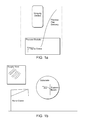
- FIG. 1 (includes FIGS. 1 a and 1 b ) shows a suitable nano construction apparatus where in FIG. 1( a ) an overview is depicted and in FIG. 1( b ) a process area with exemplary structure (beam with arc) is depicted.
- FIG. 2 shows a prefabricated nanowire which has been welded to the nanomanipulator and is being moved to the area of interest.
- FIG. 3 shows the nanowire has been placed into position and is ready for welding.
- FIG. 4 shows the nanowire has been welded in position.
- FIG. 5 shows beams crossed in air.
- An apparatus and method for constructing complex nano-scale structures or modifying existing structures has been developed. This method uses integration of technologies such as nano particle beams (for example, SEM, FIB), beam based chemistry (CVD), nano-manipulators, environmental control, and computer aided design (CAD) files to construct, analyze and modify nanoscale systems.
- technologies such as nano particle beams (for example, SEM, FIB), beam based chemistry (CVD), nano-manipulators, environmental control, and computer aided design (CAD) files to construct, analyze and modify nanoscale systems.
- this nano-construction technique is capable of building complex three dimensional structures through building construction techniques adapted to nanoscale environments.
- beams are made of nano tubes
- cranes are nano-manipulators and welders are beam based CVD or electrochemical processing.
- the raw material can be for example carbon nanotubes, beams or lines cut out of bulk metal in-situ or ex-situ that can be curved or rectangular. Gaseous precursors are used for welding pieces together under the energy of the beam, etc.
- nano-manipulator devices including e.g. nano-tweezers
- TEM sample prep device TEM sample prep device
- Zyvex Electro Mechanical Probing
- Kleindiek TEM sample prep and electrical probing
- Xidex Nanomanipulation
- a wide nanoscale system can be created in accordance with methods and systems of the invention. More specifically, particularly suitably applications for methods and systems of the invention include
- nano manipulators can position beams in such a way that they can be welded and structures built in a manner very similar to building construction. Overhanging, retrograde, high aspect ratio features are all easily built with this technique.
- a substrate is placed in a holder ( FIG. 1( a )) that incorporates at least one nano-crane and is placed inside a beam system with beam chemistry capability and CAD navigation.
- the holder is designed to be a complete construction site ready with beams of pre-cut metal, metal blocks for in-situ cutting of custom pieces, plates of insulator, a supply of carbon nanotubes (CNT's), spare nano-manipulator parts and space for custom supplies.
- CNT's carbon nanotubes
- the nano-crane may be any of a variety of nano-manipulation tools, including commercially available nano-manipulators, such as a Zyvex L100TM, which may include an x-nano-positioner and a y-nano-positioner for nano-positioning of a nano-article in the x and y directions.
- the nano-manipulator may be used for manipulation of the specimen in any of x, y or z directions.
- the length of wire needed in the construction is either immediately available or is cut to size with the system beam. It is then attached to the nano-manipulator, moved to the desired location and fused to the system under construction.
- methods of the invention were conducted in a nanofabrication facility and in a two beam (FIB/SEM) system outfitted with a nanomanipulator.
- FIB/SEM two beam
- a prefabricated nanowire is moved to the disk area.
- the wire is suitably designed to have a tab for attachment to the nanomanipulator. The tab is cut off once the wire is attached to the system.
- the wire is in position for welding and in FIG. 4 the wire has been welded using E-Beam CVD. As shown in FIG. 4 , the nanowire is welded in position.
- FIG. 5 depicts an example of a structure that would be impossible to build in planar processing where pillars are connected by crossing beams that are not touching.
- circuit editing applications are preferred aspects of the invention.
- a specific application of nanoconstruction is for the editing of integrated circuits. The ultimate verification of a circuit design is in a system after the part is manufactured.
- FIB systems are routinely used to edit circuits once first silicon is produced so that fixes and improvements can be tested out without running through the manufacturing process.
- the nano-construction technique and system are adaptable to future generations of circuit editing because not only are dimensions scaling down but also material properties are becoming increasingly critical (for example, metal re-wiring resistance).
- Table 1 is a summary of specifications that are currently state of the art and with existing techniques cannot be adequately bridged to meet the needs for many of the edits encountered already and will be even further behind in future generation of circuits.
- Custom wires e.g. metal nanowires such as copper nanowires, semiconductor nanowire such as a silicon nanowires and other such as an indinium-containing nanowire
- Resistance can be as desired and only the ends are fused/welded with impure deposition material adding minimal resistance to the edit.
- Nanowires or carbon nanotubes can be inserted directly into vias and make contact with metal interconnect or even active areas or circuit contacts.
- CNT's that are insulating on the outside and conductive on the inside are ideal for inserting in vias to connect to underlying metal.
- an insulating coating can be deposited in the via to insulate a nanowire inserted to contact underlying interconnect.
- Nanowires or CNT's can be layed out in such a fashion eliminating the issues that arise from direct write deposition techniques. Where wire might have to cross, a dielectric pad can be positioned between the crossing wires.
- a 10 micrometer diameter disk on a pedestal had its center connected to a ground terminal using a prefabricated nanobridge. The center of the disk had to be connected to the ground terminal while avoiding any disturbance of the insulating material over the rest of the disk.
- a curved beam was fabricated from silicon and was then cut from the substrate using focused ion beam (FIB) milling and then lifted with a nanomanipulator after welding the beam to the nanomanipulator using electron beam (E-Beam) chemical vapor deposition. The beam was then placed in position to ground the center of the disk and was welded to the disk and the substrate again using E-Beam chemical vapor deposition. The beam was then cut loose from the nanomanipulator using FIB milling.
- FIB focused ion beam
- E-Beam electron beam
Abstract
In one preferred aspects, methods are provided to produce a three-dimensional feature, comprising: (a) providing a nano-manipulator device; (b) positioning an article with the nano-manipulator device; and (c) manipulating the article to produce the three-dimensional feature. The invention relates to production of nanoscale systems that can be tailored with specific physical and/or electrical characteristics or need to have these characteristics modified. Methods and apparatus are presented that can construct three-dimensional nanostructures and can also modify existing nanostructures in three dimensions.
Description
This application claims the benefit of U.S. Provisional Application Ser. No. 61/171,403, filed Apr. 21, 2009, which is incorporated herein by reference in its entirety.
In one preferred aspects, methods are provided to produce a three-dimensional feature, comprising: (a) providing a nano-manipulator device; (b) positioning an article with the nano-manipulator device; and (c) manipulating the article to produce the three-dimensional feature. The invention relates to production of nanoscale systems that can be tailored with with specific physical, optical and/or electrical characteristics or need to have these characteristics modified. Methods and apparatus are presented that can construct three-dimensional nanostructures and can also modify existing nanostructures in three dimensions.
Nanoscale Systems are currently being fabricated using many techniques adopted from the semiconductor and MEMS fields. These fabrication techniques create three dimensional structures by layering materials and patterning each layer (photolithography). Although such a process can create devices in parallel and thus produce large numbers of identical devices it is limited in its vertical scale capability. The aspect ratio (AR) of most planar processes is limited to a factor of a few units in the vertical dimension over the lateral dimension (AR of 3:1, for example). As the lateral dimension shrinks, so does the vertical and is confined to no more than an aspect ratio of 5:1 or so.
Reactive Ion Etching (RIE) has been pushed to achieve large aspect ratio via milling in nanoscale systems but it is limited to certain materials and the vertical walls cannot be made perpendicular. Subsequent process steps have to conform to the shape of the RIE formed process.
The materials that lend themselves to creating these structures are also limited to a few compounds and elements (silicon and its compounds, aluminum, titanium, copper, etc). Some of these compounds or elements are also incompatible with each other and have to be processed in special ways. For example, copper will diffuse in silicon and silicon dielectrics so it has to be completely encapsulated in a different material before it can be used in electrical circuits. This limits the scalability of copper in photolithographic processes.
In the area of structure modification, a very valuable application is circuit edit. Electronic semiconductor circuits have been modified in functionality and logic by using particle beam processes. However, these processes can only generate materials that are far inferior from the manufactured material (such as copper and dielectrics). See, generally, U.S. Pat. Nos. 7,297,946 and 5,364,497.
In one aspect, the present invention mimics building construction techniques adapted to the nanoscale.
In a preferred aspect, instead of the planar process, methods and systems of the invention employ a “pick and place” system that can place prefabricated nano-wires or other nano-articles in position for construction in a manner analogous to beams that are welded together to form the frame of a building.
Apparatus useful in methods and systems of the invention may comprise a vacuum chamber where a staging area will hold the materials for construction. A nanomanipulator can act as the crane that will place the materials in position and an imaging system will provide the navigation information and energy for welding in the case of beam based direct-write CVD processing. Electrical and other feedthroughs can permit electrical fusing of nanostructures as an alternate or additional welding technique. “Bottom-up Nanoconstruction by the Welding of Individual Metallic Nanoobjects Using Nanoscale Solder”, Yong Peng, Tony Cullis and Beverley Inkson. Nano Lett., 2009, 9 (1), pp 91-96
These nanostructures (e.g. beams and wires) can be suitably fabricated and be of any of a large number of materials or compounds customized to the needs of the specific structure of interest. The pre-fabricated segments are nano-manipulated into position and beam based chemical vapor deposition processes can be used to fuse them together. A two beam system (electron and ion beams coincident on the sample) is suitably employed and exemplified herein.
Suitably, processing in methods and systems of the invention can be accomplished through a combination of beam based chemistry, special environmental conditions and electrical/electrochemical processes. A preferred approach is electron beam based chemical vapor deposition process, see “Deposition of Narrow, High Quality, Closely Spaced, but Isolated Conductors, V. V. Makarov and R. K. Jain, Proceedings of the 33rd International Symposium for Testing and Failure Analysis, Nov. 4-8, 2007, San Jose, Calif., pp 41-45. In situ sizing of raw material(s) can be easily done with one of the beams present and usually without any chemical assistance.
A specific application that will immediately benefit from such a methodology is circuit edit, the process of modifying the layout of an already fabricated integrated circuit.
In a preferred aspect, methods and systems of the invention can employ manufactured components in circuit edit thus providing identical quality of material to the manufactured component.
In a preferred aspect, methods for producing a three-dimensional feature are provided comprising: (a) providing a nano-manipulator device; (b) positioning an article with the nano-manipulator device; and (c) manipulating the article to produce the three-dimensional feature. Two or more articles may be suitably positioned with the nano-manipulator device. As discussed, in preferred aspects, semiconductor chip editing is performed with the nano-manipulator device.
As referred to herein a nano-sized feature or object will have a critical size (smallest dimension) that is less than 5,000 nm or 1000 nm, more typically less than 500 nm, even more typically 100 nm or less. For example, a wire that is 50 nm in diameter but several microns long is considered herein to be a nanowire. A layer of material that is many square microns in area but 100 nm thick is a nanolayer.
As referred to herein, “nano-manipulation” use of a “nano-manipulator device” or other similar term indicates modification, construction or creation of a three-dimensional structure, e.g. where at least two, three, four or more discrete members (e.g. nanotubes (including carbon nanotubes), nanowires) are rigidly affixed (e.g. affixing through a CVD, electrochemical process, and/thermal process). Such rigid affixing can increase volume and/or mass of each of the joined members. For instance, a first member (e.g. carbon nanotube or nanowire) upon nano-manipulation in accordance with the present invention may result in rigid affixing to one or more additional members and a volume and/or mass change of at least 5, 10, 20, 30, 40, 50, 60, 70, 80, 90, 100, 200, 300, 400, 500, 1000%. Nano-manipulation may be accomplished through incorporation of a variety of techniques (e.g. Computer Aided Design or CAD) but may include joint creation and/or volume and/or mass addition or subtraction to manipulated nano-objects.
Nano-manipulation as referred to herein may include (but is not limited to in the absence of a mass addition or subtraction) planar fabrication and processes involving moving nanoscale structures around for either imaging or to connect them to other nanostructures or to separate them from other nanostructures. For example, two nanowires grown apart can be nanomanipulated to either cross each other or make contact to electrical points in a circuit (such as pads). In another example, an electrical nano-probe is manipulated on to a metal pad or circuit line to electrically characterize it.
Other aspects of the invention are discussed infra.
An apparatus and method for constructing complex nano-scale structures or modifying existing structures has been developed. This method uses integration of technologies such as nano particle beams (for example, SEM, FIB), beam based chemistry (CVD), nano-manipulators, environmental control, and computer aided design (CAD) files to construct, analyze and modify nanoscale systems.
Unlike the existing techniques that use planar fabrication methods extended to some limited three-dimensional capability, this nano-construction technique is capable of building complex three dimensional structures through building construction techniques adapted to nanoscale environments. For example, beams are made of nano tubes, cranes are nano-manipulators and welders are beam based CVD or electrochemical processing. The raw material can be for example carbon nanotubes, beams or lines cut out of bulk metal in-situ or ex-situ that can be curved or rectangular. Gaseous precursors are used for welding pieces together under the energy of the beam, etc.
In methods and systems of the invention, a variety of commercially available nano-manipulator devices (including e.g. nano-tweezers) may be employed including e.g. devices from Omniprobe (TEM sample prep device); Zyvex (Electrical Probing); Kleindiek (TEM sample prep and electrical probing); and Xidex (Nanomanipulation).
A wide nanoscale system can be created in accordance with methods and systems of the invention. More specifically, particularly suitably applications for methods and systems of the invention include
- 1) Circuit Edit;
- 2) Construction of nano-electrical mechanical systems (NEMS), including placing gears and electrical components together to assemble a NEMS;
- 3) Photonic systems. Construction of complex nanoscale structures for optical systems (optical guides, wave guides, fiber splicers etc.);
- 4) Construction of sensors. For example, an electrical system can have a sensor to measure electrical resistivity inside a cell. This sensor has to be attached to the electrical circuit;
- 5) Medical nanodevices (these are often called NEMS, but can be different than above discussed NEMS). For example, a fluidic device that separates different particles from within a fluid or mixes fluids etc.;
- 6) Synthetic biology.
In accordance with the invention, nano manipulators can position beams in such a way that they can be welded and structures built in a manner very similar to building construction. Overhanging, retrograde, high aspect ratio features are all easily built with this technique.
Several components of this invention have already been integrated into one system but others have to be further developed and integrated. Existing nanomanipulators lack the positioning accuracy for the finest range of nanoscale accuracy and electrochemical fusing processes are an alternative to CVD welding that show a lot of promise but not yet fully developed. “Nanomanipulation by Atomic Force Microscopy, F. J. Rubio-Sierra 1, W. M. Heckl 1 2, R. W. Stark *, 1Ludwig-Maximilians-Universität München, Kristallographie and Center for Nanoscience CeNS, Theresienstr. 41, 80333 Munich, Germany, Deutsches Museum, Museumsinsel 1, 80538 Munich, Germany, Advanced Engineering Materials, Volume 7 Issue 4, Pages 193-196, Published Online: 21 Apr. 2005. Also, temperature control can have a positive effect in beam based processing; consequently, that aspect of the environmental control may become important.
Referring now to the drawings, in one preferred method, a substrate is placed in a holder (FIG. 1( a)) that incorporates at least one nano-crane and is placed inside a beam system with beam chemistry capability and CAD navigation. The holder is designed to be a complete construction site ready with beams of pre-cut metal, metal blocks for in-situ cutting of custom pieces, plates of insulator, a supply of carbon nanotubes (CNT's), spare nano-manipulator parts and space for custom supplies. The nano-crane may be any of a variety of nano-manipulation tools, including commercially available nano-manipulators, such as a Zyvex L100™, which may include an x-nano-positioner and a y-nano-positioner for nano-positioning of a nano-article in the x and y directions. The nano-manipulator may be used for manipulation of the specimen in any of x, y or z directions.
The length of wire needed in the construction is either immediately available or is cut to size with the system beam. It is then attached to the nano-manipulator, moved to the desired location and fused to the system under construction.
In one specifically preferred system, methods of the invention were conducted in a nanofabrication facility and in a two beam (FIB/SEM) system outfitted with a nanomanipulator. Using nanofabrication, wires are constructed as needed to connect the center of a disk to a pad so that the center of the disk could be grounded. The surface of the disk is covered with dielectric everywhere except the center where the doped silicon below is exposed.
As depicted in FIG. 2 , a prefabricated nanowire is moved to the disk area. The wire is suitably designed to have a tab for attachment to the nanomanipulator. The tab is cut off once the wire is attached to the system.
Next, shown in FIG. 3 , the wire is in position for welding and in FIG. 4 the wire has been welded using E-Beam CVD. As shown in FIG. 4 , the nanowire is welded in position.
The ability to connect additional structures to such a beam has been successfully carried out and with proper design structures can be built up into heights and complexities not attainable through planar processing. FIG. 5 depicts an example of a structure that would be impossible to build in planar processing where pillars are connected by crossing beams that are not touching.
As discussed above; circuit editing applications are preferred aspects of the invention. A specific application of nanoconstruction is for the editing of integrated circuits. The ultimate verification of a circuit design is in a system after the part is manufactured. Currently, FIB systems are routinely used to edit circuits once first silicon is produced so that fixes and improvements can be tested out without running through the manufacturing process. The nano-construction technique and system are adaptable to future generations of circuit editing because not only are dimensions scaling down but also material properties are becoming increasingly critical (for example, metal re-wiring resistance).
The following Table 1 is a summary of specifications that are currently state of the art and with existing techniques cannot be adequately bridged to meet the needs for many of the edits encountered already and will be even further behind in future generation of circuits.
| TABLE 1 |
| Comparison of critical specifications using extended state of the art |
| technologies and nanoconstruction |
| Figure of | Nanoconstruction | ||
| Objective | Merit | State-of-the-art | Capability |
| Metal | Line Width | 100 nm | 10 nm |
| Deposition | Line Pitch | 200 nm | 20 nm |
| Resistivity | 200 μΩcm | 2 μΩcm | |
| Dielectric | Resistivity | 109 μΩcm | 1015 μΩcm |
| Deposition | Dielectric | Unknown | ~2 |
| Constant (k) | |||
| Speed of | 10 um × 1 um × | 15 minutes | 5 minutes to |
| deposition | 1 um | place and weld | |
Custom wires (e.g. metal nanowires such as copper nanowires, semiconductor nanowire such as a silicon nanowires and other such as an indinium-containing nanowire) can be cut from bulk metal and placed where the editing needs to be routed. Resistance can be as desired and only the ends are fused/welded with impure deposition material adding minimal resistance to the edit.
Nanowires or carbon nanotubes can be inserted directly into vias and make contact with metal interconnect or even active areas or circuit contacts. CNT's that are insulating on the outside and conductive on the inside are ideal for inserting in vias to connect to underlying metal. Alternatively, an insulating coating can be deposited in the via to insulate a nanowire inserted to contact underlying interconnect.
It is often desired to run multiple edit lines of interconnect with very tight pitch (sub 100 nm). Nanowires or CNT's can be layed out in such a fashion eliminating the issues that arise from direct write deposition techniques. Where wire might have to cross, a dielectric pad can be positioned between the crossing wires.
This technique can overcome limitations with interconnect material deposition and others. Edits that are speed sensitive can be done without adjustments or limitations that current technologies impose.
The following terms and abbreviations mean the following as used herein:
- CVD—Chemical Vapor Deposition. In this context we are referring to a beam induced CVD using an organometalic precursor such as Tungsten Hexa Carbonyl
- FIB—Focused Ion Beam
- SEM—Scanning Electron Microscope
- CAD—Computer Aided Design. Electronic data file with structural information
- CNT—Carbon nanotube
- RIE—Reactive Ion Etching
All documents mentioned herein are incorporated by reference herein in their entirety. The following non-limiting Example is illustrative of the invention.
A 10 micrometer diameter disk on a pedestal had its center connected to a ground terminal using a prefabricated nanobridge. The center of the disk had to be connected to the ground terminal while avoiding any disturbance of the insulating material over the rest of the disk. A curved beam was fabricated from silicon and was then cut from the substrate using focused ion beam (FIB) milling and then lifted with a nanomanipulator after welding the beam to the nanomanipulator using electron beam (E-Beam) chemical vapor deposition. The beam was then placed in position to ground the center of the disk and was welded to the disk and the substrate again using E-Beam chemical vapor deposition. The beam was then cut loose from the nanomanipulator using FIB milling.
Claims (13)
1. A method for producing a three-dimensional structure, the method comprising:
(a) providing a nano-manipulator device;
(b) affixing a first article to the nano-manipulator device using electron-beam chemical vapor deposition;
(c) positioning the first article with the nano-manipulator device onto a second article;
(d) affixing the first article to the second article using electron-beam chemical vapor deposition, thereby producing the three-dimensional structure, wherein a mass of the first article is increased by at least 10 percent via the electron-beam chemical vapor deposition.
2. The method of claim 1 , further comprising:
(e) separating the first article from the nano-manipulator device.
3. The method of claim 2 wherein the first article is separated from the nano-manipulator device by focused ion beam milling.
4. The method of claim 1 wherein the first and second articles are selected from the group consisting of: a microelectronic device, a substrate to form a nano-electrical mechanical system, a photonic system substrate, a sensor substrate, and -a medical nanodevice.
5. The method of claim 1 or 4 wherein two or more articles are positioned with the nano-manipulator device.
6. The method of claim 1 wherein a semiconductor chip editing is performed with the nano-manipulator device.
7. The method of claim 1 wherein the mass of the first article is increased by at least 30 percent via the electron-beam chemical vapor deposition.
8. A method for producing a three-dimensional structure, the method comprising increasing mass of one or more nano-sized articles by using electron-beam chemical vapor deposition to affix one or more additional members to the one or more nano-sized articles, thereby producing the three-dimensional structure, wherein the mass of the one or more articles is increased by at least 10 percent via the electron-beam chemical vapor deposition.
9. The method of claim 8 wherein the mass of one or more articles is increased by at least 30 percent by the electron-beam chemical vapor deposition.
10. The method of claim 8 or 9 wherein the three-dimensional structure is selected from the group consisting of: a microelectronic device, a substrate to form a nano-electrical mechanical system, a photonic system substrate, a sensor substrate, and a medical nanodevice.
11. A method for producing a three-dimensional structure, comprising rigidly affixing two or more discrete nano-members using electron-beam chemical vapor deposition, wherein a mass of a particular member is increased by at least 10 percent via the electron-beam chemical vapor deposition.
12. The method of claim 11 wherein the two or more members are rigidly affixed with a nano-manipulator device.
13. The method of claim 11 or 12 wherein the two or more members are nanotubes and/or nanowires.
Priority Applications (2)
| Application Number | Priority Date | Filing Date | Title |
|---|---|---|---|
| US12/799,352 US8887381B2 (en) | 2009-04-21 | 2010-04-21 | Method of making a 3-D structure |
| US14/543,775 US20150203352A1 (en) | 2009-04-21 | 2014-11-17 | Nano-construction of complex 3-d structures and modification of existing structures |
Applications Claiming Priority (2)
| Application Number | Priority Date | Filing Date | Title |
|---|---|---|---|
| US17140309P | 2009-04-21 | 2009-04-21 | |
| US12/799,352 US8887381B2 (en) | 2009-04-21 | 2010-04-21 | Method of making a 3-D structure |
Related Child Applications (1)
| Application Number | Title | Priority Date | Filing Date |
|---|---|---|---|
| US14/543,775 Continuation US20150203352A1 (en) | 2009-04-21 | 2014-11-17 | Nano-construction of complex 3-d structures and modification of existing structures |
Publications (2)
| Publication Number | Publication Date |
|---|---|
| US20100314353A1 US20100314353A1 (en) | 2010-12-16 |
| US8887381B2 true US8887381B2 (en) | 2014-11-18 |
Family
ID=43011666
Family Applications (2)
| Application Number | Title | Priority Date | Filing Date |
|---|---|---|---|
| US12/799,352 Expired - Fee Related US8887381B2 (en) | 2009-04-21 | 2010-04-21 | Method of making a 3-D structure |
| US14/543,775 Abandoned US20150203352A1 (en) | 2009-04-21 | 2014-11-17 | Nano-construction of complex 3-d structures and modification of existing structures |
Family Applications After (1)
| Application Number | Title | Priority Date | Filing Date |
|---|---|---|---|
| US14/543,775 Abandoned US20150203352A1 (en) | 2009-04-21 | 2014-11-17 | Nano-construction of complex 3-d structures and modification of existing structures |
Country Status (2)
| Country | Link |
|---|---|
| US (2) | US8887381B2 (en) |
| WO (1) | WO2010123570A2 (en) |
Families Citing this family (2)
| Publication number | Priority date | Publication date | Assignee | Title |
|---|---|---|---|---|
| CN114279784A (en) * | 2021-12-22 | 2022-04-05 | 上海季丰电子股份有限公司 | Preparation method of transmission electron microscope sample |
| CN117464155B (en) * | 2023-12-28 | 2024-03-15 | 合肥国镜仪器科技有限公司 | Nanowire welding method and welding device |
Citations (6)
| Publication number | Priority date | Publication date | Assignee | Title |
|---|---|---|---|---|
| US5364497A (en) | 1993-08-04 | 1994-11-15 | Analog Devices, Inc. | Method for fabricating microstructures using temporary bridges |
| WO2002012443A2 (en) | 2000-08-09 | 2002-02-14 | California Institute Of Technology | Active nems arrays for biochemical analyses |
| US20050176228A1 (en) | 2003-12-11 | 2005-08-11 | Fonash Stephen J. | Controlled nanowire growth in permanent, integrated nano-templates and methods of fabricating sensor and transducer structures |
| US20070020445A1 (en) | 2005-06-01 | 2007-01-25 | The Board Of Trustees Of The University Of Illinois | Flexible Structures For Sensors And Electronics |
| US20070138705A1 (en) | 2005-08-08 | 2007-06-21 | The Reagents Of The University Of California | Shape manipulation of nanostructures |
| US7297946B2 (en) | 2004-08-16 | 2007-11-20 | Board Of Trustees Operating Michigan State University | Automated nanoassembly |
Family Cites Families (1)
| Publication number | Priority date | Publication date | Assignee | Title |
|---|---|---|---|---|
| US6265235B1 (en) * | 1999-08-25 | 2001-07-24 | Lucent Technologies, Inc. | Method of sectioning of photoresist for shape evaluation |
-
2010
- 2010-04-21 US US12/799,352 patent/US8887381B2/en not_active Expired - Fee Related
- 2010-04-21 WO PCT/US2010/001204 patent/WO2010123570A2/en active Application Filing
-
2014
- 2014-11-17 US US14/543,775 patent/US20150203352A1/en not_active Abandoned
Patent Citations (6)
| Publication number | Priority date | Publication date | Assignee | Title |
|---|---|---|---|---|
| US5364497A (en) | 1993-08-04 | 1994-11-15 | Analog Devices, Inc. | Method for fabricating microstructures using temporary bridges |
| WO2002012443A2 (en) | 2000-08-09 | 2002-02-14 | California Institute Of Technology | Active nems arrays for biochemical analyses |
| US20050176228A1 (en) | 2003-12-11 | 2005-08-11 | Fonash Stephen J. | Controlled nanowire growth in permanent, integrated nano-templates and methods of fabricating sensor and transducer structures |
| US7297946B2 (en) | 2004-08-16 | 2007-11-20 | Board Of Trustees Operating Michigan State University | Automated nanoassembly |
| US20070020445A1 (en) | 2005-06-01 | 2007-01-25 | The Board Of Trustees Of The University Of Illinois | Flexible Structures For Sensors And Electronics |
| US20070138705A1 (en) | 2005-08-08 | 2007-06-21 | The Reagents Of The University Of California | Shape manipulation of nanostructures |
Non-Patent Citations (10)
| Title |
|---|
| Characteristics of Nano-Electrostatic Actuator Fabricated by Focused Ion Beam Chemical Vapor Deposition by R. Kumetani et al, a paper in Japanese J. Appl Physics, vol. 43, No. 10, pp. 7187-7191 (2004); hereinafter Komettani et al.(1). * |
| Fabrication of Nano-Manipulator with SiO(2)DLC Hetero-Structure by Focused ion-Beam Chemical Vapor Deposition by R. Kumetani et al (2004 International. Microprocesses and Nanotechnology Conference Oct. 26-29, 2004, Japanese J. Applied Physics. * |
| International Search Report for International Application No. PCT/US2010/001204, dated Jan. 5, 2011. |
| International Search Report, International Application No. PCT/US2010/001204 (Jan. 5, 2011). |
| Makarov et al., "Deposition of Narrow, High Quality, Closely Spaced, but Isolated Conductors," Proceeding of the 33rd International Symposium for Testing and Failure Analysis, Nov. 4-8, 2007, San Jose, CA, pp. 41-45. |
| Manipulation using 3-D Nano-Manipulator Fabricated by FIB-CVD in the Nano-Factory by R. Kumetani et al (2005 International. Microprocesses and Nanotechnology Conference Oct. 25-28, 2005, paper No. publisher is Inst. of Elec. and Elec. Eng. Computer Society, paper No. 1595324. * |
| Peng et al., "Bottom-up Nanoconstruction by the Welding of Individual Metallic Nanoobjects Using Nanoscale Solder," Nano Lett., 9(1):91-96 (2009). |
| Rubio-Sierra et al., "Nanomanipulation by Atomic Force Microscopy," Advanced Engineering Materials, 7(4):193-196 (2005). |
| Written Opinion for International Application No. PCT/US2010/001204, dated Jan. 5, 2011. |
| Written Opinion of the International Searching Authority, International Application PCT/US2010/001204 (Jan. 5, 2011). |
Also Published As
| Publication number | Publication date |
|---|---|
| WO2010123570A2 (en) | 2010-10-28 |
| US20100314353A1 (en) | 2010-12-16 |
| US20150203352A1 (en) | 2015-07-23 |
| WO2010123570A3 (en) | 2011-03-10 |
Similar Documents
| Publication | Publication Date | Title |
|---|---|---|
| Ru et al. | Automated four-point probe measurement of nanowires inside a scanning electron microscope | |
| JP6247289B2 (en) | Three-dimensional crystalline, homogeneous and composite nanostructures prepared by field-induced assembly of nanoelements | |
| Joachim et al. | Multiple atomic scale solid surface interconnects for atom circuits and molecule logic gates | |
| US20050285275A1 (en) | Fabrication of nano-gap electrode arrays by the construction and selective chemical etching of nano-crosswire stacks | |
| JP2010532717A (en) | Nanotube device and manufacturing method | |
| US8692385B2 (en) | Device for connecting nano-objects to external electrical systems, and method for producing said device | |
| Jeon et al. | Fabrication of complex three-dimensional nanostructures using focused ion beam and nanomanipulation | |
| US8887381B2 (en) | Method of making a 3-D structure | |
| Heeres et al. | A compact multipurpose nanomanipulator for use inside a scanning electron microscope | |
| Xu et al. | Recent developments in focused ion beam and its application in nanotechnology | |
| Cole et al. | Mimicking Electrodeposition in the Gas Phase: A Programmable Concept for Selected‐Area Fabrication of Multimaterial Nanostructures | |
| Haas et al. | Aligned Stacking of Nanopatterned 2D Materials for High-Resolution 3D Device Fabrication | |
| Orlov et al. | Shape memory effect nanotools for nano-creation: examples of nanowire-based devices with charge density waves | |
| Qu et al. | Investigating the impact of SEM chamber conditions and imaging parameters on contact resistance of in situ nanoprobing | |
| JP4991206B2 (en) | Micromanipulation device for microscopic work | |
| JP2005111583A (en) | Method of manufacturing structure of nanometer scale | |
| US8819926B2 (en) | Methods and apparatuses of using metal needle arrays for specimen lift-out and circuit edit | |
| US20080067440A1 (en) | Machining of microstructures | |
| Li et al. | Three-dimensional nanostructures by focused ion beam techniques: Fabrication and characterization | |
| Wang et al. | Development of a thermoelectric nanowire characterization platform (TNCP) for structural and thermoelectric investigation of single nanowires | |
| US20140338076A1 (en) | Methods and Apparatuses for Specimen Lift-Out and Circuit Edit Using Needle Arrays | |
| Raffa et al. | Focused ion beam as a scanning probe: Methods and applications | |
| TWI450854B (en) | 3d nanochannel device and method of manufacturing the same | |
| Nellen et al. | Preparative methods for nanoanalysis of materials with focused ion beam instruments | |
| Sapkov et al. | Method of creation of monomolecular transistor with overhanging electrodes |
Legal Events
| Date | Code | Title | Description |
|---|---|---|---|
| FEPP | Fee payment procedure |
Free format text: MAINTENANCE FEE REMINDER MAILED (ORIGINAL EVENT CODE: REM.) |
|
| LAPS | Lapse for failure to pay maintenance fees |
Free format text: PATENT EXPIRED FOR FAILURE TO PAY MAINTENANCE FEES (ORIGINAL EVENT CODE: EXP.); ENTITY STATUS OF PATENT OWNER: SMALL ENTITY |
|
| STCH | Information on status: patent discontinuation |
Free format text: PATENT EXPIRED DUE TO NONPAYMENT OF MAINTENANCE FEES UNDER 37 CFR 1.362 |
|
| FP | Lapsed due to failure to pay maintenance fee |
Effective date: 20181118 |