US8890338B2 - Method of identifying and/or programming an integrated circuit - Google Patents
Method of identifying and/or programming an integrated circuit Download PDFInfo
- Publication number
- US8890338B2 US8890338B2 US11/535,866 US53586606A US8890338B2 US 8890338 B2 US8890338 B2 US 8890338B2 US 53586606 A US53586606 A US 53586606A US 8890338 B2 US8890338 B2 US 8890338B2
- Authority
- US
- United States
- Prior art keywords
- integrated circuit
- programming
- pads
- programming pads
- chip
- Prior art date
- Legal status (The legal status is an assumption and is not a legal conclusion. Google has not performed a legal analysis and makes no representation as to the accuracy of the status listed.)
- Expired - Fee Related, expires
Links
Images


Classifications
-
- H—ELECTRICITY
- H01—ELECTRIC ELEMENTS
- H01L—SEMICONDUCTOR DEVICES NOT COVERED BY CLASS H10
- H01L23/00—Details of semiconductor or other solid state devices
- H01L23/52—Arrangements for conducting electric current within the device in operation from one component to another, i.e. interconnections, e.g. wires, lead frames
- H01L23/522—Arrangements for conducting electric current within the device in operation from one component to another, i.e. interconnections, e.g. wires, lead frames including external interconnections consisting of a multilayer structure of conductive and insulating layers inseparably formed on the semiconductor body
- H01L23/525—Arrangements for conducting electric current within the device in operation from one component to another, i.e. interconnections, e.g. wires, lead frames including external interconnections consisting of a multilayer structure of conductive and insulating layers inseparably formed on the semiconductor body with adaptable interconnections
-
- H—ELECTRICITY
- H01—ELECTRIC ELEMENTS
- H01L—SEMICONDUCTOR DEVICES NOT COVERED BY CLASS H10
- H01L23/00—Details of semiconductor or other solid state devices
- H01L23/48—Arrangements for conducting electric current to or from the solid state body in operation, e.g. leads, terminal arrangements ; Selection of materials therefor
-
- H—ELECTRICITY
- H01—ELECTRIC ELEMENTS
- H01L—SEMICONDUCTOR DEVICES NOT COVERED BY CLASS H10
- H01L23/00—Details of semiconductor or other solid state devices
- H01L23/544—Marks applied to semiconductor devices or parts, e.g. registration marks, alignment structures, wafer maps
-
- H—ELECTRICITY
- H01—ELECTRIC ELEMENTS
- H01L—SEMICONDUCTOR DEVICES NOT COVERED BY CLASS H10
- H01L24/00—Arrangements for connecting or disconnecting semiconductor or solid-state bodies; Methods or apparatus related thereto
- H01L24/01—Means for bonding being attached to, or being formed on, the surface to be connected, e.g. chip-to-package, die-attach, "first-level" interconnects; Manufacturing methods related thereto
- H01L24/10—Bump connectors ; Manufacturing methods related thereto
- H01L24/11—Manufacturing methods
-
- H—ELECTRICITY
- H01—ELECTRIC ELEMENTS
- H01L—SEMICONDUCTOR DEVICES NOT COVERED BY CLASS H10
- H01L2223/00—Details relating to semiconductor or other solid state devices covered by the group H01L23/00
- H01L2223/544—Marks applied to semiconductor devices or parts
- H01L2223/54433—Marks applied to semiconductor devices or parts containing identification or tracking information
- H01L2223/5444—Marks applied to semiconductor devices or parts containing identification or tracking information for electrical read out
-
- H—ELECTRICITY
- H01—ELECTRIC ELEMENTS
- H01L—SEMICONDUCTOR DEVICES NOT COVERED BY CLASS H10
- H01L2924/00—Indexing scheme for arrangements or methods for connecting or disconnecting semiconductor or solid-state bodies as covered by H01L24/00
- H01L2924/10—Details of semiconductor or other solid state devices to be connected
- H01L2924/11—Device type
- H01L2924/14—Integrated circuits
Definitions
- This invention relates to semiconductor integrated circuits and, more particularly, to methods and designs for identification and personalization of semiconductor integrated circuits.
- wafer-level test In the manufacture of semiconductor integrated circuits, semiconductor chips are functionally tested at the wafer-level and then again after the chips are packaged. These tests are generally referred to as “wafer-level test” and “final test,” respectively.
- the wafer-level test confirms circuit functionality and final test confirms that the packaged chip works as intended.
- Integrated circuit identification information may include process lot number, wafer number and position on the wafer, and/or a chip serial number. This information can be used to determine causes of integrated circuit failures which occur during normal testing, such as during final test, as well as during field operation. Without chip identification information it is often difficult to relate a failure to specific integrated circuit parameters.
- redundant circuitry In the manufacture of memory chips, redundant circuitry is often built into memory arrays to achieve full functionality when the array has a limited number of defective rows or columns. However, redundant circuitry increases the complexity of a integrated circuit and consumes costly die area.
- An alternative approach to the memory yield problem uses a large memory array divided into a plurality of sub-memory regions or blocks, and only the fully functional sub-memory regions are identified for use.
- a chip identification circuit is coupled to an on-chip memory control unit to provide information on the functional memory size. For the redundant memory approach, a chip identification circuit disables the defective row and/or column and substitutes a redundant row and/or column. See, for example, Cenker et al., U.S. Pat. No. 4,228,528. Both approaches rely on a form of chip identification for proper operation of the memory chip.
- chip identification involves “trimming” (i.e., electrically adjusting or modifying) individual chips after wafer processing is complete in order to, for example, provide compensation to analog circuits for manufacturing variation. It may also be used to provide chip “personalization,” where certain functions of the chip are enabled or disabled after manufacture.
- OTP one-time programmable read only memory
- ROM read only memory
- Programming mechanisms for OTP memory circuits include use of laser-blown fuses, electrically blown fuses and anti-fuses, and floating-gate technology.
- floating-gate and anti-fuse ROM circuits may require additional wafer processing steps to form the structures to be programmed.
- all of the techniques require additional circuitry that consumes costly silicon die area.
- laser fusing requires precision alignment of the laser and the laser's energy must be tightly controlled to avoid damaging the chip being programmed.
- One disclosed embodiment of the invention provides a fabrication method of manufacturing integrated circuit having a substrate.
- a plurality of active devices are formed on the substrate and multiple metallization levels are formed over the active devices to interconnect some of the active devices, thereby forming programmable circuitry.
- the multiple metal layers have a bond pad level on which programming pads are formed.
- the programming pads are wired to the programmable circuitry. Two or more of programming pads may be selectively coupled together to program the programmable circuitry.
- Another disclosed embodiment of the invention is an integrated circuit having a semiconductor substrate, a plurality of active devices on the substrate, multiple metallization levels over the active devices, and programming pads.
- the multiple metallization levels have a bond-pad level and the programming pads are formed on the bond-pad level. Two or more of the programming pads are adapted to be selectively coupled to one another.
- FIG. 1 schematically illustrates a chip identification circuit
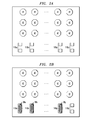
- FIGS. 2A-2D are partial plan views of programming pads and solder ball pads after various stages of fabrication.
- FIGS. 3A-3D are partial cross-sectional views of the structure of FIGS. 2A-2D after various stages of fabrication;
- a chip identification circuit 10 embodied in an integrated circuit or chip (not shown) and according to an embodiment of the present invention, comprises programming circuitry 11 and shift register circuitry 12 .
- the programming circuitry 11 includes an exemplary sequence of pairs of spaced-apart programming pads 110 a - 110 z adapted for selective connection or “programming.”
- the sequence of pads 110 a - 110 z is selectively programmed by the addition of a conductive link 111 a - 111 y . In this example, pad pair 110 z is not so programmed.
- a logic-low state is indicated, while for the pads in each pair that are shorted together with the conductive link 111 a - 111 y , a logic-high state is indicated.
- the logic levels “high” and “low” are arbitrary and merely illustrate the functionality of the circuitry 11 .
- the pairs of pads 110 a - 110 z may conduct analog signals or logic signals of any level between logic gates or other circuitry and are not limited to simple static logic applications. It is also understood that other configurations of the pads may be used.
- Shift register circuitry 12 takes the logic values from the circuitry 11 for further application with in the integrated circuit.
- Each AND gate 130 a - 130 z has a corresponding first input terminal 131 a - 131 z , a corresponding second input terminal 132 a - 132 z and a corresponding output terminal 133 a - 133 z .
- the first input terminal 131 a - 131 z of each AND gate 130 a - 130 z is connected to one pad in the corresponding pair of pads 110 a - 110 z . If a pair of pads is programmed to a logic-high state, the first AND gate input receives a voltage level based on a connection to V DD .
- the second input 132 a - 132 z to each AND gate 130 a - 130 z is responsive to a LOAD signal.
- the LOAD is a logic-high voltage signal applied to second input 132 a - 132 z , when the programmed sequence of pads 110 a - 110 z are to be read.
- the output terminal 133 a - 133 z of each AND gate indicates the programmed status (logic-high or logic-low) of the pair of pads to which it is connected when the LOAD signal is asserted.
- the shift register circuitry 12 also includes a plurality of flip-flops 140 a - 140 z , connected to each other in series. Each flip-flop 140 a - 140 z receives a logic-high or logic-low signal from a corresponding AND gate output terminal 133 a - 133 z . To read the programming circuitry, the shift register circuitry is reset or cleared in response to a logic-high clear signal CLR. Then the data programmed into the pairs of pads 110 a - 110 z is loaded into the flip-flops 140 a - 140 z when the LOAD signals goes logical high, enabling the AND gates 130 a - 130 z so that the logic value on each AND gate output terminal is stored in an associated flip-flop.
- the shift register circuitry 12 then generates a serial output signal corresponding to the logic levels stored in the flip-flops and in accord with a clock signal CLK which controls serial movement of values stored in the flip-flops from one flip-flop to a next flip flop and ultimately to the shift register output terminal 141 .
- the programming of chip identification information can made in the programming circuitry 11 after wafer level testing is complete.
- Maskless deposition of conductive material for example, by ink-jet discharge of a conductive ink comprising materials such as metallic particles, conductive polymer, or carbon particles
- TFT thin film transistor
- LCD liquid crystal display
- a non-conducting, protective coating material for example, ink-jet discharge of non-conducting epoxy.
- the functional dies are cut for individual packaging and solder balls are formed thereon for ball grid array packages.
- die singulation can be performed prior to maskless deposition of conductive material over the programming pads.
- FIGS. 2A-2D sequentially illustrate, in partial plan views, programming pads and solder ball landing pads during a sequence of fabrication and programming steps.
- a series of programming pad pairs 110 a - 110 z are shown along with an array of solder ball landing pads 41 , for receiving solder balls 42 , formed on an upper level of metallization in an interconnect system.
- selected pairs of programming pads 110 a - 110 y are connected by maskless selective deposition of conductive film 38 a - 38 y as shown in FIG. 2B to provide a conductive link between pairs of pads 110 a - 110 y , while pad pair 110 z is not connected.
- FIG. 2A a series of programming pad pairs 110 a - 110 z are shown along with an array of solder ball landing pads 41 , for receiving solder balls 42 , formed on an upper level of metallization in an interconnect system.
- selected pairs of programming pads 110 a - 110 y are connected by maskless selective deposition of conductive film 38 a - 38
- a non-conductive protective material 39 is shown deposited by a maskless deposition method over the entire programming pad area after the pairs 110 a - 110 z are programmed.
- solder balls 42 are then placed on the solder ball landing pads 41 .
- FIGS. 3A-3D are partial cross-sectional views, taken along by line A-A′ of FIG. 2C , illustrating a portion of the programming circuitry 11 formed on a semiconductor substrate 30 of an integrated circuit 20 with maskless deposition of conductive material.
- individual metal contact pads 35 a and 35 b are shown formed on an upper level 15 L (also referred to as a bond-pad level) of a multi-level interconnect structure.
- Each pad 35 a , 35 b is shown connected through a first passivation layer 36 to one of the pads 37 a , 37 b in the pair 110 a of programming pads.
- one metal pad 35 a is connected to the supply voltage V DD terminal through underlying metal vias 34 a and metal runner segments 32 a .
- the other metal pad 35 b is connected to the AND gate 130 a shown in FIG. 1 through underlying metal vias 34 b and metal runner segments 32 b .
- the conductive material 38 a is deposited over and between the programming pads 37 a and 37 b by the maskless selective deposition method as discussed above
- a non-conductive protective coating material 39 preferably a polymer such as epoxy, is deposited over the conductive material 38 a and part of second passivation layer 40 , preferably also by an ink-jet discharge method, to protect the programming pads from the environment.
- the second dielectric material 40 of the dual passivation structure used in solder ball packages may cover the programming pads.
- FIGS. 2A-2D , 3 A- 3 C may be utilized for testing the chip 20 at the wafer level or for final test after packaging the chip in a ceramic package or the like where the chip 20 remains exposed (a lid to the package is mounted after final test to completely seal the packaged chip).
- the chip is completely encapsulated, making programming at final test essentially impossible.
- FIG. 3D shows an alternative embodiment of the invention. While similar to that shown in FIG. 3C , a conventional plastic encapsulation layer 50 is added prior to the deposition of conductive material 38 a and protective layer 39 but leaving the pads 37 a , 37 b and surrounding area expose.
- the chip 20 can be programmed at a convenient time and for purposes other than redundancy programming, such as programming a serial number into the chip.
- the protective layer 39 also completes encapsulation of the chip against environmental contamination.
- the present invention may also be applied to the wire bond packages prior to encapsulation of the integrated circuit
- the individual die are cut and sorted for packaging. Wire bonding is then performed followed by encapsulation of each die.
Abstract
Description
Claims (8)
Priority Applications (5)
| Application Number | Priority Date | Filing Date | Title |
|---|---|---|---|
| US11/535,866 US8890338B2 (en) | 2006-09-27 | 2006-09-27 | Method of identifying and/or programming an integrated circuit |
| KR1020070096329A KR101460355B1 (en) | 2006-09-27 | 2007-09-21 | Method of identifying and/or programming an integrated circuit |
| JP2007250732A JP2008085342A (en) | 2006-09-27 | 2007-09-27 | Method for identifying and/or programming integrated circuit |
| CNA2007101616059A CN101154626A (en) | 2006-09-27 | 2007-09-27 | Method of identifying and/or programming an integrated circuit |
| TW096135963A TW200828481A (en) | 2006-09-27 | 2007-09-27 | Method of identifying and/or programming an integrated circuit |
Applications Claiming Priority (1)
| Application Number | Priority Date | Filing Date | Title |
|---|---|---|---|
| US11/535,866 US8890338B2 (en) | 2006-09-27 | 2006-09-27 | Method of identifying and/or programming an integrated circuit |
Publications (2)
| Publication Number | Publication Date |
|---|---|
| US20080073789A1 US20080073789A1 (en) | 2008-03-27 |
| US8890338B2 true US8890338B2 (en) | 2014-11-18 |
Family
ID=39224069
Family Applications (1)
| Application Number | Title | Priority Date | Filing Date |
|---|---|---|---|
| US11/535,866 Expired - Fee Related US8890338B2 (en) | 2006-09-27 | 2006-09-27 | Method of identifying and/or programming an integrated circuit |
Country Status (5)
| Country | Link |
|---|---|
| US (1) | US8890338B2 (en) |
| JP (1) | JP2008085342A (en) |
| KR (1) | KR101460355B1 (en) |
| CN (1) | CN101154626A (en) |
| TW (1) | TW200828481A (en) |
Cited By (4)
| Publication number | Priority date | Publication date | Assignee | Title |
|---|---|---|---|---|
| US10269635B2 (en) | 2016-02-19 | 2019-04-23 | Infineon Technologies Ag | Integrated circuit substrate and method for manufacturing the same |
| US10340197B2 (en) | 2016-02-19 | 2019-07-02 | Infineon Technologies Ag | Integrated circuit substrate having configurable circuit elements |
| US10580753B2 (en) | 2017-07-21 | 2020-03-03 | Infineon Technologies Ag | Method for manufacturing semiconductor devices |
| US20220246566A1 (en) * | 2021-01-29 | 2022-08-04 | Texas Instruments Incorporated | Multi-function bond pad |
Families Citing this family (8)
| Publication number | Priority date | Publication date | Assignee | Title |
|---|---|---|---|---|
| DE102007003514B3 (en) * | 2007-01-19 | 2008-05-29 | Atmel Germany Gmbh | Falsification safety providing method for product e.g. garment, involves assigning marking to identifier in set or deleted condition, and permitting read access on identifier by reader after authentication during set condition of marking |
| US8088634B2 (en) | 2008-11-11 | 2012-01-03 | Johnson Morgan T | Methods of adding pads and one or more interconnect layers to the passivated topside of a wafer including connections to at least a portion of the integrated circuit pads thereon |
| KR101083640B1 (en) * | 2009-07-31 | 2011-11-16 | 주식회사 하이닉스반도체 | Fuse part in semiconductor device and method for fabricating the same |
| JP2016009840A (en) * | 2014-06-26 | 2016-01-18 | 富士通セミコンダクター株式会社 | Semiconductor device, repairing method of semiconductor device, and method of manufacturing semiconductor device |
| GB2546761B (en) * | 2016-01-27 | 2020-07-22 | Neudrive Ltd | Methods and circuits |
| DE102017103310A1 (en) * | 2016-02-19 | 2017-08-24 | Infineon Technologies Ag | SUBSTRATE OF AN ELECTRONIC DEVICE AND METHOD FOR MANUFACTURING THEREOF |
| CN106057823B (en) * | 2016-07-29 | 2019-05-10 | 京东方科技集团股份有限公司 | A kind of array substrate and preparation method thereof, display device |
| US11004484B2 (en) | 2018-06-15 | 2021-05-11 | Samsung Electronics Co., Ltd. | Page buffer and memory device including the same |
Citations (8)
| Publication number | Priority date | Publication date | Assignee | Title |
|---|---|---|---|---|
| JPS5764941A (en) | 1980-10-09 | 1982-04-20 | Hitachi Ltd | Semiconductor integrated circuit device |
| JPH0536683A (en) | 1991-08-01 | 1993-02-12 | Hitachi Ltd | Manufacture of wiring device |
| US5281684A (en) * | 1992-04-30 | 1994-01-25 | Motorola, Inc. | Solder bumping of integrated circuit die |
| JP2001135794A (en) | 1999-11-04 | 2001-05-18 | Rohm Co Ltd | Semiconductor device and trimming method for the same |
| US20030030153A1 (en) * | 2001-08-10 | 2003-02-13 | Guy Perry | Bond pad structure comprising multiple bond pads with metal overlap |
| US6864587B2 (en) | 2002-10-08 | 2005-03-08 | Renesas Technology Corp. | Semiconductor device |
| JP2005353728A (en) | 2004-06-09 | 2005-12-22 | Mitsubishi Electric Corp | High-frequency device |
| US20080003718A1 (en) * | 2006-06-30 | 2008-01-03 | Erwin Remoblas Estepa | Singulation Process for Block-Molded Packages |
-
2006
- 2006-09-27 US US11/535,866 patent/US8890338B2/en not_active Expired - Fee Related
-
2007
- 2007-09-21 KR KR1020070096329A patent/KR101460355B1/en not_active IP Right Cessation
- 2007-09-27 CN CNA2007101616059A patent/CN101154626A/en active Pending
- 2007-09-27 JP JP2007250732A patent/JP2008085342A/en active Pending
- 2007-09-27 TW TW096135963A patent/TW200828481A/en unknown
Patent Citations (8)
| Publication number | Priority date | Publication date | Assignee | Title |
|---|---|---|---|---|
| JPS5764941A (en) | 1980-10-09 | 1982-04-20 | Hitachi Ltd | Semiconductor integrated circuit device |
| JPH0536683A (en) | 1991-08-01 | 1993-02-12 | Hitachi Ltd | Manufacture of wiring device |
| US5281684A (en) * | 1992-04-30 | 1994-01-25 | Motorola, Inc. | Solder bumping of integrated circuit die |
| JP2001135794A (en) | 1999-11-04 | 2001-05-18 | Rohm Co Ltd | Semiconductor device and trimming method for the same |
| US20030030153A1 (en) * | 2001-08-10 | 2003-02-13 | Guy Perry | Bond pad structure comprising multiple bond pads with metal overlap |
| US6864587B2 (en) | 2002-10-08 | 2005-03-08 | Renesas Technology Corp. | Semiconductor device |
| JP2005353728A (en) | 2004-06-09 | 2005-12-22 | Mitsubishi Electric Corp | High-frequency device |
| US20080003718A1 (en) * | 2006-06-30 | 2008-01-03 | Erwin Remoblas Estepa | Singulation Process for Block-Molded Packages |
Cited By (5)
| Publication number | Priority date | Publication date | Assignee | Title |
|---|---|---|---|---|
| US10269635B2 (en) | 2016-02-19 | 2019-04-23 | Infineon Technologies Ag | Integrated circuit substrate and method for manufacturing the same |
| US10340197B2 (en) | 2016-02-19 | 2019-07-02 | Infineon Technologies Ag | Integrated circuit substrate having configurable circuit elements |
| US10580753B2 (en) | 2017-07-21 | 2020-03-03 | Infineon Technologies Ag | Method for manufacturing semiconductor devices |
| US20220246566A1 (en) * | 2021-01-29 | 2022-08-04 | Texas Instruments Incorporated | Multi-function bond pad |
| US11574884B2 (en) * | 2021-01-29 | 2023-02-07 | Texas Instruments Incorporated | Multi-function bond pad |
Also Published As
| Publication number | Publication date |
|---|---|
| CN101154626A (en) | 2008-04-02 |
| KR101460355B1 (en) | 2014-11-10 |
| JP2008085342A (en) | 2008-04-10 |
| US20080073789A1 (en) | 2008-03-27 |
| KR20080028794A (en) | 2008-04-01 |
| TW200828481A (en) | 2008-07-01 |
Similar Documents
| Publication | Publication Date | Title |
|---|---|---|
| US8890338B2 (en) | Method of identifying and/or programming an integrated circuit | |
| KR100893310B1 (en) | Semiconductor device and manufacturing method of same | |
| US6831294B1 (en) | Semiconductor integrated circuit device having bump electrodes for signal or power only, and testing pads that are not coupled to bump electrodes | |
| US5506499A (en) | Multiple probing of an auxilary test pad which allows for reliable bonding to a primary bonding pad | |
| KR100399493B1 (en) | Mixed fuse technologies | |
| US6861742B2 (en) | Wafer level chip size package having rerouting layers | |
| US6366209B2 (en) | Method and apparatus for early detection of reliability degradation of electronic devices | |
| US5294812A (en) | Semiconductor device having identification region for carrying out failure analysis | |
| US20060121650A1 (en) | Method and apparatus for circuit completion through the use of ball bonds or other connections during the formation of a semiconductor device | |
| TW201324519A (en) | Memory die self-disable if programmable element is not trusted | |
| US20100155885A1 (en) | Fuse Corner Pad for an Integrated Circuit | |
| EP2195843B1 (en) | Programmable rom using two bonded strata and method of operation | |
| JPH11176901A (en) | Manufacture of emulation circuit device and device having two integrated circuits | |
| JP2009021398A (en) | Semiconductor chip and method of writing process device information to semiconductor chip | |
| CN117727693A (en) | Semiconductor chip and method of producing semiconductor package including the same | |
| JPS63202938A (en) | Master slice type semiconductor device |
Legal Events
| Date | Code | Title | Description |
|---|---|---|---|
| AS | Assignment |
Owner name: AGERE SYSTEMS, INC., PENNSYLVANIA Free format text: ASSIGNMENT OF ASSIGNORS INTEREST;ASSIGNOR:HARRIS, EDWARD B.;REEL/FRAME:018315/0162 Effective date: 20060920 |
|
| AS | Assignment |
Owner name: DEUTSCHE BANK AG NEW YORK BRANCH, AS COLLATERAL AG Free format text: PATENT SECURITY AGREEMENT;ASSIGNORS:LSI CORPORATION;AGERE SYSTEMS LLC;REEL/FRAME:032856/0031 Effective date: 20140506 |
|
| AS | Assignment |
Owner name: AVAGO TECHNOLOGIES GENERAL IP (SINGAPORE) PTE. LTD Free format text: ASSIGNMENT OF ASSIGNORS INTEREST;ASSIGNOR:AGERE SYSTEMS LLC;REEL/FRAME:035365/0634 Effective date: 20140804 |
|
| AS | Assignment |
Owner name: LSI CORPORATION, CALIFORNIA Free format text: TERMINATION AND RELEASE OF SECURITY INTEREST IN PATENT RIGHTS (RELEASES RF 032856-0031);ASSIGNOR:DEUTSCHE BANK AG NEW YORK BRANCH, AS COLLATERAL AGENT;REEL/FRAME:037684/0039 Effective date: 20160201 Owner name: AGERE SYSTEMS LLC, PENNSYLVANIA Free format text: TERMINATION AND RELEASE OF SECURITY INTEREST IN PATENT RIGHTS (RELEASES RF 032856-0031);ASSIGNOR:DEUTSCHE BANK AG NEW YORK BRANCH, AS COLLATERAL AGENT;REEL/FRAME:037684/0039 Effective date: 20160201 |
|
| AS | Assignment |
Owner name: BANK OF AMERICA, N.A., AS COLLATERAL AGENT, NORTH CAROLINA Free format text: PATENT SECURITY AGREEMENT;ASSIGNOR:AVAGO TECHNOLOGIES GENERAL IP (SINGAPORE) PTE. LTD.;REEL/FRAME:037808/0001 Effective date: 20160201 Owner name: BANK OF AMERICA, N.A., AS COLLATERAL AGENT, NORTH Free format text: PATENT SECURITY AGREEMENT;ASSIGNOR:AVAGO TECHNOLOGIES GENERAL IP (SINGAPORE) PTE. LTD.;REEL/FRAME:037808/0001 Effective date: 20160201 |
|
| AS | Assignment |
Owner name: AVAGO TECHNOLOGIES GENERAL IP (SINGAPORE) PTE. LTD., SINGAPORE Free format text: TERMINATION AND RELEASE OF SECURITY INTEREST IN PATENTS;ASSIGNOR:BANK OF AMERICA, N.A., AS COLLATERAL AGENT;REEL/FRAME:041710/0001 Effective date: 20170119 Owner name: AVAGO TECHNOLOGIES GENERAL IP (SINGAPORE) PTE. LTD Free format text: TERMINATION AND RELEASE OF SECURITY INTEREST IN PATENTS;ASSIGNOR:BANK OF AMERICA, N.A., AS COLLATERAL AGENT;REEL/FRAME:041710/0001 Effective date: 20170119 |
|
| FEPP | Fee payment procedure |
Free format text: MAINTENANCE FEE REMINDER MAILED (ORIGINAL EVENT CODE: REM.) |
|
| LAPS | Lapse for failure to pay maintenance fees |
Free format text: PATENT EXPIRED FOR FAILURE TO PAY MAINTENANCE FEES (ORIGINAL EVENT CODE: EXP.); ENTITY STATUS OF PATENT OWNER: LARGE ENTITY |
|
| STCH | Information on status: patent discontinuation |
Free format text: PATENT EXPIRED DUE TO NONPAYMENT OF MAINTENANCE FEES UNDER 37 CFR 1.362 |
|
| FP | Lapsed due to failure to pay maintenance fee |
Effective date: 20181118 |