US8908383B1 - Thermal via structures with surface features - Google Patents
Thermal via structures with surface features Download PDFInfo
- Publication number
- US8908383B1 US8908383B1 US13/476,923 US201213476923A US8908383B1 US 8908383 B1 US8908383 B1 US 8908383B1 US 201213476923 A US201213476923 A US 201213476923A US 8908383 B1 US8908383 B1 US 8908383B1
- Authority
- US
- United States
- Prior art keywords
- substrate
- thermal via
- dimensions
- via structure
- electronic component
- Prior art date
- Legal status (The legal status is an assumption and is not a legal conclusion. Google has not performed a legal analysis and makes no representation as to the accuracy of the status listed.)
- Active, expires
Links
Images


Classifications
-
- H—ELECTRICITY
- H05—ELECTRIC TECHNIQUES NOT OTHERWISE PROVIDED FOR
- H05K—PRINTED CIRCUITS; CASINGS OR CONSTRUCTIONAL DETAILS OF ELECTRIC APPARATUS; MANUFACTURE OF ASSEMBLAGES OF ELECTRICAL COMPONENTS
- H05K1/00—Printed circuits
- H05K1/02—Details
- H05K1/0201—Thermal arrangements, e.g. for cooling, heating or preventing overheating
- H05K1/0203—Cooling of mounted components
- H05K1/0204—Cooling of mounted components using means for thermal conduction connection in the thickness direction of the substrate
- H05K1/0206—Cooling of mounted components using means for thermal conduction connection in the thickness direction of the substrate by printed thermal vias
-
- H—ELECTRICITY
- H05—ELECTRIC TECHNIQUES NOT OTHERWISE PROVIDED FOR
- H05K—PRINTED CIRCUITS; CASINGS OR CONSTRUCTIONAL DETAILS OF ELECTRIC APPARATUS; MANUFACTURE OF ASSEMBLAGES OF ELECTRICAL COMPONENTS
- H05K2201/00—Indexing scheme relating to printed circuits covered by H05K1/00
- H05K2201/09—Shape and layout
- H05K2201/09209—Shape and layout details of conductors
- H05K2201/095—Conductive through-holes or vias
- H05K2201/09563—Metal filled via
-
- H—ELECTRICITY
- H05—ELECTRIC TECHNIQUES NOT OTHERWISE PROVIDED FOR
- H05K—PRINTED CIRCUITS; CASINGS OR CONSTRUCTIONAL DETAILS OF ELECTRIC APPARATUS; MANUFACTURE OF ASSEMBLAGES OF ELECTRICAL COMPONENTS
- H05K2201/00—Indexing scheme relating to printed circuits covered by H05K1/00
- H05K2201/09—Shape and layout
- H05K2201/09209—Shape and layout details of conductors
- H05K2201/095—Conductive through-holes or vias
- H05K2201/0959—Plated through-holes or plated blind vias filled with insulating material
-
- H—ELECTRICITY
- H05—ELECTRIC TECHNIQUES NOT OTHERWISE PROVIDED FOR
- H05K—PRINTED CIRCUITS; CASINGS OR CONSTRUCTIONAL DETAILS OF ELECTRIC APPARATUS; MANUFACTURE OF ASSEMBLAGES OF ELECTRICAL COMPONENTS
- H05K2201/00—Indexing scheme relating to printed circuits covered by H05K1/00
- H05K2201/09—Shape and layout
- H05K2201/09818—Shape or layout details not covered by a single group of H05K2201/09009 - H05K2201/09809
- H05K2201/09854—Hole or via having special cross-section, e.g. elliptical
-
- H—ELECTRICITY
- H05—ELECTRIC TECHNIQUES NOT OTHERWISE PROVIDED FOR
- H05K—PRINTED CIRCUITS; CASINGS OR CONSTRUCTIONAL DETAILS OF ELECTRIC APPARATUS; MANUFACTURE OF ASSEMBLAGES OF ELECTRICAL COMPONENTS
- H05K2201/00—Indexing scheme relating to printed circuits covered by H05K1/00
- H05K2201/10—Details of components or other objects attached to or integrated in a printed circuit board
- H05K2201/10007—Types of components
- H05K2201/10098—Components for radio transmission, e.g. radio frequency identification [RFID] tag, printed or non-printed antennas
Definitions
- Embodiments of the present disclosure generally relate to the field of integrated circuits, and more particularly, to a substrate having thermal via structures with surface features.
- High power microelectronic packages dissipate large densities of thermal energy.
- An array of thermal vias may be used to provide a thermal channel through a substrate to direct thermal energy away from an operating electronic device.
- Via-bar structures similar to thermal vias yet having a greater heat-conducting cross-sectional area, have been increasingly used to reduce thermal resistances in the thermal channel as compared to thermal vias.
- conventional via-bar structures may be associated with package stress and, therefore, reduced device reliability.
- FIG. 1 illustrates a cross-section view of an integrated circuit (IC) device according to various embodiments.
- FIG. 2 illustrates a top-down view of the substrate of FIG. 1 according to various embodiments.
- FIGS. 3( a )- 3 ( c ) illustrate top-down views of substrates according to various embodiments.
- FIG. 4 is a flow diagram of a method for fabricating a substrate according to various embodiments.
- FIG. 5 illustrates an example system including an IC device according to various embodiments.
- Embodiments of the present disclosure provide a substrate having thermal via structures with defined surface features. These thermal via structures facilitate substrate reliability and further facilitate the presence of a robust thermal channel that has low thermal resistances allowing thermal energy to be transferred away from an operating electronic device. Methods of manufacturing a substrate having such thermal via structures are also disclosed.
- phrase “A and/or B” means (A), (B), or (A and B).
- phrase “A, B, and/or C” means (A), (B), (C), (A and B), (A and C), (B and C), or (A, B and C).
- the description may use the phrases “in an embodiment,” or “in embodiments,” which may each refer to one or more of the same or different embodiments.
- the terms “comprising,” “including,” “having,” and the like, as used with respect to embodiments of the present disclosure, are synonymous.
- the term “coupled” may refer to a direct connection, an indirect connection, or an indirect communication.
- Coupled may mean one or more of the following. “Coupled” may mean that two or more elements are in direct physical or electrical contact. However, “coupled” may also mean that two or more elements indirectly contact each other, but yet still cooperate or interact with each other, and may mean that one or more other elements are coupled or connected between the elements that are said to be coupled with each other.
- FIG. 1 illustrates a cross-section view of an integrated circuit (IC) device 100 according to various embodiments.
- the IC device 100 may include a microelectronic package (hereinafter “package”) 104 that has an electronic component 108 , e.g., a semiconductor die, coupled with a substrate 112 .
- the package 104 may be a ball grid array (BGA) package, a micro leadframe package, a chip-scale package (CSP), a system in package (SIP), etc.
- the package 104 may be coupled with a board 116 .
- the electronic component 108 may be composed of any of a variety of semiconductor materials having integrated circuits fabricated therein.
- the electronic component 108 may be a monolithic microwave integrated circuit (MMIC) including, e.g., field effect transistors, and fabricated within a III-V compound semiconductor material such as, but not limited to gallium arsenide (GaAs) or gallium nitride (GaN).
- MMIC monolithic microwave integrated circuit
- GaAs gallium arsenide
- GaN gallium nitride
- the electronic component 108 may include other types of integrated circuits and/or semiconductor materials.
- the substrate 112 may provide the electronic component 108 with mechanical support and may facilitate electrical coupling of the electronic component 108 with other components.
- the substrate 112 may provide the electronic component 108 with signal, ground, and/or power connections.
- the substrate may be a laminate substrate that includes, e.g., an epoxy-based laminate (e.g., FR4) or a resin-based laminate (e.g., bismaleimide-triazine (BT) resin laminate).
- the substrate 112 may be constructed of ceramic or other types of material.
- the board 116 may be, e.g., a printed circuit board (PCB).
- the board 116 may provide the package 104 with mechanical support and may facilitate electrical coupling of the package 104 with other components including other packages and/or components mounted on the board 116 or disposed elsewhere in a system hosting the IC device 100 .
- the board 116 may provide the electronic component 108 with signal, ground, and/or power connections.
- the electronic component 108 , substrate 112 , and board 116 may be coupled with one another by any of a variety of coupling mechanisms.
- the coupling mechanisms could include, but are not limited to, screws, clamps, rivets, solder layers, solder balls, etc.
- a thermal interface material may be disposed between adjacent components, e.g., between the substrate 112 and board 116 , to facilitate thermal conductivity between the adjacent components.
- the TIM may include, but is not limited to, a thermal grease, a thermally-conductive gel pad, or a shim, e.g., an indium shim.
- the substrate 112 may include thermal via structures 120 that are designed to provide a low thermal resistance path from a top surface of the substrate 112 , e.g., surface with which the electronic component 108 is coupled, to a bottom surface of the substrate 112 , e.g., surface with which the board 116 is coupled.
- heat sourced from the electronic component 108 may be transferred through the thermal via structures 120 of the substrate 112 into the board 116 as shown by arrows 124 .
- Providing effective heat transfer through the thermal via structures 120 from the electronic component 108 to the board 116 may facilitate dissipation of large densities of thermal energy sourced by operation of the electronic component 108 .
- the thermal via structures 120 may be constructed of a thermally-conductive material such as, but not limited to, copper, a thermally-conductive epoxy, silver, etc.
- the thermal via structures 120 may also be electrically conductive and may be used to provide power and/or ground for the electronic component 108 .
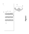
- FIG. 2 illustrates a top-down view of the substrate 112 in accordance with various embodiments.
- the thermal via structures 120 as shown in FIG. 2 , include surface features 204 .
- Callout 208 illustrates a magnified surface feature 204 for ease of description.
- the thermal via structures 120 are shown with a major dimension 212 and an orthogonal minor dimension 216 .
- a length of a thermal via structure 120 may be measured along its major dimension 212
- a width of the thermal via structure 120 may be measured along its minor dimension 216 .
- the width may be 125 microns
- the length may be between approximately 125 microns to 1 millimeter.
- the thermal via structure 120 may have a generally circular shape.
- the surface features 204 may each have a dimension 220 , which is parallel with the minor dimension 216 of the thermal via structure, and a dimension 224 , which is parallel with the major dimension 212 .
- the dimension 220 may be in a range of approximately 1-30 microns in some embodiments, while the dimension 224 may be in a range of approximately 1-60 microns. In some embodiments, a particularly effective range may be greater than approximately 10 microns for dimension 220 and greater than approximately 20 microns for dimension 224 .
- Providing surface features 204 may provide a locking mechanism between the thermal via structure 120 and an interior cavity surface of the substrate 112 .
- the locking mechanism may, in turn, provide the substrate 112 with mechanical stability to better withstand stresses that may be caused, e.g., by thermal cycling of the IC device 100 during operation.
- the locking mechanism may further enable the length and/or width of the thermal via structures 120 to be increased beyond that of convention thermal via bars. This may improve thermal transfer characteristics of the thermal via structures 120 and/or may provide for improved electrical characteristics with respect to the power/ground interface provided to the electronic component 108 by the thermal via structures 120 .
- the surface features 204 of the thermal via structures 120 may be tailored to meet specific requirements of the substrate 112 .
- a device may include surface features 204 having different shapes and/or dimensions depending on what portion of the thermal via structure 120 they are situated.
- thermal via structures 120 may include thermal via structures alternatively/additional disposed in other components.
- thermal via structures may be included in the electronic component 108 , the board 116 , and/or another component, e.g., heat sink.
- the dimensions of the thermal via structure and surface features may be proportionally adjusted in order to meet specific objectives of the environment in which they are disposed.
- FIGS. 3( a )- 3 ( c ) illustrate top-down views of substrates having thermal via structures with various patterns in accordance with some embodiments.
- FIG. 3( a ) illustrates a cross-section view of substrate 300 having thermal via structures 304 with arc-shaped patterns.
- FIG. 3( b ) illustrates a top-down view of a substrate 308 having thermal via structures 312 with sawtooth-shaped patterns.
- FIG. 3( c ) illustrates a top-down view of a substrate 316 having thermal via structures 320 with square-shaped patterns.
- Surface features of each of these thermal via structures may include dimensions that are similar to the surface-feature dimensions discussed above.
- the substrates 300 , 308 , 316 may be interchangeable with substrate 112 .
- FIG. 4 is a flowchart depicting a manufacturing operation 400 in accordance with some embodiments.
- the manufacturing operation 400 may be used to construct substrate 100 , 300 , 308 , or 316 .
- the manufacturing operation 400 may include, at block 404 , providing a substrate.
- the provided substrate may be manufactured by various manufacturing operations such as, but not limited to, patterning, depositing, laminating, planarizing, etc.
- various electrical connections may be formed in the provided substrate.
- the manufacturing operation 400 may include, at block 408 , forming cavities in the substrate.
- the cavities may be formed in the substrate through various manufacturing operations such as, but not limited to, laser drilling, mechanical drilling, etching, photoresist, punching, etc.
- the cavities may be provided with a shape that is to define the thermal via structures.
- the manufacturing operation 400 may include, at block 412 , forming the thermal via structures within the cavities of the substrate.
- the thermal via structures may be formed by providing thermally-conductive material in the cavities through any of various manufacturing operations including, but not limited to, plating, printing, depositing, etc.
- the shape of the surface features may assist with the efficiency of forming the thermal via structures.
- the edges of the cavities may increase surface tension, which may, in turn facilitate a plating process by, e.g., reducing the number of plating/grinding runs used. This may result in less material, e.g., copper, being used in the plating process and it may also decrease an amount of time required to form the thermal via structures.
- the increased surface tension provided by the edges of the cavities may also facilitate formation of larger thermal via structures, both in terms of length and width.
- Embodiments of an IC device may be incorporated into various other apparatuses and systems.
- a block diagram of an example system 500 is illustrated in FIG. 5 .
- the system 500 includes a power amplifier (PA) module 502 , which may be a radio frequency (RF) PA module in some embodiments.
- the system 500 may include a transceiver 504 coupled with the PA module 502 as illustrated.
- the PA module 502 may include an IC device (e.g., the IC device 100 ) to perform any of a variety of operations such as amplification, switching, mixing, etc.
- an IC device e.g., IC device 100
- an IC device may additionally/alternatively be included in the transceiver 504 to provide, e.g., up-converting.
- the PA module 502 may receive an RF input signal, RFin, from the transceiver 504 .
- the PA module 502 may amplify the RF input signal, RFin, to provide the RF output signal, RFout.
- the RF input signal, RFin, and the RF output signal, RFout may both be part of a transmit chain, respectively noted by Tx-RFin and Tx-RFout in FIG. 5 .
- the amplified RF output signal, RFout may be provided to an antenna switch module (ASM) 506 , which effectuates an over-the-air (OTA) transmission of the RF output signal, RFout, via an antenna structure 508 .
- ASM 506 may also receive RF signals via the antenna structure 508 and couple the received RF signals, Rx, to the transceiver 504 along a receive chain.
- the antenna structure 508 may include one or more directional and/or omnidirectional antennas, including, e.g., a dipole antenna, a monopole antenna, a patch antenna, a loop antenna, a microstrip antenna or any other type of antenna suitable for OTA transmission/reception of RF signals.
- the system 500 may be any system including power amplification. In various embodiments, inclusion of thermally-efficient IC device 100 in the system 500 may be particularly useful when the system 500 is used for power amplification at high RF power and frequency.
- the system 500 may be suitable for any one or more of terrestrial and satellite communications, radar systems, and possibly in various industrial and medical applications. More specifically, in various embodiments, the system 500 may be a selected one of a radar device, a satellite communication device, a mobile computing device (e.g., a phone, a tablet, a laptop, etc.), a base station, a broadcast radio, or a television amplifier system.
Abstract
Description
Claims (19)
Priority Applications (1)
| Application Number | Priority Date | Filing Date | Title |
|---|---|---|---|
| US13/476,923 US8908383B1 (en) | 2012-05-21 | 2012-05-21 | Thermal via structures with surface features |
Applications Claiming Priority (1)
| Application Number | Priority Date | Filing Date | Title |
|---|---|---|---|
| US13/476,923 US8908383B1 (en) | 2012-05-21 | 2012-05-21 | Thermal via structures with surface features |
Publications (1)
| Publication Number | Publication Date |
|---|---|
| US8908383B1 true US8908383B1 (en) | 2014-12-09 |
Family
ID=52001698
Family Applications (1)
| Application Number | Title | Priority Date | Filing Date |
|---|---|---|---|
| US13/476,923 Active 2032-10-24 US8908383B1 (en) | 2012-05-21 | 2012-05-21 | Thermal via structures with surface features |
Country Status (1)
| Country | Link |
|---|---|
| US (1) | US8908383B1 (en) |
Cited By (8)
| Publication number | Priority date | Publication date | Assignee | Title |
|---|---|---|---|---|
| US20160192471A1 (en) * | 2014-12-29 | 2016-06-30 | Samsung Electro-Mechanics Co., Ltd. | Circuit board and manufacturing method thereof |
| JPWO2014207815A1 (en) * | 2013-06-25 | 2017-02-23 | 株式会社メイコー | Heat dissipation board and manufacturing method thereof |
| WO2017105703A1 (en) * | 2015-12-15 | 2017-06-22 | Intel Corporation | Electronic package that includes finned vias |
| US20180092198A1 (en) * | 2015-04-13 | 2018-03-29 | Commissariat A L'energie Atomique Et Aux Energies Alternatives | Device for heating and cooling by a printed circuit for regenerating electronic components subjected to radiation |
| US10327325B2 (en) | 2015-07-06 | 2019-06-18 | ZK W Group GmbH | Printed circuit board and method for producing a printed circuit board |
| WO2020219119A1 (en) * | 2019-04-22 | 2020-10-29 | Raytheon Company | Mmic assembly |
| US11470714B2 (en) | 2019-10-23 | 2022-10-11 | At&S (China) Co. Ltd. | Component carrier with embedded component and horizontally elongated via |
| US11488889B1 (en) | 2017-08-08 | 2022-11-01 | Northrop Grumman Systems Corporation | Semiconductor device passive thermal management |
Citations (10)
| Publication number | Priority date | Publication date | Assignee | Title |
|---|---|---|---|---|
| US5506755A (en) | 1992-03-11 | 1996-04-09 | Kabushiki Kaisha Toshiba | Multi-layer substrate |
| US6124643A (en) * | 1997-01-28 | 2000-09-26 | Micron Technology, Inc. | Device assembly facilitating gap filling between spaced layers of semiconductor substrates |
| US20020172025A1 (en) * | 2000-11-15 | 2002-11-21 | Mohamed Megahed | Structure and method for fabrication of a leadless chip carrier with embedded inductor |
| US20050254215A1 (en) * | 2004-05-11 | 2005-11-17 | Michael Khbeis | Use of thermally conductive vias to extract heat from microelectronic chips and method of manufacturing |
| US7505275B2 (en) | 2005-11-04 | 2009-03-17 | Graftech International Holdings Inc. | LED with integral via |
| US20090146295A1 (en) * | 2007-12-11 | 2009-06-11 | Hidefumi Narita | Ceramic substrate having thermal via |
| US20090195334A1 (en) * | 2008-01-31 | 2009-08-06 | Tdk Corporation | High frequency module provided with power amplifier |
| US20090273002A1 (en) * | 2008-05-05 | 2009-11-05 | Wen-Chih Chiou | LED Package Structure and Fabrication Method |
| US20090278162A1 (en) * | 2005-09-01 | 2009-11-12 | E.I. Du Pont De Nemours And Company | Low Temperature Co-Fired Ceramic (LTCC) Tape Compositions, Light-Emitting Diode (LED) Modules, Lighting Devices and Methods of Forming Thereof |
| US20120007132A1 (en) * | 2010-07-08 | 2012-01-12 | Taiwan Semiconductor Manufacturing Company, Ltd. | Reduction of etch microloading for through silicon vias |
-
2012
- 2012-05-21 US US13/476,923 patent/US8908383B1/en active Active
Patent Citations (10)
| Publication number | Priority date | Publication date | Assignee | Title |
|---|---|---|---|---|
| US5506755A (en) | 1992-03-11 | 1996-04-09 | Kabushiki Kaisha Toshiba | Multi-layer substrate |
| US6124643A (en) * | 1997-01-28 | 2000-09-26 | Micron Technology, Inc. | Device assembly facilitating gap filling between spaced layers of semiconductor substrates |
| US20020172025A1 (en) * | 2000-11-15 | 2002-11-21 | Mohamed Megahed | Structure and method for fabrication of a leadless chip carrier with embedded inductor |
| US20050254215A1 (en) * | 2004-05-11 | 2005-11-17 | Michael Khbeis | Use of thermally conductive vias to extract heat from microelectronic chips and method of manufacturing |
| US20090278162A1 (en) * | 2005-09-01 | 2009-11-12 | E.I. Du Pont De Nemours And Company | Low Temperature Co-Fired Ceramic (LTCC) Tape Compositions, Light-Emitting Diode (LED) Modules, Lighting Devices and Methods of Forming Thereof |
| US7505275B2 (en) | 2005-11-04 | 2009-03-17 | Graftech International Holdings Inc. | LED with integral via |
| US20090146295A1 (en) * | 2007-12-11 | 2009-06-11 | Hidefumi Narita | Ceramic substrate having thermal via |
| US20090195334A1 (en) * | 2008-01-31 | 2009-08-06 | Tdk Corporation | High frequency module provided with power amplifier |
| US20090273002A1 (en) * | 2008-05-05 | 2009-11-05 | Wen-Chih Chiou | LED Package Structure and Fabrication Method |
| US20120007132A1 (en) * | 2010-07-08 | 2012-01-12 | Taiwan Semiconductor Manufacturing Company, Ltd. | Reduction of etch microloading for through silicon vias |
Cited By (13)
| Publication number | Priority date | Publication date | Assignee | Title |
|---|---|---|---|---|
| JPWO2014207815A1 (en) * | 2013-06-25 | 2017-02-23 | 株式会社メイコー | Heat dissipation board and manufacturing method thereof |
| US10064291B2 (en) * | 2014-12-29 | 2018-08-28 | Samsung Electro-Mechanics Co., Ltd. | Circuit board and manufacturing method thereof |
| US20160192471A1 (en) * | 2014-12-29 | 2016-06-30 | Samsung Electro-Mechanics Co., Ltd. | Circuit board and manufacturing method thereof |
| US10791619B2 (en) * | 2015-04-13 | 2020-09-29 | Commissariat A L'energie Atomique Et Aux Energies Alternatives | Device for heating and cooling by a printed circuit for regenerating electronic components subjected to radiation |
| US20180092198A1 (en) * | 2015-04-13 | 2018-03-29 | Commissariat A L'energie Atomique Et Aux Energies Alternatives | Device for heating and cooling by a printed circuit for regenerating electronic components subjected to radiation |
| US10327325B2 (en) | 2015-07-06 | 2019-06-18 | ZK W Group GmbH | Printed circuit board and method for producing a printed circuit board |
| US9795026B2 (en) * | 2015-12-15 | 2017-10-17 | Intel Corporation | Electronic package that includes finned vias |
| CN108292636A (en) * | 2015-12-15 | 2018-07-17 | 英特尔公司 | Include the Electronic Packaging of fin via |
| WO2017105703A1 (en) * | 2015-12-15 | 2017-06-22 | Intel Corporation | Electronic package that includes finned vias |
| US11488889B1 (en) | 2017-08-08 | 2022-11-01 | Northrop Grumman Systems Corporation | Semiconductor device passive thermal management |
| WO2020219119A1 (en) * | 2019-04-22 | 2020-10-29 | Raytheon Company | Mmic assembly |
| US10896861B2 (en) | 2019-04-22 | 2021-01-19 | Raytheon Company | Heterogeneous multi-layer MMIC assembly |
| US11470714B2 (en) | 2019-10-23 | 2022-10-11 | At&S (China) Co. Ltd. | Component carrier with embedded component and horizontally elongated via |
Similar Documents
| Publication | Publication Date | Title |
|---|---|---|
| US8908383B1 (en) | Thermal via structures with surface features | |
| US20200412858A1 (en) | Microelectronic devices designed with integrated antennas on a substrate | |
| US11870132B2 (en) | Antenna modules and communication devices | |
| US8952521B2 (en) | Semiconductor packages with integrated antenna and method of forming thereof | |
| US8648454B2 (en) | Wafer-scale package structures with integrated antennas | |
| US11336015B2 (en) | Antenna boards and communication devices | |
| Samanta | Pushing the envelope for heterogeneity: Multilayer and 3-D heterogeneous integrations for next generation millimeter-and submillimeter-wave circuits and systems | |
| US20130308274A1 (en) | Thermal spreader having graduated thermal expansion parameters | |
| Bhutani et al. | Packaging solution based on low-temperature cofired ceramic technology for frequencies beyond 100 GHz | |
| US9559034B2 (en) | Package for high-power semiconductor devices | |
| US20180331051A1 (en) | Microelectronic devices designed with high frequency communication devices including compound semiconductor devices integrated on a die fabric on package | |
| US20170347490A1 (en) | High-frequency antenna structure with high thermal conductivity and high surface area | |
| US11600932B2 (en) | Antenna-on-package including multiple types of antenna | |
| US20210041182A1 (en) | Thermal management in integrated circuit packages | |
| US11303009B2 (en) | Packages for advanced antenna systems | |
| Zhang et al. | Fan-out Antenna-in-Package integration using heatsink antenna | |
| US9585240B2 (en) | Advanced grounding scheme | |
| US20100123228A1 (en) | Package including proximately-positioned lead frame | |
| Hamidipour et al. | Antennas in package with stacked metallization | |
| EP4160668A1 (en) | Leadless power amplifier package including topside termination arrangements | |
| US6933603B2 (en) | Multi-substrate layer semiconductor packages and method for making same | |
| Pavlidis et al. | A 5.4 W X-band gallium nitride (GaN) power amplifier in an encapsulated organic package | |
| Kimura et al. | An X-band high power tile-type GaN TR module for low-profile AESA | |
| Hu et al. | Advanced development in packaging of antenna-integrated systems for millimeter-wave applications | |
| CN220569668U (en) | Electronic device |
Legal Events
| Date | Code | Title | Description |
|---|---|---|---|
| AS | Assignment |
Owner name: TRIQUINT SEMICONDUCTOR, INC., OREGON Free format text: ASSIGNMENT OF ASSIGNORS INTEREST;ASSIGNORS:RAILKAR, TARAK A.;BANTZ, PAUL D.;SIGNING DATES FROM 20120517 TO 20120518;REEL/FRAME:028259/0313 |
|
| STCF | Information on status: patent grant |
Free format text: PATENTED CASE |
|
| AS | Assignment |
Owner name: QORVO US, INC., NORTH CAROLINA Free format text: MERGER;ASSIGNOR:TRIQUINT SEMICONDUCTOR, INC.;REEL/FRAME:039050/0193 Effective date: 20160330 |
|
| FEPP | Fee payment procedure |
Free format text: MAINTENANCE FEE REMINDER MAILED (ORIGINAL EVENT CODE: REM.) |
|
| FEPP | Fee payment procedure |
Free format text: SURCHARGE FOR LATE PAYMENT, LARGE ENTITY (ORIGINAL EVENT CODE: M1554); ENTITY STATUS OF PATENT OWNER: LARGE ENTITY |
|
| MAFP | Maintenance fee payment |
Free format text: PAYMENT OF MAINTENANCE FEE, 4TH YEAR, LARGE ENTITY (ORIGINAL EVENT CODE: M1551); ENTITY STATUS OF PATENT OWNER: LARGE ENTITY Year of fee payment: 4 |
|
| MAFP | Maintenance fee payment |
Free format text: PAYMENT OF MAINTENANCE FEE, 8TH YEAR, LARGE ENTITY (ORIGINAL EVENT CODE: M1552); ENTITY STATUS OF PATENT OWNER: LARGE ENTITY Year of fee payment: 8 |