US8916825B1 - Ultraviolet, infrared and terahertz photo/radiation sensors using graphene layers to enhance sensitivity - Google Patents
Ultraviolet, infrared and terahertz photo/radiation sensors using graphene layers to enhance sensitivity Download PDFInfo
- Publication number
- US8916825B1 US8916825B1 US13/308,688 US201113308688A US8916825B1 US 8916825 B1 US8916825 B1 US 8916825B1 US 201113308688 A US201113308688 A US 201113308688A US 8916825 B1 US8916825 B1 US 8916825B1
- Authority
- US
- United States
- Prior art keywords
- graphene
- thin film
- detector
- carbon nanotubes
- radiation
- Prior art date
- Legal status (The legal status is an assumption and is not a legal conclusion. Google has not performed a legal analysis and makes no representation as to the accuracy of the status listed.)
- Active
Links
- OKTJSMMVPCPJKN-UHFFFAOYSA-N Carbon Chemical compound [C] OKTJSMMVPCPJKN-UHFFFAOYSA-N 0.000 title claims abstract description 102
- 229910021389 graphene Inorganic materials 0.000 title claims abstract description 91
- 230000005855 radiation Effects 0.000 title claims abstract description 19
- 230000035945 sensitivity Effects 0.000 title claims abstract description 4
- 238000000034 method Methods 0.000 claims abstract description 37
- 239000000758 substrate Substances 0.000 claims abstract description 16
- 238000004891 communication Methods 0.000 claims abstract description 5
- 238000007306 functionalization reaction Methods 0.000 claims abstract 2
- 239000010409 thin film Substances 0.000 claims description 15
- 239000010408 film Substances 0.000 claims description 14
- 239000002041 carbon nanotube Substances 0.000 claims description 12
- 229910021393 carbon nanotube Inorganic materials 0.000 claims description 11
- 239000002109 single walled nanotube Substances 0.000 claims description 5
- 238000002955 isolation Methods 0.000 claims description 4
- 239000002048 multi walled nanotube Substances 0.000 claims description 3
- 229910052581 Si3N4 Inorganic materials 0.000 claims 1
- 239000003989 dielectric material Substances 0.000 claims 1
- HQVNEWCFYHHQES-UHFFFAOYSA-N silicon nitride Chemical compound N12[Si]34N5[Si]62N3[Si]51N64 HQVNEWCFYHHQES-UHFFFAOYSA-N 0.000 claims 1
- 239000010410 layer Substances 0.000 abstract description 48
- 238000010521 absorption reaction Methods 0.000 abstract description 19
- VYPSYNLAJGMNEJ-UHFFFAOYSA-N Silicium dioxide Chemical compound O=[Si]=O VYPSYNLAJGMNEJ-UHFFFAOYSA-N 0.000 abstract description 11
- 239000002184 metal Substances 0.000 abstract description 11
- 239000002074 nanoribbon Substances 0.000 abstract description 11
- 229910052751 metal Inorganic materials 0.000 abstract description 10
- 239000002356 single layer Substances 0.000 abstract description 3
- 229910052681 coesite Inorganic materials 0.000 abstract description 2
- 229910052906 cristobalite Inorganic materials 0.000 abstract description 2
- 239000000377 silicon dioxide Substances 0.000 abstract description 2
- 235000012239 silicon dioxide Nutrition 0.000 abstract description 2
- 229910052682 stishovite Inorganic materials 0.000 abstract description 2
- 229910052905 tridymite Inorganic materials 0.000 abstract description 2
- 239000002365 multiple layer Substances 0.000 abstract 1
- 238000010586 diagram Methods 0.000 description 29
- 239000004744 fabric Substances 0.000 description 22
- 238000004519 manufacturing process Methods 0.000 description 19
- 239000002071 nanotube Substances 0.000 description 17
- 239000000463 material Substances 0.000 description 15
- 239000004065 semiconductor Substances 0.000 description 14
- 238000001514 detection method Methods 0.000 description 11
- 230000008569 process Effects 0.000 description 10
- 229910021417 amorphous silicon Inorganic materials 0.000 description 9
- KDLHZDBZIXYQEI-UHFFFAOYSA-N Palladium Chemical compound [Pd] KDLHZDBZIXYQEI-UHFFFAOYSA-N 0.000 description 8
- 238000005516 engineering process Methods 0.000 description 8
- 229910052721 tungsten Inorganic materials 0.000 description 8
- 238000003491 array Methods 0.000 description 7
- 229920002120 photoresistant polymer Polymers 0.000 description 7
- BASFCYQUMIYNBI-UHFFFAOYSA-N platinum Chemical compound [Pt] BASFCYQUMIYNBI-UHFFFAOYSA-N 0.000 description 7
- 229910052814 silicon oxide Inorganic materials 0.000 description 7
- XUIMIQQOPSSXEZ-UHFFFAOYSA-N Silicon Chemical compound [Si] XUIMIQQOPSSXEZ-UHFFFAOYSA-N 0.000 description 6
- 239000010949 copper Substances 0.000 description 6
- 229910052710 silicon Inorganic materials 0.000 description 6
- 239000010703 silicon Substances 0.000 description 6
- WFKWXMTUELFFGS-UHFFFAOYSA-N tungsten Chemical compound [W] WFKWXMTUELFFGS-UHFFFAOYSA-N 0.000 description 6
- 239000010937 tungsten Substances 0.000 description 6
- 230000000694 effects Effects 0.000 description 5
- 230000005670 electromagnetic radiation Effects 0.000 description 5
- 238000005457 optimization Methods 0.000 description 5
- 238000012545 processing Methods 0.000 description 5
- 229910001218 Gallium arsenide Inorganic materials 0.000 description 4
- 229910052802 copper Inorganic materials 0.000 description 4
- 238000013461 design Methods 0.000 description 4
- 238000004377 microelectronic Methods 0.000 description 4
- 230000003287 optical effect Effects 0.000 description 4
- 229910052763 palladium Inorganic materials 0.000 description 4
- 238000000206 photolithography Methods 0.000 description 4
- 229910052697 platinum Inorganic materials 0.000 description 4
- 235000012431 wafers Nutrition 0.000 description 4
- XHCLAFWTIXFWPH-UHFFFAOYSA-N [O-2].[O-2].[O-2].[O-2].[O-2].[V+5].[V+5] Chemical compound [O-2].[O-2].[O-2].[O-2].[O-2].[V+5].[V+5] XHCLAFWTIXFWPH-UHFFFAOYSA-N 0.000 description 3
- 229910052782 aluminium Inorganic materials 0.000 description 3
- 230000003321 amplification Effects 0.000 description 3
- 238000003199 nucleic acid amplification method Methods 0.000 description 3
- 229910001935 vanadium oxide Inorganic materials 0.000 description 3
- RYGMFSIKBFXOCR-UHFFFAOYSA-N Copper Chemical compound [Cu] RYGMFSIKBFXOCR-UHFFFAOYSA-N 0.000 description 2
- 229910005540 GaP Inorganic materials 0.000 description 2
- WPPDFTBPZNZZRP-UHFFFAOYSA-N aluminum copper Chemical compound [Al].[Cu] WPPDFTBPZNZZRP-UHFFFAOYSA-N 0.000 description 2
- 230000008901 benefit Effects 0.000 description 2
- 239000000969 carrier Substances 0.000 description 2
- 230000005284 excitation Effects 0.000 description 2
- 230000010354 integration Effects 0.000 description 2
- 238000001459 lithography Methods 0.000 description 2
- 229910044991 metal oxide Inorganic materials 0.000 description 2
- 238000005272 metallurgy Methods 0.000 description 2
- 150000002739 metals Chemical class 0.000 description 2
- 230000037230 mobility Effects 0.000 description 2
- 239000002059 nanofabric Substances 0.000 description 2
- 238000000059 patterning Methods 0.000 description 2
- 238000005498 polishing Methods 0.000 description 2
- 230000008054 signal transmission Effects 0.000 description 2
- 238000004544 sputter deposition Methods 0.000 description 2
- BLIQUJLAJXRXSG-UHFFFAOYSA-N 1-benzyl-3-(trifluoromethyl)pyrrolidin-1-ium-3-carboxylate Chemical compound C1C(C(=O)O)(C(F)(F)F)CCN1CC1=CC=CC=C1 BLIQUJLAJXRXSG-UHFFFAOYSA-N 0.000 description 1
- VLJQDHDVZJXNQL-UHFFFAOYSA-N 4-methyl-n-(oxomethylidene)benzenesulfonamide Chemical compound CC1=CC=C(S(=O)(=O)N=C=O)C=C1 VLJQDHDVZJXNQL-UHFFFAOYSA-N 0.000 description 1
- 229910017083 AlN Inorganic materials 0.000 description 1
- 229910000980 Aluminium gallium arsenide Inorganic materials 0.000 description 1
- 230000005457 Black-body radiation Effects 0.000 description 1
- 229910004613 CdTe Inorganic materials 0.000 description 1
- 229910019044 CoSix Inorganic materials 0.000 description 1
- 229910002601 GaN Inorganic materials 0.000 description 1
- UFHFLCQGNIYNRP-UHFFFAOYSA-N Hydrogen Chemical compound [H][H] UFHFLCQGNIYNRP-UHFFFAOYSA-N 0.000 description 1
- 229910000673 Indium arsenide Inorganic materials 0.000 description 1
- 229910020968 MoSi2 Inorganic materials 0.000 description 1
- 229910005889 NiSix Inorganic materials 0.000 description 1
- -1 RuN Inorganic materials 0.000 description 1
- 229910000577 Silicon-germanium Inorganic materials 0.000 description 1
- 229910004166 TaN Inorganic materials 0.000 description 1
- 229910010037 TiAlN Inorganic materials 0.000 description 1
- 229910008486 TiSix Inorganic materials 0.000 description 1
- 229910008599 TiW Inorganic materials 0.000 description 1
- ATJFFYVFTNAWJD-UHFFFAOYSA-N Tin Chemical compound [Sn] ATJFFYVFTNAWJD-UHFFFAOYSA-N 0.000 description 1
- 229910008814 WSi2 Inorganic materials 0.000 description 1
- 238000007792 addition Methods 0.000 description 1
- XAGFODPZIPBFFR-UHFFFAOYSA-N aluminium Chemical compound [Al] XAGFODPZIPBFFR-UHFFFAOYSA-N 0.000 description 1
- 238000013459 approach Methods 0.000 description 1
- 239000003125 aqueous solvent Substances 0.000 description 1
- QVGXLLKOCUKJST-UHFFFAOYSA-N atomic oxygen Chemical compound [O] QVGXLLKOCUKJST-UHFFFAOYSA-N 0.000 description 1
- 230000004888 barrier function Effects 0.000 description 1
- 230000005540 biological transmission Effects 0.000 description 1
- 238000006243 chemical reaction Methods 0.000 description 1
- 150000001875 compounds Chemical class 0.000 description 1
- 239000004020 conductor Substances 0.000 description 1
- 238000001816 cooling Methods 0.000 description 1
- 239000013078 crystal Substances 0.000 description 1
- 230000007547 defect Effects 0.000 description 1
- 238000013400 design of experiment Methods 0.000 description 1
- 229910003460 diamond Inorganic materials 0.000 description 1
- 239000010432 diamond Substances 0.000 description 1
- 238000007599 discharging Methods 0.000 description 1
- 239000003792 electrolyte Substances 0.000 description 1
- 238000005566 electron beam evaporation Methods 0.000 description 1
- 230000008030 elimination Effects 0.000 description 1
- 238000003379 elimination reaction Methods 0.000 description 1
- 238000005530 etching Methods 0.000 description 1
- 239000000835 fiber Substances 0.000 description 1
- 230000005669 field effect Effects 0.000 description 1
- 238000010438 heat treatment Methods 0.000 description 1
- 229910052739 hydrogen Inorganic materials 0.000 description 1
- 239000001257 hydrogen Substances 0.000 description 1
- 150000002483 hydrogen compounds Chemical class 0.000 description 1
- 238000005286 illumination Methods 0.000 description 1
- RPQDHPTXJYYUPQ-UHFFFAOYSA-N indium arsenide Chemical compound [In]#[As] RPQDHPTXJYYUPQ-UHFFFAOYSA-N 0.000 description 1
- 230000000977 initiatory effect Effects 0.000 description 1
- 238000002347 injection Methods 0.000 description 1
- 239000007924 injection Substances 0.000 description 1
- 239000012212 insulator Substances 0.000 description 1
- 150000002500 ions Chemical class 0.000 description 1
- 230000031700 light absorption Effects 0.000 description 1
- 150000004706 metal oxides Chemical class 0.000 description 1
- VNWKTOKETHGBQD-UHFFFAOYSA-N methane Chemical compound C VNWKTOKETHGBQD-UHFFFAOYSA-N 0.000 description 1
- 238000012986 modification Methods 0.000 description 1
- 230000004048 modification Effects 0.000 description 1
- 229910003465 moissanite Inorganic materials 0.000 description 1
- 229910052750 molybdenum Inorganic materials 0.000 description 1
- 229910052759 nickel Inorganic materials 0.000 description 1
- 238000012634 optical imaging Methods 0.000 description 1
- 230000005693 optoelectronics Effects 0.000 description 1
- 239000003960 organic solvent Substances 0.000 description 1
- 229910052760 oxygen Inorganic materials 0.000 description 1
- 239000001301 oxygen Substances 0.000 description 1
- 238000002161 passivation Methods 0.000 description 1
- 230000035515 penetration Effects 0.000 description 1
- 230000000704 physical effect Effects 0.000 description 1
- 238000001020 plasma etching Methods 0.000 description 1
- 229910021340 platinum monosilicide Inorganic materials 0.000 description 1
- 229910010271 silicon carbide Inorganic materials 0.000 description 1
- 239000000243 solution Substances 0.000 description 1
- 229910052715 tantalum Inorganic materials 0.000 description 1
- 238000012360 testing method Methods 0.000 description 1
- 229910052718 tin Inorganic materials 0.000 description 1
- 229910052719 titanium Inorganic materials 0.000 description 1
Images


Classifications
-
- H—ELECTRICITY
- H10—SEMICONDUCTOR DEVICES; ELECTRIC SOLID-STATE DEVICES NOT OTHERWISE PROVIDED FOR
- H10K—ORGANIC ELECTRIC SOLID-STATE DEVICES
- H10K85/00—Organic materials used in the body or electrodes of devices covered by this subclass
- H10K85/20—Carbon compounds, e.g. carbon nanotubes or fullerenes
- H10K85/221—Carbon nanotubes
-
- G—PHYSICS
- G01—MEASURING; TESTING
- G01J—MEASUREMENT OF INTENSITY, VELOCITY, SPECTRAL CONTENT, POLARISATION, PHASE OR PULSE CHARACTERISTICS OF INFRARED, VISIBLE OR ULTRAVIOLET LIGHT; COLORIMETRY; RADIATION PYROMETRY
- G01J5/00—Radiation pyrometry, e.g. infrared or optical thermometry
- G01J5/02—Constructional details
- G01J5/0225—Shape of the cavity itself or of elements contained in or suspended over the cavity
- G01J5/024—Special manufacturing steps or sacrificial layers or layer structures
-
- G—PHYSICS
- G01—MEASURING; TESTING
- G01J—MEASUREMENT OF INTENSITY, VELOCITY, SPECTRAL CONTENT, POLARISATION, PHASE OR PULSE CHARACTERISTICS OF INFRARED, VISIBLE OR ULTRAVIOLET LIGHT; COLORIMETRY; RADIATION PYROMETRY
- G01J5/00—Radiation pyrometry, e.g. infrared or optical thermometry
- G01J5/02—Constructional details
- G01J5/04—Casings
- G01J5/046—Materials; Selection of thermal materials
-
- G—PHYSICS
- G01—MEASURING; TESTING
- G01J—MEASUREMENT OF INTENSITY, VELOCITY, SPECTRAL CONTENT, POLARISATION, PHASE OR PULSE CHARACTERISTICS OF INFRARED, VISIBLE OR ULTRAVIOLET LIGHT; COLORIMETRY; RADIATION PYROMETRY
- G01J5/00—Radiation pyrometry, e.g. infrared or optical thermometry
- G01J5/10—Radiation pyrometry, e.g. infrared or optical thermometry using electric radiation detectors
- G01J5/20—Radiation pyrometry, e.g. infrared or optical thermometry using electric radiation detectors using resistors, thermistors or semiconductors sensitive to radiation, e.g. photoconductive devices
- G01J5/22—Electrical features thereof
- G01J5/24—Use of specially adapted circuits, e.g. bridge circuits
-
- H—ELECTRICITY
- H10—SEMICONDUCTOR DEVICES; ELECTRIC SOLID-STATE DEVICES NOT OTHERWISE PROVIDED FOR
- H10K—ORGANIC ELECTRIC SOLID-STATE DEVICES
- H10K30/00—Organic devices sensitive to infrared radiation, light, electromagnetic radiation of shorter wavelength or corpuscular radiation
- H10K30/60—Organic devices sensitive to infrared radiation, light, electromagnetic radiation of shorter wavelength or corpuscular radiation in which radiation controls flow of current through the devices, e.g. photoresistors
- H10K30/65—Light-sensitive field-effect devices, e.g. phototransistors
-
- H—ELECTRICITY
- H10—SEMICONDUCTOR DEVICES; ELECTRIC SOLID-STATE DEVICES NOT OTHERWISE PROVIDED FOR
- H10K—ORGANIC ELECTRIC SOLID-STATE DEVICES
- H10K30/00—Organic devices sensitive to infrared radiation, light, electromagnetic radiation of shorter wavelength or corpuscular radiation
- H10K30/80—Constructional details
- H10K30/81—Electrodes
-
- H—ELECTRICITY
- H10—SEMICONDUCTOR DEVICES; ELECTRIC SOLID-STATE DEVICES NOT OTHERWISE PROVIDED FOR
- H10K—ORGANIC ELECTRIC SOLID-STATE DEVICES
- H10K39/00—Integrated devices, or assemblies of multiple devices, comprising at least one organic radiation-sensitive element covered by group H10K30/00
- H10K39/30—Devices controlled by radiation
-
- H—ELECTRICITY
- H10—SEMICONDUCTOR DEVICES; ELECTRIC SOLID-STATE DEVICES NOT OTHERWISE PROVIDED FOR
- H10K—ORGANIC ELECTRIC SOLID-STATE DEVICES
- H10K71/00—Manufacture or treatment specially adapted for the organic devices covered by this subclass
- H10K71/20—Changing the shape of the active layer in the devices, e.g. patterning
- H10K71/231—Changing the shape of the active layer in the devices, e.g. patterning by etching of existing layers
Definitions
- the present application relates generally to bundled nanotube fabrics and methods of making the same.
- Photodetectors are an integral part of optical circuits and components (for example emitters, modulators, repeaters, waveguides or fibers, reflectors, resonators, detectors, IR Focal plane arrays, UV microchannel arrays and THZ diode detectors etc.) and are used for the sensing of electromagnetic radiation.
- Photoconducting materials typically semiconductors, have electrical properties that vary when exposed to electromagnetic radiation (i.e. light).
- One type of photoconductivity arises from the generation of mobile carriers (electrons or holes) during absorption of photons.
- E g the materials band gap
- h Plank's constant (4.136 ⁇ 10 ⁇ 15 eVs)
- c the speed of light in a vacuum (2.998 ⁇ 10 10 cm/s)
- l the wavelength of the radiation
- Light detection is ideally suited for direct band gap semiconductors such as Ge and GaAs.
- indirect band gap semiconductors where an additional phonon energy is needed to excite an electron from the valence band to the conduction band
- photodetectors are also used as photodetectors.
- a widely known type of photodetectors is the solar cell, which uses a simple p-n diode or Schottky barrier to detect impinging photons.
- silicon most photodetectors disadvantageously do not integrate with existing microelectronics technology, usually detect only a specific wavelength (i.e. 1.1 mm for Si, 0.87 mm for GaAs, 0.414 mm for a-SiC and 1.89 mm for Ge), and require multiple detectors to detect a broad band of wavelengths (hence photon energy).
- Bolometers operate by absorbing radiation, which in turn raises the temperature of the material and hence alters the resistance of the material.
- Bolometers can be constructed from metallic, metallic-oxides or semiconducting materials such as vanadium oxide and amorphous silicon.
- bolometers detect a broad range of radiation above a few microns
- bolometers are typically thermally stabilized to reduce the possibility of detection of blackbody radiation that is emitted from the detector material, which leads to a high background noise.
- IR microbolometer detectors and arrays advantageously do not require cooling to cryogenic temperatures unlike the other detector technologies discussed.
- Typical band-gaps for carbon nanotubes range from approximately 0.6-1.2 eV, depending on the diameter of the CNT, where the band gap is proportional to the inverse diameter of the nanotube. These energies correlate to the ability of the nanotubes to detect radiation in the near IR range. Since nanotubes also generate heat and phonons by several processes (e.g., injection of electrons, impinging with radiation, etc.), a CNT fabric is also ideally suited as an IR detector.
- the nanoribbons can serve as either photodetectors or a microbolometer through modulation of the temperature coefficient of resistance of the graphene layer(s).
- An existing prior art microbolometer utilizes vanadium oxide as the element which changes impedance for incoming IR radiation. Typically 2% per degree C. is the highest thermal coefficient of resistance achievable. This performance is limited by 1/f noise and the basic physical properties of the vanadium oxide film.
- the VOx based micro bolometer is fabricated on top of the CMOS readout circuit, which provides a cost benefit.
- the present invention overcomes the disadvantages of the prior art by providing a light detector includes a single graphene layer or multiple layers article in electrical communication with a first and a second contact; and a detection circuit in electrical communication with the first and second contacts.
- the detection circuit provides electrical outputs for sufficient light detection from the nanotube article in the proximity of the predefined region by use of preamplification.
- the predefined region where graphene layer(s) are situated on a cantilever beam that provides thermal isolation from the surrounding environment is provided.
- the predefined region is between two electrical contacts. These electrical contacts provide electrical communication but also are designed for maximum thermal isolation.
- the use of Palladium or platinum is required to enhance pi bond connects in the graphene phase and the metal interconnects.
- the graphene based detector invention light detection arrays can be integrated with semiconductor circuits including CMOS circuits which provide pixel array x-y controls, pre-amplification of the modulated resistance signal from the IR detector and the conversion of the analog signal to digital.
- the graphene nanoribbon film(s) increase the temperature coefficient of resistance from state of the art of 0.025 per degree Centigrade to in excess of 0.04% per degree centigrade.
- the graphene based microbolometer detects light by resistance changes in the fabric due to heating.
- the IR detector no longer suffers from the Nyquist frequency limitation. This is due to the fact that the Nyquist frequency limitation is due to the presence of 1/f or flicker noise.
- the use of graphene ribbons exhibit non measurable noise sources, and thus the IR detector no longer suffers from the Nyquist frequency limitation.
- the elimination of Nyquist limited behavior significantly improves the performance of IR detection systems.
- FIG. 1 is a schematic diagram of a microbolometer detecting element according to an illustrative embodiment employing a graphene sensing element fabricated on a generic CMOS wafer process;
- FIG. 2A is a schematic diagram of the resulting structure after a first step is performed in fabrication of a graphene based IR detector, in which a film is deposited on a substrate and standard photolithography creates a hole over the tungsten (W) plugs, according to the illustrative embodiment;
- FIG. 2B is a schematic diagram of the resulting structure after another step is performed in the fabrication of the IR detector, in which a thin film of Cu is deposited, according to the illustrative embodiment
- FIG. 2C is a schematic diagram of the resulting structure after another step is performed in the fabrication of the IR detector, in which a layer of amorphous silicon is deposited, according to the illustrative embodiment
- FIG. 2D is a schematic diagram of the resulting structure after another step is performed in the fabrication of the IR detector, in which the layer of amorphous silicon is planarized using chemical-mechanical polishing, according to the illustrative embodiment;
- FIG. 2E is a schematic diagram of the resulting structure after another step is performed in the fabrication of the IR detector, in which contact holes are provided through the amorphous silicon and silicon oxide layers, thereby clearing the material down to the underlying tungsten (W) plus, according to the illustrative embodiment;
- FIG. 2F is a schematic diagram of the resulting structure after another step is performed in the fabrication of the IR detector, in which standard CMOS interconnect metallurgy is deposited, according to the illustrative embodiment
- FIG. 2G is a schematic diagram of the resulting structure after another step is performed in the fabrication of the IR detector, in which a graphene layer is deposited, according to the illustrative embodiment
- FIG. 2H is a schematic diagram of the resulting IR detector after the final step is performed in the fabrication of the IR detector, in which the graphene layer is masked off to create the image detector design desired and the amorphous silicon in the cavity is etched, according to the illustrative embodiment;
- FIG. 2I is a flow chart of a procedure for the fabrication of graphene from carbon nanotubes, according to the illustrative embodiment
- FIG. 3 is a perspective view of the fully assembled graphene based microbolometer, in accordance with an illustrative embodiment
- FIG. 4 is a top view of an array of graphene based microbolometers, in accordance with the illustrative embodiments
- FIG. 5 is a schematic diagram of the CMOS readout circuit for the graphene IR detector, in accordance with the illustrative embodiments
- FIG. 6 is a graphical diagram of the measured film resistance of a graphene layer versus temperature, according to the illustrative embodiment
- FIG. 7A is a schematic diagram of a photo-field effect transistor device structure incorporating a graphene layer or multilayer, in accordance with the illustrative embodiments.
- FIG. 7B is a band gap diagram of the structure of FIG. 7A , according to the illustrative embodiments.
- FIG. 8A is a graphical diagram of the Ultraviolet (UV) absorption of a graphene layer, according to the illustrative embodiments.
- FIG. 8B is a graphical diagram of the Infrared (IR) absorption of a graphene layer, according to the illustrative embodiments.
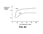
- FIG. 8C is a graphical diagram of the Terahertz (THZ) absorption of a graphene layer, according to the illustrative embodiments.
- IR radiation detectors can be employed as Infrared (IR) radiation detectors.
- the application of graphene single layer or multilayers on a thermally isolated cantilever beam can be employed as an IR radiation detector.
- One possible technique that can be used to detect electromagnetic radiation is a resistive type microbolometer that changes its electrical resistance as its temperature rises due to the absorption of electromagnetic radiation.
- Graphene based detectors have several important and unique features that are not available with existing technologies.
- arrays of these nanotube light detectors can be formed using patterning technology at minimum dimensions of the lithography node used or dictated by the demands of the optical imaging system. It is possible to create 25, 17, or 8 micron square or less detectors limited only by photolithography techniques.
- the fabrics can be composed of all multi-walled structures or of a combination of single- and multi-walled structures which are processed into graphene nanoribbons.
- Illustrative embodiments of the invention allow integration at a level of one light detector per ten or less transistors at the minimum dimension of a given lithography node or the integration of large arrays that are addressed by CMOS pre-amplification or readout and logic circuits.
- CMOS pre-amplification or readout and logic circuits Previously only discrete components, such as silicon p-n diodes, could be used as light detectors for optoelectronic circuits.
- Other types of detectors require complex and difficult fabrication techniques such as flip-chip processes to integrate with silicon semiconductor technology. Because CNT light sensors can be integrated to form VLSI arrays, which allows for optical interconnects having one light detector per transistor (or waveguide, depending on function), the fabrication of ultra-dense optical circuits is possible.
- FIG. 1 shows a schematic diagram of an IR detector having a graphene based fabric sensing element fabricated on a generic CMOS wafer.
- the IR detector incorporates a graphene based fabric sensing element for performing the infrared detection.
- the IR detector 100 includes a conventional P-N junction substrate 101 , which is part of the overall CMOS logic 110 .
- the substrate 101 can comprise silicon using a Bridgman float zone technique.
- the film 120 can comprise a silicon oxide layer based upon the absorption frequency for the type of device.
- the IR detector 101 is fabricated in accordance with the procedures outlined in FIGS. 2A through 21 .
- Light detectors can be constructed using suspended or non-suspended nanotube-based fabrics in combination with appropriate substrates. Fabrication techniques to develop such horizontally- and vertically-disposed fabrics and devices composed of nanotube fabrics which comprise redundant conducting nanotubes may be created via CVD, or by room temperature operations as described herein. For useful background material on fabrication of carbon nanotubes, refer to U.S. Pat. No. 6,706,402, and published PCT Application No. WO 01/03208, which are expressly incorporated by reference herein. Such detectors can be part of a scheme involving signal transmission or use in a display.
- the substrate material 101 can be an insulator such as one described hereinabove or can be a semiconductor (such as, but not limited to, Si (single crystal, polycrystalline and amorphous), Ge, SiGe, SiC, Diamond, GaN, GaAs, GaP, AlGaAs, InP, GaP, CdTe, AlN, InAs, Al x In 1-x P, and other III-V and II-VI semiconductors) or a conductor (such as, but not limited to, Al, Cu, W, Al( ⁇ 1% Cu), Co, Ti, Ta, W, Ni, Mo, Pd, Pt, TiW, Ru, CoSi x , WSi 2 , TiSi x , TaN, TiN, TiAlN, RuN, RuO, PtSi, Pd 2 Si, MoSi 2 , NiSi x ).
- a semiconductor such as, but not limited to, Si (single crystal, polycrystalline and amorphous), Ge, SiG
- the substrate material systems can be chosen for circuitry technologies and light absorption considerations, the graphene fabric and associated microbolometer structure processing are compatible with all of these materials.
- the suspended region (see region 272 of FIG. 2H ) defines the electromagnetic sensing region of the detecting element 100 .
- the light detection from the detecting element 130 is controlled by driving circuitry.
- driving circuitry Refer to FIG. 5 for a diagram of exemplary driving circuitry 510 , 520 , 521 and 530 .
- the layers may have thickness of about 1 nm or less, i.e., the thickness of a given nanotube, or may be composed of several layers of overlapping graphene layers to create a multilayered film of >>10 nm.
- the nanotube fabric can be grown or deposited on a surface, as described above, to form a contiguous film of a given density. This film can then be patterned to a minimum feature size of 1 nm, corresponding to a single nanotube left in the article. More typically, the lower dimension sizes of the nanotube film are a consequence of lithographic technology limitations and not any limitations inherent in the preferred embodiments of the invention.
- graphene layers can be further integrated with metal interconnects and dielectric passivation layers to create a circuit element. Refer to FIGS. 2A-2I for a detailed description of the fabrication techniques.
- Light detectors can be constructed using suspended or non-suspended nanotube-based fabrics in combination with appropriate substrates. Fabrication techniques to develop such horizontally- and vertically-disposed fabrics and devices composed of nanotube fabrics which comprise redundant conducting nanotubes may be created via CVD, or by room temperature operations as described herein and others known in the art. Detectors can be part of a system involving signal transmission or use in a display.
- Light can be impinged on the open area of these bundled carbon nanotube fabrics to cause the generation of heat in the fabric, such as a bolometer. Or in the case of the phototransistor based photodetectors the absorbed light carriers
- Suspended graphene layers are ideal structures for monolayered fabrics, which have a high porosity. Since the substrate may influence the detection of radiation, the suspended region should diminish any disadvantageous substrate thermal isolation effects.
- FIGS. 2A-2H showing the various stages of the fabrication procedure for an IR detector incorporating graphene layers.
- a deposited silicon oxide film 201 is deposited on the substrate 202 .
- a standard photolithography method known in the art, is used to create a hole 205 over the tungsten (W) plugs.
- the Tungsten plugs 203 serve as interconnects to the underlying CMOS pre-amplification circuitry 204 .
- FIG. 5 for a diagram of an exemplary CMOS circuitry.
- the next step, as shown in FIG. 2B is to use electron beam evaporation or Direct current sputtering to deposit a thin film of Copper (Cu) 211 which serves as an IR photon reflector.
- Cu Copper
- a layer of amorphous silicon 220 is deposited and planarized using chemical-mechanical polishing to result in the amorphous silicon 230 of FIG. 2D .
- the next step is use standard photolithography techniques using a photoresist stencil and reactive ion etching to etch contacts holes 240 through the amorphous silicon and silicon oxide layers clearing the material down to the underlying tungsten plugs which serve as interconnects to the underlying CMOS circuitry, as shown in FIG. 2E .
- the next step is to use direct current sputtering to deposit standard CMOS interconnect metallurgy, aluminum-copper thin films 250 .
- Standard photolithographic/dry etch techniques are used to delineate the interconnect structures, as shown in FIG. 2F .
- the next step, as shown in FIG. 2G is to deposit graphene layer(s) 260 .
- the final steps are to mask off the graphene fabric and employ standard photolithographic methods to create the image the detector design required.
- XeFl2 (Xenon Difluoride) etching, or other techniques known in the art the amorphous silicon in the cavity is etched and a gap or cavity 272 is created, which results in the fully fabricated device as shown in FIG. 2H having a suspended region of nanofabric 270 overlying the gap 272 .
- FIG. 3 for a perspective view of the fully fabricated device.
- FIG. 2I illustrating a flow chart of a procedure for the fabrication of graphene from carbon nanotubes. It is assumed throughout that, with the exception of the Zip Plasma Etch portion, standard microelectronic processing and processing known in the art is utilized.
- the single wall carbon nanotubes are suspended in a aqueous or organic solvent solution.
- the concentration of the single wall nanotubes is optimized to maximize surface coverage of the coated surface. There are two techniques for optimization of surface coverage: one where the unzipped CNTs cover the entire surface and another where layers of graphene are deposited on top of each other. Both conditions are conducive to detector functionality after optimization for electrolyte penetration.
- the interconnect metals are deposited at step 273 , and the metals can include aluminum, aluminum copper, copper, palladium and platinum.
- Steps 275 , 276 and 277 in the process 285 use Semiconductor Industry standard photoresist apply, bake and dry equipment. These correspond to the steps shown, respectively, in FIGS. 2A and 2B as elements 201 through 205 .
- An optimization process using design of experiments methodology optimizes for graphene and adhesion to the underlying surface.
- quantity, chuck rotation speed and bake temperatures are optimized for surface coverage and thickness.
- photoresist Using standard photoresist and lithographic techniques the features of the detector design are created in photoresist at step 278 . After photoresist dispense, the entire wafer is exposed to an oxygen plasma at step 279 , the areas of CNTs not covered by the photoresist will be removed by the plasma. In the next step the photoresist is removed and the graphene exposed structures are baked at step 280 .
- the plasma zip portion of the process at step 281 uses hydrogen and hydrogen compounds in a low temperature plasma environment.
- Various types of plasma equipment can be utilized, glow discharge, diode, reactive ion etch, and Electron-cyclonic resonance configurations.
- the pressure and incident power regimes are optimized for each type of plasma reactor configuration for optimal performance. Pressure regimes are between approximately 10 mTorr and 300 mTorr with incident power and process pressure requiring process optimization for each reactor type and can vary within the scope of ordinary skill.
- One indicator for process optimization is to use CNT based field effect transistors (for example as shown in FIG. 7A ) and measure the ratio of the current on over the current off. After the optimized space is determined then the process is further optimized by examining the graphene sheets with Transmission Electron Microscope for defects, electronic mobility and degree of CNT rupture.
- the space is deposited at step 282
- the second graphene electrode is fabricated at step 283 by repeating steps 274 - 281
- the final interconnect metal is deposited and etched at step 284 .
- the fabricated IR detector is ready for use and/or testing.
- the wafers are ready for further device processing for RF, analog, digital and power microelectronics.
- FIG. 3 showing a perspective view of a fully assembled graphene based microbolometer, according to an illustrative embodiment.
- a graphene based microbolometer structure 300 is shown, having readout locations 310 .
- the structure 300 includes a graphene nanoribbon fabric 312 suspended above the substrate 313 , in accordance with the techniques described herein and readily apparent to those having ordinary skill.
- the thermally isolated cantilever structure 314 is also shown, as well as the connection to tungsten (W) plugs 316 .
- An array of graphene nanoribbon based microbolometers is shown in the top view of FIG. 4 , in accordance with the illustrative embodiments.
- the array 400 of microbolometers includes a plurality of microbolometers 401 , 402 , 403 , 404 , 405 , 406 , 407 , 408 , 409 , 410 , 411 , 412 , 413 , and 414 .
- FIG. 5 is a schematic diagram of an exemplary CMOS readout circuit for the graphene nanoribbon IR detector in accordance with the illustrative embodiments.
- a common half circuit 510 operatively connected to a unit cell circuit 520 which includes the IR detector 521 .
- a dynamic discharging output stage circuit 530 is operatively connected to the unit cell circuit 520 to define the overall CMOS readout circuit 500 .
- FIG. 6 is a graphical diagram of the measured film resistance of the graphene nanoribbon fabric versus the temperature, according to the illustrative embodiments.
- the electrical resistance of the microbolometers changes as the temperature rises due to the absorption of electromagnetic radiation in the fabric. This is illustrated in the graphical diagram 610 of FIG. 6 .
- the resistance of the microbolometer changes. Accordingly, this allows the structure to be employed as an IR detector in accordance with the illustrative embodiments.
- FIG. 7A showing a schematic diagram of a photo-field effect transistor device structure incorporating a graphene layer or multilayer, according to an illustrative embodiment.
- the fully assembled IR detector is operatively connected to source and ground where appropriate to provide a photo-field effect transistor.
- a source 701 and drain contact 702 are deposited and etched onto a silicon oxide layer 703 that is deposited on a substrate 704 , such as silicon, GaAs, or other compound semiconductors.
- Graphene layers 705 are fabricated and deposited on the silicon oxide layer 703 .
- a CMOS compatible thin film metal 706 is deposited, such as palladium or platinum, upon which the source and drain contacts 701 , 702 are fabricated.
- a metal or oxide gate electrode 707 is fabricated on top of the graphene layer or layers.
- the gate electrode 707 can comprise a deposited metal of SiO2, which modulates the current flow across the phototransistor detector. In some embodiments, it may be necessary to fabricate a space 708 between the top of the graphene and the bottom of the metal or silicon oxide gate electrode.
- FIG. 7B shows a band gap diagram of the photo-field effect transistor of FIG. 7A .
- electrons move either towards the Vd level or into the conduction band. Holes move toward the Vg level, thereby creating a depletion region in the p-n junction.
- FIGS. 8A , 8 B and 8 C showing, respectively, graphical diagrams of Ultraviolet (UV), Infrared (IR) and Terahertz (THZ) absorption of a graphene layer.
- FIG. 8A is a graphical diagram showing the UV absorption of a graphene layer. Note that the UV absorption increases significantly as the excitation energy (eV) is increased. This data demonstrate the ability of the graphene layer to absorb radiation over the bands of the UV range.
- FIG. 8B shows a graphical diagram of the IR absorption of a graphene layer. As shown, a graphene layer of 10 microns has significantly higher absorption than a graphene layer of 1.0 microns.
- FIG. 8C is a graphical diagram of the THZ absorption of graphene layers, showing the detectivity as a function of the number of graphene layers. Note that the THZ absorption increases as the number of graphene layers increases.
- single-wall nanotubes multi-wall nanotubes, and any combination thereof, can be employed. More generally, while some ranges of layer thickness and illustrative materials are described herein, these ranges are highly variable. IT is expressly contemplated that additional layers, layers having differing thicknesses and/or material choices can be provided to achieve the functional advantages described herein. In addition, directional and locational terms such as “top,” “bottom,” “center,” “front,” “back,” “on,” “under,” “above,” and “below” should be taken as relative conventions only, and are not absolute. Furthermore, it is expressly contemplated that various semiconductor and thin film fabrication techniques can be employed to form the structures described herein. Accordingly, this description is meant to be taken only by way of example, and not to otherwise limit the scope of this invention.
Abstract
Description
Claims (8)
Priority Applications (4)
| Application Number | Priority Date | Filing Date | Title |
|---|---|---|---|
| US13/308,688 US8916825B1 (en) | 2011-12-01 | 2011-12-01 | Ultraviolet, infrared and terahertz photo/radiation sensors using graphene layers to enhance sensitivity |
| US14/580,198 US9525136B1 (en) | 2011-12-01 | 2014-12-22 | Ultraviolet, infrared and terahertz photo/radiation sensors using graphene layers to enhance sensitivity |
| US15/384,248 US10593883B1 (en) | 2011-12-01 | 2016-12-19 | Ultraviolet, infrared and terahertz photo/radiation sensors using graphene layers to enhance sensitivity |
| US16/820,043 US11404643B1 (en) | 2011-12-01 | 2020-03-16 | Ultraviolet, infrared and terahertz photo/radiation sensors using graphene layers to enhance sensitivity |
Applications Claiming Priority (1)
| Application Number | Priority Date | Filing Date | Title |
|---|---|---|---|
| US13/308,688 US8916825B1 (en) | 2011-12-01 | 2011-12-01 | Ultraviolet, infrared and terahertz photo/radiation sensors using graphene layers to enhance sensitivity |
Related Child Applications (1)
| Application Number | Title | Priority Date | Filing Date |
|---|---|---|---|
| US14/580,198 Continuation US9525136B1 (en) | 2011-12-01 | 2014-12-22 | Ultraviolet, infrared and terahertz photo/radiation sensors using graphene layers to enhance sensitivity |
Publications (1)
| Publication Number | Publication Date |
|---|---|
| US8916825B1 true US8916825B1 (en) | 2014-12-23 |
Family
ID=52101832
Family Applications (4)
| Application Number | Title | Priority Date | Filing Date |
|---|---|---|---|
| US13/308,688 Active US8916825B1 (en) | 2011-12-01 | 2011-12-01 | Ultraviolet, infrared and terahertz photo/radiation sensors using graphene layers to enhance sensitivity |
| US14/580,198 Active US9525136B1 (en) | 2011-12-01 | 2014-12-22 | Ultraviolet, infrared and terahertz photo/radiation sensors using graphene layers to enhance sensitivity |
| US15/384,248 Active US10593883B1 (en) | 2011-12-01 | 2016-12-19 | Ultraviolet, infrared and terahertz photo/radiation sensors using graphene layers to enhance sensitivity |
| US16/820,043 Active US11404643B1 (en) | 2011-12-01 | 2020-03-16 | Ultraviolet, infrared and terahertz photo/radiation sensors using graphene layers to enhance sensitivity |
Family Applications After (3)
| Application Number | Title | Priority Date | Filing Date |
|---|---|---|---|
| US14/580,198 Active US9525136B1 (en) | 2011-12-01 | 2014-12-22 | Ultraviolet, infrared and terahertz photo/radiation sensors using graphene layers to enhance sensitivity |
| US15/384,248 Active US10593883B1 (en) | 2011-12-01 | 2016-12-19 | Ultraviolet, infrared and terahertz photo/radiation sensors using graphene layers to enhance sensitivity |
| US16/820,043 Active US11404643B1 (en) | 2011-12-01 | 2020-03-16 | Ultraviolet, infrared and terahertz photo/radiation sensors using graphene layers to enhance sensitivity |
Country Status (1)
| Country | Link |
|---|---|
| US (4) | US8916825B1 (en) |
Cited By (27)
| Publication number | Priority date | Publication date | Assignee | Title |
|---|---|---|---|---|
| US20130162333A1 (en) * | 2011-12-23 | 2013-06-27 | Nokia Corporation | Apparatus and associated methods |
| US20130334402A1 (en) * | 2012-06-14 | 2013-12-19 | Sony Corporation | Solid-state imagingelement, calibration method of solid-state imagingelement, shutter device, and electronic apparatus |
| CN104795411A (en) * | 2015-04-15 | 2015-07-22 | 重庆大学 | Grid-control graphene nano-ribbon array THz (terahertz) detector and tuning method |
| CN104795410A (en) * | 2015-04-15 | 2015-07-22 | 重庆大学 | Graphene nanoribbon array terahertz sensor based on optical waveguide |
| US9196766B1 (en) * | 2012-04-25 | 2015-11-24 | Magnolia Optical Technologies, Inc. | Thermal detectors using graphene and oxides of graphene and methods of making the same |
| US20160123801A1 (en) * | 2014-10-31 | 2016-05-05 | Simon Fraser University | Vector light sensor and array thereof |
| US20160123803A1 (en) * | 2014-10-31 | 2016-05-05 | Simon Fraser University | Vector light sensor and array thereof |
| WO2016140946A1 (en) * | 2015-03-02 | 2016-09-09 | University Of Maryland, College Park | Plasmon-enhanced terahertz graphene-based photodetector and method of fabrication |
| US20170018674A1 (en) * | 2015-07-14 | 2017-01-19 | Stmicroelectronics S.R.L. | Semiconductor device for a system for measuring the temperature, and manufacturing method thereof |
| US20170038260A1 (en) * | 2015-04-03 | 2017-02-09 | Raytheon Bbn Technologies Corp. | Graphene-based infrared single photon detector |
| US9577176B1 (en) * | 2015-06-18 | 2017-02-21 | Raytheon Bbn Technologies Corp. | Josephson junction readout for graphene-based single photon detector |
| US20170092834A1 (en) * | 2015-06-18 | 2017-03-30 | Raytheon Bbn Technologies Corp. | Josephson junction readout for graphene-based single photon detector |
| US9677946B1 (en) * | 2014-12-22 | 2017-06-13 | Magnolia Optical Technologies, Inc. | Infrared radiation detectors using carbon nanotubes-silicon vanadium oxide and or amorphous silicon nanoparticles-CNT nanocomposites and methods of constructing the same |
| US20170279052A1 (en) * | 2016-03-22 | 2017-09-28 | International Business Machines Corporation | Terahertz detection and spectroscopy with films of homogeneous carbon nanotubes |
| US20170356795A1 (en) * | 2014-12-22 | 2017-12-14 | Nokia Technologies Oy | Detector Structure for Electromagnetic Radiation Sensing |
| US9869592B2 (en) | 2015-06-17 | 2018-01-16 | Raytheon Bbn Technologies Corp. | Graphene-based bolometer |
| WO2017194838A3 (en) * | 2016-05-10 | 2018-01-18 | Emberion Oy | A method of making an array of sensor pixels, and associated apparatus and methods |
| US9933310B2 (en) * | 2015-06-17 | 2018-04-03 | Raytheon Bbn Technologies Corp. | Graphene-based infrared bolometer |
| US9945720B1 (en) * | 2014-12-22 | 2018-04-17 | Magnolia Optical Technologies, Inc. | Infrared radiation detectors using bundled-vxoy or amorphous silicon nanoparticles nanostructures and methods of constructing the same |
| CN108267225A (en) * | 2018-01-22 | 2018-07-10 | 河南大学 | A kind of new ultra-violet photodetector and its detection method based on friction nanometer power generator atmospherical discharges |
| CN108414115A (en) * | 2018-03-28 | 2018-08-17 | 广西师范大学 | A kind of tunable surface plasma waveguide having temperature sensing |
| CN109557042A (en) * | 2018-11-26 | 2019-04-02 | 广东朗研科技有限公司 | Terahertz Enhancement Method and system based on semiconductor plating porous metal film structure |
| CN109596220A (en) * | 2018-11-30 | 2019-04-09 | 北京科易达知识产权服务有限公司 | A kind of infrared hot sensing chip |
| US10446182B1 (en) | 2018-06-14 | 2019-10-15 | Seagate Technology Llc | Media temperature measurement for adjusting the light source in heat-assisted magnetic recording device |
| CN110514307A (en) * | 2019-08-30 | 2019-11-29 | 金华伏安光电科技有限公司 | Infrared detector and system based on two-dimensional material photo-thermal electrical effect |
| WO2020074785A1 (en) * | 2018-10-11 | 2020-04-16 | Emberion Oy | Multispectral photodetector array |
| US10908025B2 (en) | 2016-12-07 | 2021-02-02 | Carbon Solutions, Inc. | Patterned focal plane arrays of carbon nanotube thin film bolometers with high temperature coefficient of resistance and improved detectivity for infrared imaging |
Families Citing this family (3)
| Publication number | Priority date | Publication date | Assignee | Title |
|---|---|---|---|---|
| US8916825B1 (en) * | 2011-12-01 | 2014-12-23 | Magnolia Optical Technologies, Inc. | Ultraviolet, infrared and terahertz photo/radiation sensors using graphene layers to enhance sensitivity |
| CN111564472A (en) * | 2020-04-11 | 2020-08-21 | 北京元芯碳基集成电路研究院 | Interactive display based on carbon-based functional circuit and manufacturing method thereof |
| CN111694082A (en) * | 2020-05-28 | 2020-09-22 | 昆明理工大学 | Method for obtaining frequency modulation polarized laser by utilizing graphene nanoribbon array grating |
Citations (10)
| Publication number | Priority date | Publication date | Assignee | Title |
|---|---|---|---|---|
| WO2001003208A1 (en) | 1999-07-02 | 2001-01-11 | President And Fellows Of Harvard College | Nanoscopic wire-based devices, arrays, and methods of their manufacture |
| US6706402B2 (en) | 2001-07-25 | 2004-03-16 | Nantero, Inc. | Nanotube films and articles |
| US20080251723A1 (en) * | 2007-03-12 | 2008-10-16 | Ward Jonathan W | Electromagnetic and Thermal Sensors Using Carbon Nanotubes and Methods of Making Same |
| US7723684B1 (en) * | 2007-01-30 | 2010-05-25 | The Regents Of The University Of California | Carbon nanotube based detector |
| US20110042650A1 (en) * | 2009-08-24 | 2011-02-24 | International Business Machines Corporation | Single and few-layer graphene based photodetecting devices |
| US7947955B2 (en) * | 2009-02-09 | 2011-05-24 | Riken | Apparatus and method for detecting terahertz wave |
| US20120001761A1 (en) * | 2010-07-01 | 2012-01-05 | Nokia Corporation | Apparatus and method for detecting radiation |
| US20120161106A1 (en) * | 2009-08-24 | 2012-06-28 | Industry-University Cooperation Foundation, Hanyang University | Photodetector using a graphene thin film and nanoparticles, and method for producing the same |
| US20120212242A1 (en) * | 2011-02-22 | 2012-08-23 | Dioxide Materials Inc | Graphene-Based Sensor |
| US20130018599A1 (en) * | 2011-07-12 | 2013-01-17 | Haibing Peng | Design of ultra-fast suspended graphene nano-sensors suitable for large scale production |
Family Cites Families (4)
| Publication number | Priority date | Publication date | Assignee | Title |
|---|---|---|---|---|
| US8120448B2 (en) * | 2006-10-19 | 2012-02-21 | The Regents Of The University Of California | High frequency nanotube oscillator |
| US8236626B2 (en) * | 2010-04-15 | 2012-08-07 | The Board Of Trustees Of The Leland Stanford Junior University | Narrow graphene nanoribbons from carbon nanotubes |
| US8916825B1 (en) * | 2011-12-01 | 2014-12-23 | Magnolia Optical Technologies, Inc. | Ultraviolet, infrared and terahertz photo/radiation sensors using graphene layers to enhance sensitivity |
| US9515136B2 (en) * | 2014-06-18 | 2016-12-06 | Stmicroelectronics S.R.L. | Edge termination structure for a power integrated device and corresponding manufacturing process |
-
2011
- 2011-12-01 US US13/308,688 patent/US8916825B1/en active Active
-
2014
- 2014-12-22 US US14/580,198 patent/US9525136B1/en active Active
-
2016
- 2016-12-19 US US15/384,248 patent/US10593883B1/en active Active
-
2020
- 2020-03-16 US US16/820,043 patent/US11404643B1/en active Active
Patent Citations (10)
| Publication number | Priority date | Publication date | Assignee | Title |
|---|---|---|---|---|
| WO2001003208A1 (en) | 1999-07-02 | 2001-01-11 | President And Fellows Of Harvard College | Nanoscopic wire-based devices, arrays, and methods of their manufacture |
| US6706402B2 (en) | 2001-07-25 | 2004-03-16 | Nantero, Inc. | Nanotube films and articles |
| US7723684B1 (en) * | 2007-01-30 | 2010-05-25 | The Regents Of The University Of California | Carbon nanotube based detector |
| US20080251723A1 (en) * | 2007-03-12 | 2008-10-16 | Ward Jonathan W | Electromagnetic and Thermal Sensors Using Carbon Nanotubes and Methods of Making Same |
| US7947955B2 (en) * | 2009-02-09 | 2011-05-24 | Riken | Apparatus and method for detecting terahertz wave |
| US20110042650A1 (en) * | 2009-08-24 | 2011-02-24 | International Business Machines Corporation | Single and few-layer graphene based photodetecting devices |
| US20120161106A1 (en) * | 2009-08-24 | 2012-06-28 | Industry-University Cooperation Foundation, Hanyang University | Photodetector using a graphene thin film and nanoparticles, and method for producing the same |
| US20120001761A1 (en) * | 2010-07-01 | 2012-01-05 | Nokia Corporation | Apparatus and method for detecting radiation |
| US20120212242A1 (en) * | 2011-02-22 | 2012-08-23 | Dioxide Materials Inc | Graphene-Based Sensor |
| US20130018599A1 (en) * | 2011-07-12 | 2013-01-17 | Haibing Peng | Design of ultra-fast suspended graphene nano-sensors suitable for large scale production |
Cited By (47)
| Publication number | Priority date | Publication date | Assignee | Title |
|---|---|---|---|---|
| US20130162333A1 (en) * | 2011-12-23 | 2013-06-27 | Nokia Corporation | Apparatus and associated methods |
| US9202945B2 (en) * | 2011-12-23 | 2015-12-01 | Nokia Technologies Oy | Graphene-based MIM diode and associated methods |
| US10297700B1 (en) | 2012-04-25 | 2019-05-21 | Magnolia Optical Technologies, Inc. | Thermal detectors using graphene and oxides of graphene and methods of making the same |
| US10937914B1 (en) | 2012-04-25 | 2021-03-02 | Magnolia Optical Technologies, Inc. | Thermal detectors using graphene and oxides of graphene and methods of making the same |
| US9196766B1 (en) * | 2012-04-25 | 2015-11-24 | Magnolia Optical Technologies, Inc. | Thermal detectors using graphene and oxides of graphene and methods of making the same |
| US20130334402A1 (en) * | 2012-06-14 | 2013-12-19 | Sony Corporation | Solid-state imagingelement, calibration method of solid-state imagingelement, shutter device, and electronic apparatus |
| US20160123801A1 (en) * | 2014-10-31 | 2016-05-05 | Simon Fraser University | Vector light sensor and array thereof |
| US10084001B2 (en) * | 2014-10-31 | 2018-09-25 | Simon Fraser University | Vector light sensor and array thereof |
| US20160123803A1 (en) * | 2014-10-31 | 2016-05-05 | Simon Fraser University | Vector light sensor and array thereof |
| US20170356795A1 (en) * | 2014-12-22 | 2017-12-14 | Nokia Technologies Oy | Detector Structure for Electromagnetic Radiation Sensing |
| US10345143B1 (en) | 2014-12-22 | 2019-07-09 | Magnolia Optical Technologies, Inc. | Infrared radiation detectors using bundled-VXOY or amorphous silicon nanoparticles nanostructures and methods of constructing the same |
| US9945720B1 (en) * | 2014-12-22 | 2018-04-17 | Magnolia Optical Technologies, Inc. | Infrared radiation detectors using bundled-vxoy or amorphous silicon nanoparticles nanostructures and methods of constructing the same |
| US11340108B1 (en) * | 2014-12-22 | 2022-05-24 | Magnolia Optical Technologies, Inc. | Infrared radiation detectors using bundled-VXOY or amorphous silicon nanoparticles nanostructures and methods of constructing the same |
| US10788364B1 (en) * | 2014-12-22 | 2020-09-29 | Magnolia Optical Technologies, Inc. | Infrared radiation detectors using bundled-VxOy or amorphous silicon nanoparticles nanostructures and methods of constructing the same |
| US9677946B1 (en) * | 2014-12-22 | 2017-06-13 | Magnolia Optical Technologies, Inc. | Infrared radiation detectors using carbon nanotubes-silicon vanadium oxide and or amorphous silicon nanoparticles-CNT nanocomposites and methods of constructing the same |
| WO2016140946A1 (en) * | 2015-03-02 | 2016-09-09 | University Of Maryland, College Park | Plasmon-enhanced terahertz graphene-based photodetector and method of fabrication |
| US20170038260A1 (en) * | 2015-04-03 | 2017-02-09 | Raytheon Bbn Technologies Corp. | Graphene-based infrared single photon detector |
| US9945728B2 (en) * | 2015-04-03 | 2018-04-17 | Raytheon Bbn Technologies Corp. | Graphene-based infrared single photon detector |
| CN104795411A (en) * | 2015-04-15 | 2015-07-22 | 重庆大学 | Grid-control graphene nano-ribbon array THz (terahertz) detector and tuning method |
| CN104795410B (en) * | 2015-04-15 | 2017-10-31 | 重庆大学 | Graphene nanobelt array Terahertz sensor based on fiber waveguide |
| CN104795410A (en) * | 2015-04-15 | 2015-07-22 | 重庆大学 | Graphene nanoribbon array terahertz sensor based on optical waveguide |
| CN104795411B (en) * | 2015-04-15 | 2018-01-30 | 重庆大学 | Grid-control graphene nanobelt array THz detectors and tuning methods |
| US9869592B2 (en) | 2015-06-17 | 2018-01-16 | Raytheon Bbn Technologies Corp. | Graphene-based bolometer |
| US10024721B2 (en) | 2015-06-17 | 2018-07-17 | Raytheon Bbn Technologies Corp. | Graphene-based bolometer |
| US9933310B2 (en) * | 2015-06-17 | 2018-04-03 | Raytheon Bbn Technologies Corp. | Graphene-based infrared bolometer |
| US9577176B1 (en) * | 2015-06-18 | 2017-02-21 | Raytheon Bbn Technologies Corp. | Josephson junction readout for graphene-based single photon detector |
| US9799817B2 (en) * | 2015-06-18 | 2017-10-24 | Raytheon Bbn Technologies Corp. | Josephson junction readout for graphene-based single photon detector |
| US9666743B2 (en) * | 2015-06-18 | 2017-05-30 | Raytheon Bbn Technologies Corp. | Josephson junction readout for graphene-based single photon detector |
| US20170092834A1 (en) * | 2015-06-18 | 2017-03-30 | Raytheon Bbn Technologies Corp. | Josephson junction readout for graphene-based single photon detector |
| US9806216B2 (en) * | 2015-07-14 | 2017-10-31 | Stmicroelectronics S.R.L. | Semiconductor device for a system for measuring the temperature, and manufacturing method thereof |
| US20170018674A1 (en) * | 2015-07-14 | 2017-01-19 | Stmicroelectronics S.R.L. | Semiconductor device for a system for measuring the temperature, and manufacturing method thereof |
| US10340459B2 (en) * | 2016-03-22 | 2019-07-02 | International Business Machines Corporation | Terahertz detection and spectroscopy with films of homogeneous carbon nanotubes |
| US20170279052A1 (en) * | 2016-03-22 | 2017-09-28 | International Business Machines Corporation | Terahertz detection and spectroscopy with films of homogeneous carbon nanotubes |
| DE112017000209B4 (en) | 2016-03-22 | 2021-09-30 | International Business Machines Corporation | Terahertz detection and spectroscopy with layers of homogeneous carbon nanotubes |
| WO2017194838A3 (en) * | 2016-05-10 | 2018-01-18 | Emberion Oy | A method of making an array of sensor pixels, and associated apparatus and methods |
| US10908025B2 (en) | 2016-12-07 | 2021-02-02 | Carbon Solutions, Inc. | Patterned focal plane arrays of carbon nanotube thin film bolometers with high temperature coefficient of resistance and improved detectivity for infrared imaging |
| CN108267225B (en) * | 2018-01-22 | 2019-08-06 | 河南大学 | A kind of new ultra-violet photodetector and its detection method based on friction nanometer power generator atmospherical discharges |
| CN108267225A (en) * | 2018-01-22 | 2018-07-10 | 河南大学 | A kind of new ultra-violet photodetector and its detection method based on friction nanometer power generator atmospherical discharges |
| CN108414115B (en) * | 2018-03-28 | 2024-02-27 | 广西师范大学 | Tunable surface plasma waveguide with temperature sensing function |
| CN108414115A (en) * | 2018-03-28 | 2018-08-17 | 广西师范大学 | A kind of tunable surface plasma waveguide having temperature sensing |
| US10446182B1 (en) | 2018-06-14 | 2019-10-15 | Seagate Technology Llc | Media temperature measurement for adjusting the light source in heat-assisted magnetic recording device |
| WO2020074785A1 (en) * | 2018-10-11 | 2020-04-16 | Emberion Oy | Multispectral photodetector array |
| US11852536B2 (en) | 2018-10-11 | 2023-12-26 | Emberion Oy | Multispectral photodetector array |
| CN109557042A (en) * | 2018-11-26 | 2019-04-02 | 广东朗研科技有限公司 | Terahertz Enhancement Method and system based on semiconductor plating porous metal film structure |
| CN109596220A (en) * | 2018-11-30 | 2019-04-09 | 北京科易达知识产权服务有限公司 | A kind of infrared hot sensing chip |
| CN110514307B (en) * | 2019-08-30 | 2020-11-06 | 河南三元光电科技有限公司 | Infrared detector and system based on two-dimensional material photoelectric and thermal effects |
| CN110514307A (en) * | 2019-08-30 | 2019-11-29 | 金华伏安光电科技有限公司 | Infrared detector and system based on two-dimensional material photo-thermal electrical effect |
Also Published As
| Publication number | Publication date |
|---|---|
| US11404643B1 (en) | 2022-08-02 |
| US10593883B1 (en) | 2020-03-17 |
| US9525136B1 (en) | 2016-12-20 |
Similar Documents
| Publication | Publication Date | Title |
|---|---|---|
| US11404643B1 (en) | Ultraviolet, infrared and terahertz photo/radiation sensors using graphene layers to enhance sensitivity | |
| US10937914B1 (en) | Thermal detectors using graphene and oxides of graphene and methods of making the same | |
| US8455828B1 (en) | Infrared radiation detectors using bundled carbon nanotubes and methods of constructing the same | |
| US8110883B2 (en) | Electromagnetic and thermal sensors using carbon nanotubes and methods of making same | |
| US9337220B2 (en) | Solar blind ultra violet (UV) detector and fabrication methods of the same | |
| US8436305B1 (en) | Infrared radiation sensing device using a carbon nanotube and polymer composition and method of making the same | |
| US9054008B2 (en) | Solar blind ultra violet (UV) detector and fabrication methods of the same | |
| US11609122B1 (en) | Silicon nitride-carbon nanotube-graphene nanocomposite microbolometer IR detector | |
| US11340108B1 (en) | Infrared radiation detectors using bundled-VXOY or amorphous silicon nanoparticles nanostructures and methods of constructing the same | |
| US7501636B1 (en) | Nanotunneling junction-based hyperspectal polarimetric photodetector and detection method | |
| US20150243826A1 (en) | Tunable heterojunction for multifunctional electronics and photovoltaics | |
| CN108198897B (en) | Graphene field effect transistor quantum dot photoelectric detector and preparation method thereof | |
| US9677946B1 (en) | Infrared radiation detectors using carbon nanotubes-silicon vanadium oxide and or amorphous silicon nanoparticles-CNT nanocomposites and methods of constructing the same | |
| US9202952B2 (en) | Plasmon induced hot carrier device, method for using the same, and method for manufacturing the same | |
| US9812595B1 (en) | All-wavelength (VIS-LWIR) transparent electrical contacts and interconnects and methods of making them | |
| Heves et al. | Solution-based PbS photodiodes, integrable on ROIC, for SWIR detector applications | |
| Pradhan et al. | Ultra-high sensitivity infra-red detection and temperature effects in a graphene–tellurium nanowire binary hybrid | |
| US8461571B2 (en) | Method and apparatus for converting photon energy to electrical energy | |
| Liu et al. | Room temperature infrared imaging sensors based on highly purified semiconducting carbon nanotubes | |
| Pour et al. | Demonstration of high performance long wavelength infrared type II InAs/GaSb superlattice photodiode grown on GaAs substrate | |
| WO2021256018A1 (en) | Electromagnetic wave detector and electromagnetic wave detector assembly | |
| Wang et al. | Capillary‐Assisted Self‐Assembly of Carbon Nanotubes for the Self‐Powered Photothermoelectric Detector | |
| Vygranenko et al. | Phototransistor with nanocrystalline Si/amorphous Si bilayer channel | |
| Zhou et al. | Highly sensitive SWIR photodetector using carbon nanotube thin film transistor gated by quantum dots heterojunction | |
| CN113284970B (en) | Carbon nano tube ultra-wideband photoelectric detector and preparation method thereof |
Legal Events
| Date | Code | Title | Description |
|---|---|---|---|
| AS | Assignment |
Owner name: MAGNOLIA OPTICAL TECHNOLOGIES, INC., MASSACHUSETTS Free format text: ASSIGNMENT OF ASSIGNORS INTEREST;ASSIGNORS:EGERTON, ELWOOD J.;SOOD, ASHOK K.;SIGNING DATES FROM 20120227 TO 20120315;REEL/FRAME:027924/0508 |
|
| STCF | Information on status: patent grant |
Free format text: PATENTED CASE |
|
| MAFP | Maintenance fee payment |
Free format text: PAYMENT OF MAINTENANCE FEE, 4TH YR, SMALL ENTITY (ORIGINAL EVENT CODE: M2551) Year of fee payment: 4 |
|
| MAFP | Maintenance fee payment |
Free format text: PAYMENT OF MAINTENANCE FEE, 8TH YR, SMALL ENTITY (ORIGINAL EVENT CODE: M2552); ENTITY STATUS OF PATENT OWNER: SMALL ENTITY Year of fee payment: 8 |