US8923089B2 - Single-port read multiple-port write storage device using single-port memory cells - Google Patents
Single-port read multiple-port write storage device using single-port memory cells Download PDFInfo
- Publication number
- US8923089B2 US8923089B2 US13/725,028 US201213725028A US8923089B2 US 8923089 B2 US8923089 B2 US 8923089B2 US 201213725028 A US201213725028 A US 201213725028A US 8923089 B2 US8923089 B2 US 8923089B2
- Authority
- US
- United States
- Prior art keywords
- memory
- port
- write
- read
- memory cell
- Prior art date
- Legal status (The legal status is an assumption and is not a legal conclusion. Google has not performed a legal analysis and makes no representation as to the accuracy of the status listed.)
- Expired - Fee Related, expires
Links
Images


Classifications
-
- G—PHYSICS
- G11—INFORMATION STORAGE
- G11C—STATIC STORES
- G11C8/00—Arrangements for selecting an address in a digital store
- G11C8/16—Multiple access memory array, e.g. addressing one storage element via at least two independent addressing line groups
-
- G—PHYSICS
- G11—INFORMATION STORAGE
- G11C—STATIC STORES
- G11C11/00—Digital stores characterised by the use of particular electric or magnetic storage elements; Storage elements therefor
Definitions
- Multiple-port memories are widely used in electronic applications, in which high-speed data transfer is critical, including, but not limited to, data and packet buffering, shared memory switching, video processing, data communications, and the like.
- Multiple-port memory such as dual-port memory, unlike its single-port memory counterpart, is generally characterized by its ability to read data from or write data to the memory on one port while concurrently reading a second piece of data from or writing a second piece of data to the memory on another port.
- each port provides a separate, independent read and write access path for reading data from the memory, or writing new data into the memory.
- One embodiment of a multiple-port memory is a two-port memory, such as a single-port read, single-port write (1R1W) memory, which has a dedicated read port and a dedicated write port.
- Embodiments of the invention described herein advantageously utilize primarily single-port read/write (1RW) memory cells to implement multiple-port memory functionality.
- Single-port memory cells are generally faster and consume substantially less power and chip area when compared with multiple-port memory cells. Consequently, a multiple-port memory array implemented using a plurality of single-port memory cells in accordance with embodiments of the invention advantageously provides enhanced performance, reduced power consumption and reduced chip area when compared with a monolithic multiple-port memory cell implementation, among some benefits.
- aspects of these embodiments essentially eliminate latency penalties otherwise incurred by conventional approaches when read and write addresses attempt to access the same memory location during the same memory cycle. In this manner, these embodiments support both low and fixed latency to the extent that a user virtually cannot distinguish the multiple-port memory employing single-port memory cells from a monolithic multiple-port memory utilizing monolithic multiple-port memory cells.
- a storage device provides single-port read multiple-port write functionality, and includes first and second memory arrays and a controller.
- the first memory array includes at least first and second single-port memory cells.
- the second single-port memory cell stores data in response to a memory access conflict associated with the first single-port memory cell.
- the second memory array stores location information associated with data stored in the first and second single-port memory cells.
- the controller is operatively coupled to the first and second memory arrays, and resolves the memory access conflict by determining one or more locations in which to store data in the first single-port memory cell and the second single-port memory cell so as to avoid a collision between concurrent memory accesses to the first single-port memory cell in response to the memory access conflict.
- the controller determines locations to store and/or access data in the first and second single-port memory cells based on the location information.
- an integrated circuit including the storage device, a memory operative to provide single-port read multiple-port write functionality, and an electronic system comprising the storage device are provided.
- FIG. 1 is a block diagram of an exemplary dual-port memory and corresponding control signals for accessing the dual-port memory
- FIG. 2 is a block diagram of an embodiment of a single-port read multiple-port write (1RMW) static random access memory (SRAM) using primarily a plurality of single-port memory modules;
- 1RMW single-port read multiple-port write
- SRAM static random access memory
- FIG. 3 is a block diagram of an illustrative single-port read dual-port write (1R2W) SRAM, which represents a specific example of the 1RMW SRAM embodiment shown in FIG. 2 , according to an embodiment of the invention;
- FIG. 4 is a block diagram of an exemplary mapping table memory included in the 1R2W SRAM shown in FIG. 3 , according to an embodiment of the invention
- FIG. 5 conceptually depicts a format of an entry in the mapping table memory shown in FIG. 4 , according to an embodiment of the invention
- FIG. 6 is a flowchart showing an exemplary operation of the mapping table memory shown in FIG. 4 , according to an embodiment of the invention.
- FIG. 7 is a conceptual depiction illustrating how physical bank identifications are generated when there are no memory access conflicts, according to an embodiment of the invention.
- FIG. 8 is a conceptual depiction illustrating how physical bank identifications are generated when there is a conflict between concurrent read and write operations requesting access to the same physical memory bank, according to an embodiment of the invention
- FIG. 9 is a conceptual depiction illustrating how physical bank identifications are generated when there is a conflict between concurrent read and two write operations requesting access to the same physical memory bank
- FIG. 10 is a block diagram of a second embodiment of the mapping table memory shown in FIG. 4 , according to an embodiment of the invention.
- FIG. 11 is a conceptual depiction illustrating an exemplary memory organization, according to an embodiment of the invention.
- Embodiments of the invention will be described herein in the context of illustrative single-port read multiple-port write (1RMW) memory circuits implemented using primarily single-port memory cells. It should be understood, however, that embodiments of the invention are not limited to these or any other particular circuit configurations. Rather, embodiments of the invention are more generally applicable to techniques for implementing a multiple-port memory using a plurality of single-port memory cells in such a way that conflicts between read and write operations are resolved without increasing latency.
- a multiple-port memory implemented using a plurality of single-port memory cells in accordance with embodiments of the invention advantageously provide enhanced performance, reduced power consumption, and reduced chip area, among other benefits, when compared with monolithic multiple-port memory cell implementations.
- SRAM static random access memory
- each bit in an SRAM cell is stored using four transistors that form two cross-coupled inverters that operate as a storage element of the memory cell.
- Two additional transistors serve to control access to the storage element during read and write operations.
- a typical SRAM cell uses six transistors and is thus often referred to as a 6T SRAM.
- two additional access transistors are generally used for each additional port; hence two-port functionality would be provided by an eight-transistor (8T) SRAM cell, three-port functionality would be provided by a ten-transistor (10T) SRAM cell, and so on.
- time-domain multiplexing of the memory clock is utilized.
- dual-port memory functionality is achieved using multiple single-port memory cells, with half of the memory clock cycle being dedicated to read operations and the other half being dedicated to write operations.
- multiplexing the clock in this manner, conflicts between read and write accesses of the same memory cell during a given memory cycle can be avoided.
- a savings in chip area can be achieved using this approach, the data path is now narrower and has less bandwidth compared to an implementation using monolithic two-port memory cells, and thus the memory system is, as a result, slower. Since the memory runs at twice the clock rate of a memory device that includes two-port memory cells, the maximum frequency is typically low, such as 400 MHz for a 45-nanometer (nm) IC fabrication process.
- Another approach is to divide the dual-port memory into banks of single-port memory cells.
- the memory can theoretically run at the maximum frequency of the single-port memory cells.
- a bank conflict does arise, a pipeline stall will typically occur, resulting in a latency penalty and the need for complex arbitration or control logic external to the memory device.
- the latency of the memory will not be constant, but will instead depend on the specific read and write addresses.
- the pipeline stall may also reduce effective memory throughput since there is only one memory access rather than two accesses during the pipeline stall.
- Embodiments of the invention described herein employ 1RW memory modules to implement multiple-port memory that supports full random access concurrently on each port.
- Single-port read multiple write memory (1RMW) can be found in many applications, such as, for example, packet buffering, shared memory switching, and the like.
- a direct implementation of 1RMW memory requires multiple-port bit cells, as well as multiple word lines and bit lines, which require a larger memory area, higher power consumption, and slower performance when compared with single-port memory having the same storage capacity. Therefore, it is desirable to use single-port memory to emulate multiple port memory.
- the disclosed embodiments use 1RW memory devices to support multiple concurrent accesses rather than one.
- a single-port read dual-port write (1R2W) memory embodiment include: (a) two additional 1RW memory banks rather than only one in the 1R1W case; (b) using triple-port read double-port write (3R2W) memory rather than double-port read single-port write (2R1W) memory to store mapping tables; (c) using two independent mapping tables and a mapping select table; (d) implementing independent mapping tables using three copies of 1R1W memories; and (e) implementing a mapping select table using register files.
- embodiments of the invention eliminate latency penalties otherwise incurred using conventional approaches when read and write operations are used to access the same memory bank during the same memory cycle.
- embodiments of the invention support both low and fixed latency to the extent that a user cannot distinguish the multiple-port memory formed in accordance with one or more embodiments from a multiple-port memory implementation utilizing monolithic multiple-port memory cells. It will become apparent to those skilled in the art given the teachings herein that numerous modifications can be made to the disclosed embodiments that are within the scope of the present invention.
- FIG. 1 is a block diagram depicting an exemplary dual-port memory 100 and corresponding control signals for accessing the memory 100 .
- Dual-port memory 100 preferably includes a first port (port A), which is a read port, having a first address bus 102 operative to convey a read address, a first data bus 104 operative to convey data read from the memory, and a read enable (RE) control signal associated with the first port.
- memory 100 includes a second port (port B), which is a write port, having a second address bus 106 operative to convey a write address, a second data bus 108 operative to convey data to be written to the memory, and a write enable (WE) control signal associated with the second port.
- port A is a read port
- RE read enable
- WE write enable
- Embodiments of the invention address one or more problems associated with conventional multiple-port memory architectures by utilizing primarily single-port (1RW) memory cells to implement a multiple-port memory (e.g., 1R2W memory).
- FIG. 2 is a block diagram depicting at least a portion of an exemplary 1RMW SRAM 200 according to an embodiment of the invention.
- the 1RMW SRAM 200 includes a plurality of memory banks 202 , a memory bank controller 204 , a mapping table memory controller 206 , and mapping table memory 208 .
- the memory banks 202 are organized into N+2 memory banks, where N is a positive integer.
- the term “memory bank,” as used herein, is intended to refer broadly to any organized grouping of storage elements, such as an array, module, cell, primitive, and the like.
- FIG. 3 shows a block diagram depicting an illustrative 1R2W SRAM 300 , which represents a specific example of the 1RMW SRAM 200 shown in FIG. 2 , in which M is equal to two, according to an embodiment of the invention.
- the 1R2W SRAM 300 includes an array of single-port memory banks 302 , 304 , 306 , 308 , 310 , mapping table memory 312 , a mapping table memory controller 314 , a memory bank controller 316 , and a data multiplexer 318 .
- Memory banks 302 , 304 , 306 , 308 , 310 in the array are substantially equivalent to each other in this embodiment.
- mapping table memory 312 Functionality of the 1R2W SRAM 300 is emulated by the mapping table memory 312 , mapping table controller 314 , memory bank controller 316 , and data multiplexer 318 .
- the mapping table controller 314 is operatively coupled to the mapping table memory 312 , memory bank controller 316 , and data multiplexer 318 .
- the mapping table controller 314 receives various external address, data, and control signals including, but not limited to, an initialization signal (INIT) 320 , read enable signal (RE) 322 , first write enable signal (WE0) 324 , second write enable signal (WE1) 326 , read address bus (RADDR) 328 , first write address bus (WADDR0) 330 , and second write address bus (WADDR1) 332 .
- the memory bank controller 316 receives various control signals from the mapping table controller 314 , which include a read identification signal (b_read_id) 334 , a first write identification signal (b_write0_id) 336 , and a second write identification signal (b_write1_id) 338 .
- the memory bank controller 316 is operatively coupled to a first write data bus (WDATA0) 340 and a second write data bus (WDATA1) 342 .
- the data multiplexer 318 receives a read multiplexer select signal (b_rdata_sel) 344 from the mapping table controller 314 , and is the source of a read data bus (RDATA) 346 .
- the memory bank controller 316 is operatively coupled to the memory banks 302 , 304 , 306 , 308 , 310 by a control and write data bus 348
- the data multiplexer 318 is operatively coupled to memory banks 302 , 304 , 306 , 308 , 310 by a control and read data bus 350
- the mapping table controller 314 is operatively coupled to the mapping table memory 312 by a write port A data bus 352 , write port B data bus 354 , read port A data bus 356 , read port B data bus 358 , and read port C data bus 360 .
- the single-port memory banks 302 , 304 , 306 , 308 , 310 include a plurality of single-port memory cells (not shown) which may be implemented, for example, as a single-port (1RW) SRAM or eDRAM (embedded dynamic random access memory) module, or alternative memory type.
- a single-port (1RW) SRAM or eDRAM (embedded dynamic random access memory) module, or alternative memory type.
- the memory banks 302 , 304 , 306 , 308 , 310 have a depth d, and a data width w.
- the width w of memory banks 302 , 304 , 306 , 308 , 310 is the same as the width of the 1R2W SRAM 300 to be emulated.
- a depth D of the 1R2W SRAM 300 is equal to or less than N ⁇ d, where N is equal to the total number of memory banks 302 , 304 , 306 .
- Access to any logical address of the 1R2W SRAM 300 is translated to access a corresponding physical address of the memory banks 302 , 304 , 306 , 308 , 310 using an address offset, as described in further detail below.
- the spare locations in memory banks 302 , 304 , 306 , 308 , 310 are used in addition to the N memory banks to provide for functionality of the 1R2W SRAM 300 .
- the logical address space includes sixteen total locations distributed over four pages and each page includes four entries
- the logical address includes four bits: bits 3 : 2 determine the logical bank identification, and bits 1 : 0 determine the offset.
- the logical bank identification then ranges from 0 to 3.
- the physical address space includes two additional pages, or six total pages, each of which includes four locations, then the physical address uses five bits: bits 4 : 2 determine the physical bank identification, and bits 1 : 0 determine the offset.
- the physical bank identification then ranges from 0 to 5. Accordingly, at any given offset, there are four bank choices in the logical address space, and six bank choices in the physical address space.
- the identities of the spare locations are not fixed during operation. That is, any memory bank 302 , 304 , 306 , 308 , 310 can be used as a spare location. During operation, any of the memory banks 302 , 304 , 306 , 308 , 310 are interchangeable.
- the 1R2W SRAM 300 includes N logical memory banks and two spare memory banks. Physically, the 1R2W SRAM 300 includes N+2 physical memory banks (0 to N+1) of the same type, each of which is a 1RW SRAM in this embodiment.
- mapping table memory 312 includes mapping table memory 312 .
- FIG. 4 is a block diagram depicting an exemplary implementation of the mapping table memory 312 shown in FIG. 3 , according to an embodiment of the invention.
- the mapping table memory 312 includes two sets of three mapping table memories 414 , 416 , 418 , 420 , 422 and 424 .
- mapping table A includes mapping table memories 414 - 418
- mapping table B includes mapping table memories 420 - 424 .
- the contents in each of mapping table memories 414 - 418 is the same, and the contents in each of mapping table memories 420 - 424 is the same.
- each of the mapping table memories 414 - 424 has the same depth, d, as each of the 1RW memory banks 302 , 304 , 306 , 308 , 310 , and each of the mapping table memories 414 - 424 is used to map logical bank identifications to corresponding physical bank identifications.
- the mapping table memory 312 also includes a select table 426 , which is used to select outputs from either of the two sets (e.g., table A or table B) of mapping table memories 414 - 424 via multiplexers 428 , 430 and 432 .
- the select table 426 has the same depth d, a width of one (1) bit, and supports up to three read operations and two write operations (3R2W) concurrently.
- the select table 426 includes storage media that supports M+1 reads and M writes concurrently, where M is an integer.
- This embodiment uses a logical-to-physical address mapping scheme.
- the mapping table controller 314 receives one read address and two write addresses concurrently.
- the mapping table controller 314 determines the logical bank identification and an address offset within the memory bank address range or depth d of the appropriate memory bank 302 , 304 , 306 , 308 , 310 for each read and write access.
- the logical bank identification which is an integer between 0 and N ⁇ 1, is provided by higher order address bits on the read address bus 328 , first write address bus 330 , or second write address bus 332 of the 1R2W SRAM 300 .
- mapping table controller 314 then accesses the select table 426 in accordance with the address offset, which is provided by lower order address bits on the read address bus 328 , first write address bus 330 , or second write address bus 332 of the 1R2W SRAM 300 , and obtains the appropriate physical bank identification associated with mapping table memories 412 - 424 for the current access.
- the select table 426 returns a logic “1,” this indicates that one of the mapping table memories 420 - 424 in mapping table B should be read; if the select table 426 returns a logic “0,” this indicates that one of the mapping table memories 414 - 418 in mapping table A should be read.
- Alternative select table assignments are similarly contemplated by embodiments of the invention.
- the mapping table memories 414 - 424 store mapping tables that link logical bank identifications to physical bank identifications rather than the complete address of the desired location in memory, as is discussed in further detail below.
- the 1R2W SRAM 300 includes two memory banks in addition to memory banks 302 , 304 , 306 . Although these additional banks may be thought of as spare memory banks, these memory banks operate the same as the remaining memory banks.
- access to the mapping table memories 414 - 424 returns two spare physical memory bank identifications in addition to the physical bank identification associated with the memory banks. For example, for a write operation, one mapping lookup operation will return the desired physical bank identification associated with the write operation, as well as memory bank identifications associated with two memory banks that include spare locations, which are not necessarily located in the same memory banks in all instances.
- mapping table memory 312 This information is stored in one entry of the mapping table memory 312 , which is obtained in a single access that does not impose additional read bandwidth requirements concerning the mapping table memory 312 .
- the spare memory physical bank identifications are used to avoid access collisions when address conflicts occur, in which more than one concurrent access is requested to the same memory bank 302 , 304 , 306 , 308 , 310 .
- the mapping table controller 314 After determining the physical bank identification, which ranges from 0 to N+1, from the mapping table memory 312 , the mapping table controller 314 compares the physical bank identifications of any concurrent read and/or write operations. If the physical bank identifications are different, the corresponding read and write accesses will be issued to the appropriate physical memory banks 301 , 304 , 306 , 308 , 310 . If physical bank identifications are not different, which indicates that an address conflict is present, arbitration, remapping, and updates to the mapping table memory 414 - 424 are performed.
- a concurrent read access is given the highest priority, and thus this read access is directed to the appropriate memory bank 302 , 304 , 306 , 308 , 310 in accordance with a read physical bank identification.
- the mapping table controller 314 then remaps one or both concurrent write accesses to spare locations in the memory banks 302 , 304 , 306 , 308 , 310 , if necessary.
- Concurrent read or write accesses are written to one of five physical memory banks 302 , 304 , 306 , 308 , 310 .
- the mapping table controller 314 ensures that none of the physical memory bank identifications selected for any concurrent operations is the same, which avoids collision.
- Various algorithms are used to select the appropriate physical memory bank(s) for concurrent operations by resolving the collision and diverting one or more of the concurrent operations to spare locations in the memory banks 302 , 304 , 306 , 308 , 310 .
- the select table 426 is updated. Updates to the select table 426 provide a current table location, which is accessed by using the logical bank identification as an index, with the physical bank identification of the spare locations in the memory banks 302 , 304 , 306 , 308 , 310 chosen for the write access.
- the select table 426 is updated with the physical bank identification requested in the original write operation. Each entry of the select table 426 is one bit wide. If a collision is to occur on a write 0 or write port 1 operation, then table A or table B will be updated, and the select table 426 is also updated.
- table A is updated with a “0” to indicate that new mapping information for that offset, which is associated with a write port 0 operation, is in table A, not table B.
- a logic “1” is written into the appropriate entry of the select table 426 to indicate that new mapping information for that offset, which is associated with a write port 1 operation, is in table B, not table A.
- Two arbitrations are performed if the select table 426 is updated for two concurrent write accesses. If two concurrent write operations have different address offsets, one update will be sent to the table A mapping table memories 414 - 418 , and the other update will be sent to the table B mapping table memories 420 - 424 , which is then indicated through update of the select table 426 . If two concurrent write operations have the same address offset, which is not a valid case for 1R2W functionality, but is valid for 2R2W functionality, the two write accesses will be merged before being written to one of the mapping table memories 414 - 424 . Behavior of the 1R2W SRAM 300 in this case is determined in accordance with a specific application. For example, if accesses from the first write port are given greater priority than accesses from the second write port, then data from the first write port will be written to the address associated with the concurrent write accesses and data from the second write port will be ignored.
- the mapping table memory 414 - 424 is initialized using a state machine that sets each of the locations in the mapping table memory 414 - 424 to represent a 1-to-1 relationship exists between logical bank identifications and physical bank identifications. For example, logical bank identification 1 is mapped to physical bank identification 1, logical bank identification 2 is mapped to physical bank identification 2, etc. However, this is not the only mapping that can be used to initialize the mapping table memory 414 - 424 . As another example, logical bank identification 1 is mapped to physical bank identification 2, logical bank identification 2 is mapped to physical bank identification 1, and the like.
- the memory banks 302 , 304 , 306 , 308 , 310 provide for two additional memory banks, which are not appended to the end of the physical address space.
- a user can access N (0 to N ⁇ 1) banks of physical memory.
- N+2 (0 to N+1) banks of physical memory there are N+2 (0 to N+1) banks of physical memory.
- the two spare locations in the memory banks 302 , 304 , 306 , 308 , 310 are used to temporarily store information from multiple concurrent accesses to the same physical memory in response to an address conflict to avoid an access collision.
- the initialization procedure is commenced by asserting the initialization signal 320 shown in FIG. 3 .
- 1R2W functionality is equally applicable to implement single-port read multiple-port write (1RMW) functionality as well by using M memory banks and M sets of M+1 mapping table memory banks, each of which stores one of M+1 copies of the mapping table, plus a select table that supports single read and M write concurrent operations.
- the mapping table memory 312 is shown in FIG. 4 , and supports M+1 read operations and M write operations concurrently (3R2W).
- SRAM cells used to implement the mapping table memory 312 are shown as 1R1W SRAM 414 - 424 in FIG. 4 .
- 1RW, 1R2W, 2R1W, true (M+1)RMW monolithic SRAM memory modules, banks, primitives, and the like are alternatives, which may exhibit different area, timing, and/or power requirements.
- mapping table memory banks 414 - 418 (table A) concurrently, each of which stores the same copy of the written data.
- Write data received from write port B 354 is written into mapping table memory banks 420 - 424 (table B) concurrently, which also retains the same copy of the written data. Three copies are made to accommodate the potential for three concurrent memory accesses.
- the select table 426 has the same depth d as that of each of the 1R1W SRAM mapping table memory banks 414 - 424 in the mapping table memory 312 . Each entry in the select table 426 is one bit wide.
- the select table 426 indicates which mapping table (A or B) of mapping table memory 414 - 424 is appropriate for the current operation. For write operations, a corresponding location of the select table 426 is updated when a write operation is committed to a particular location in mapping table memory 414 - 424 . For read operations, a bit of the corresponding location in the select table 426 is used to select an appropriate input (mapping table bank A or B) to be output from read multiplexers 428 - 432 shown in FIG. 4 .
- mapping table entry 500 An embodiment of a mapping table entry 500 is shown in FIG. 5 for M equal to two, which enables 1R2W functionality.
- M there are N+2 total memory banks.
- Each memory bank is assigned a corresponding bank identification field 502 - 512 in the mapping table entry 500 .
- Each bank identification field 502 - 512 stores the physical bank identification corresponding to its designated physical memory bank.
- the physical bank identification is retrieved by accessing the corresponding mapping table entry, as will be discussed in examples provided below.
- mapping table memory 414 - 424 Contents of the mapping table memory 414 - 424 are initialized prior to the 1R2W SRAM block 300 performing any read or write operations.
- the N+2 numbers initialized or written into the bank identification fields 502 - 512 of the mapping table entry 500 are unique with respect to each other, and range from 0 to N+1. That is, the physical bank identification in any field of a particular entry is different than any other field in that entry.
- mapping table controller 314 When the mapping table controller 314 receives a read or write operation, the mapping table controller 314 obtains a logic bank identification from the high-order bits of the read or write address. The mapping table controller 314 then uses this logical bank identification to obtain the corresponding physical bank identification from the mapping table memory 312 . If any concurrent read or write operations are directed to the same physical memory bank, the mapping table controller 314 resolves conflicts caused by the conflicting memory operations, which are initially directed to the same physical memory bank, such that only one operation is directed to any one physical memory bank 302 , 304 , 306 , 308 , 310 .
- mapping table controller 314 uses physical bank identifications, which are retrieved from the mapping table memory 312 , associated with any concurrent operations to detect conflicts, and assigns one or more physical bank identifications containing spare locations in the memory banks 302 , 304 , 306 , 308 , 310 to one or more conflicting write operations.
- Conflict resolution logic in the mapping table controller 314 is implementable in different ways, each of which may require different amounts and complexities of logic that significantly affect overall timing.
- read operations have a greater priority than write operations, and thus when a conflict occurs between read and write operations, the write operation is directed to a spare location in the memory banks 302 , 304 , 306 , 308 , 310 .
- the following represents one embodiment of the conflict resolution logic for an illustrative case of M being equal to two.
- the read operation is directed to the physical bank identification associated with one of the memory banks 302 , 304 , 306 , 308 , 310 and the conflicting write operation is directed to one of the spare locations in memory banks 302 , 304 , 306 , 308 , 310 .
- one of the conflicting write operations is directed to memory banks 302 , 304 , 306 , 308 , 310
- the remaining write operation is directed to one of the spare locations in memory banks 302 , 304 , 306 , 308 , 310 .
- the read operation When the read operation conflicts with both write operations, the read operation is directed to one of memory banks 302 , 304 , 306 , 308 , 310 , and each of the conflicting write operations is directed to a different spare location in memory banks 302 , 304 , 306 , 308 , 310 .
- the memory bank controller 316 obtains physical bank identifications associated with operations to be performed following resolution of any potential conflicts by the mapping table controller 314 .
- the memory bank controller 316 generates memory control signals required to access appropriate locations in the memory banks 302 , 304 , 306 , 308 , 310 .
- the mapping table memory 312 can receive up to three lookup requests.
- the read request is submitted with a read logical bank identification, which is mapped to a physical bank identification.
- the write request is submitted with a write logical bank identification, which is mapped to a physical bank identification and two physical spare location identifications that are used by the mapping table controller to resolve conflicts.
- Each of the mapping table entries has six (N+2) fields.
- the select table has a depth of four, which is the same as the depth of the 1RW memory banks
- FIG. 6 is a flowchart that shows an embodiment of a process for determining final physical bank identifications.
- final physical bank identification refers to the physical bank identification generated after mapping table lookup and conflict resolution have been completed.
- the final physical bank identification is the physical memory bank to which the read or write operation is directed.
- step 600 read and/or write requests are received, and logical bank identifications are obtained from the appropriate read and/or write address bits in step 602 .
- Physical bank identifications are obtained from a mapping of logical-to-physical bank identifications stored in the mapping table memory in steps 604 .
- the mapping table controller determines whether there is a conflict between concurrent read and/or write operations in step 606 and, if not, assigns the physical bank identifications obtained in step 604 to the final physical bank identifications in step 608 . The final physical bank identifications are then used to access the appropriate memory locations in step 610 . If the mapping table controller determines that there is a conflict between any concurrent read and/or write operations in step 606 , the mapping table controller assigns one or more spare location identifications to one or more write final physical bank identifications in step 612 , and assigns the physical bank identification determined in step 604 to the read final physical bank identification in step 614 . The final physical bank identifications are then used to access the appropriate memory locations in step 610 .
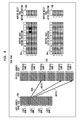
- FIG. 7 is a conceptual diagram illustrating how the final physical bank identifications are generated if there are no conflicts in any concurrent read and/or write operations, according to an embodiment of the invention.
- the diagram includes logical address space 700 , physical address space 702 , mapping table memory before operations are performed 704 , mapping table memory after operations are performed 706 , a select table before operations are performed 708 , and a select table after operations are performed 710 .
- the following read and write operations are received by the 1R2W SRAM concurrently:
- the physical bank identification is obtained from the mapping table memory 704 .
- the physical bank identification is stored at the intersection of a row number of the mapping table memory 704 , which is indicated by the address offset, and a column number of the mapping table memory 704 , which is indicated by the logical bank identification.
- the physical bank identification is found at the intersection of row 1 and column 1, which is 2 in mapping table memory 704 .
- the read operation is directed to physical memory bank 2 with an address offset of 0x01 or 1.
- the physical bank identification is obtained from the mapping table memory 704 .
- the physical bank identification is stored at the intersection of a row number of the mapping table memory 704 indicated by the address offset and a column number of the mapping table memory 704 indicated by the logical bank identification.
- the physical bank identification is found at the intersection of row 2 and column 1, which is 1 in mapping table memory 704 .
- the write port 0 operation is directed to physical memory bank 1 with an address offset of 0x10 or 2.
- the physical bank identification is obtained from the mapping table memory 704 .
- the physical bank identification is stored at the intersection of a row number of the mapping table memory 704 indicated by the address offset and a column number of the mapping table memory 704 indicated by the logical bank identification.
- the physical bank identification is found at the intersection of row 3 and column 1, which is 3 in mapping table memory 704 .
- the write port 0 operation is directed to physical memory bank 3 with an address offset of 0x11 or 3.
- mapping table controller Since the retrieved write and read physical bank identifications are different, no conflict is detected by the mapping table controller. Thus, the retrieved physical bank identification, which is 1 for write port 0, is used as the final write physical bank identification for write port 0, and 0x55 is written to bank 1 with an address offset of 2. Similarly, the retrieved physical bank identification, which is 3 for write port 1, is used as the final write physical bank identification for write port 1, and 0xaa is written to bank 3 with an address offset of 3. No mapping table memory or select table updates are required, and thus mapping tables 704 , 706 are the same and select tables 708 , 710 are the same.
- FIG. 8 is a conceptual diagram illustrating how final physical bank identifications are generated if there is a conflict concerning the read port and write port 0, according to an embodiment of the invention.
- the following read and write operations are received by the 1R2W memory concurrently:
- the physical bank identification is obtained from the mapping table memory 804 .
- the physical bank identification is stored at the intersection of a row number of the mapping table memory 804 indicated by the address offset, and a column number of the mapping table memory 804 indicated by the logical bank identification.
- the physical bank identification is found at the intersection of row 1 and column 1, which is 2 in mapping table memory 804 .
- the read operation is directed to physical bank 2 with an address offset of 0x01 or 1.
- the physical bank identification is obtained from mapping table memory 804 .
- the physical bank identification is stored at the intersection of a row number of the mapping table memory 804 indicated by the address offset and a column number of the mapping table memory 804 indicated by the logical bank identification. Thus, the physical bank identification is found at the intersection of row 2 and column 2, which is 2 in mapping table memory 804 .
- the physical bank identification is obtained from mapping table memory 804 .
- the physical bank identification is stored at the intersection of a row number of the mapping table memory 804 indicated by the address offset and a column number of the mapping table memory 804 indicated by the logical bank identification.
- the physical bank identification is found at the intersection of row 3 and column 1, which is 3 in mapping table memory 804 .
- mapping table memory 804 and mapping table memory 806 represent the mapping table memory before and after the operations are performed, respectively. At row 2 of the mapping table memory 804 , the physical bank identifications located at column 2 and column s0 are swapped due to redirection of the write port 0 data, as shown in mapping table memory 806 .
- the select table is also updated by writing a “0” into row (address offset) 2 of the select table 810 , which indicates that the mapping information at row (offset) 2 is located in table A of the mapping table memory after the operation is completed.
- entries in the mapping table 804 , 806 and select table 808 , 810 will change, and any entry in the select table may be “0” or “1”.
- the write port 1 operation has no conflict, and thus will not cause any mapping table memory or select table updates.
- FIG. 9 is a conceptual diagram illustrating how the final physical bank identifications are generated if there is a conflict between the read port, write port 0, and write port 1, according to an embodiment of the invention.
- read and write operations are received concurrently:
- the physical bank identification is obtained from mapping table memory 904 .
- the physical bank identification is stored at the intersection of a row number of the mapping table memory 904 indicated by the address offset, and a column number of the mapping table memory 904 indicated by the logical bank identification.
- the physical bank identification is found at the intersection of row 1 and column 1, which is 2 in mapping table memory 904 .
- the read operation is directed to physical bank 2 with an address offset of 0x01 or 1.
- the physical bank identification is obtained from mapping table memory 904 .
- the physical bank identification is stored at the intersection of a row number of the mapping table memory 904 indicated by the address offset, and a column number of the mapping table memory 904 indicated by the logical bank identification. Thus, the physical bank identification is found at the intersection of row 2 and column 1, which is 2 in mapping table memory 904 .
- the physical bank identification is obtained from mapping table memory 904 .
- the physical bank identification is stored at the intersection of a row number of the mapping table memory 904 indicated by the address offset and a column number of the mapping table memory 904 indicated by the logical bank identification.
- the physical bank identification is found at the intersection of row 3 and column 1, which is 2 in mapping table memory 904 .
- mapping table controller directs write port 0 and write port 1 operations to spare locations in the memory banks to avoid collision.
- the write port 0 operation is directed to a spare location in bank 4 and the write port 1 operation is directed to a spare location in bank 5.
- Mapping table memory 904 and mapping table memory 906 represent the mapping table memory before and after the operations are performed, respectively.
- the physical bank identifications located at column 1 and column s0 are swapped due to redirection of the write port 0 data.
- the mapping select table is also updated by writing a “0” into offset (row) 2 of the select table 910 , which indicates that the mapping information at offset (row) 2 is located in table A after the operation is performed.
- mapping tables 904 , 906 and select tables 908 , 910 will change, and any entry in the select table may be “0” or “1”.
- the mapping select table is also updated by writing a “1” into offset (row) 3 of the select table 910 , which indicates that the mapping information at offset (row) 3 is located in table B after the operation is performed. That is, the write port 1 operation is redirected due to the impending collision, and thus the physical bank identifications of the spare location and the bank originally intended for the write port 1 operation are swapped. Stated differently, the spare location will be mapped to a different physical bank. Accordingly, table B is updated, and the select table is updated by writing a “1” to the relevant entry to indicate that the new mapping information at offset 3 is now in table B, not table A.
- the read port operation and write port 0 operations are directed to the requested physical banks, and the write port 1 operation is directed to spare locations in any of the memory banks
- the memory includes sixteen entries, which are indexed from 0 to 15.
- the entire logical memory space is divisible into four equivalent logical memory banks, each of which accommodates four memory locations.
- FIG. 10 depicts an illustrative alternative embodiment of the 3R2W mapping table referred to in the examples discussed above, which could also be implemented using 1R2W cell or a register file, according to an embodiment of the invention.
- FIG. 11 conceptually illustrates memory organization in the embodiments disclosed herein.
- the memory location 1102 which is located at offset 1 of bank 2
- logical address 9 is mapped to physical address 1001 b
- the most significant two bits (10) represent the logical bank identification and the least significant two bits (01) represent the offset.
- two additional banks are used to support functionality of the 1R2W SRAM.
- spare entries 1110 are not fixed at any specific memory bank, but may be moved to any of the memory banks 1112 , 1114 , 1116 , 1118 , 1120 , 1122 in response to a memory access conflict, and thus spare entries can occur in any of the memory banks 1112 , 1114 , 1116 , 1118 , 1120 , 1122 .
- embodiments described herein support single-port read and multiple-port write functionality. Multiple-port write operations are supported by adding additional 1RW memory banks so that write data is redirected to the spare location in the memory banks in response to a conflict between operations requesting access to the same physical memory bank during the same memory cycle.
- the mapping table memory is updated after the write operation is redirected.
- the mapping table memory update reflects any changes in the mapping table memory so that a subsequent read operation is directed to the appropriate memory bank.
- static random access memory has been described in various embodiments of the invention, embodiments of the invention are not limited thereto. Any suitable form of memory is contemplated to be within the scope of embodiments of the invention including, but not limit to, Flash memory and erasable programmable read only memory.
- FIG. 10 An alternative embodiment of the 3R2W mapping table referred to in the examples discussed above, which could also be implemented using 1R2W cell or a register file, is shown in FIG. 10 , according to an embodiment of the invention.
- the mapping table 1000 in this embodiment is implemented using 1RW SRAM cells 1002 .
- Each of the 1R1W SRAM cells 414 - 424 shown in FIG. 4 is replaced with two 1RW SRAM cells 1002 of the same size and an additional multiplexer 1004 .
- the conflict resolution logic is configured, in the event there is a conflict between write port 0 and write port 1 operations without a conflict with the read operation: to direct the write port 0 operation to the originally intended physical bank and the write port 1 operation to the spare location in bank 0; to direct the write port 0 operation to the originally intended physical bank and the write port 1 operation to the spare location in bank 1; to direct the write port 1 operation to the originally intended physical bank and the write port 0 operation to the spare location in bank 0; or to direct the write port 1 operation to the originally intended physical bank and the write port 0 operation to the spare location in bank 0.
- At least a portion of the embodiments of the invention may be implemented in an integrated circuit.
- identical die are typically fabricated in a repeated pattern on a surface of a semiconductor wafer.
- Each die includes a device described herein, and may include other structures and/or circuits.
- the individual die are cut or diced from the wafer, then packaged as an integrated circuit.
- One skilled in the art would know how to dice wafers and package die to produce integrated circuits. Integrated circuits so manufactured are considered part of embodiments of the invention.
- An integrated circuit in accordance with embodiments of the invention can be employed in essentially any application and/or electronic system in which multi-port memories are utilized (e.g., two-port SRAM, two-port eDRAM, etc.).
- Suitable applications and systems for implementing techniques according to embodiments of the invention may include, but are not limited, to interface devices (e.g., interface networks, high-speed memory interfaces (e.g., DDR3, DDR4), etc.), personal computers, communication networks, electronic instruments (e.g., automated test equipment (ATE), measurement equipment, etc.), etc.
- ATE automated test equipment
- Systems incorporating such integrated circuits are considered part of embodiments of the invention. Given the teachings of embodiments of the invention provided herein, one of ordinary skill in the art will be able to contemplate other implementations and applications of the techniques of embodiments of the invention.
- one or more embodiments of the invention or elements thereof can be implemented in the form of an apparatus including a memory and at least one processor that is coupled with the memory and operative to perform, or facilitate the performance of, exemplary method steps for providing single-port read multiple-port write functionality in a memory.
- “facilitating” an action includes performing the action, making the action easier, helping to carry out the action, or causing the action to be performed.
- instructions executing on one processor might facilitate an action carried out by instructions executing on a remote processor, by sending appropriate data or commands to cause or aid the action to be performed.
- an actor facilitates an action by other than performing the action, the action is nevertheless performed by some entity or combination of entities.
- one or more embodiments of the invention or elements thereof can be implemented in the form of means for carrying out one or more of the methodologies described herein; the means can include (i) hardware module(s), (ii) software module(s) executing on one or more hardware processors, or (iii) a combination of hardware and software modules; any of (i)-(iii) implement the specific techniques set forth herein, and software modules relating to embodiments of the invention are stored in a tangible computer-readable recordable storage medium (or multiple such media). Appropriate interconnections via bus, network, and the like can also be included.
- Embodiments of the invention are referred to herein, individually and/or collectively, by the term “embodiment” merely for convenience and without intending to limit the scope of this application to any single embodiment or inventive concept if more than one is, in fact, shown.
- the term “embodiment” merely for convenience and without intending to limit the scope of this application to any single embodiment or inventive concept if more than one is, in fact, shown.
- this disclosure is intended to cover any and all adaptations or variations of various embodiments. Combinations of the above embodiments, and other embodiments not specifically described herein, will become apparent to those of skill in the art given the teachings herein.
Abstract
Description
| Table of Acronym Definitions |
| Acronym | Definition | ||
| 1R1W | Single-port read, single-port write | ||
| SRAM | Static random access memory | ||
| IC | Integrated circuit | ||
| 1RW | Single-port read or write (read/write) | ||
| 1RMW | Single-port read multiple-port write | ||
| MR1W | Multiple-port read single-port write | ||
| 1R2W | Single-port read dual-port write | ||
| 3R2W | Triple-port read double-port write | ||
| 2R1W | Double-port read single-port write | ||
| RE | Read enable | ||
| WE | Write enable | ||
| eDRAM | Embedded dynamic random access memory | ||
Claims (19)
Priority Applications (1)
| Application Number | Priority Date | Filing Date | Title |
|---|---|---|---|
| US13/725,028 US8923089B2 (en) | 2012-12-21 | 2012-12-21 | Single-port read multiple-port write storage device using single-port memory cells |
Applications Claiming Priority (1)
| Application Number | Priority Date | Filing Date | Title |
|---|---|---|---|
| US13/725,028 US8923089B2 (en) | 2012-12-21 | 2012-12-21 | Single-port read multiple-port write storage device using single-port memory cells |
Publications (2)
| Publication Number | Publication Date |
|---|---|
| US20140177324A1 US20140177324A1 (en) | 2014-06-26 |
| US8923089B2 true US8923089B2 (en) | 2014-12-30 |
Family
ID=50974487
Family Applications (1)
| Application Number | Title | Priority Date | Filing Date |
|---|---|---|---|
| US13/725,028 Expired - Fee Related US8923089B2 (en) | 2012-12-21 | 2012-12-21 | Single-port read multiple-port write storage device using single-port memory cells |
Country Status (1)
| Country | Link |
|---|---|
| US (1) | US8923089B2 (en) |
Families Citing this family (18)
| Publication number | Priority date | Publication date | Assignee | Title |
|---|---|---|---|---|
| US9256531B2 (en) * | 2012-06-19 | 2016-02-09 | Samsung Electronics Co., Ltd. | Memory system and SoC including linear addresss remapping logic |
| JP6070315B2 (en) * | 2013-03-18 | 2017-02-01 | 富士通株式会社 | Register file device and information processing device |
| US11099746B2 (en) * | 2015-04-29 | 2021-08-24 | Marvell Israel (M.I.S.L) Ltd. | Multi-bank memory with one read port and one or more write ports per cycle |
| US10089018B2 (en) * | 2015-05-07 | 2018-10-02 | Marvell Israel (M.I.S.L) Ltd. | Multi-bank memory with multiple read ports and multiple write ports per cycle |
| US10055365B2 (en) * | 2015-07-24 | 2018-08-21 | Mediatek Inc. | Shared buffer arbitration for packet-based switching |
| KR20170075359A (en) * | 2015-12-23 | 2017-07-03 | 에스케이하이닉스 주식회사 | Memory system and operation method of memory controller |
| US10089243B2 (en) * | 2016-02-25 | 2018-10-02 | SK Hynix Inc. | Memory controller and system including variable address mapping tables and a fixed address mapping table |
| CN106250321B (en) * | 2016-07-28 | 2019-03-01 | 盛科网络(苏州)有限公司 | The data processing method and data processing system of 2R1W memory |
| CN106297861B (en) * | 2016-07-28 | 2019-02-22 | 盛科网络(苏州)有限公司 | The data processing method and data processing system of expansible multiport memory |
| US10168938B2 (en) * | 2016-11-25 | 2019-01-01 | Hughes Network Systems, Llc | LDPC decoder design to significantly increase throughput in ASIC by utilizing pseudo two port memory structure |
| WO2020026155A1 (en) * | 2018-07-30 | 2020-02-06 | Marvell World Trade Ltd. | Patent application |
| CN113227984B (en) * | 2018-12-22 | 2023-12-15 | 华为技术有限公司 | Processing chip, method and related equipment |
| US11216212B2 (en) | 2019-03-19 | 2022-01-04 | International Business Machines Corporation | Minimizing conflicts in multiport banked memory arrays |
| US11538546B2 (en) * | 2019-12-16 | 2022-12-27 | Micron Technology, Inc. | Data compression for global column repair |
| CN113495676B (en) * | 2020-04-01 | 2023-09-29 | 长鑫存储技术有限公司 | Read-write method and memory device |
| CN113495674B (en) | 2020-04-01 | 2023-10-10 | 长鑫存储技术有限公司 | Read-write method and memory device |
| JP2023528933A (en) * | 2020-06-15 | 2023-07-06 | 日本電気株式会社 | Information processing device, image processing unit, method and program |
| CN112764687B (en) * | 2021-01-26 | 2023-02-28 | 山东云海国创云计算装备产业创新中心有限公司 | Data writing method and system, IC chip and electronic equipment |
Citations (13)
| Publication number | Priority date | Publication date | Assignee | Title |
|---|---|---|---|---|
| US5313611A (en) * | 1989-01-23 | 1994-05-17 | Eastman Kodak Company | Method and apparatus for maintaining a lookup table for storing function values |
| US5559450A (en) * | 1995-07-27 | 1996-09-24 | Lucent Technologies Inc. | Field programmable gate array with multi-port RAM |
| US6189073B1 (en) | 1995-11-17 | 2001-02-13 | Micron Technology, Inc. | Method of emulating a dual-port memory device using an internally cached static random access memory architecture |
| US20030097520A1 (en) * | 2001-11-16 | 2003-05-22 | Lai Chen Nan | Control device applicable to flash memory card and method for building partial lookup table |
| US6882562B2 (en) | 2001-11-01 | 2005-04-19 | Agilent Technologies, Inc. | Method and apparatus for providing pseudo 2-port RAM functionality using a 1-port memory cell |
| US20070183241A1 (en) | 2005-12-30 | 2007-08-09 | Stmicroelectronics Pvt. Ltd. | First-in first-out (FIFO) memory with multi-port functionality |
| US20070223017A1 (en) * | 2006-03-23 | 2007-09-27 | Fujitsu Limited | Image processing apparatus |
| US7333381B2 (en) | 2004-01-28 | 2008-02-19 | Marvel Semiconductor Israel Ltd. | Circuitry and methods for efficient FIFO memory |
| US7461191B2 (en) | 2004-08-31 | 2008-12-02 | Advanced Micro Devices, Inc. | Segmented on-chip memory and requester arbitration |
| US7533222B2 (en) | 2006-06-29 | 2009-05-12 | Mosys, Inc. | Dual-port SRAM memory using single-port memory cell |
| US7903497B2 (en) | 2007-10-24 | 2011-03-08 | Novelics, Llc | Multi-port SRAM implemented with single-port 6-transistor memory cells coupled to an input multiplexer and an output demultiplexer |
| US20120243285A1 (en) * | 2011-03-24 | 2012-09-27 | Easic Corporation | Multiple write during simultaneous memory access of a multi-port memory device |
| US20130346706A1 (en) * | 2011-11-07 | 2013-12-26 | Huawei Technologies Co., Ltd. | Data reading/writing method and memory device |
-
2012
- 2012-12-21 US US13/725,028 patent/US8923089B2/en not_active Expired - Fee Related
Patent Citations (13)
| Publication number | Priority date | Publication date | Assignee | Title |
|---|---|---|---|---|
| US5313611A (en) * | 1989-01-23 | 1994-05-17 | Eastman Kodak Company | Method and apparatus for maintaining a lookup table for storing function values |
| US5559450A (en) * | 1995-07-27 | 1996-09-24 | Lucent Technologies Inc. | Field programmable gate array with multi-port RAM |
| US6189073B1 (en) | 1995-11-17 | 2001-02-13 | Micron Technology, Inc. | Method of emulating a dual-port memory device using an internally cached static random access memory architecture |
| US6882562B2 (en) | 2001-11-01 | 2005-04-19 | Agilent Technologies, Inc. | Method and apparatus for providing pseudo 2-port RAM functionality using a 1-port memory cell |
| US20030097520A1 (en) * | 2001-11-16 | 2003-05-22 | Lai Chen Nan | Control device applicable to flash memory card and method for building partial lookup table |
| US7333381B2 (en) | 2004-01-28 | 2008-02-19 | Marvel Semiconductor Israel Ltd. | Circuitry and methods for efficient FIFO memory |
| US7461191B2 (en) | 2004-08-31 | 2008-12-02 | Advanced Micro Devices, Inc. | Segmented on-chip memory and requester arbitration |
| US20070183241A1 (en) | 2005-12-30 | 2007-08-09 | Stmicroelectronics Pvt. Ltd. | First-in first-out (FIFO) memory with multi-port functionality |
| US20070223017A1 (en) * | 2006-03-23 | 2007-09-27 | Fujitsu Limited | Image processing apparatus |
| US7533222B2 (en) | 2006-06-29 | 2009-05-12 | Mosys, Inc. | Dual-port SRAM memory using single-port memory cell |
| US7903497B2 (en) | 2007-10-24 | 2011-03-08 | Novelics, Llc | Multi-port SRAM implemented with single-port 6-transistor memory cells coupled to an input multiplexer and an output demultiplexer |
| US20120243285A1 (en) * | 2011-03-24 | 2012-09-27 | Easic Corporation | Multiple write during simultaneous memory access of a multi-port memory device |
| US20130346706A1 (en) * | 2011-11-07 | 2013-12-26 | Huawei Technologies Co., Ltd. | Data reading/writing method and memory device |
Non-Patent Citations (1)
| Title |
|---|
| Ronald L. Rivest and Lance A. Glasser, "A Fast Multiport Memory Based on Single-Port Memory Cells," Jul. 1991, pp. 1-12, MIT Laboratory for Computer Science, Cambridge, MA. |
Also Published As
| Publication number | Publication date |
|---|---|
| US20140177324A1 (en) | 2014-06-26 |
Similar Documents
| Publication | Publication Date | Title |
|---|---|---|
| US8923089B2 (en) | Single-port read multiple-port write storage device using single-port memory cells | |
| US8374050B2 (en) | Multi-port memory using single-port memory cells | |
| US5835941A (en) | Internally cached static random access memory architecture | |
| KR100244841B1 (en) | High-speed, multiple-port, interleaved cache with arbitration of multiple access addresses | |
| US8724423B1 (en) | Synchronous two-port read, two-port write memory emulator | |
| US9030894B2 (en) | Hierarchical multi-bank multi-port memory organization | |
| US10818325B2 (en) | Data processing method and data processing system for scalable multi-port memory | |
| US20140047197A1 (en) | Multiport memory emulation using single-port memory devices | |
| US8305834B2 (en) | Semiconductor memory with memory cell portions having different access speeds | |
| US20190332313A1 (en) | Data buffer processing method and data buffer processing system for 4r4w fully-shared packet | |
| CN101169772A (en) | Method and apparatus for transmitting command and address signals | |
| JP5599969B2 (en) | Multi-port memory and computer system including the multi-port memory | |
| EP3038109B1 (en) | Pseudo dual port memory using a dual port cell and a single port cell with associated valid data bits and related methods | |
| US7093047B2 (en) | Integrated circuit memory devices having clock signal arbitration circuits therein and methods of performing clock signal arbitration | |
| CN106250321B (en) | The data processing method and data processing system of 2R1W memory | |
| US10580481B1 (en) | Methods, circuits, systems, and articles of manufacture for state machine interconnect architecture using embedded DRAM | |
| US9003121B2 (en) | Multi-ported memory with multiple access support | |
| WO2013097228A1 (en) | Multi-granularity parallel storage system | |
| US20060155940A1 (en) | Multi-queue FIFO memory systems that utilize read chip select and device identification codes to control one-at-a-time bus access between selected FIFO memory chips | |
| US20130332665A1 (en) | Memory with bank-conflict-resolution (bcr) module including cache | |
| US8671262B2 (en) | Single-port memory with addresses having a first portion identifying a first memory block and a second portion identifying a same rank in first, second, third, and fourth memory blocks | |
| TW202230352A (en) | Memory circuit architecture | |
| KR20210091404A (en) | Memory device and operating method of memory device | |
| JP2005122852A (en) | Semiconductor memory device | |
| US20230359573A1 (en) | Field programmable gate array (fpga) for implementing data transmission by using built-in edge module |
Legal Events
| Date | Code | Title | Description |
|---|---|---|---|
| AS | Assignment |
Owner name: LSI CORPORATION, CALIFORNIA Free format text: ASSIGNMENT OF ASSIGNORS INTEREST;ASSIGNORS:LIU, SHENG;ZHOU, TING;SIGNING DATES FROM 20121214 TO 20121217;REEL/FRAME:029521/0285 |
|
| AS | Assignment |
Owner name: DEUTSCHE BANK AG NEW YORK BRANCH, AS COLLATERAL AG Free format text: PATENT SECURITY AGREEMENT;ASSIGNORS:LSI CORPORATION;AGERE SYSTEMS LLC;REEL/FRAME:032856/0031 Effective date: 20140506 |
|
| AS | Assignment |
Owner name: AVAGO TECHNOLOGIES GENERAL IP (SINGAPORE) PTE. LTD Free format text: ASSIGNMENT OF ASSIGNORS INTEREST;ASSIGNOR:LSI CORPORATION;REEL/FRAME:035390/0388 Effective date: 20140814 |
|
| AS | Assignment |
Owner name: LSI CORPORATION, CALIFORNIA Free format text: TERMINATION AND RELEASE OF SECURITY INTEREST IN PATENT RIGHTS (RELEASES RF 032856-0031);ASSIGNOR:DEUTSCHE BANK AG NEW YORK BRANCH, AS COLLATERAL AGENT;REEL/FRAME:037684/0039 Effective date: 20160201 Owner name: AGERE SYSTEMS LLC, PENNSYLVANIA Free format text: TERMINATION AND RELEASE OF SECURITY INTEREST IN PATENT RIGHTS (RELEASES RF 032856-0031);ASSIGNOR:DEUTSCHE BANK AG NEW YORK BRANCH, AS COLLATERAL AGENT;REEL/FRAME:037684/0039 Effective date: 20160201 |
|
| AS | Assignment |
Owner name: BANK OF AMERICA, N.A., AS COLLATERAL AGENT, NORTH CAROLINA Free format text: PATENT SECURITY AGREEMENT;ASSIGNOR:AVAGO TECHNOLOGIES GENERAL IP (SINGAPORE) PTE. LTD.;REEL/FRAME:037808/0001 Effective date: 20160201 Owner name: BANK OF AMERICA, N.A., AS COLLATERAL AGENT, NORTH Free format text: PATENT SECURITY AGREEMENT;ASSIGNOR:AVAGO TECHNOLOGIES GENERAL IP (SINGAPORE) PTE. LTD.;REEL/FRAME:037808/0001 Effective date: 20160201 |
|
| AS | Assignment |
Owner name: AVAGO TECHNOLOGIES GENERAL IP (SINGAPORE) PTE. LTD., SINGAPORE Free format text: TERMINATION AND RELEASE OF SECURITY INTEREST IN PATENTS;ASSIGNOR:BANK OF AMERICA, N.A., AS COLLATERAL AGENT;REEL/FRAME:041710/0001 Effective date: 20170119 Owner name: AVAGO TECHNOLOGIES GENERAL IP (SINGAPORE) PTE. LTD Free format text: TERMINATION AND RELEASE OF SECURITY INTEREST IN PATENTS;ASSIGNOR:BANK OF AMERICA, N.A., AS COLLATERAL AGENT;REEL/FRAME:041710/0001 Effective date: 20170119 |
|
| FEPP | Fee payment procedure |
Free format text: MAINTENANCE FEE REMINDER MAILED (ORIGINAL EVENT CODE: REM.); ENTITY STATUS OF PATENT OWNER: LARGE ENTITY |
|
| AS | Assignment |
Owner name: AVAGO TECHNOLOGIES INTERNATIONAL SALES PTE. LIMITE Free format text: MERGER;ASSIGNOR:AVAGO TECHNOLOGIES GENERAL IP (SINGAPORE) PTE. LTD.;REEL/FRAME:047642/0417 Effective date: 20180509 |
|
| LAPS | Lapse for failure to pay maintenance fees |
Free format text: PATENT EXPIRED FOR FAILURE TO PAY MAINTENANCE FEES (ORIGINAL EVENT CODE: EXP.); ENTITY STATUS OF PATENT OWNER: LARGE ENTITY |
|
| STCH | Information on status: patent discontinuation |
Free format text: PATENT EXPIRED DUE TO NONPAYMENT OF MAINTENANCE FEES UNDER 37 CFR 1.362 |
|
| FP | Expired due to failure to pay maintenance fee |
Effective date: 20181230 |
|
| AS | Assignment |
Owner name: AVAGO TECHNOLOGIES INTERNATIONAL SALES PTE. LIMITE Free format text: CORRECTIVE ASSIGNMENT TO CORRECT THE EXECUTION DATE OF THE MERGER PREVIOUSLY RECORDED ON REEL 047642 FRAME 0417. ASSIGNOR(S) HEREBY CONFIRMS THE ASSIGNMENT,;ASSIGNOR:AVAGO TECHNOLOGIES GENERAL IP (SINGAPORE) PTE. LTD.;REEL/FRAME:048521/0395 Effective date: 20180905 |