US8924636B2 - Management information generating method, logical block constructing method, and semiconductor memory device - Google Patents
Management information generating method, logical block constructing method, and semiconductor memory device Download PDFInfo
- Publication number
- US8924636B2 US8924636B2 US13/609,991 US201213609991A US8924636B2 US 8924636 B2 US8924636 B2 US 8924636B2 US 201213609991 A US201213609991 A US 201213609991A US 8924636 B2 US8924636 B2 US 8924636B2
- Authority
- US
- United States
- Prior art keywords
- block
- physical
- blocks
- logical
- logical block
- Prior art date
- Legal status (The legal status is an assumption and is not a legal conclusion. Google has not performed a legal analysis and makes no representation as to the accuracy of the status listed.)
- Active, expires
Links
Images


Classifications
-
- G—PHYSICS
- G06—COMPUTING; CALCULATING OR COUNTING
- G06F—ELECTRIC DIGITAL DATA PROCESSING
- G06F12/00—Accessing, addressing or allocating within memory systems or architectures
- G06F12/02—Addressing or allocation; Relocation
- G06F12/0223—User address space allocation, e.g. contiguous or non contiguous base addressing
- G06F12/023—Free address space management
- G06F12/0238—Memory management in non-volatile memory, e.g. resistive RAM or ferroelectric memory
- G06F12/0246—Memory management in non-volatile memory, e.g. resistive RAM or ferroelectric memory in block erasable memory, e.g. flash memory
-
- G—PHYSICS
- G06—COMPUTING; CALCULATING OR COUNTING
- G06F—ELECTRIC DIGITAL DATA PROCESSING
- G06F12/00—Accessing, addressing or allocating within memory systems or architectures
- G06F12/02—Addressing or allocation; Relocation
- G06F12/08—Addressing or allocation; Relocation in hierarchically structured memory systems, e.g. virtual memory systems
- G06F12/10—Address translation
- G06F12/109—Address translation for multiple virtual address spaces, e.g. segmentation
-
- G—PHYSICS
- G06—COMPUTING; CALCULATING OR COUNTING
- G06F—ELECTRIC DIGITAL DATA PROCESSING
- G06F12/00—Accessing, addressing or allocating within memory systems or architectures
- G06F12/02—Addressing or allocation; Relocation
- G06F12/08—Addressing or allocation; Relocation in hierarchically structured memory systems, e.g. virtual memory systems
- G06F12/10—Address translation
- G06F12/1009—Address translation using page tables, e.g. page table structures
-
- G—PHYSICS
- G06—COMPUTING; CALCULATING OR COUNTING
- G06F—ELECTRIC DIGITAL DATA PROCESSING
- G06F12/00—Accessing, addressing or allocating within memory systems or architectures
- G06F12/02—Addressing or allocation; Relocation
- G06F12/08—Addressing or allocation; Relocation in hierarchically structured memory systems, e.g. virtual memory systems
- G06F12/10—Address translation
- G06F12/1027—Address translation using associative or pseudo-associative address translation means, e.g. translation look-aside buffer [TLB]
- G06F12/1036—Address translation using associative or pseudo-associative address translation means, e.g. translation look-aside buffer [TLB] for multiple virtual address spaces, e.g. segmentation
-
- G—PHYSICS
- G06—COMPUTING; CALCULATING OR COUNTING
- G06F—ELECTRIC DIGITAL DATA PROCESSING
- G06F2212/00—Indexing scheme relating to accessing, addressing or allocation within memory systems or architectures
- G06F2212/10—Providing a specific technical effect
- G06F2212/1032—Reliability improvement, data loss prevention, degraded operation etc
-
- G—PHYSICS
- G06—COMPUTING; CALCULATING OR COUNTING
- G06F—ELECTRIC DIGITAL DATA PROCESSING
- G06F2212/00—Indexing scheme relating to accessing, addressing or allocation within memory systems or architectures
- G06F2212/72—Details relating to flash memory management
- G06F2212/7201—Logical to physical mapping or translation of blocks or pages
-
- G—PHYSICS
- G11—INFORMATION STORAGE
- G11C—STATIC STORES
- G11C16/00—Erasable programmable read-only memories
- G11C16/02—Erasable programmable read-only memories electrically programmable
- G11C16/06—Auxiliary circuits, e.g. for writing into memory
- G11C16/34—Determination of programming status, e.g. threshold voltage, overprogramming or underprogramming, retention
- G11C16/349—Arrangements for evaluating degradation, retention or wearout, e.g. by counting erase cycles
Definitions
- Embodiments described herein relate generally to a management information generating method, a logical block constructing method, and a semiconductor memory device.
- NAND flash memory that is a nonvolatile semiconductor memory device
- SSD Solid State Drive
- a management table in a volatile memory is directly stored in a NAND flash memory that is a nonvolatile memory.
- a volatile memory of a large memory size is needed.
- a long time is required for reading the management table from the NAND flash memory to the volatile memory. Therefore, it is desirable to reduce the size of the management table.
- a logical block as a virtual block, in which a plurality of physical blocks as a unit for erasing in a flash memory is combined, is introduced, and erasing, writing, and reading are each performed in parallel in units of logical blocks, thereby improving the write amplification factor and achieving speed-up by the parallel processing.
- a bad block which cannot be used as a storage area, is already included in the manufacturing stage in some cases. Moreover, when an SSD is used, a bad block is generated in some cases.
- the former bad block is referred to as a congenital bad block and the latter bad block is referred to as an acquired bad block.
- a logical block is in some cases composed of physical blocks excluding such a bad block.
- data stored in a flash memory includes user data that a user stores therein and system data as management information used in the SSD.
- system data as management information used in the SSD.
- FIG. 1 is a block diagram illustrating a configuration example of an SSD according to a first embodiment
- FIG. 2 is a diagram for explaining address translation performed in the SSD
- FIG. 3A is a diagram illustrating a configuration example of a block address BA) translation table according to the first embodiment
- FIG. 3B is a diagram illustrating a configuration example of a validity management table according to the first embodiment
- FIG. 4 is a flowchart illustrating a data read processing procedure from a NAND memory
- FIG. 5 is a flowchart illustrating a construction processing procedure of a BA translation table according to a second embodiment
- FIG. 6 is a diagram for explaining a first half of construction processing of the BA translation table according to the second embodiment
- FIG. 7 is a diagram for explaining a last half of construction processing of the BA translation table according to the second embodiment.
- FIG. 8A is a diagram illustrating a configuration example of the BA translation table according to the second embodiment and FIG. 8B is a diagram illustrating a configuration example of a validity management table;
- FIG. 9 is a block diagram illustrating an internal configuration example of an SSD according to a third embodiment.
- FIG. 10 is a diagram illustrating an internal configuration example of a NAND according to the third embodiment.
- FIG. 11 is a diagram illustrating the types of a logical block
- FIG. 12 is a diagram illustrating an address translation table according to the third embodiment.
- FIG. 13 is a diagram illustrating a logical block management table
- FIG. 14 is a diagram illustrating a bad block table
- FIG. 15 is a flowchart illustrating a construction procedure of a logical block at the initial start-up
- FIG. 16 is a diagram conceptually illustrating reconstruction of a logical block
- FIG. 17 is a diagram illustrating a life cycle of a logical block
- FIG. 18 is a flowchart illustrating a detailed procedure of determination processing
- FIG. 19 is a flowchart illustrating a reconstruction procedure of a logical block when an SSD is used
- FIG. 20 is a diagram conceptually illustrating an example of reconstruction of a logical block when an SSD is used
- FIG. 21 is a block diagram illustrating an internal configuration example of an SSD according to a fourth embodiment
- FIG. 22 is a diagram illustrating an internal configuration example of a NAND according to the fourth embodiment.
- FIG. 23 is a diagram illustrating a system block table
- FIG. 24 is a diagram illustrating a user block table
- FIG. 25 is a flowchart illustrating a construction procedure of a logical block
- FIG. 26 is a diagram conceptually illustrating selection processing of a system block in the fourth embodiment.
- FIG. 27 is a flowchart illustrating a construction procedure of a system logical block
- FIG. 28 is a diagram conceptually illustrating selection processing of a system block in a fifth embodiment
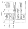
- FIG. 29 is a block diagram illustrating an internal configuration example of an SSD according to a sixth embodiment.
- FIG. 30 is a diagram illustrating an internal configuration example of a NAND according to the sixth embodiment.
- FIG. 31 is a diagram illustrating an address translation table according to the sixth embodiment.
- FIG. 32 is a diagram illustrating a logical block management table
- FIG. 33 is a diagram conceptually illustrating block management
- FIG. 34 is a diagram illustrating a breakdown of a total capacity of a NAND
- FIG. 35 is a flowchart illustrating a procedure of determining block depletion
- FIG. 36 is a flowchart illustrating a procedure of determining block depletion
- FIG. 37 is a perspective view illustrating an appearance of a personal computer according to the sixth embodiment.
- FIG. 38 is a diagram illustrating a system configuration example of the personal computer according to the sixth embodiment.
- a physical block address group is generated by extracting a first predetermined number of physical block addresses in a nonvolatile memory arranged in a semiconductor memory device used as an external memory device of a computer system at a time in ascending order of an address value. Moreover, when a physical block address of a bad block is included in the physical block address group, a next physical block address group is generated by setting a physical block address of a first good block after the bad block as a top physical block address of the next physical block address group. Then, all physical block addresses from a first bad block are set to the 1st bad block in each of physical block address groups.
- a physical block address group set is generated by extracting a second predetermined number of physical block address groups at a time from all of the physical block address groups in descending order of the number of good blocks.
- the 2nd bad block is set to each physical block address group so that the number of continuous bad blocks and the number of continuous good blocks from a top in each physical block address group have the same value as a physical block address group in which the number of good blocks is the smallest in a physical block address group set, in each of generated physical block address group sets.
- An address management table is generated in which a logical block address group, which is a plurality of continuous logical block addresses set by using a logical block address in the nonvolatile memory corresponding to a logical address specified from a host device, and a physical block address group set are associated with each other.
- a management information generating method, a logical block constructing method, and a semiconductor memory device according embodiments will be explained below in detail with reference to the accompanying drawings.
- the present invention is not limited to these embodiments.
- FIG. 1 is a block diagram illustrating a configuration example of an SSD according to the first embodiment.
- An SSD (Solid State Drive) 1 A that is a semiconductor memory device (memory system) is an external memory device used in a computer system and includes a RAM (Random Access Memory) 2 A, a NAND memory 4 A (nonvolatile memory) that actually stores data, and a controller 3 A.
- RAM Random Access Memory
- NAND memory 4 A nonvolatile memory
- the RAM 2 A is connected to a host device 10 A, the controller 3 A, and the NAND memory 4 A. Moreover, the NAND memory 4 A is connected to the controller 3 A and the RAM 2 A. The controller 3 A is connected to the host device 10 A, the RAM 2 A, and the NAND memory 4 A.
- the RAM 2 A is a memory, such as an SRAM (Static Random Access Memory), a DRAM (Dynamic Random Access Memory), and an FERAM (Ferroelectric Random Access Memory).
- the RAM 2 A temporarily stores data sent from the host device 10 A and sends the stored data to the NAND memory 4 A. Moreover, when data for which a read request is issued from the host device 10 A is read from the NAND memory 4 A, the RAM 2 A temporarily stores the read data. The data that is read from the NAND memory 4 A and is temporarily stored in the RAM 2 A is sent to the host device 10 A.
- the RAM 2 A stores a host address translation table 21 A, a read/write buffer 22 A, a BA (block address) translation table 23 A and a validity management table 24 A that are management tables, and the like.
- the host address translation table 21 A is a translation table that indicates the correspondence relationship between a logical address provided from the host device 10 A and a logical block address in the NAND memory 4 A.
- a logical block in the NAND memory 4 A is one unit for erasing that is set in the SSD 1 A and is associated with one or more physical blocks.
- the BA translation table 23 A is a translation table (address management table) that indicates the correspondence relationship between a logical block address in the NAND memory 4 A and a physical block address (storage location) in the NAND memory 4 A and is used for address management (read/write control).
- a physical block is the minimum unit that is erasable independently in the NAND memory 4 A and is composed of a plurality of physical pages.
- a logical block address is referred to as a logical BA and a physical block address is referred to as a physical BA.
- the BA translation table 23 A in the present embodiment logical BAs of continuous address numbers are grouped. Moreover, physical BAs of continuous address numbers are grouped. Then, the grouped logical BAs and the grouped physical BAs are associated with each other.
- the validity management table 24 A is a table that indicates the validity of a logical BA, the number of times erasing is performed on a logical BA, and the like for each logical BA.
- the host address translation table 21 A, the BA translation table 23 A, and the validity management table 24 A are loaded from the NAND memory 4 A into the RAM 2 A at a predetermined timing, for example, when the SSD 1 A is activated.
- the host address translation table 21 A loaded in the RAM 2 A is updated.
- the BA translation table 23 A and the validity management table 24 A are constructed, for example, when the SSD 1 A is used for the first time. Moreover, when the validity of a logical BA, the number of times rewriting is performed on a logical BA, or the like is updated, the validity management table 24 A loaded in the RAM 2 A is updated.
- the read/write buffer 22 A is a buffer memory used when data transfer is performed between the NAND memory 4 A and the host device 10 A. Data read from the NAND memory 4 A is buffered in the read/write buffer 22 A and is sent to the host device 10 A. Moreover, data for which a write request is issued from the host device 10 A is buffered in the read/write buffer 22 A and is written in the NAND memory 4 A.
- the controller 3 A loads a table group (the host address translation table 21 A, the BA translation table 23 A, and the validity management table 24 A) stored in the NAND memory 4 A into the RAM 2 A at a predetermined timing (for example, at the time of activation) and causes the table group in the RAM 2 A to be stored in the NAND memory 4 A at a predetermined timing. Moreover, the controller 3 A performs data transfer between the host device 10 A and the NAND memory 4 A via the RAM 2 A.
- a table group the host address translation table 21 A, the BA translation table 23 A, and the validity management table 24 A
- the controller 3 A performs read/write control of data on the NAND memory 4 A by controlling the RAM 2 A and the NAND memory 4 A by using the BA translation table 23 A and the validity management table 24 A.
- the controller 3 A includes a table constructing unit (Generator) 31 A, a write control unit 32 A, a read control unit 33 A, a host address translation unit 34 A, and a block address translation unit 35 A.
- the table constructing unit 31 A constructs the BA translation table 23 A and the validity management table 24 A by using the continuity of the address number of a logical BA or a physical BA.
- the table constructing unit 31 A may construct the BA translation table 23 A and the validity management table 24 A at any time. Moreover, the table constructing unit 31 A may reconstruct the BA translation table 23 A and the validity management table 24 A as needed.
- the write control unit 32 A writes data in the NAND memory 4 A by using the host address translation table 21 A, the BA translation table 23 A, and the validity management table 24 A in the RAM 2 A.
- the read control unit 33 A reads data from the NAND memory 4 A by using the host address translation table 21 A, the BA translation table 23 A, and the validity management table 24 A in the RAM 2 A.
- the write control unit 32 A and the read control unit 33 A perform data management in the RAM 2 A and the NAND memory 4 A on the basis of the table group while updating the table group in the RAM 2 A and the NAND memory 4 A.
- the host address translation unit 34 A translates a logical address into a logical BA by using the host address translation table 21 A. Moreover, the host address translation unit 34 A translates a logical BA into a logical address by using the host address translation table 21 A.
- the block address translation unit 35 A translates a logical BA into a physical BA that is a storage location in the NAND memory 4 A by using the BA translation table 23 A and the validity management table 24 A. Moreover, the block address translation unit 35 A translates a physical BA into a logical BA by using the BA translation table 23 A and the validity management table 24 A.
- the write control unit 32 A selects an unused valid logical block (writable logical block) by referring to the validity management table 24 A. Then, the write control unit 32 A writes data specified by a logical address in the selected logical block. Furthermore, the write control unit 32 A registers the correspondence relationship between the logical BA of the selected logical block and the logical address in the host address translation table 21 A.
- the read control unit 33 A sends a data translation instruction to the host address translation unit 34 A and the block address translation unit 35 A. Consequently, the host address translation unit 34 A translates a logical address into a logical BA by using the host address translation table 21 A.
- the SSD 1 A receives a read/write instruction from the host device 10 A via a not-shown interface.
- the interface between the host device 10 A and the SSD 1 A for example, conforms to the SATA (Serial ATA) standard, however, it is not limited to this.
- the NAND memory 4 A is a nonvolatile semiconductor memory, such as a NAND flash memory.
- the NAND memory 4 A includes a memory cell array in which a plurality of nonvolatile memory cells is arranged in a matrix manner and a peripheral circuit for controlling write, read, and erase operations to the memory cell array.
- the memory cell array is configured by arranging a plurality of blocks such that one block is the minimum unit for data erasing.
- Each block is configured by arranging a plurality of pages such that one page is the minimum unit for data writing and data reading.
- Each memory cell may be configured to store 1 bit or may be configured to store 2 or more bits.
- rewriting to the same page in a block is not allowed until data in the entire block including the page is once erased.
- the data written from the host device 10 A to the SSD 1 A is stored in the NAND memory 4 A in predetermined management units.
- Continuous addresses in a logical BA space are set as one unit for logical-physical translation (translation from a logical BA to a physical BA) and the continuous addresses are collectively assigned to a physical area in the NAND memory 4 A.
- sectors of continuous logical BAs are sequentially arranged.
- the size of the management unit is arbitrary, however, for example, the size of the management unit can be made the same as the page size or the block size in the NAND memory 4 A, the cluster size in a file system used in the host device 10 A, or the like.
- the cluster size is equal or larger than the sector size and is equal to or smaller than the block size.
- a logical BA in the NAND memory 4 A to which data written from the host device 10 A is written dynamically changes, and the correspondence relationship thereof is managed by the host address translation table 21 A.
- a logical address for example, an LBA (Logical Block Addressing) in which serial numbers starting from zero are attached to a logical capacity in sector units is used.
- a logical address specified by the host device 10 A in a write request is the size of a sector unit, however, in the SSD 1 A, logical addresses are made to match the size of the management unit (for example, cluster size). Then, sectors corresponding to continuous LBAs in the management unit are collectively stored in an area in the management unit in the NAND memory 4 A. For example, when the size of the management unit is equal to the cluster size, a plurality of sectors corresponding to LBAs that are made to match the cluster size is written in an area of the cluster size of the NAND memory 4 A.
- FIG. 2 is a diagram for explaining address translation performed in the SSD.
- the host address translation table 21 A is a table that indicates a logical BA to which data specified by a logical address is written.
- the BA translation table 23 A is a table that indicates a physical BA in the NAND memory 4 A to which data indicated by a logical BA is written.
- a logical address 41 A is specified from the host device 10 A.
- the write control unit 32 A selects an unused valid logical block by referring to the validity management table 24 A. Then, the write control unit 32 A writes the data specified by the logical address in the selected logical block. Furthermore, the write control unit 32 A registers the correspondence relationship between the logical BA of the selected logical block and the logical address in the host address translation table 21 A. Furthermore, the block address translation unit 35 A translates a logical BA 42 A into a physical BA 43 A by using the BA translation table 23 A. Then, the write control unit 32 A sends a write command including the physical BA 43 A to the NAND memory 4 A. Consequently, data is written in the physical BA 43 A corresponding to the logical address 41 A.
- the logical address 41 A is specified from the host device 10 A.
- the host address translation unit 34 A translates the logical address 41 A into the logical BA 42 A by using the host address translation table 21 A.
- the block address translation unit 35 A translates the logical BA 42 A into the physical BA 43 A by using the BA translation table 23 A.
- the read control unit 33 A sends a read command including the physical BA 43 A to the NAND memory 4 A. Consequently, data is read from the physical BA 43 A corresponding to the logical address 41 A.
- FIG. 3A is a diagram illustrating a configuration example of the BA translation table according to the first embodiment
- FIG. 3B is a diagram illustrating a configuration example of the validity management table according to the first embodiment.
- logical BAs of continuous addresses and physical BAs of continuous addresses are associated with each other.
- logical BAs for continuous 16 blocks and physical BAs for continuous 16 blocks are associated with each other.
- the table constructing unit 31 A sets the logical BAs “ 00 ” to “ 15 ” for 16 blocks as one logical BA group.
- a plurality of logical BAs is set in one entry in the BA translation table 23 A.
- the group of the logical BAs “ 00 ” to “ 15 ” is indicated as a “logical BA 00 / 15 ”.
- the table constructing unit 31 A associates a set of physical BAs for 64 slots (physical BA group set) corresponding to the logical BAs “ 00 ” to “ 15 ” with the logical BAs “ 00 ” to “ 15 ”.
- Each physical BA group in a physical BA group set includes physical BAs for 16 blocks. Therefore, the table constructing unit 31 A, for example, sets physical BAs for 16 blocks as one physical BA group.
- the table constructing unit 31 A sets the physical BAs “x+0” to “x+15” for 16 blocks as one physical BA group and sets the physical BAs “v+0” to “v+15” for 16 blocks as one physical BA group.
- the table constructing unit 31 A assigns the physical BAs “x+0” to “x+15” to a physical BA group corresponding to the Slot “ 00 ” of the logical BAs “ 00 ” to “ 15 ”. Moreover, the table constructing unit 31 A assigns the physical BAs “v+0” to “v+15” to a physical BA group corresponding to the Slot “ 63 ” of the logical BAs “ 00 ” to “ 15 ”.
- the BA translation table 23 A for example, top addresses of the physical BAs “x+0” to “x+15”, the physical BAs “v+0” to “v+15”, and the like are registered.
- the physical BA group including the physical BAs “x+0” to “x+15” is indicated as a physical BA “x”.
- the physical BA group including the physical BAs “v+0” to “v+15” is indicated as a physical BA “v”.
- the table constructing unit 31 A sets logical BAs “N” to “N+15” (N is a multiple of 16) for 16 blocks as one logical BA group. Then, the table constructing unit 31 A registers physical BAs for 16 blocks as one physical BA group in each slot in the BA translation table 23 A. In this manner, the table constructing unit 31 A associates a physical BA group in each slot and a logical BA group with each other and registers it in the BA translation table 23 A.
- indexes such as the logical BAs “ 00 ” to “ 15 ” and the Slot “ 00 ”, are illustrated, however, the indexes may be omitted.
- a physical BA is read from the BA translation table 23 A on the premise that each logical BA group includes logical BAs for 16 blocks and the number of slots in each logical BA group is 64.
- a bad block which cannot be used as a storage area due to a large number of errors or the like, is included.
- a physical block becomes a bad block in some cases due to an erase error or a program error (write error).
- the validity management table 24 A illustrated in FIG. 3B is a table that manages the validity of each logical block.
- a logical BA of each logical block is associated with information (validity information) indicating the validity.
- a logical block in which the information indicating the validity is “valid” is a normal logical block (good block) (GB) and a logical block in which the information indicating the validity is “invalid” is a bad block.
- the logical BA “ 01 ” corresponding to the physical BA “v+1” is registered in the validity management table 24 A as “invalid”.
- the validity management table 24 A the number of times erasing is performed on each logical BA group or the like may be registered.
- FIG. 4 is a flowchart illustrating the data read processing procedure from the NAND memory.
- the host device 10 A sends a read command and the logical address 41 A that is a target for reading data to the controller 3 A of the SSD 1 A.
- the host address translation unit 34 A of the controller 3 A translates the logical address 41 A into the logical BA 42 A by using the host address translation table 21 A (Step S 10 A). At this time, the host address translation unit 34 A translates the logical address 41 A into the logical BA 42 A and an offset in the logical block.
- the value of the offset is a value used when the position of a slot is calculated and the unit of the offset is equal in size to the data management unit in the SSD 1 A.
- the host address translation unit 34 A calculates a Slot position C (C is any of 00 to 63 ) in advance by using the value of the offset.
- the block address translation unit 35 A translates the logical BA 42 A into the physical BA 43 A by using the BA translation table 23 A. Specifically, the block address translation unit 35 A calculates a quotient “A” and a remainder “B” obtained by dividing the logical BA by 16 (Step S 20 A). Then, the block address translation unit 35 A sets an (A+1)th stage of the BA translation table 23 A to a read target position of a physical BA. The block address translation unit 35 A extracts (reads) the physical BA at the Slot position C in the (A+1)th stage from the BA translation table 23 A (Step S 30 A). The block address translation unit 35 A calculates a value obtained by adding the “B” to the extracted physical BA as the physical BA 43 A that is a target for reading (Step S 40 A).
- the physical BA 43 A calculated by the block address translation unit 35 A becomes a physical BA corresponding to the logical address 41 A sent from the host device 10 A.
- the read control unit 33 A sends a read command including the physical BA 43 A to the NAND memory 4 A. Consequently, data in the physical BA 43 A corresponding to the logical address 41 A is read.
- a logical BA group and a physical BA group are each composed of a group of 16 block addresses, however, it is sufficient that a logical BA group and a physical BA group are each composed of a group of two or more block addresses.
- the number of slots allocated to a logical BA group may be less than 64 or equal to or more than 65.
- logical BAs of continuous addresses and physical BAs of continuous addresses are associated with each other in the BA translation table 23 A, therefore, the BA translation table 23 A can be compressed efficiently.
- the memory capacity of the RAM 2 A needed for the SSD 1 A can be reduced.
- the size of the BA translation table 23 A stored in the NAND memory 4 A and the RAM 2 A becomes small, the life of the SSD 1 A can be extended. Moreover, because the size of the BA translation table 23 A stored in the NAND memory 4 A becomes small, the time required for writing and reading the BA translation table 23 A to and from the NAND memory 4 A can be reduced.
- the BA translation table 23 A becomes small, it is possible to reduce the activation time of the SSD 1 A and the transition time to a standby state. Moreover, the cost for block address translation from a logical BA into a physical BA can be suppressed. Moreover, the BA translation table 23 A can be constructed without increasing the number of logical blocks.
- address translation between a logical BA and a physical BA can be speeded up by using the BA translation table 23 A (address translation is not delayed compared with a case where the BA translation table 23 A is not compressed).
- FIG. 5 is a flowchart illustrating a construction processing procedure of the BA translation table according to the second embodiment.
- FIG. 6 is a diagram for explaining construction processing (first half processing) of the BA translation table according to the second embodiment
- FIG. 7 is a diagram for explaining construction processing (last half processing) of the BA translation table according to the second embodiment.
- the table constructing unit 31 A reads a physical block state 51 A indicating the state (valid/invalid) of physical blocks in the NAND memory 4 A for each physical BA by accessing the NAND memory 4 A (Step S 110 A).
- valid/invalid of each physical block is indicated in order of a physical BA.
- FIG. 6 illustrates a case where each of the physical blocks having physical BAs “ 02 ”, “ 24 ”, and “ 31 ” is a bad block (invalid) in the physical block state 51 A.
- the table constructing unit 31 A generates physical BA groups and organizes the physical BA groups on the basis of the physical block state 51 A (Step S 120 A). For example, the table constructing unit 31 A extracts 16 physical BAs at a time from the physical block state 51 A in ascending order of the address values as a physical BA group. At this time, when a physical BA of a bad block is included in a physical BA group composed of 16 physical BAs, the table constructing unit 31 A sets a physical BA of a good block next to the bad block as the top physical BA of the next physical BA group.
- a physical BA of a bad block is referred to as a bad physical BA and a physical BA of a good block is referred to as a good physical BA.
- the table constructing unit 31 A extracts the physical BAs “ 00 ” to “ 15 ” as one physical BA group. Specifically, the table constructing unit 31 A extracts the physical BAs “ 00 ” to “ 15 ” as a first physical BA group G 1 (s 1 in FIG. 6 ).
- the table constructing unit 31 A sets the physical BA “ 03 ” that is a good physical BA next to the physical BA “ 02 ” as a top physical BA of a physical BA group to be extracted next. Then, the table constructing unit 31 A extracts 16 continuous physical BAs in total starting from the physical BA “ 03 ” as one physical BA group. Specifically, the table constructing unit 31 A extracts the physical BAs “ 03 ” to “ 19 ” as one physical BA group G 2 (s 2 in FIG. 6 ).
- the table constructing unit 31 A sets a good physical BA immediately after the continuity of the bad physical BAs is broken as a top physical BA of the next physical BA group.
- the table constructing unit 31 A extracts the third physical BA group.
- the table constructing unit 31 A sets the physical BA “ 20 ” as a top physical BA of the next physical BA group.
- the table constructing unit 31 A extracts 16 continuous physical BAs in total starting from the physical BA “ 20 ” as one physical BA group.
- the table constructing unit 31 A extracts the physical BAs “ 20 ” to “ 35 ” as a third physical BA group G 3 (s 3 in FIG. 6 ).
- the table constructing unit 31 A sets the physical BA “ 25 ” as a top physical BA of the next physical BA group. Then, the table constructing unit 31 A extracts 16 continuous physical BAs in total starting from the physical BA “ 25 ” as one physical BA group. Specifically, the table constructing unit 31 A extracts the physical BAs “ 25 ” to “ 40 ” as a fourth physical BA group G 4 (s 4 in FIG. 6 ).
- the table constructing unit 31 A sets the physical BA “ 32 ” as a top physical BA of the next physical BA group. Then, the table constructing unit 31 A extracts 16 continuous physical BAs in total starting from the physical BA “ 32 ” as a fifth physical BA group G 5 (s 5 in FIG. 6 ).
- the table constructing unit 31 A groups all the physical BAs into physical BA groups. In other words, the table constructing unit 31 A repeats the following processing.
- the table constructing unit 31 A extracts 16 continuous physical BAs in total as one physical BA group.
- the table constructing unit 31 A sets the first good physical BA after the bad physical BA as a top physical BA of the next physical BA group.
- the table constructing unit 31 A sets all the physical BAs after the first bad physical BA in each physical BA group to a bad physical BA. For example, in the physical BA group G 1 composed of the physical BAs “ 00 ” to “ 15 ”, the physical BA “ 02 ” is a bad physical BA, therefore, the table constructing unit 31 A sets all the physical BAs “ 02 ” to “ 15 ” in the physical BA group G 1 to a bad physical BA.
- the number of bad physical BAs in the physical BA group G 1 composed of the physical BAs “ 00 ” to “ 15 ” is set to 14.
- the number of bad physical BAs in the physical BA group G 2 is set to 0 and the number of bad physical BAs in the physical BA group G 3 is set to 12.
- the table constructing unit 31 A organizes physical BA groups. Specifically, the table constructing unit 31 A generates number-of-bad-blocks information 52 A by grouping physical BA groups by the number of bad physical BAs (s 11 to s 14 in FIG. 6 ).
- the number-of-bad-blocks information 52 A is information obtained by grouping physical BA groups by the number of bad physical BAs.
- the number of bad physical BAs and a physical BA group (group list) are associated with each other.
- the physical BA group G 2 composed of the physical BAs “ 03 ” to “ 19 ” is registered in a physical BA group in which the number of bad physical BAs is zero. It is sufficient that the physical BA “ 03 ” that is the top physical BA in the physical BA group G 2 is registered in the number-of-bad-blocks information 52 A as information indicating the physical BA group G 2 .
- the physical BA group G 1 is registered in a physical BA group in which the number of bad physical BAs is 14.
- the physical BA “ 00 ” that is the top physical BA in the physical BA group G 1 is registered in the number-of-bad-blocks information 52 A as information indicating the physical BA group G 1 .
- the table constructing unit 31 A constructs a BA translation table 23 B to be described later by using the number-of-bad-blocks information 52 A.
- the BA translation table 23 B is a table having a configuration similar to that of the BA translation table 23 A. In other words, in the BA translation table 23 B, physical BA groups for 64 slots are associated with one logical BA group.
- the table constructing unit 31 A sequentially extracts 64 slots at a time of physical BA groups in which the number of bad physical BAs is small from the number-of-bad-blocks information 52 A (s 21 in FIG. 7 ). In other words, the table constructing unit 31 A extracts 64 slots at a time of physical BA groups, from among all the physical BA groups, in descending order of the number of good blocks in a physical BA group.
- FIG. 7 illustrates a case where physical BA groups in which the number of bad physical BAs is four to three are extracted for 64 slots.
- physical BA groups for 64 slots extracted by the processing in s 21 are referred to as a physical BA group set Hx.
- the table constructing unit 31 A extracts the physical BAs “W” to “W+15” as one physical BA group and extracts the physical BAs “X” to “X+15” as one physical BA group. In a similar manner, the table constructing unit 31 A extracts the physical BAs “Y” to “Y+15” as one physical BA group and extracts the physical BAs “Z” to “Z+15” as one physical BA group. In this manner, the table constructing unit 31 A sets 16 physical BAs as one physical BA group and extracts the physical BA group set Hx including 64 groups (64 slots).
- the table constructing unit 31 A forms a logical BA group for each of the extracted physical BAs for 64 slots. Specifically, the table constructing unit 31 A determines whether a logical BA group (group composed of 16 logical BAs) can be formed by using the extracted physical BA groups for 64 slots (Step S 130 A). When physical BAs for 64 slots can be extracted, the table constructing unit 31 A determines that a logical BA group can be formed by using the physical BA groups for 64 slots.
- Step S 130 A When a logical BA group can be formed (Yes in Step S 130 A), the table constructing unit 31 A forms a logical BA group and registers it in the BA translation table 23 B (Step S 140 A). The physical BA groups registered in the BA translation table 23 B are deleted from the number-of-bad-blocks information 52 A.
- the table constructing unit 31 A When the table constructing unit 31 A registers a logical BA group in the BA translation table 23 B, the table constructing unit 31 A sets the validity for each logical BA in the logical BA group. At this time, the table constructing unit 31 A selects a physical BA group in a slot in which the number of bad physical BAs is the largest from the physical BA group set Hx. The table constructing unit 31 A extracts physical BA groups in ascending order of the number of bad physical BAs, therefore, the table constructing unit 31 A selects a physical BA group (physical BA group of the physical BA “Z”) of the Slot 63 that is the last slot. Then, physical BAs set in the stage same as the bad physical BA of the selected physical BA group are all set to a bad physical BA.
- the table constructing unit 31 A sets a bad block in each physical BA group so that the number of continuous bad blocks and the number of continuous good blocks from the top in each physical BA group are the same as those in a physical BA group, in which the number of good blocks is the smallest in the physical BA group set, in the physical BA group set.
- a physical BA from the M-th stage (M is a natural number) is a bad physical BA in the physical BA group of the Slot 63
- physical BAs from the M-th stage are all set to a bad physical BA also in physical BA groups of other slots.
- physical BAs up to the c 3 -th stage are good physical BAs and physical BAs from the c 4 -th stage are bad physical BAs.
- the table constructing unit 31 A generates a physical BA group set Hx 2 (not shown), in which physical BAs up to the c 3 -th stage are set to a good physical BA and physical BAs from the c 4 -th stage are set to a bad physical BA, for all the physical BA groups of the Slots 00 to 63 .
- the table constructing unit 31 A generates the physical BA group set Hx 2 in which the physical BA “W+4” and the physical BA “X+4” are set to a bad physical BA.
- the physical BAs of the Slots 00 to 63 in the c 0 -th stage are set to one logical BA and the physical BAs of the Slots 00 to 63 in the c 1 -th stage are set to one logical BA.
- the physical BAs of the Slots 00 to 63 in the c 3 -th stage, the physical BAs of the Slots 00 to 63 in the c 4 -th stage, . . . , and the physical BAs of the Slots 00 to 63 in the c 15 -th stage are each set to one logical BA.
- the table constructing unit 31 A sets the validity for each logical BA.
- FIG. 8A is a diagram illustrating a configuration example of the BA translation table according to the second embodiment and FIG. 8B is a diagram illustrating a configuration example of the validity management table.
- the BA translation table 23 B is a table that has a configuration similar to that of the BA translation table 23 A and a validity management table 24 B is a table that has a configuration similar to that of the validity management table 24 A.
- the physical BA group set Hx 2 corresponding to a logical BA group is registered in the BA translation table 23 B.
- the physical BAs “W” to “Z” in the c 0 -th stage are set to the logical BA “P” and the physical BAs “W+1” to “Z+1” in the c 1 -th stage are set to the logical BA “P+1”.
- the physical BAs “W+3” to “Z+3” in the c 3 -th stage, the physical BAs “W+4” to “Z+4” in the c 4 -th stage, . . . , and the physical BAs “W+15” to “Z+15” in the c 15 -th stage are set to the logical BAs “P+3”, “P+4”, . . . , and “P+15”, respectively.
- the logical BAs “P” to “P+15” for 16 blocks are set as one logical BA group and are associated with the physical BA group set Hx 2 for 16 blocks ⁇ 64 slots, and are registered in the BA translation table 23 B.
- the logical BA group of the logical BAs “P” to “P+15” is indicated as a “logical BA P/(P+15)”.
- the top physical BA of a physical BA group is registered. Therefore, in the BA translation table 23 B, the physical BAs “W” to “Z” are associated with the “logical BA P/(P+15)” and are registered (s 22 in FIG. 7 ).
- the table constructing unit 31 A registers the validity of each logical BA in a logical BA group in the validity management table 24 B (Step S 150 A).
- the logical BAs “P” to “P+3” from the c 0 -th stage to the c 3 -th stage are set to a good physical BA
- “valid” is set to the logical BAs “P” to “P+3”.
- the logical BAs from the c 4 -th stage to the c 15 -th stage are set to a bad physical BA
- “invalid” is set to the logical BAs “P+4” to “P+15” from the c 4 -th stage to the c 15 -th stage.
- Step S 160 A good blocks of invalid logical BAs are changed into a physical BA group to be organized.
- the table constructing unit 31 A extracts physical BA groups having a physical BA translated from a good physical BA into a bad physical BA when generating the physical BA group set Hx 2 in the physical BA group set Hx.
- the table constructing unit 31 A extracts physical BA groups having a good physical BA that is not registered in the BA translation table 23 B in the physical BA group set Hx.
- the table constructing unit 31 A when the logical BA group of the physical BA group set Hx is formed, the good blocks of the physical BAs “W+4” to “X+4” are not used, therefore, the table constructing unit 31 A generates a new logical BA group by using the physical BAs “W+4” to “X+4”. At this time, the top of the logical BA group becomes the physical BA “W+4” and the number of bad blocks becomes 15.
- the table constructing unit 31 A For each extracted physical BA group, the table constructing unit 31 A generates a new physical BA group in which a good physical BA (hereinafter, referred to as unregistered physical BA) that is not registered in the BA translation table 23 B is used. At this time, the table constructing unit 31 A sets an unregistered physical BA having the smallest value in each of the extracted physical BA groups as a top physical BA of a new physical BA group. The table constructing unit 31 A generates new physical BA groups for all the extracted physical BA groups.
- unregistered physical BA a good physical BA
- the physical BA group composed of the physical BAs “W+4” to “W+19”, the physical BA group composed of the physical BAs “X+4” to “X+19”, and the like are generated as new physical BA groups.
- the table constructing unit 31 A registers the generated new physical BA groups in the number-of-bad-blocks information 52 A (s 24 in FIG. 7 ). For example, in the physical BA group composed of the physical BAs “X+4” to “X+19”, the number of good physical BAs is one, therefore, the physical BA group is registered in a group list in which the number of bad physical BAs is 15.
- the table constructing unit 31 A repeats the processing similar to s 21 to s 24 in FIG. 7 described above by using the newly registered number-of-bad-blocks information 52 A. Consequently, a physical BA group newly registered in the number-of-bad-blocks information 52 A is also registered in the BA translation table 23 B. At this time, the newly registered physical BA group configures a physical BA group set for 64 slots together with other physical BA groups to be registered in the BA translation table 23 B as a physical BA group set.
- the physical BAs “W+4” to “X+4” in the d 0 -th stage are set to the logical BA “Q”
- the physical BAs “W+5” to “X+5” in the d 1 -th stage are set to the logical BA “Q+1”
- the physical BAs “W+19” to “X+19” in the d 15 -th stage are set to the logical BA “Q+15”.
- the physical BAs “S” to “T” in the d 0 -th stage of other physical BA groups are set to the logical BA “Q”.
- a physical BA group registered in the BA translation table 23 B does not need to have 16 physical BAs.
- a new physical BA group composed of 12 physical BAs “W+4” to “W+19” may be registered in the BA translation table 23 B.
- logical BAs corresponding to the 13th and subsequent physical BAs are set “invalid” in the number-of-bad-blocks information 52 A.
- the number of physical BAs is less than 16, it is determined that a bad block is present in a portion in which a physical BA is insufficient.
- the logical BAs “Q” to “Q+15” for 16 blocks are set as one logical BA group, are associated with a physical BA group set Hx 3 for 16 blocks ⁇ 64 slots, and are registered in the BA translation table 23 B.
- the group of the logical BAs “Q” to “Q+15” is indicated as a “logical BA Q/(Q+15)”.
- the top physical BA of a physical BA group is registered. Consequently, in the BA translation table 23 B, the physical BAs “W+4” to “X+4” and “S” to “T” are associated with the “logical BA Q/(Q+15)” and are registered.
- the table constructing unit 31 A registers the validity of each logical BA in a logical BA group in the validity management table 24 A.
- the logical BA “Q” in the d 0 -th stage is set to a good physical BA
- “valid” is set to the logical BA “Q”.
- the logical BAs from the d 1 -th stage to the d 11 -th stage are set to a bad physical BA and a physical BA is not present from the d 12 -th stage to the d 15 -th stage
- “invalid” is set to the logical BAs “Q+1” to “Q+15” from the d 1 -th stage to the d 15 -th stage.
- Steps S 130 A to S 160 A are repeated until a logical BA group cannot be formed.
- a logical BA group cannot be formed No in Step S 130 A
- the generation processing of the BA translation table 23 B ends.
- the table constructing unit 31 A When physical BA groups for less than 64 slots are left, the table constructing unit 31 A directly registers the physical BA group set in which the number of slots is less than 64 in the BA translation table 23 B. In this case, if there is a plurality of good blocks in a physical BA group, the physical BA group may be divided into a plurality of groups and the good blocks may be distributed to the divided physical BA groups. For example, if a physical BA group including two good blocks remains, the table constructing unit 31 A generates two physical BA groups, that is, a physical BA group including one good block and a physical BA group including one good block. Then, the table constructing unit 31 A generates a physical BA group set by using the two physical BA groups, associates the physical BA group set with a logical BA group, and registers them in the BA translation table 23 B.
- the BA translation table 23 B When the BA translation table 23 B is configured, if there is a bad block, a logical block corresponding to the bad block cannot be used.
- the BA translation table 23 B is constructed while organizing bad blocks, thereby increasing the compression ratio of the BA translation table 23 B and reducing the memory capacity of the RAM 2 A needed for the SSD 1 A.
- the table constructing unit 31 A collects physical BA groups having approximately the same number of good blocks and associates them with one logical BA group. Consequently, the compression ratio of the BA translation table 23 B can be increased.
- the construction processing time for the BA translation table can be shortened.
- translation from a logical BA into a physical BA can be performed in a short time.
- the BA translation table 23 B is constructed by sequentially extracting physical BA groups in ascending order of the number of bad physical BAs in a physical BA group, the BA translation table 23 B can be constructed without searching for a combination of good blocks, a combination of bad blocks, or the like. Thus, the construction processing of the BA translation table 23 B can be performed in a short time according to the linear order of the number of physical blocks.
- data in a nonvolatile memory can be managed by a management table of a small size.
- FIG. 9 is a block diagram illustrating a configuration example of an SSD (Solid State Drive) 100 B according to the third embodiment.
- the SSD 100 B is connected to a host device (hereinafter, host) 1 B, such as a personal computer or a CPU (Central Processing Unit), via a host interface 2 B, such as an ATA interface (ATA I/F), and functions as an external storage device of the host 1 B.
- host 1 B such as a personal computer or a CPU (Central Processing Unit)
- ATA I/F ATA interface
- Examples of the host 1 B include a CPU of a personal computer and a CPU of an imaging device, such as a still camera and a video camera.
- the SSD 100 B includes the host interface 2 B, a NAND flash memory (hereinafter, NAND) 10 B that is a nonvolatile semiconductor memory, a RAM 20 B that is a semiconductor memory capable of performing a high-speed access compared with the NAND 10 B, a NAND controller (NANDC) 31 B, and a controller 30 B.
- NAND NAND flash memory
- RAM 20 B that is a semiconductor memory capable of performing a high-speed access compared with the NAND 10 B
- NANDC NAND controller
- the NAND 10 B stores therein user data 11 B specified by the host 1 B and management information managed in the RAM 20 B for backup as a nonvolatile management table 12 B.
- the NAND 10 B includes a memory cell array in which a plurality of memory cells is arrayed in a matrix manner, and each memory cell is capable of multi-value recording by using an upper page and a lower page.
- the NAND 10 B includes a plurality of memory chips and each memory chip is configured by arraying a plurality of physical blocks such that one physical block is one unit for data erasing. In the NAND 10 B, writing and reading of data is performed in units of physical pages.
- a physical block consists of a plurality of physical pages.
- FIG. 10 illustrates a detailed configuration example of the NAND 10 B.
- the NAND 10 B is connected to the NAND controller (NANDC) 31 B in parallel via eight channels (8ch: ch 0 to ch 7 ) and therefore can operate eight channel parallel operation elements 10 a B to 10 h B in parallel.
- the number of channels is not limited to eight and any number can be arbitrary employed.
- Each of the parallel operation elements 10 a B to 10 h B includes a plurality of banks (in this case, four banks (Bank 0 to Bank 3 )) capable of performing a bank interleave.
- Each bank includes a plurality of memory chips (in this case, two memory chips (Chip 0 and Chip 1 )). In this manner, each memory chip of the NAND 10 B can perform a parallel operation by a plurality of channels and a parallel operation using a bank interleave operation by a plurality of banks.
- a parallel operation by a plurality of channels and a parallel operation by a plurality of banks can be performed.
- the number of channels is 8 and the number of banks is 4, up to 32 physical blocks can be operated in parallel.
- the RAM 20 B includes a storage area as a write buffer 25 B for temporarily storing data when the data is written from the host 1 B to the NAND 10 B, a storage area for storing and updating management information, such as an address translation table 21 B and a logical block management table 22 B, and a work area, for example, for temporarily storing data read from the NAND 10 B.
- the management information such as the address translation table 21 B and the logical block management table 22 B, is obtained by loading the nonvolatile management table 12 B stored in the NAND 10 B at the time of activation or the like.
- an LBA Logical Block Addressing
- An LBA is a logical address in which serial numbers starting from zero are attached to sectors (size: for example, 512 B).
- a management unit referred to as a cluster which is larger than the sector size and smaller than the physical block size, is defined.
- one type of management unit referred to as cluster is used, however, it is possible to add another management unit that is larger than the cluster size and is equal to or smaller than the physical block size and use two types of management unit.
- a virtual block which is referred to as a logical block
- a logical block is formed by combining physical block in such a way that a channel parallel operation and a bank interleave can be performed.
- a logical block is composed of physical blocks the number of which is determined by the number of channels ⁇ the number of banks. As shown in FIG. 10 , if the number of channels is 8 and the number of banks is 4, a logical block is composed of up to 32 physical blocks.
- a slot corresponds to a combination of the channel number and the bank number.
- the slot 0 corresponds to the channel 0 and the bank 0
- the slot 1 corresponds to the channel 0 and the bank 1
- the slot 2 corresponds to the channel 0 and the bank 2
- the slot 3 corresponds to the channel 0 and the bank 3
- the slot 4 corresponds to the channel 1 and the bank 0
- the slot 30 corresponds to the channel 7 and the bank 2
- the slot 31 corresponds to the channel 7 and the bank 3 .
- a circle indicates a normal physical block and a cross indicates a bad block.
- a logical block composed of 32 physical blocks capable of ensuring a maximum parallelism is referred to as a full logical block.
- Z is set to one, however, Z may be set to two, three, or the like.
- a defective physical block is a bad block BB that cannot be used as a storage area due to a large number of errors or the like.
- a bad block includes a congenital bad block and an acquired bad block.
- the correspondence between a cluster address of an LBA and cluster information is registered.
- a cluster address is obtained by dividing an LBA by the cluster size.
- the cluster information includes a storage location in the NAND 10 B at which cluster data is stored (logical block number and intra-logical-block storage location at which cluster data is stored) and a cluster valid/invalid flag indicating whether the cluster is valid or invalid.
- the correspondence relationship between the logical block number, block configuration information indicating identification information on a plurality of physical blocks configuring this logical block (in this embodiment, 32 physical blocks), defect information, error information, used/unused information, and an invalid flag indicating whether the logical block can be used or cannot be used is registered.
- the numbers of 32 physical blocks configuring a logical block are registered in units of slots.
- the physical block number can be specified by slot number+chip number+intra-chip physical block number.
- the defect information includes a defect flag Fk, a defective slot Sk, and the number of defective blocks Nk.
- the defect flag Fk identifies whether 32 physical blocks are all present, that is, whether there is a defective physical block.
- the defective slot Sk indicates a defective slot position.
- the number of defective blocks Nk indicates the number of defective physical blocks in a logical block. In the defective slot Sk, when the number of defective slots is one, one piece of slot information is registered, and, when the number of defective slots is n, n pieces of slot information are registered.
- the error information In the error information, the presence or absence of occurrence of an error, and error position information indicating a slot position at which an error occurs are registered.
- the error information is updated when an error, such as a write error, a read error, and an erase error, occurs.
- the used/unused information identifies whether each logical block is in use, that is, whether each logical block is a free block FB or an active block AB.
- a free block FB is an unused block which does not include valid data therein and to which a use is not allocated.
- An active block AB is a used block which includes valid data therein and to which a use is allocated.
- a logical-physical dynamic translation method is used in which the relationship between a logical address (LBA) and a physical address (storage location in the NAND 10 B) is not statically predetermined and a logical address and a physical address are dynamically associated with each other when data writing is performed. For example, when data is overwritten in the same LBA, the following processing is performed. Assume that valid data of the block size is stored in a logical address A 1 and a block B 1 is used as a storage area.
- one free block FB (referred to as a block B 2 ) is reserved and the data received from the host 1 B is written in the free block FB. Thereafter, the logical address A 1 is associated with the block B 2 . Consequently, the block B 2 becomes an active block AB and the data stored in the block B 1 becomes invalid, therefore, the block B 1 becomes a free block FB.
- FIG. 14 illustrates a bad block table 26 B managed in the RAM 20 B.
- a congenital bad block and an acquired bad block are registered.
- the physical block number indicating a bad block for example, channel number+bank number+chip number+intra-chip physical block number
- a congenital bad block may be managed not to be registered in the bad block table 26 B.
- the NANDC 31 B includes a NAND interface that performs interface processing with the NAND 10 B, a DMA (Direct Memory Access) controller, and the like, and writes data temporarily stored in the RAM 20 B to the NAND 10 B and reads and transfers data stored in the NAND 10 B to the RAM 20 B.
- the NANDC 31 B includes an ECC (Error Correcting Code) circuit 39 B.
- the ECC circuit 39 B performs encoding processing in ECC processing (error correction processing) on data to be written in the NAND and adds the encoding result to data and outputs it.
- the ECC circuit 39 B performs decoding processing in the ECC processing (error correction processing using an error-correcting code) on data read from the NAND 10 B and outputs error corrected data.
- the decoding processing when it is determined that miscorrection occurs, that is, when an error equal to or higher than the correction capability of an ECC code occurs, the ECC circuit 39 B notifies the controller 30 B accordingly.
- the controller 30 B receives the notification of miscorrection from the ECC circuit 39 B, the controller 30 B updates the error information in the logical block management table 22 B.
- the controller 30 B includes a read/write control unit 32 B, an organizing unit 33 B, and a block managing unit 34 B.
- the read/write control unit 32 B performs processing of writing data to be written in the NAND 10 B to the NAND 10 B via a work area of the write buffer 25 B of the RAM 20 B or the RAM 20 B and read processing from the NAND 10 B. Moreover, the read/write control unit 32 B performs update processing of the management table, such as the address translation table 21 B and the logical block management table 22 B, with a write operation to the NAND 10 B.
- the management table such as the address translation table 21 B and the logical block management table 22 B
- the block managing unit 34 B performs the construction processing of a logical block described above when the power is turned on for the first time in the manufacturing stage and updates the defect information and the error information in the logical block management table 22 B with the subsequent generation of an acquired bad block. Moreover, the block managing unit 34 B performs reconstruction processing of a logical block also when the SSD 100 B is used.
- the organizing unit 33 B performs data organizing (compaction) in the NAND 10 B.
- a data erasing unit (block) is different from a data management unit, according to the progress of rewriting of the NAND 10 B, blocks are made porous due to invalid (non-latest) data.
- blocks in such a porous state increase, substantially usable blocks decrease and a storage area of the NAND 10 B cannot be effectively used.
- the NAND 10 B when the number of free blocks of the NAND 10 B becomes less than a predetermined threshold, the NAND 10 B is organized, for example, by performing the compaction or garbage collection of collecting valid clusters in logical blocks and rewriting them in a different logical block, thereby reserving a free block to which a use is not allocated.
- the organizing unit 33 B performs update processing on the management table, such as the address translation table 21 B and the logical block management table 22 B, with the execution of the compaction.
- FIG. 15 is a diagram illustrating a construction procedure of a logical block when the power is turned on for the first time in the manufacturing stage.
- the block managing unit 34 B performs the construction processing of a logical block by using physical blocks excluding unusable blocks and registers the construction result in the logical block management table 22 B.
- Unusable blocks include an initial (congenital) bad block, a fixed management area (physical block in which firmware for allowing to function as the controller 30 B is stored), a static partition block (physical block in which manufacturing information or the like is stored), and the like, and information indicating the unusable block number (referred to as unusable block information) is, for example, registered in the static partition block in advance.
- a logical block constructed in the manufacturing stage is continuously used without change also when a user thereafter uses the SSD 100 B. However, if an acquired bad block is generated when a user thereafter uses the SSD 100 B, the defect information, the error information, and the like in the logical block management table 22 B are updated according to the occurrence status.
- the block managing unit 34 B registers information indicating a congenital bad block in the unusable block information in the bad block table 26 B.
- the block managing unit 34 B sequentially generates a full logical block composed of 32 physical blocks by selecting one usable physical block excluding unusable physical blocks from each of the Slot 0 to Slot 31 on the basis of the unusable block information (Step S 100 B).
- the block managing unit 34 B registers the management information relating to the generated full logical blocks in the logical block management table 22 B. These full logical blocks are usable logical blocks, therefore, an invalid flag in the logical block management table 22 B is set off.
- the block managing unit 34 B generates a defect 1 logical block composed of 31 physical blocks by selecting one physical block excluding unusable physical blocks and physical blocks used as full logical blocks from each of the 31 slots on the basis of the unusable block information (Step S 110 B).
- the block managing unit 34 B registers the management information relating to the generated defect 1 logical blocks in the logical block management table 22 B.
- This defect 1 logical block is a usable logical block, therefore, an invalid flag in the logical block management table 22 B is set off.
- the block managing unit 34 B generates a defect 2 logical block composed of 30 physical blocks by selecting one physical block excluding unusable physical blocks, physical blocks used as full logical blocks, and physical block used as defect 1 logical blocks from each of the 30 slots on the basis of the unusable block information (Step S 120 B).
- the block managing unit 34 B registers the management information relating to the generated defect 2 logical blocks in the logical block management table 22 B.
- This defect 2 logical block is an unusable logical block, therefore, an invalid flag in the logical block management table 22 B is set on.
- the block managing unit 34 B manages a remaining usable physical block that does not belong to any of a full logical block, a defect 1 logical block, and a defect 2 logical block as a remaining physical block.
- the block managing unit 34 B performs reconstruction of a logical block by generating two defect 1 logical blocks by using a full logical block and a defect 2 logical block (Step S 130 B).
- FIG. 16 illustrates one example of this reconstruction.
- the slot 0 and the slot 3 are defective in a defect 2 logical block.
- the physical block B 03 of the slot 3 of the full logical block is allocated to the slot 3 of the defect 2 logical block, thereby generating two defect 1 logical blocks. Consequently, a usable logical block can be increased from one (full logical block) to two (defect 1 blocks).
- the logical block management table 22 B is updated.
- defect 1 logical blocks are generated from one defect 2 logical block and one full logical block, however, three defect 1 logical blocks can be generated from one defect 3 logical block and two full logical blocks by applying this method.
- M defect 1 logical blocks it is possible to generate M defect 1 logical blocks from one defect M logical blocks and (M- 1 ) full logical blocks. If the number of defective logical blocks is increased, the performance of the SSD is adversely affected and a bad block is easily generated, therefore, M is determined in consideration of the reliability.
- FIG. 17 illustrates a life cycle of a logical block when the SSD 100 B is used.
- a usable logical block composed of a full logical block or a defect 1 logical block is first in a state of a free block in which data is unwritten, and, after the erase processing, data is written in the logical block to be an active block.
- a physical block in a logical block which becomes unusable and in which the number of defects is two or more is thereafter reused to be used for reconstructing a logical block and returns to a physical block configuring a free block (full logical block or defect 1 logical block) in some cases.
- FIG. 18 is a flowchart illustrating a detailed procedure of the determination processing shown in FIG. 17 .
- the block managing unit 34 B performs the following determination processing before a logical block transitions from an active block to a free block.
- the block managing unit 34 B determines whether an error occurs by referring to the error information in the logical block management table 22 B (Step S 200 B). As described above, when the erase processing, the data reading, the data writing, or the like is performed before a free block becomes an active block in which only invalid data is stored, if an acquired bad block is generated, the error information in the logical block management table 22 B is updated according to the occurrence status.
- the block managing unit 34 B changes the used/unused information in the logical block management table 22 B to “unused” to change the logical block to a free block.
- a full logical block is maintained to be a full logical block and a defect 1 logical block is maintained to be a defect 1 logical block (Step S 260 B).
- the block managing unit 34 B next determines whether the logical block already has a defect by referring to the defect information (defect flag Fk) in the logical block management table 22 B (Step S 210 B). If there is a defect, the number of defects accordingly becomes two or more because of the error and the defect, therefore, the block managing unit 34 B sets the invalid flag in the logical block management table 22 B from off to on to change the logical block to an unusable logical block. The unusable logical block having two or more defects is thereafter used for reconstruction of a logical block (Step S 250 B).
- the block managing unit 34 B For a logical block that is determined to have no defect in the determination in Step S 210 B, the block managing unit 34 B updates the defect information with the content of the error information in the logical block management table 22 B and updates the error information to indicate that there is no error (Step S 230 B). Then, the block managing unit 34 B changes the used/unused information in the logical block management table 22 B to “unused” to change the logical block to a defect 1 free block (Step S 240 B).
- FIG. 19 is a flowchart illustrating a reconstruction procedure of a logical block when the SSD 100 B is used.
- the block managing unit 34 B performs reconstruction of a logical block. As shown in FIG. 16 , the block managing unit 34 B first generates two defect 1 logical blocks by using a full logical block and a defect 2 logical block (Step S 300 B).
- the block managing unit 34 B generates a full logical block or a defect 1 logical block by using a plurality of (two or more) defect 2 logical blocks (Step S 310 B).
- the block managing unit 34 B generates a full logical block or a defect 1 logical block by using remaining physical blocks that do not belong to any of a full logical block, a defect 1 logical block, and a defect 2 logical block, and a defect 2 logical block (Step S 320 B).
- the block managing unit 34 B generates a full logical block or a defect 1 logical block by using a plurality of remaining physical blocks (Step S 330 B).
- FIG. 20 the construction processing of a logical block using a plurality of physical blocks (remaining physical blocks) included in unusable logical blocks having three or more defects is performed, thereby forming a new full logical block (logical BA 30 ).
- a logical block having defects the number of which does not exceed the allowable value is set usable, and a logical block having defects the number of which exceeds the allowable value is set unusable, therefore, it is possible to generate a logical block in which a certain degree of parallelism is ensured as many as possible.
- the number of physical blocks configuring a logical block is not made fully variable and is allowed to vary within the allowable value, therefore, the management information that manages a logical block is simplified and is made light and thus the memory capacity used for the management information can be reduced.
- the reconstruction processing of generating two defect 1 logical blocks by a defect 2 logical block and a full logical block is performed, therefore, the number of usable logical blocks generated when the SSD is activated for the first time can be increased.
- a logical block is generated in the order of a full logical block, a defect 1 logical block, and a defect 2 logical block
- a full logical block is generated as many as possible and thereafter a defect 1 logical block is generated as many as possible
- a defect 2 logical block is generated, there is no allocatable physical block in defective slots (slots in which a physical block is defective) of the defect 2 logical block.
- two usable defect 1 logical blocks are generated by using a full logical block and a defect 2 logical block by focusing on the fact that a physical block that fills a defective slot is present in a full logical block.
- a first reconstruction of generating two defect 1 logical blocks by using a defect 2 logical block and a full logical block, a second reconstruction of generating a defect 1 logical block or a full logical block by using a plurality of defect 2 logical blocks, a third reconstruction of generating a defect 1 logical block or a full logical block by using one to a plurality of defect 2 logical blocks and remaining physical blocks, and a fourth reconstruction of generating a defect 1 logical block or a full logical block by using a plurality of remaining physical blocks are performed, therefore, even when an acquired bad block is generated and the number of logical blocks decreases, the number of usable logical blocks can be increased.
- each memory chip is divided into two areas (Districts), i.e., a plane 0 and a plane 1 , each of which includes a plurality of physical blocks.
- the plane 0 and the plane 1 include peripheral circuits independent from each other (e.g., a row decoder, a column decoder, a page buffer, and a data cache) and can simultaneously perform erasing, writing, and reading by using a plane double speed mode.
- Each memory chip may be divided into four or more planes.
- a logical block physical blocks may be combined in such a way that a channel parallel operation, a bank interleave, and a plane double speed mode can be performed.
- a logical block is composed of up to 64 physical blocks.
- For performing the plane parallel operation there is a constraint in some cases that a physical block of the plane 0 and a physical block of the plane 1 are in the same memory chip.
- a defect 1 logical block may be managed as a block including 62 physical blocks and a defect 2 logical block may be managed as a block including 60 physical blocks.
- a physical block of the plane 0 of a certain channel and a certain bank becomes a bad block
- a physical block of the plane 1 paired with this physical block is also managed as a bad block.
- a logical block may be composed of only physical blocks for a plurality of channels, only physical blocks for a plurality of banks, or only physical blocks for a plurality of planes.
- physical blocks may be combined in such a way that a channel parallel operation and a bank interleave can be performed, physical blocks may be combined in such a way that a channel parallel operation and a plane double speed operation can be performed, or physical blocks may be combined in such a way that a bank interleave and a plane double speed operation can be performed.
- FIG. 21 is a block diagram illustrating a configuration example of an SSD (Solid State Drive) 100 C according to the fourth embodiment.
- the SSD 100 C is connected to a host device (hereinafter, host) 10 , such as a personal computer or a CPU, via a host interface 2 C, such as an ATA interface (ATA I/F), and functions as an external storage device of the host 10 .
- host 10 include a CPU of a personal computer and a CPU of an imaging device, such as a still camera and a video camera.
- the SSD 100 C includes the host interface 2 C, a NAND flash memory (hereinafter, NAND) 100 that is a nonvolatile semiconductor memory, a RAM 20 C that is a semiconductor memory capable of performing a high-speed access compared with the NAND 100 , a NAND controller (NANDC) 31 C, and a controller 30 C.
- NAND NAND flash memory
- RAM 20 C that is a semiconductor memory capable of performing a high-speed access compared with the NAND 100
- NANDC NAND controller
- the NAND 100 stores therein user data 11 C specified by the host 10 and management information managed in the RAM 20 C for backup as a nonvolatile management table 12 C.
- the NAND 100 includes a memory cell array in which a plurality of memory cells is arrayed in a matrix manner, and each memory cell is capable of multi-value recording by using an upper page and a lower page.
- the NAND 100 includes a plurality of memory chips and each memory chip is configured by arraying a plurality of physical blocks such that one physical block is one unit for data erasing. In the NAND 100 , writing and reading of data is performed in units of physical pages.
- a physical block consists of a plurality of physical pages.
- FIG. 22 illustrates a detailed configuration example of the NAND 100 according to the fourth embodiment.
- the NAND 100 is connected to the NAND controller (NANDC) 31 C via eight channels (8ch: ch 0 to ch 7 ) in parallel and therefore can operate eight channel parallel operation elements 10 a C to 10 h C in parallel.
- the number of channels is not limited to eight and any number can be arbitrary employed.
- Each of the parallel operation elements 10 a C to 10 h C includes a plurality of banks (in this case, four banks (Bank 0 to Bank 3 )) capable of performing a bank interleave.
- Each bank includes a plurality of memory chips (in this case, two memory chips (Chip 0 and Chip 1 )).
- Each memory chip is, for example, divided into two areas (Districts), i.e., a plane 0 and a plane 1 , each of which includes a plurality of physical blocks.
- the plane 0 and the plane 1 include peripheral circuits independent from each other (e.g., a row decoder, a column decoder, a page buffer, and a data cache) and can simultaneously perform erasing, writing, and reading by using a plane double speed mode.
- each memory chip of the NAND 100 can perform a parallel operation by a plurality of channels, a bank interleave operation by a plurality of banks, and a parallel operation by a plurality of planes.
- Each memory chip may be divided into four planes or may be configured without being divided.
- a parallel operation by a plurality of channels a parallel operation by a plurality of banks, and a parallel operation by a double speed mode using a plurality of planes can be performed.
- the number of channels is 8
- the number of banks is 4
- the number of planes is 2, up to 64 physical blocks can be operated in parallel.
- the RAM 20 C functions as a storage area as a write buffer for temporarily storing data when the data from the host 10 is written to the NAND 100 , a storage area for storing and updating management information, such as the nonvolatile management table 12 C, a work area for temporarily storing data read from the NAND 100 , and the like.
- LBA Logical Block Addressing
- An LBA is a logical address in which serial numbers starting from zero are attached to sectors (size: for example, 512 B).
- a virtual block which is referred to as a logical block
- a logical block is formed by combining physical blocks in such a way that a channel parallel operation, a bank interleave, and a plane double speed operation can be performed.
- a logical block is composed of physical blocks the number of which is determined by the number of channels ⁇ the number of banks ⁇ the number of planes. As shown in FIG. 22 , if the number of channels is 8, the number of planes is 2, and the number of banks is 4, a logical block is composed of up to 64 physical blocks.
- a logical block may be composed of only physical blocks for a plurality of channels, only physical blocks for a plurality of banks, or only physical blocks for a plurality of planes.
- physical blocks may be combined in such a way that a channel parallel operation and a bank interleave can be performed, physical blocks may be combined in such a way that a channel parallel operation and a plane double speed operation can be performed, or physical blocks may be combined in such a way that a bank interleave and a plane double speed operation can be performed.
- the nonvolatile management table 12 C is a table that manages system data that is management information used in the SSD 100 C and includes a logical-physical translation table (not shown) that manages a correspondence between an LBA as a logical address specified in the host 1 C and a physical address indicating the storage location of data in the NAND 100 , a logical block management table 13 C that manages a logical block, and the like.
- the logical block management table 13 C includes a system block table 13 a that manages a logical block in which system data (the nonvolatile management table 12 C) is stored and a user block table 13 b that manages a logical block in which user data is stored.
- a logical block for user data (hereinafter, referred to as user logical block) is composed of up to 64 physical blocks.
- system logical block the amount of writing is normally smaller than user data, therefore, a system logical block is made smaller in size (the number of physical blocks) than a user logical block.
- a system logical block may be composed of a plurality of physical blocks, however, in this embodiment, a system logical block is composed of one physical block.
- FIG. 23 illustrates the system block table 13 a .
- the correspondence between the logical block number, configuring block information indicating the physical block number (one in this embodiment) configuring a logical block, and management information such as used/unused information is managed.
- the used/unused information identifies whether each logical block is in use, that is, whether each logical block is a free block FB or an active block AB.
- a free block FB is an unused block which does not include valid data therein and to which a use is not allocated.
- An active block AB is a block in use which includes valid data therein and to which a use is allocated.
- FIG. 24 illustrates the user block table 13 b .
- the correspondence between the logical block number, configuring block information indicating a plurality of physical block numbers (64 in this embodiment) configuring a logical block, and management information such as used/unused information is managed.
- the user block table 13 b and the system block table 13 a may be managed in the same table.
- the NANDC 31 C includes a NAND I/F that performs interface processing with the NAND 100 , an error correction circuit, a DMA controller, and the like and writes data temporarily stored in the RAM 20 C to the NAND 100 and reads and transfers data stored in the NAND 100 to the RAM 20 C on the basis of the control of the controller 30 C.
- the function of the controller 30 C is implemented by a system program (firmware) stored in the NAND 100 and a processor that executes this firmware.
- the controller 30 C includes a data access unit 33 C and a block managing unit 32 C.
- the data access unit 33 C performs write processing to the NAND 100 via a write buffer, read processing from the NAND 100 , data organizing (compaction) in the NAND 100 , and the like.
- the compaction processing is processing of generating a new free block (logical block to which a use is not allocated) by collecting valid data in logical blocks and rewriting them to a different logical block.
- the block managing unit 32 C When the power is turned on for the first time in the manufacturing stage, the block managing unit 32 C performs the construction processing of a logical block and registers the construction result in the configuring block information in the logical block management table 13 C.
- FIG. 25 illustrates the entire procedure of the construction processing of a logical block.
- the block managing unit 32 C In the manufacturing stage, when the power is turned on for the first time, the block managing unit 32 C first constructs system logical blocks (Step S 100 C) and thereafter constructs user logical blocks (Step S 200 C).
- System logical blocks are constructed as follows. System logical blocks are selected from physical blocks excluding unusable blocks. Unusable blocks include an initial (congenital) bad block, a fixed management area (physical block in which firmware for allowing to function as the controller 30 C is stored), a static partition block (physical block in which manufacturing information or the like is stored), and the like, and the information indicating the unusable block number is, for example, registered in the static partition block in advance. A logical block constructed in the manufacturing stage is continuously used without change also when a user thereafter uses the SSD 100 C.
- Unusable blocks include an initial (congenital) bad block, a fixed management area (physical block in which firmware for allowing to function as the controller 30 C is stored), a static partition block (physical block in which manufacturing information or the like is stored), and the like, and the information indicating the unusable block number is, for example, registered in the static partition block in advance.
- a logical block constructed in the manufacturing stage is continuously used without change also when a user thereafter uses the SSD 100 C.
- a system logical block is multiplexed (in this embodiment, an example of duplexing is illustrated), thereby ensuring the reliability.
- the NAND 100 is divided into two groups, that is, a group A and a group B.
- a physical block belonging to the group B and a physical block belonging to the group A are obtained from different memory chips. Therefore, a physical block belonging to the group A and a physical block belonging to the group B are obtained from different channels.
- FIG. 26 is a diagram conceptually illustrating selection processing of system blocks in the fourth embodiment.
- FIG. 27 is a flowchart illustrating a selection procedure of system blocks.
- physical blocks of the NAND 10 C are grouped, for example, by configuring the group A by even-numbered channels (ch 0 , ch 2 , ch 4 , and ch 6 ) and configuring the group B by odd-numbered channels (ch 1 , ch 3 , ch 5 , and ch 7 ) ( FIG. 27 : Step S 110 C).
- N/2 physical blocks are selected from the group A and N/2 physical blocks are selected from the group B.
- the block managing unit 32 C classifies physical blocks in a group into a plurality of classification units for each group such that one classification unit indicates the same channel, the same bank, the same chip, and the same plane.
- This classification unit is referred to as a plane list.
- the group A includes 64 plane lists (PL 0 to PL 63 ) by classification by 4 channels (ch 0 , ch 2 , ch 4 , and ch 6 ), 4 banks (Bank 0 to Bank 3 ), 2 chips (Chip 0 and Chip 1 ), and 2 planes (Plane 0 and Plane 1 ).
- the plane 0 is described as p 0
- the plane 1 is described as p 1
- the plane list 0 to the plane list 63 are described as PL 0 to PL 63 .
- the group B includes 64 plane lists (PL 64 to PL 127 ) by classification by 4 channels (ch 1 , ch 3 , ch 5 , and ch 7 ), 4 banks (Bank 0 to Bank 3 ), 2 chips (Chip 0 and Chip 1 ), and 2 planes (Plane 0 and Plane 1 ).
- the block managing unit 32 C calculates the number of usable blocks ng of each plane list by subtracting the number of unusable blocks nb from the total number of physical blocks nt for each plane list of the group A (Step S 1200 ).
- FIG. 26 illustrates unusable blocks by a downward-sloping hatching.
- the block managing unit 32 C selects N/2 physical blocks from the group A by referring to the number of usable blocks ng (or the number of unusable blocks nb) of each plane list and registers the selected blocks in the system block table 13 a as system blocks.
- the block managing unit 32 C selects N/2 physical blocks
- the block managing unit 32 C preferentially selects a large number of physical blocks from a plane list including a large number of usable blocks and selects a small number of physical blocks from a plane list including a small number of usable blocks so that the number of usable blocks ng is equalized between the plane lists after selection (Step S 1300 ).
- physical blocks are not equally selected from each plane list in the group A.
- N/2 physical blocks are selected and the selected physical blocks are set in the system block table 13 a as system blocks.
- the selected system blocks are represented by a dot array.
- Physical blocks are preferentially selected from a plane list having a large number of usable blocks, therefore, the number of usable blocks excluding the selected system blocks and unusable blocks is equalized in each plane list.
- the block managing unit 32 C performs the construction processing of user logical blocks by using physical blocks other than system blocks and unusable blocks.
- one physical block is selected from each of 64 plane lists among 128 plane lists (PL 0 to PL 127 ) and one logical block is constructed by the selected 64 physical blocks in such a way that a channel parallel operation, a bank interleave, and a plane double speed operation can be performed.
- 64 physical blocks are selected from 128 plane lists regardless of the grouping (groups A and B) of system data.
- one physical block is selected from the plane lists PL 0 and PL 2 belonging to the plane 0 and one physical block is selected from the plane lists PL 1 and PL 3 belonging to the plane 1 .
- Such selection processing is repeated for PL 4 to PL 7 , . . . , and PL 124 to PL 127 , thereby constructing one logical block.
- the block managing unit 32 C constructs a plurality of logical blocks by repeating such processing.
- the number of usable blocks in each plane list is equalized, therefore, a larger number of user logical blocks can be reserved.
- a system logical block construction is performed in such a way to preferentially select physical blocks from a plane list including a large number of usable blocks to equalize the number of usable blocks in each plane list and multiplex system blocks, and thereafter, a user logical block construction is performed, therefore, it is possible to reserve a logical block for user data in which a predetermined parallelism is ensured as many as possible while ensuring the reliability of system data.
- system logical blocks are constructed before user logical blocks, system blocks can be selected from any position in a chip and system blocks can be concentrated at a central position in a chip having higher reliability.
- a constraint is provided in which the plane 0 and the plane 1 are selected from the same chip.
- FIG. 26 when two physical blocks are selected from four plane lists PL 0 to PL 3 belonging to the Bank 0 /Ch 0 , one physical block is selected from each of the plane list PL 0 belonging to the Chip 0 /plane 0 and the plane list PL 1 belonging to the Chip 0 /plane 1 or from each of the plane list PL 2 belonging to the Chip 1 /plane 0 and the plane list PL 3 belonging to the Chip 1 /plane 1 .
- the following selection processing of system blocks is performed.
- physical blocks of the NAND 10 C are grouped into the groups A and B and N/2 physical blocks are reserved from each group.
- an explanation is given of a procedure of selecting N/2 physical blocks from the group A composed of even-numbered channels (ch 0 , ch 2 , ch 4 , and ch 6 ).
- the block managing unit 32 C derives the number of usable block sets Ng for each Bank/Channel unit.
- a Bank/Channel unit is a set of physical blocks that includes four plane lists (PL 0 to PL 3 , PL 4 to PL 7 , . . . , or PL 60 to PL 63 ) and has the same bank number and the same channel number.
- the number of usable block sets Ng is a value obtained by summing the smaller number of usable blocks between the plane 0 and the plane 1 in the chips included in a Bank/Channel unit.
- the number of usable blocks is 10 in Chip 0 /plane 0 , 7 in Chip 0 /plane 1 , 12 in Chip 1 /plane 0 , and 9 in Chip 1 /plane 1
- the number of usable block sets is 7 in Chip 0 and 9 in Chip 1 and the number of usable block sets Ng in a Bank/Channel unit becomes 16.
- the block managing unit 32 C sorts the Bank/Channel units in descending order of the number of usable block sets Ng in a Bank/Channel unit.
- FIG. 28A illustrates a state where the Bank/Channel units are sorted in descending order of the number of usable block sets Ng.
- the block managing unit 32 C reserves (selects) physical blocks while prioritizing a Bank/Channel unit in which the number of usable block sets is large so that the number of usable block sets is equalized over all the Bank/Channel units.
- the block managing unit 32 C distributes the reserved blocks for each Bank/Channel unit to each plane list of a corresponding Bank/Channel unit.
- a Bank/Channel unit as shown in FIG. 28B , physical blocks are preferentially reserved (selected) from a plane list including a large number of usable blocks.
- physical blocks are selected in such a way to correct a deviation in the number of usable blocks between the plane 0 and the plane 1 in the same chip, that is, to equalize the number of usable blocks between the plane 0 and the plane 1 in the same chip.
- physical blocks are preferentially selected from a plane including a large number of usable blocks out of the plane 0 and the plane 1 so that the number of usable blocks is equalized between the plane 0 and the plane 1 .
- physical blocks are equally selected from the plane 0 and the plane 1 .
- system blocks are selected in such a way to correct a deviation in the number of usable blocks between the plane 0 and the plane 1 in the same chip, therefore, the number of usable blocks in each plane in the same chip is equalized. Consequently, when physical blocks are selected from a Bank/Channel unit for constructing user logical blocks, user logical blocks can be reserved as many as possible when a constraint is provided in which the plane 0 and the plane 1 are selected from the same chip.
- the usable memory capacity of a flash memory is defined according to logical blocks, therefore, it is possible to determine whether the storage area for the indicated capacity can be reserved only from the number of logical blocks.
- the number of physical blocks configuring one logical block can be made variable.
- a defect of some of the physical blocks in a logical block due to generation of a bad block is allowed.
- the amount of user data recordable in a logical block is reduced by the defective physical blocks.
- the recordable memory capacity of a flash memory does not decrease in units of logical blocks in terms of the system.
- a second management unit which is larger than the sector size and is equal to or smaller than the physical block size, is prepared, and it is determined whether the number of free blocks is insufficient on the basis of the first management unit and whether the storage area for the indicated capacity can be reserved on the basis of the second management unit. Consequently, even with the number-of-blocks variable system, depletion of blocks can be correctly determined and therefore the operation of the SSD can be continued to the limit.
- FIG. 29 is a block diagram illustrating a configuration example of an SSD (Solid State Drive) 100 D according to the sixth embodiment.
- the SSD 100 D is connected to a host device (hereinafter, host) 1 D, such as a personal computer or a CPU, via a host interface 2 D, such as an ATA interface (ATA I/F), and functions as an external storage device of the host 1 D.
- host 1 D include a CPU of a personal computer and a CPU of an imaging device, such as a still camera and a video camera.
- the SSD 100 D includes the host interface 2 D, a NAND flash memory (hereinafter, NAND) 10 D that is a nonvolatile semiconductor memory, a RAM 20 D that is a semiconductor memory capable of performing a high-speed access compared with the NAND 10 D, a NAND controller (NANDC) 31 D, and a controller 30 D.
- NAND NAND flash memory
- RAM 20 D that is a semiconductor memory capable of performing a high-speed access compared with the NAND 10 D
- NANDC NAND controller
- the NAND 10 D stores therein user data 11 D specified by the host 1 D and management information managed in the RAM 20 D for backup as a nonvolatile management table 12 D.
- the NAND 10 D includes a memory cell array in which a plurality of memory cells is arrayed in a matrix manner, and each memory cell is capable of multi-value recording by using an upper page and a lower page.
- the NAND 10 D includes a plurality of memory chips and each memory chip is configured by arraying a plurality of physical blocks such that one physical block is one unit for data erasing. In the NAND 10 D, writing and reading of data is performed in units of physical pages.
- a physical block consists of a plurality of physical pages.
- FIG. 30 illustrates a detailed configuration example of the NAND 10 D according to the sixth embodiment.
- the NAND 10 D is connected to the NAND controller (NANDC) 31 D via four channels (4ch: ch 0 to ch 3 ) in parallel and therefore can operate four channel parallel operation elements 10 a D to 10 d D in parallel.
- the number of channels is not limited to four and any number can be arbitrary employed.
- Each of the parallel operation elements 10 a D to 10 d D includes a plurality of banks (in this case, four banks (Bank 0 to Bank 3 )) capable of performing a bank interleave.
- Each bank includes a plurality of memory chips (in this case, two memory chips (Chip 0 and Chip 1 )).
- Each memory chip is, for example, divided into two areas (Districts), i.e., a plane 0 and a plane 1 , each of which includes a plurality of physical blocks.
- the plane 0 and the plane 1 include peripheral circuits independent from each other (e.g., a row decoder, a column decoder, a page buffer, and a data cache) and can simultaneously perform erasing, writing, and reading by using a plane double speed mode.
- each memory chip of the NAND 10 D can perform a parallel operation by a plurality of channels, a bank interleave operation by a plurality of banks, and a parallel operation by using a plurality of planes.
- Each memory chip may be divided into four planes or may be configured without being divided.
- a parallel operation by a plurality of channels a parallel operation by a plurality of banks, and a parallel operation by a double speed mode using a plurality of planes can be performed.
- the number of channels is 4, the number of banks is 4, and the number of planes is 2, up to 32 physical blocks can be operated in parallel.
- the RAM 20 D functions as a storage area as a write buffer 25 D for temporarily storing data when the data from the host 1 D is written to the NAND 10 D, a storage area for storing and updating management information, such as an address translation table 21 D and a logical block management table 22 D, a work area, for example, for temporarily storing data read from the NAND 10 D, and the like.
- the management information such as the address translation table 21 D and the logical block management table 22 D, is obtained by loading the nonvolatile management table 12 D stored in the NAND 10 D at the time of activation or the like.
- an LBA Logical Block Addressing
- An LBA is a logical address in which serial numbers starting from zero are attached to sectors (size: for example, 512 B).
- a management unit referred to as a cluster which is larger than the sector size and smaller than the physical block size, is defined.
- one type of management unit referred to as cluster is used, however, it is possible to add another management unit that is larger than the cluster size and is equal to or smaller than the physical block size and use two types of management unit.
- a virtual block referred to as a logical block is defined.
- a logical block is formed by combining physical block in such a way that a channel parallel operation, a bank interleave, and a plane double speed operation can be performed.
- a logical block is composed of physical blocks the number of which is determined by the number of channels ⁇ the number of banks ⁇ the number of planes. As shown in FIG. 30 , if the number of channels is 4, the number of planes is 2, and the number of banks is 4, a logical block is composed of up to 32 physical blocks.
- a logical block may be composed of only physical blocks for a plurality of channels, only physical blocks for a plurality of banks, or only physical blocks for a plurality of planes.
- physical blocks may be combined in such a way that a channel parallel operation and a bank interleave can be performed, physical blocks may be combined in such a way that a channel parallel operation and a plane double speed operation can be performed, or physical blocks may be combined in such a way that a bank interleave and a plane double speed operation can be performed.
- the correspondence between a cluster address of an LBA and cluster information is registered.
- a cluster address is obtained by dividing an LBA by the cluster size.
- the cluster information includes a storage location in the NAND 10 D at which cluster data is stored (logical block number and intra-logical-block storage location at which cluster data is stored) and a cluster valid/invalid flag indicating whether the cluster is valid or invalid.
- the logical block management table 22 D managed in the RAM 20 D the correspondence relationship between the logical block number, the numbers of a plurality of physical blocks configuring a logical block (in this embodiment, up to 32 physical blocks), defective block information, used/unused information, and management information identification flag that identifies whether a logical block is for management information or user data is registered.
- the defective block information for example, includes a defect flag Fk identifying whether 32 physical blocks are all present, that is, whether there is a defective physical block, defective block identification information Ik indicating the defective physical block number, and number-of-configuring-blocks information Nk indicating the number of physical blocks configuring a logical block.
- the number-of-configuring-blocks information Nk may be number-of-defective-blocks information indicating the number of defective physical blocks in a logical block.
- a defective physical block is a bad block BB that cannot be used as a storage area due to a large number of errors or the like and a bad block BB can be identified by the defective block identification information Ik.
- a bad block includes a congenital bad block generated in the manufacturing stage and an acquired bad block that becomes a bad block when a user uses the SSD.
- the used/unused information identifies whether each logical block is in use, that is, whether each logical block is a free block FB or an active block AB.
- a free block FB is an unused block which does not include valid data therein and to which a use is not allocated.
- An active block AB is a used block which includes valid data therein and to which a use is allocated.
- the management information identification flag is information that identifies whether a logical block is used for management information or for storing user data.
- a fixed number of logical blocks for storing management information for the necessary maximum capacity may be reserved in advance or the number of logical blocks for storing management information may be increased or decreased according to the progress of rewriting of the NAND 10 D.
- logical blocks include a full logical block in which all the physical blocks are fully present and a defective logical block in which a defective physical block is present.
- the controller 30 D when the power is turned on for the first time in the manufacturing stage, the controller 30 D performs the construction processing of a logical block by using physical blocks excluding unusable blocks and registers the construction result in the logical block management table 22 D.
- Unusable blocks include an initial (congenital) bad block, a fixed management area (physical block in which firmware for allowing to function as the controller 30 D is stored), a reserved block (physical block reserved for management information when the power is turned on for the first time), and the like, and information indicating the unusable block number is, for example, registered in a static partition block in advance.
- a logical block constructed in the manufacturing stage is continuously used without change also when a user thereafter uses the SSD 100 D. However, if an acquired bad block is generated when a user thereafter uses the SSD 100 D, the defective block information in the logical block management table 22 D are updated according to the occurrence status.
- An allowable value (for example, two or four) may be set for the number of defective physical blocks and a logical block that includes defective physical blocks the number of which exceeds the allowable value may be set unusable.
- a logical block that includes defective physical blocks the number of which exceeds the allowable value may be set unusable.
- the capacity of usable logical blocks decreases, therefore, the number of usable logical blocks may be increased by reconstructing a logical block by using a plurality of unusable logical blocks.
- a logical-physical dynamic translation method is used in which the relationship between a logical address (LBA) and a physical address (storage location in the NAND 10 D) is not statically predetermined and a logical address and a physical address are dynamically associated with each other when data writing is performed. For example, when data is overwritten in the same LBA, the following processing is performed. Assume that valid data of the block size is stored in a logical address A 1 and a block B 1 is used as a storage area.
- one free block FB (referred to as a block B 2 ) is reserved and the data received from the host 1 D is written in the free block FB. Thereafter, the logical address A 1 is associated with the block B 2 . Consequently, the block B 2 becomes an active block AB and the data stored in the block B 1 becomes invalid, therefore, the block B 1 becomes a free block FB.
- the NANDC 31 D includes a NAND I/F that performs interface processing with the NAND 10 D, an error correction circuit, a DMA controller, and the like and writes data temporarily stored in the RAM 20 D to the NAND 10 D and reads and transfers data stored in the NAND 10 D to the RAM 20 D.
- the controller 30 D includes a read/write control unit 32 D, a block managing unit 33 D, an organizing unit 34 D, a number-of-free-blocks checking unit (number-of-FBs checking unit) 35 D, a number-of-clusters checking unit 36 D, and a failure determining unit 37 D.
- the read/write control unit 32 D performs processing of writing data to be written in the NAND 10 D to the NAND 10 D via a work area of the write buffer 25 D of the RAM 20 D or the RAM 20 D and read processing from the NAND 10 D. Moreover, the read/write control unit 32 D performs update processing of the management table, such as the address translation table 21 D and the logical block management table 22 D, with the write operation to the NAND 10 D.
- the management table such as the address translation table 21 D and the logical block management table 22 D
- the block managing unit 33 D performs the construction processing of a logical block described above when the power is turned on for the first time in the manufacturing stage and updates the defective block information (defect flag Fk+defective block identification information Ik+number-of-configuring-blocks information Nk) in the logical block management table 22 D with the subsequent generation of an acquired bad block.
- the organizing unit 34 D performs data organizing (compaction) in the NAND 10 D.
- a data erasing unit (block) is different from a data management unit, according to the progress of rewriting of the NAND 10 D, blocks are made porous due to invalid (non-latest) data.
- blocks in such a porous state increase, substantially usable blocks decrease and a storage area of the NAND 10 D cannot be effectively used. Therefore, for example, when the number of free blocks of the NAND 10 D becomes less than a predetermined threshold, the NAND 10 D is organized, for example, by performing the compaction of collecting valid data in logical blocks and rewriting them in a different block, thereby reserving a free block to which a use is not allocated.
- the organizing unit 34 D performs updating processing on the management table, such as the address translation table 21 D and the logical block management table 22 D, with the execution of the compaction.
- the number-of-free-blocks checking unit (number-of-FBs checking unit) 35 D obtains the number of free blocks Nfb by counting the number of unused logical blocks on the basis of the used/unused information in the logical block management table 22 D and outputs the obtained number of free blocks to the failure determining unit 37 D.
- the number-of-clusters checking unit 36 D calculates the total number Ntotal of usable physical blocks by summing the number-of-configuring-blocks information Nk in the logical block management table 22 D for all the logical blocks.
- the number of clusters Nclstr storable in one physical block is uniquely determined, therefore, the number-of-clusters checking unit 36 D calculates the number of usable clusters Ntc by calculating Ntotal ⁇ Nclstr.
- the number-of-clusters checking unit 36 D outputs the obtained total number of clusters Ntc to the failure determining unit 37 D.
- the failure determining unit 37 D compares the number of free blocks Nfb input from the number-of-FBs checking unit 35 D with a threshold Fref and outputs a failure detection signal when the number of free blocks Nfb is lower than the threshold Fref. Moreover, the failure determining unit 37 D compares the total number of clusters Ntc input from the number-of-clusters checking unit 36 D with a threshold Cref and outputs a failure detection signal when the number of clusters Ntc is lower than the threshold Cref.
- FIG. 33 is a diagram conceptually illustrating block management in the SSD 100 D.
- a logical block BLKhst for writing user data from the host 1 D and logical blocks BLKcom 1 and BLKcom 2 for writing data in the compaction are always reserved.
- the logical block BLKcom 1 is a write destination block in the compaction and the logical block BLKcom 2 is a spare block for writing data that could not be written when the logical block BLKcom 1 is a defective block.
- a block to which valid data is written by write processing of data from the host 10 or the compaction processing is managed as an active block AB.
- an active block AB is released as a free block FB or released as a free block FB after becoming a write source block in the compaction.
- the free block FB is thereafter used as the logical block BLKhst for writing user data from the host 10 or the logical block BLKcom 1 or BLKcom 2 for writing data in the compaction.
- FIG. 34 illustrates the breakdown of the total capacity of the NAND 10 D.
- the NAND total capacity is composed of an unusable area and a usable area (usable capacity).
- the unusable area includes an initial bad block, a fixed management area, a static partition block, and the like.
- the usable capacity is a total capacity of logical blocks that can be constructed and includes a full logical block and a defective logical block.
- the usable area includes a reserved portion necessary for an operation, a user data area for the indicated capacity, and a margin portion, and the write performance improves as the capacity of the margin portion is large.
- the reserved portion necessary for an operation includes the logical block BLKhst for writing user data from the host 1 D, the logical blocks BLKcom 1 and BLKcom 2 for writing data in the compaction, the capacity for storing the management information, such as the address translation table 21 D and the logical block management table 22 D, and the like.
- the SSD when the user data area for the indicated capacity cannot be reserved, in other words, when the capacity of the margin portion falls below zero, the SSD enters a failure mode. In other words, when an acquired bad block is generated, the usable capacity decreases, and, when the capacity obtained by subtracting the reserved portion necessary for an operation from the usable capacity falls below the indicated capacity, the SSD enters a failure mode.
- the area surrounded by a symbol C in FIG. 33 becomes a target area for calculating the usable capacity.
- the condition in which the number of free blocks is insufficient and therefore next writing cannot be performed is a condition in which the number of free blocks is insufficient and therefore the logical blocks BLKhst, BLKcom 1 , and BLKcom 2 in FIG. 33 cannot be reserved.
- the threshold Fref is the number of free blocks for the reserved portion necessary for an operation explained in FIG. 34 and a margin may be added to the number of free blocks.
- the logical blocks BLKhst, BLKcom 1 , and BLKcom 2 are needed. Therefore, when the number of free blocks Nfb decreases, the compaction processing is performed to generate a free block.
- the compaction is essential processing. Generally, when the compaction processing is normally operated, the number of free blocks Nfb does not become less than three.
- the condition in which the margin capacity cannot be reserved even if the compaction is performed is a condition in which the capacity for the margin portion becomes zero even if the compaction is performed multiple times and the user data area for the indicated capacity cannot be reserved. Therefore, when the number of usable clusters Ntc falls below the threshold Cref, it is determined that the block depletion condition B is satisfied.
- the threshold Cref is the number of clusters corresponding to the indicated capacity and the threshold Cref may be determined by adding a margin to the number of clusters. However, when the number of usable clusters Ntc is counted, the reserved portion necessary for an operation explained in FIG. 34 is excluded from the counted number of usable clusters Ntc.
- the number-of-FBs checking unit 35 D obtains the number of free blocks Nfb at an appropriate timing (for example, when writing is performed on the NAND 10 D, when an acquired bad block is generated and the logical block management table 22 D is updated, while the NAND organizing is performed or when the NAND organizing is finished, or regularly) by counting the number of unused logical blocks on the basis of the used/unused information in the logical block management table 22 D and outputs the obtained number of free blocks to the failure determining unit 37 D.
- the failure determining unit 37 D compares the number of free blocks Nfb with the threshold Fref (Step S 1000 ). When the number of free blocks Nfb is smaller than the threshold Fref, the failure determining unit 37 D outputs a failure detection signal to stop the operation of the SSD 100 D or stop recording of user data, thereby causing the SSD 100 D to transition to a failure mode (Step S 110 D). When the number of free blocks Nfb is equal to or larger than the threshold Fref, the failure determining unit 37 D does not cause the SSD 100 D to transition to the failure mode.
- the threshold Fref corresponds to the total number of the logical block BLKhst for writing user data from the host 1 D, and the logical blocks BLKcom 1 and BLKcom 2 for writing data in the compaction.
- the number-of-clusters checking unit 36 D calculates the number of usable clusters Ntc.
- the number of clusters Ntc is calculated as follows.
- the number-of-clusters checking unit 36 D calculates the provisional total number of usable physical blocks Ntotal′ by summing the number-of-configuring-blocks information Nk in the logical block management table 22 D for all the logical blocks, and excludes (subtracts) the number of physical blocks corresponding to the reserved portion necessary for an operation shown in FIG. 34 from the provisional total number of physical blocks Ntotal′, thereby calculating a subtraction result as the total number of usable physical blocks Ntotal.
- the reserved portion necessary for an operation shown in FIG. 34 is the number of physical blocks corresponding to the logical blocks BLKhst, BLKcom 1 , and BLKcom 2 shown in FIG. 33 and the number of physical blocks corresponding to the capacity for storing the management information, such as the address translation table 21 D and the logical block management table 22 D.
- the number of physical blocks corresponding to the logical blocks BLKhst, BLKcom 1 , and BLKcom 2 is calculated as a preset fixed value (for example, three).
- the number of physical blocks corresponding to the capacity for storing the management information such as the address translation table 21 D and the logical block management table 22 D, is calculated as a preset fixed value.
- the number of physical blocks in which the management information is stored is derived by selecting logical blocks registered such that the management information is input in a column of the management information identification flag in the logical block management table 22 D and summing the number-of-configuring-blocks information Nk of the selected logical blocks.
- the number-of-clusters checking unit 36 D outputs the obtained total number of clusters Ntc to the failure determining unit 37 D.
- the failure determining unit 37 D compares the total number of clusters Ntc with the threshold Cref (Step S 210 D). When the number of clusters Ntc is smaller than the threshold Cref, in a similar manner to the above, the failure determining unit 37 D outputs a failure detection signal to stop the operation of the SSD 100 D or stop recording of user data, thereby causing the SSD 100 D to transition to the failure mode (Step S 220 D). When the number of clusters Ntc is equal to or larger than the threshold Cref, the failure determining unit 37 D does not cause the SSD 100 D to transition to the failure mode. As described above, the threshold Cref is the number of clusters corresponding to the indicated capacity.
- the number of clusters Ntc is calculated from the beginning each time the determination is made, a long calculation time is required, therefore, it is also possible to obtain an initial value of the number of clusters Ntc at the time of the above-described logical block construction when the power is turned on for the first time in the manufacturing stage and thereafter sequentially increase and decrease the initial value differentially when an event, such as reconstruction of a logical block and updating of the logical block management table 22 D due to generation of a bad block, occurs, thereby efficiently calculating the number of clusters Ntc.
- the sixth embodiment it is determined whether the storage area for the indicated capacity can be reserved by performing the determination based on the number of clusters in addition to the determination based on the number of free blocks.
- the SSD 100 D is stopped in the failure mode, however, the host 10 may be warned in advance.
- a threshold obtained by adding a margin for a few logical blocks to each of the determination threshold Fref of the number of free blocks and the determination threshold Cref of the number of clusters is prepared, and, when the above-described block depletion condition A or B is satisfied by using the threshold, information indicating that the life is approaching is presented to the host 10 as statistical information or SMART information.
- the block depletion condition B when the block depletion condition B is determined, the number of clusters is used, however, it is possible to determine the block depletion condition B by using, for example, the number of physical blocks, the number of physical pages, or a different management unit larger than a cluster as long as it is larger than the sector size and is smaller than the logical block size.
- FIG. 37 is a perspective view illustrating an example of a personal computer 1200 D on which an SSD 100 ( 100 A, 100 B, 100 C, or 100 D) is mounted.
- the personal computer 1200 D includes a main body 1201 D and a display unit 1202 .
- the display unit 1202 includes a display housing 1203 and a display device 1204 accommodated in the display housing 1203 .
- the main body 1201 D includes a chassis 1205 , a keyboard 1206 , and a touch pad 1207 as a pointing device.
- the chassis 1205 accommodates therein a main circuit board, an ODD (Optical Disk Device) unit, a card slot, the SSD 100 , and the like.
- ODD Optical Disk Device
- the card slot is provided so as to be adjacent to the peripheral wall of the chassis 1205 .
- the peripheral wall has an opening 1208 facing the card slot. A user can insert and remove an additional device into and from the card slot from outside the chassis 1205 through the opening 1208 .
- the SSD 100 may be used instead of a conventional HDD (Hard Disk Drive) in a state of being mounted on the personal computer 1200 D or may be used as an additional device in a state of being inserted into the card slot included in the personal computer 1200 D.
- HDD Hard Disk Drive
- FIG. 38 illustrates a system configuration example of the personal computer on which the SSD is mounted.
- the personal computer 1200 D includes a CPU 1301 , a north bridge 1302 , a main memory 1303 , a video controller 1304 , an audio controller 1305 , a south bridge 1309 , a BIOS (Basic Input Output System)-ROM 1310 , the SSD 100 , an ODD unit 1311 , an embedded controller/keyboard controller IC (EC/KBC) (Integrated Circuit) 1312 , a network controller 1313 , and the like.
- EC/KBC embedded controller/keyboard controller IC
- the CPU 1301 is a processor provided for controlling an operation of the personal computer 1200 D, and executes an operating system (OS) loaded from the SSD 100 onto the main memory 1303 . Furthermore, when the ODD unit 1311 is capable of executing at least one of read processing and write processing on a mounted optical disk, the CPU 1301 executes the processing.
- OS operating system
- the CPU 1301 executes a system BIOS (Basic Input Output System) stored in the BIOS-ROM 1310 .
- the system BIOS is a program for controlling hardware in the personal computer 1200 D.
- the north bridge 1302 is a bridge device that connects a local bus of the CPU 1301 to the south bridge 1309 .
- the north bridge 1302 has a memory controller for controlling an access to the main memory 1303 .
- the north bridge 1302 has a function of executing a communication with the video controller 1304 and a communication with the audio controller 1305 via an AGP (Accelerated Graphics Port) bus or the like.
- AGP Accelerated Graphics Port
- the main memory 1303 temporarily stores therein a program and data, and functions as a work area of the CPU 1301 .
- the main memory 1303 for example, consists of a RAM.
- the video controller 1304 is a video reproduction controller for controlling the display unit 1202 used as a display monitor of the personal computer 1200 D.
- the audio controller 1305 is an audio reproduction controller for controlling a speaker 1306 of the personal computer 1200 D.
- the south bridge 1309 controls each device on a LPC (Low Pin Count) bus 1314 and each device on a PCI (Peripheral Component Interconnect) bus 1315 . Moreover, the south bridge 1309 controls the SSD 100 that is a memory device storing various software and data via the ATA interface.
- LPC Low Pin Count
- PCI Peripheral Component Interconnect
- the personal computer 1200 D accesses the SSD 100 in sector units.
- a write command, a read command, a cache flush command, and the like are input to the SSD 100 via the ATA interface.
- the south bridge 1309 has a function of controlling an access to the BIOS-ROM 1310 and the ODD unit 1311 .
- the EC/KBC 1312 is a one-chip microcomputer in which an embedded controller for power management and a keyboard controller for controlling the keyboard (KB) 1206 and the touch pad 1207 are integrated.
- the EC/KBC 1312 has a function of turning on/off the power of the personal computer 1200 D according to an operation of a power button by a user.
- the network controller 1313 is, for example, a communication device that executes communication with an external network, such as the Internet.
- an imaging device such as a still camera and a video camera, may be used.
- Such an information processing apparatus can improve random read and random write performances by mounting the SSD 100 . Accordingly, convenience of a user who uses the information processing apparatus can be improved.
Abstract
Description
Claims (20)
Applications Claiming Priority (8)
| Application Number | Priority Date | Filing Date | Title |
|---|---|---|---|
| JP2012037949A JP5694212B2 (en) | 2012-02-23 | 2012-02-23 | Management information generation method and memory system |
| JP2012-037949 | 2012-02-23 | ||
| JP2012-067981 | 2012-03-23 | ||
| JP2012067981A JP2013200663A (en) | 2012-03-23 | 2012-03-23 | Construction method of logical block |
| JP2012-068974 | 2012-03-26 | ||
| JP2012-068829 | 2012-03-26 | ||
| JP2012068974A JP2013200741A (en) | 2012-03-26 | 2012-03-26 | Semiconductor memory device, control method thereof and information processing unit |
| JP2012068829A JP2013200722A (en) | 2012-03-26 | 2012-03-26 | Logical block construction method for semiconductor storage device |
Publications (2)
| Publication Number | Publication Date |
|---|---|
| US20130227246A1 US20130227246A1 (en) | 2013-08-29 |
| US8924636B2 true US8924636B2 (en) | 2014-12-30 |
Family
ID=49004582
Family Applications (1)
| Application Number | Title | Priority Date | Filing Date |
|---|---|---|---|
| US13/609,991 Active 2033-03-04 US8924636B2 (en) | 2012-02-23 | 2012-09-11 | Management information generating method, logical block constructing method, and semiconductor memory device |
Country Status (1)
| Country | Link |
|---|---|
| US (1) | US8924636B2 (en) |
Cited By (6)
| Publication number | Priority date | Publication date | Assignee | Title |
|---|---|---|---|---|
| US10001924B2 (en) | 2016-03-07 | 2018-06-19 | HGST Netherlands B.V. | Efficient and dynamically sized reverse map to handle variable size data |
| US10310766B2 (en) | 2017-03-23 | 2019-06-04 | Toshiba Memory Corporation | Memory system and data relocating method |
| US10901866B2 (en) * | 2017-08-01 | 2021-01-26 | Seagate Technology, Llc | Failure detection and data recovery in a storage system |
| US10922200B2 (en) | 2017-06-23 | 2021-02-16 | SK Hynix Inc. | Memory system and method of operating the same |
| WO2022115310A1 (en) * | 2020-11-30 | 2022-06-02 | Cigent Technology, Inc. | Method and system for validating erasure status of data blocks |
| US11693571B2 (en) | 2021-04-28 | 2023-07-04 | Kioxia Corporation | Memory system and method for controlling memory system |
Families Citing this family (22)
| Publication number | Priority date | Publication date | Assignee | Title |
|---|---|---|---|---|
| JP4461170B2 (en) | 2007-12-28 | 2010-05-12 | 株式会社東芝 | Memory system |
| US9201784B2 (en) * | 2012-09-07 | 2015-12-01 | Kabushiki Kaisha Toshiba | Semiconductor storage device and method for controlling nonvolatile semiconductor memory |
| JP2014068290A (en) * | 2012-09-27 | 2014-04-17 | Sony Corp | Image processing apparatus, image processing method, and program |
| US8990458B2 (en) | 2013-02-28 | 2015-03-24 | Kabushiki Kaisha Toshiba | Controller, semiconductor storage device and method of controlling data writing |
| KR20140142035A (en) * | 2013-06-03 | 2014-12-11 | 삼성전자주식회사 | Memory controller and method of operation of the memory controller |
| CN104657083B (en) * | 2013-11-19 | 2017-12-22 | 群联电子股份有限公司 | Method for writing data, memorizer memory devices, memorizer control circuit unit |
| TWI514401B (en) * | 2014-03-11 | 2015-12-21 | Winbond Electronics Corp | Serial interface nand flash memory and embedded changeable block management method thereof |
| US20150339223A1 (en) * | 2014-05-22 | 2015-11-26 | Kabushiki Kaisha Toshiba | Memory system and method |
| US9715505B1 (en) * | 2014-09-30 | 2017-07-25 | EMC IP Holding Company LLC | Method and system for maintaining persistent live segment records for garbage collection |
| US9846552B2 (en) * | 2014-11-13 | 2017-12-19 | Toshiba Memory Corporation | Memory device and storage system having the same |
| JP2016114958A (en) * | 2014-12-10 | 2016-06-23 | 株式会社東芝 | Storage medium management device, storage medium management method, computer program, and storage medium management system |
| US9798470B2 (en) * | 2015-01-23 | 2017-10-24 | Toshiba Memory Corporation | Memory system for storing and processing translation information |
| US9891825B2 (en) | 2015-01-23 | 2018-02-13 | Toshiba Memory Corporation | Memory system of increasing and decreasing first user capacity that is smaller than a second physical capacity |
| US9870170B2 (en) * | 2015-09-10 | 2018-01-16 | Toshiba Memory Corporation | Memory controller, memory system and memory control method |
| US20170177497A1 (en) * | 2015-12-21 | 2017-06-22 | Qualcomm Incorporated | Compressed caching of a logical-to-physical address table for nand-type flash memory |
| CN105718328B (en) * | 2016-01-12 | 2017-10-27 | 珠海煌荣集成电路科技有限公司 | The data back up method and system of memory bad block |
| KR20190092941A (en) * | 2018-01-31 | 2019-08-08 | 에스케이하이닉스 주식회사 | Memory device, Memory system including the memory device and Method of operating the memory system |
| CN113360080A (en) * | 2020-03-06 | 2021-09-07 | 瑞昱半导体股份有限公司 | Storage space management method |
| CN111708491B (en) * | 2020-05-29 | 2022-11-04 | 苏州浪潮智能科技有限公司 | Random writing method and device |
| US11556279B2 (en) * | 2020-08-21 | 2023-01-17 | Samsung Electronics Co., Ltd. | System device, and method for memory interface including reconfigurable channel |
| US11520510B1 (en) * | 2021-07-21 | 2022-12-06 | International Business Machines Corporation | Extending the lifespan of a flash-based storage device |
| US11797385B2 (en) * | 2021-10-25 | 2023-10-24 | Micron Technology, Inc. | Managing information protection schemes in memory systems |
Citations (44)
| Publication number | Priority date | Publication date | Assignee | Title |
|---|---|---|---|---|
| JPH11110283A (en) | 1997-08-08 | 1999-04-23 | Toshiba Corp | Control method for nonvolatile semiconductor memory system |
| JP2003044351A (en) | 2001-07-27 | 2003-02-14 | Matsushita Electric Ind Co Ltd | Flash memory device and method for merging data stored in the same |
| US20050041553A1 (en) | 2003-07-18 | 2005-02-24 | Hideo Aizawa | Memory device and memory card |
| JP2005301885A (en) | 2004-04-15 | 2005-10-27 | Kobe Steel Ltd | Access method to data recording medium, information processor, and access program to data storage medium |
| US20060161728A1 (en) | 2005-01-20 | 2006-07-20 | Bennett Alan D | Scheduling of housekeeping operations in flash memory systems |
| US20060161724A1 (en) | 2005-01-20 | 2006-07-20 | Bennett Alan D | Scheduling of housekeeping operations in flash memory systems |
| US20070047305A1 (en) * | 2002-12-09 | 2007-03-01 | Conley Kevin M | Zone Boundary Adjustments for Defects in Non-Volatile Memories |
| JP2007193883A (en) | 2006-01-18 | 2007-08-02 | Sony Corp | Data recording device and method, data reproducing device and method, and data recording and reproducing device and method |
| JP2007199905A (en) | 2006-01-25 | 2007-08-09 | Toshiba Corp | Method for controlling semiconductor storage device |
| JP2007310637A (en) | 2006-05-18 | 2007-11-29 | Buffalo Inc | Data storage device and data storage method |
| JP2008276371A (en) | 2007-04-26 | 2008-11-13 | Tdk Corp | Memory controller, flash memory system with memory controller and control method for flash memory |
| US7506098B2 (en) * | 2006-06-08 | 2009-03-17 | Bitmicro Networks, Inc. | Optimized placement policy for solid state storage devices |
| US20090125699A1 (en) * | 2007-11-12 | 2009-05-14 | Duncan Beadnell | Adjustment of Data Storage Capacity Provided by a Storage System |
| JP2009110053A (en) | 2007-10-26 | 2009-05-21 | Toshiba Corp | Memory system |
| JP2009205689A (en) | 2009-05-08 | 2009-09-10 | Oki Electric Ind Co Ltd | Flash disk device |
| JP2009211225A (en) | 2008-03-01 | 2009-09-17 | Toshiba Corp | Memory system |
| JP2009211232A (en) | 2008-03-01 | 2009-09-17 | Toshiba Corp | Memory system |
| JP2009266125A (en) | 2008-04-28 | 2009-11-12 | Toshiba Corp | Memory system |
| US20100161885A1 (en) | 2008-12-22 | 2010-06-24 | Kabushiki Kaisha Toshiba | Semiconductor storage device and storage controlling method |
| US20100169551A1 (en) | 2008-12-27 | 2010-07-01 | Kabushiki Kaisha Toshiba | Memory system and method of controlling memory system |
| US20100169549A1 (en) | 2008-12-27 | 2010-07-01 | Kabushiki Kaisha Toshiba | Memory system and controller |
| JP2010176702A (en) | 2010-04-27 | 2010-08-12 | Toshiba Corp | Memory system |
| US20100223424A1 (en) | 2007-12-28 | 2010-09-02 | Kazuya Kitsunai | Memory system and control method thereof |
| EP2278471A1 (en) * | 1997-03-31 | 2011-01-26 | Lexar Media, Inc. | Moving sectors within a block in a flash memory |
| US7949910B2 (en) | 2008-04-24 | 2011-05-24 | Kabushiki Kaisha Toshiba | Memory system and control method thereof |
| US7953920B2 (en) | 2007-12-28 | 2011-05-31 | Kabushiki Kaisha Toshiba | Semiconductor storage device with volatile and nonvolatile memories, method of controlling the same, controller and information processing apparatus |
| US20110173380A1 (en) | 2008-12-27 | 2011-07-14 | Kabushiki Kaisha Toshiba | Memory system and method of controlling memory system |
| JP2011180831A (en) | 2010-03-01 | 2011-09-15 | Toshiba Corp | Semiconductor memory device |
| US20110238899A1 (en) | 2008-12-27 | 2011-09-29 | Kabushiki Kaisha Toshiba | Memory system, method of controlling memory system, and information processing apparatus |
| US8060797B2 (en) | 2008-02-29 | 2011-11-15 | Kabushiki Kaisha Toshiba | Semiconductor storage device |
| US20110314204A1 (en) | 2010-06-22 | 2011-12-22 | Kabushiki Kaisha Toshiba | Semiconductor storage device, control method thereof, and information processing apparatus |
| US8117381B2 (en) * | 2003-12-30 | 2012-02-14 | Sandisk Technologies Inc. | Adaptive deterministic grouping of blocks into multi-block units |
| WO2012081731A1 (en) | 2010-12-16 | 2012-06-21 | Kabushiki Kaisha Toshiba | Semiconductor storage device |
| US20120159046A1 (en) | 2010-12-15 | 2012-06-21 | Kabushiki Kaisha Toshiba | Memory system |
| US20120159050A1 (en) | 2010-12-17 | 2012-06-21 | Kabushiki Kaisha Toshiba | Memory system and data transfer method |
| US20120159058A1 (en) | 2010-12-17 | 2012-06-21 | Kabushiki Kaisha Toshiba | Memory system and method for writing data into memory system |
| US20120159244A1 (en) | 2010-12-15 | 2012-06-21 | Kabushiki Kaisha Toshiba | Memory system |
| WO2012081730A1 (en) | 2010-12-15 | 2012-06-21 | Kabushiki Kaisha Toshiba | Memory system and method of controlling memory system |
| US20120221776A1 (en) | 2009-12-18 | 2012-08-30 | Kabushiki Kaisha Toshiba | Semiconductor storage device |
| US8266396B2 (en) | 2010-03-17 | 2012-09-11 | Kabushiki Kaisha Toshiba | Memory system comprising blocks operable in parallel |
| WO2012158514A1 (en) * | 2011-05-17 | 2012-11-22 | Sandisk Technologies Inc. | Non-volatile memory and method with small logical groups distributed among active slc and mlc memory partitions |
| US8327065B2 (en) | 2008-12-27 | 2012-12-04 | Kabushiki Kaisha Toshiba | Memory system, controller, and method of controlling memory system |
| US8443136B2 (en) * | 2009-08-11 | 2013-05-14 | International Business Machines Corporation | Method and apparatus for protecting data using variable size page stripes in a FLASH-based storage system |
| US20130262748A1 (en) * | 2012-04-03 | 2013-10-03 | Phison Electronics Corp. | Data protecting method, memory controller and memory storage device using the same |
-
2012
- 2012-09-11 US US13/609,991 patent/US8924636B2/en active Active
Patent Citations (63)
| Publication number | Priority date | Publication date | Assignee | Title |
|---|---|---|---|---|
| EP2278471A1 (en) * | 1997-03-31 | 2011-01-26 | Lexar Media, Inc. | Moving sectors within a block in a flash memory |
| JPH11110283A (en) | 1997-08-08 | 1999-04-23 | Toshiba Corp | Control method for nonvolatile semiconductor memory system |
| US7054991B2 (en) | 1997-08-08 | 2006-05-30 | Kabushiki Kaisha Toshiba | Method for controlling non-volatile semiconductor memory system |
| US7039781B2 (en) | 2001-07-27 | 2006-05-02 | Matsushtia Electric Industrial Co., Ltd. | Flash memory apparatus and method for merging stored data items |
| JP2003044351A (en) | 2001-07-27 | 2003-02-14 | Matsushita Electric Ind Co Ltd | Flash memory device and method for merging data stored in the same |
| US20070047305A1 (en) * | 2002-12-09 | 2007-03-01 | Conley Kevin M | Zone Boundary Adjustments for Defects in Non-Volatile Memories |
| JP2005056394A (en) | 2003-07-18 | 2005-03-03 | Toshiba Corp | Storage device and memory card |
| US20050041553A1 (en) | 2003-07-18 | 2005-02-24 | Hideo Aizawa | Memory device and memory card |
| US8117381B2 (en) * | 2003-12-30 | 2012-02-14 | Sandisk Technologies Inc. | Adaptive deterministic grouping of blocks into multi-block units |
| JP2005301885A (en) | 2004-04-15 | 2005-10-27 | Kobe Steel Ltd | Access method to data recording medium, information processor, and access program to data storage medium |
| US20060161728A1 (en) | 2005-01-20 | 2006-07-20 | Bennett Alan D | Scheduling of housekeeping operations in flash memory systems |
| US20060161724A1 (en) | 2005-01-20 | 2006-07-20 | Bennett Alan D | Scheduling of housekeeping operations in flash memory systems |
| US20090265508A1 (en) | 2005-01-20 | 2009-10-22 | Alan David Bennett | Scheduling of Housekeeping Operations in Flash Memory Systems |
| US20080091872A1 (en) | 2005-01-20 | 2008-04-17 | Bennett Alan D | Scheduling of Housekeeping Operations in Flash Memory Systems |
| JP2008529130A (en) | 2005-01-20 | 2008-07-31 | サンディスク コーポレイション | Scheduling housekeeping operations in flash memory systems |
| JP2007193883A (en) | 2006-01-18 | 2007-08-02 | Sony Corp | Data recording device and method, data reproducing device and method, and data recording and reproducing device and method |
| JP2007199905A (en) | 2006-01-25 | 2007-08-09 | Toshiba Corp | Method for controlling semiconductor storage device |
| US20090132620A1 (en) | 2006-05-18 | 2009-05-21 | Buffalo Inc. | Data storage apparatus and data storage method |
| JP2007310637A (en) | 2006-05-18 | 2007-11-29 | Buffalo Inc | Data storage device and data storage method |
| US7506098B2 (en) * | 2006-06-08 | 2009-03-17 | Bitmicro Networks, Inc. | Optimized placement policy for solid state storage devices |
| JP2008276371A (en) | 2007-04-26 | 2008-11-13 | Tdk Corp | Memory controller, flash memory system with memory controller and control method for flash memory |
| US20100325343A1 (en) | 2007-10-26 | 2010-12-23 | Kabushiki Kaisha Toshiba | Memory system |
| JP2009110053A (en) | 2007-10-26 | 2009-05-21 | Toshiba Corp | Memory system |
| US20090125699A1 (en) * | 2007-11-12 | 2009-05-14 | Duncan Beadnell | Adjustment of Data Storage Capacity Provided by a Storage System |
| US7953920B2 (en) | 2007-12-28 | 2011-05-31 | Kabushiki Kaisha Toshiba | Semiconductor storage device with volatile and nonvolatile memories, method of controlling the same, controller and information processing apparatus |
| US20120033496A1 (en) | 2007-12-28 | 2012-02-09 | Hirokuni Yano | Semiconductor storage device with volatile and nonvolatile memories |
| US8065471B2 (en) | 2007-12-28 | 2011-11-22 | Kabushiki Kaisha Toshiba | Semiconductor device having a volatile semiconductor memory and a nonvolatile semiconductor memory which performs read/write using different size data units |
| US8065470B2 (en) | 2007-12-28 | 2011-11-22 | Kabushiki Kaisha Toshiba | Semiconductor storage device with volatile and nonvolatile memories |
| US20100223424A1 (en) | 2007-12-28 | 2010-09-02 | Kazuya Kitsunai | Memory system and control method thereof |
| US8015347B2 (en) | 2007-12-28 | 2011-09-06 | Kabushiki Kaisha Toshiba | Memory system and control method thereof |
| US7962688B2 (en) | 2007-12-28 | 2011-06-14 | Kabushiki Kaisha Toshiba | Semiconductor storage device with nonvolatile and volatile memories, method of controlling the same, controller and information processing apparatus |
| US20120239992A1 (en) | 2008-02-29 | 2012-09-20 | Kabushiki Kaisha Toshiba | Method of controlling a semiconductor storage device |
| US8219861B2 (en) | 2008-02-29 | 2012-07-10 | Kabushiki Kaisha Toshiba | Semiconductor storage device |
| US8060797B2 (en) | 2008-02-29 | 2011-11-15 | Kabushiki Kaisha Toshiba | Semiconductor storage device |
| US20110264859A1 (en) | 2008-03-01 | 2011-10-27 | Kabushiki Kaisha Toshiba | Memory system |
| JP2009211225A (en) | 2008-03-01 | 2009-09-17 | Toshiba Corp | Memory system |
| US20110022784A1 (en) | 2008-03-01 | 2011-01-27 | Kabushiki Kaisha Toshiba | Memory system |
| JP2009211232A (en) | 2008-03-01 | 2009-09-17 | Toshiba Corp | Memory system |
| US7949910B2 (en) | 2008-04-24 | 2011-05-24 | Kabushiki Kaisha Toshiba | Memory system and control method thereof |
| US7958411B2 (en) | 2008-04-24 | 2011-06-07 | Kabushiki Kaisha Toshiba | Memory system and control method thereof |
| US20110219177A1 (en) | 2008-04-24 | 2011-09-08 | Shinichi Kanno | Memory system and control method thereof |
| JP2009266125A (en) | 2008-04-28 | 2009-11-12 | Toshiba Corp | Memory system |
| US20100161885A1 (en) | 2008-12-22 | 2010-06-24 | Kabushiki Kaisha Toshiba | Semiconductor storage device and storage controlling method |
| US20110238899A1 (en) | 2008-12-27 | 2011-09-29 | Kabushiki Kaisha Toshiba | Memory system, method of controlling memory system, and information processing apparatus |
| US8327065B2 (en) | 2008-12-27 | 2012-12-04 | Kabushiki Kaisha Toshiba | Memory system, controller, and method of controlling memory system |
| US20100169549A1 (en) | 2008-12-27 | 2010-07-01 | Kabushiki Kaisha Toshiba | Memory system and controller |
| US20100169551A1 (en) | 2008-12-27 | 2010-07-01 | Kabushiki Kaisha Toshiba | Memory system and method of controlling memory system |
| US20110173380A1 (en) | 2008-12-27 | 2011-07-14 | Kabushiki Kaisha Toshiba | Memory system and method of controlling memory system |
| JP2009205689A (en) | 2009-05-08 | 2009-09-10 | Oki Electric Ind Co Ltd | Flash disk device |
| US8443136B2 (en) * | 2009-08-11 | 2013-05-14 | International Business Machines Corporation | Method and apparatus for protecting data using variable size page stripes in a FLASH-based storage system |
| US20120221776A1 (en) | 2009-12-18 | 2012-08-30 | Kabushiki Kaisha Toshiba | Semiconductor storage device |
| JP2011180831A (en) | 2010-03-01 | 2011-09-15 | Toshiba Corp | Semiconductor memory device |
| US8266396B2 (en) | 2010-03-17 | 2012-09-11 | Kabushiki Kaisha Toshiba | Memory system comprising blocks operable in parallel |
| JP2010176702A (en) | 2010-04-27 | 2010-08-12 | Toshiba Corp | Memory system |
| US20110314204A1 (en) | 2010-06-22 | 2011-12-22 | Kabushiki Kaisha Toshiba | Semiconductor storage device, control method thereof, and information processing apparatus |
| US20120159244A1 (en) | 2010-12-15 | 2012-06-21 | Kabushiki Kaisha Toshiba | Memory system |
| WO2012081730A1 (en) | 2010-12-15 | 2012-06-21 | Kabushiki Kaisha Toshiba | Memory system and method of controlling memory system |
| US20120159046A1 (en) | 2010-12-15 | 2012-06-21 | Kabushiki Kaisha Toshiba | Memory system |
| WO2012081731A1 (en) | 2010-12-16 | 2012-06-21 | Kabushiki Kaisha Toshiba | Semiconductor storage device |
| US20120159050A1 (en) | 2010-12-17 | 2012-06-21 | Kabushiki Kaisha Toshiba | Memory system and data transfer method |
| US20120159058A1 (en) | 2010-12-17 | 2012-06-21 | Kabushiki Kaisha Toshiba | Memory system and method for writing data into memory system |
| WO2012158514A1 (en) * | 2011-05-17 | 2012-11-22 | Sandisk Technologies Inc. | Non-volatile memory and method with small logical groups distributed among active slc and mlc memory partitions |
| US20130262748A1 (en) * | 2012-04-03 | 2013-10-03 | Phison Electronics Corp. | Data protecting method, memory controller and memory storage device using the same |
Non-Patent Citations (5)
| Title |
|---|
| Japanese Office Action issued Jun. 17, 2104, in Japan Patent Application No. 2012-037949 (with English translation ). |
| Office Action issued Jun. 17, 2014 in Japanese Patent Application No. 2012-037949 (with English translation). |
| U.S. Appl. No. 13/571,034, filed Aug. 9, 2012, Yano et al. |
| U.S. Appl. No. 13/599,087, filed Aug. 30, 2012, Yonezawa et al. |
| U.S. Appl. No. 13/616,466, filed Sep. 14, 2012, Kato et al. |
Cited By (8)
| Publication number | Priority date | Publication date | Assignee | Title |
|---|---|---|---|---|
| US10001924B2 (en) | 2016-03-07 | 2018-06-19 | HGST Netherlands B.V. | Efficient and dynamically sized reverse map to handle variable size data |
| US10254963B2 (en) | 2016-03-07 | 2019-04-09 | Western Digital Technologies, Inc. | Efficiently and dynamically sized reverse map to handle variable size data |
| US10310766B2 (en) | 2017-03-23 | 2019-06-04 | Toshiba Memory Corporation | Memory system and data relocating method |
| US10922200B2 (en) | 2017-06-23 | 2021-02-16 | SK Hynix Inc. | Memory system and method of operating the same |
| US10901866B2 (en) * | 2017-08-01 | 2021-01-26 | Seagate Technology, Llc | Failure detection and data recovery in a storage system |
| WO2022115310A1 (en) * | 2020-11-30 | 2022-06-02 | Cigent Technology, Inc. | Method and system for validating erasure status of data blocks |
| US11581048B2 (en) | 2020-11-30 | 2023-02-14 | Cigent Technology, Inc. | Method and system for validating erasure status of data blocks |
| US11693571B2 (en) | 2021-04-28 | 2023-07-04 | Kioxia Corporation | Memory system and method for controlling memory system |
Also Published As
| Publication number | Publication date |
|---|---|
| US20130227246A1 (en) | 2013-08-29 |
Similar Documents
| Publication | Publication Date | Title |
|---|---|---|
| US8924636B2 (en) | Management information generating method, logical block constructing method, and semiconductor memory device | |
| US10713178B2 (en) | Mapping table updating method, memory controlling circuit unit and memory storage device | |
| US8463986B2 (en) | Memory system and method of controlling memory system | |
| US8612721B2 (en) | Semiconductor memory controlling device | |
| US9043536B2 (en) | Method of recording mapping information, and memory controller and memory storage apparatus using the same | |
| KR100441587B1 (en) | Semiconductor memory device having block alignment function | |
| US8341336B2 (en) | Region-based management method of non-volatile memory | |
| US10310739B2 (en) | Memory management method, memory control circuit unit and memory storage device | |
| US20110231610A1 (en) | Memory system | |
| US20140075099A1 (en) | Control method and memory system of non-volatile semiconductor memory | |
| US11163694B2 (en) | Memory control method, memory storage device and memory control circuit unit | |
| US11036429B2 (en) | Memory control method, memory storage device and memory control circuit unit to determine a source block using interleaving information | |
| CN112463647A (en) | Reducing the size of the forward mapping table using hashing | |
| US11954364B2 (en) | Memory system and method of writing data to storage areas constituting group | |
| US10423524B2 (en) | Memory storage device, control circuit unit and method including storing logical-to-physical table bit map information in a management unit and not storing identical data content | |
| US20190073298A1 (en) | Memory management method, memory control circuit unit and memory storage apparatus | |
| US10545700B2 (en) | Memory management method, memory storage device and memory control circuit unit | |
| JP2013200741A (en) | Semiconductor memory device, control method thereof and information processing unit | |
| US10713163B2 (en) | Set aware system data and mapping tables | |
| US10430288B2 (en) | Data backup method, data recovery method and storage controller | |
| JP2002014776A (en) | Disk control system and data rearranging method | |
| JP2012068764A (en) | Memory controller, nonvolatile memory system with memory controller, and control method of nonvolatile memory | |
| JP5694212B2 (en) | Management information generation method and memory system | |
| US10922021B2 (en) | Data storage method based on data type identification, memory storage apparatus and memory control circuit unit | |
| US11409472B1 (en) | Trim command processing method, memory control circuit unit and memory storage apparatus |
Legal Events
| Date | Code | Title | Description |
|---|---|---|---|
| AS | Assignment |
Owner name: KABUSHIKI KAISHA TOSHIBA, JAPAN Free format text: ASSIGNMENT OF ASSIGNORS INTEREST;ASSIGNORS:HIRAO, TAKASHI;YANO, HIROKUNI;TRAN, AURELIEN NAM PHONG;AND OTHERS;SIGNING DATES FROM 20120928 TO 20121002;REEL/FRAME:029337/0224 |
|
| STCF | Information on status: patent grant |
Free format text: PATENTED CASE |
|
| FEPP | Fee payment procedure |
Free format text: PAYOR NUMBER ASSIGNED (ORIGINAL EVENT CODE: ASPN); ENTITY STATUS OF PATENT OWNER: LARGE ENTITY |
|
| AS | Assignment |
Owner name: TOSHIBA MEMORY CORPORATION, JAPAN Free format text: ASSIGNMENT OF ASSIGNORS INTEREST;ASSIGNOR:KABUSHIKI KAISHA TOSHIBA;REEL/FRAME:043709/0035 Effective date: 20170706 |
|
| MAFP | Maintenance fee payment |
Free format text: PAYMENT OF MAINTENANCE FEE, 4TH YEAR, LARGE ENTITY (ORIGINAL EVENT CODE: M1551) Year of fee payment: 4 |
|
| AS | Assignment |
Owner name: K.K. PANGEA, JAPAN Free format text: MERGER;ASSIGNOR:TOSHIBA MEMORY CORPORATION;REEL/FRAME:055659/0471 Effective date: 20180801 Owner name: TOSHIBA MEMORY CORPORATION, JAPAN Free format text: CHANGE OF NAME AND ADDRESS;ASSIGNOR:K.K. PANGEA;REEL/FRAME:055669/0401 Effective date: 20180801 Owner name: KIOXIA CORPORATION, JAPAN Free format text: CHANGE OF NAME AND ADDRESS;ASSIGNOR:TOSHIBA MEMORY CORPORATION;REEL/FRAME:055669/0001 Effective date: 20191001 |
|
| MAFP | Maintenance fee payment |
Free format text: PAYMENT OF MAINTENANCE FEE, 8TH YEAR, LARGE ENTITY (ORIGINAL EVENT CODE: M1552); ENTITY STATUS OF PATENT OWNER: LARGE ENTITY Year of fee payment: 8 |