US8946847B2 - Backside illuminated image sensors and method of making the same - Google Patents
Backside illuminated image sensors and method of making the same Download PDFInfo
- Publication number
- US8946847B2 US8946847B2 US14/172,053 US201414172053A US8946847B2 US 8946847 B2 US8946847 B2 US 8946847B2 US 201414172053 A US201414172053 A US 201414172053A US 8946847 B2 US8946847 B2 US 8946847B2
- Authority
- US
- United States
- Prior art keywords
- substrate
- isolation structure
- image sensor
- illuminated image
- backside illuminated
- Prior art date
- Legal status (The legal status is an assumption and is not a legal conclusion. Google has not performed a legal analysis and makes no representation as to the accuracy of the status listed.)
- Active
Links
- 238000004519 manufacturing process Methods 0.000 title description 8
- 239000000758 substrate Substances 0.000 claims abstract description 113
- 238000002955 isolation Methods 0.000 claims abstract description 83
- 230000002093 peripheral effect Effects 0.000 claims abstract description 23
- 239000007943 implant Substances 0.000 claims abstract description 19
- 239000010410 layer Substances 0.000 claims description 70
- 239000011229 interlayer Substances 0.000 claims description 13
- VYPSYNLAJGMNEJ-UHFFFAOYSA-N Silicium dioxide Chemical compound O=[Si]=O VYPSYNLAJGMNEJ-UHFFFAOYSA-N 0.000 claims description 11
- 238000002161 passivation Methods 0.000 claims description 10
- 229910021332 silicide Inorganic materials 0.000 claims description 10
- FVBUAEGBCNSCDD-UHFFFAOYSA-N silicide(4-) Chemical compound [Si-4] FVBUAEGBCNSCDD-UHFFFAOYSA-N 0.000 claims description 10
- XUIMIQQOPSSXEZ-UHFFFAOYSA-N Silicon Chemical compound [Si] XUIMIQQOPSSXEZ-UHFFFAOYSA-N 0.000 claims description 7
- 239000006117 anti-reflective coating Substances 0.000 claims description 7
- 229910052710 silicon Inorganic materials 0.000 claims description 7
- 239000010703 silicon Substances 0.000 claims description 7
- 229910052814 silicon oxide Inorganic materials 0.000 claims description 7
- 229910052581 Si3N4 Inorganic materials 0.000 claims description 5
- 239000002019 doping agent Substances 0.000 claims description 5
- 239000004065 semiconductor Substances 0.000 claims description 5
- HQVNEWCFYHHQES-UHFFFAOYSA-N silicon nitride Chemical compound N12[Si]34N5[Si]62N3[Si]51N64 HQVNEWCFYHHQES-UHFFFAOYSA-N 0.000 claims description 5
- KDLHZDBZIXYQEI-UHFFFAOYSA-N Palladium Chemical compound [Pd] KDLHZDBZIXYQEI-UHFFFAOYSA-N 0.000 claims description 4
- 229910052715 tantalum Inorganic materials 0.000 claims description 4
- GUVRBAGPIYLISA-UHFFFAOYSA-N tantalum atom Chemical compound [Ta] GUVRBAGPIYLISA-UHFFFAOYSA-N 0.000 claims description 4
- 230000008878 coupling Effects 0.000 claims description 3
- 238000010168 coupling process Methods 0.000 claims description 3
- 238000005859 coupling reaction Methods 0.000 claims description 3
- 239000011521 glass Substances 0.000 claims description 3
- 238000012546 transfer Methods 0.000 claims description 3
- ZXEYZECDXFPJRJ-UHFFFAOYSA-N $l^{3}-silane;platinum Chemical compound [SiH3].[Pt] ZXEYZECDXFPJRJ-UHFFFAOYSA-N 0.000 claims description 2
- OKTJSMMVPCPJKN-UHFFFAOYSA-N Carbon Chemical compound [C] OKTJSMMVPCPJKN-UHFFFAOYSA-N 0.000 claims description 2
- 229910000881 Cu alloy Inorganic materials 0.000 claims description 2
- 229910052691 Erbium Inorganic materials 0.000 claims description 2
- 239000004642 Polyimide Substances 0.000 claims description 2
- RTAQQCXQSZGOHL-UHFFFAOYSA-N Titanium Chemical compound [Ti] RTAQQCXQSZGOHL-UHFFFAOYSA-N 0.000 claims description 2
- NRTOMJZYCJJWKI-UHFFFAOYSA-N Titanium nitride Chemical compound [Ti]#N NRTOMJZYCJJWKI-UHFFFAOYSA-N 0.000 claims description 2
- 229910052799 carbon Inorganic materials 0.000 claims description 2
- 229910017052 cobalt Inorganic materials 0.000 claims description 2
- 239000010941 cobalt Substances 0.000 claims description 2
- GUTLYIVDDKVIGB-UHFFFAOYSA-N cobalt atom Chemical compound [Co] GUTLYIVDDKVIGB-UHFFFAOYSA-N 0.000 claims description 2
- UYAHIZSMUZPPFV-UHFFFAOYSA-N erbium Chemical compound [Er] UYAHIZSMUZPPFV-UHFFFAOYSA-N 0.000 claims description 2
- RUFLMLWJRZAWLJ-UHFFFAOYSA-N nickel silicide Chemical compound [Ni]=[Si]=[Ni] RUFLMLWJRZAWLJ-UHFFFAOYSA-N 0.000 claims description 2
- 229910021334 nickel silicide Inorganic materials 0.000 claims description 2
- 229910052763 palladium Inorganic materials 0.000 claims description 2
- 229910021339 platinum silicide Inorganic materials 0.000 claims description 2
- 229910021420 polycrystalline silicon Inorganic materials 0.000 claims description 2
- 229920001721 polyimide Polymers 0.000 claims description 2
- 229920005591 polysilicon Polymers 0.000 claims description 2
- 239000005368 silicate glass Substances 0.000 claims description 2
- MZLGASXMSKOWSE-UHFFFAOYSA-N tantalum nitride Chemical compound [Ta]#N MZLGASXMSKOWSE-UHFFFAOYSA-N 0.000 claims description 2
- 239000010936 titanium Substances 0.000 claims description 2
- 229910052719 titanium Inorganic materials 0.000 claims description 2
- 229910021341 titanium silicide Inorganic materials 0.000 claims description 2
- WFKWXMTUELFFGS-UHFFFAOYSA-N tungsten Chemical compound [W] WFKWXMTUELFFGS-UHFFFAOYSA-N 0.000 claims description 2
- 229910052721 tungsten Inorganic materials 0.000 claims description 2
- 239000010937 tungsten Substances 0.000 claims description 2
- WQJQOUPTWCFRMM-UHFFFAOYSA-N tungsten disilicide Chemical compound [Si]#[W]#[Si] WQJQOUPTWCFRMM-UHFFFAOYSA-N 0.000 claims description 2
- 229910021342 tungsten silicide Inorganic materials 0.000 claims description 2
- 238000000034 method Methods 0.000 description 27
- 230000008569 process Effects 0.000 description 22
- 229910052751 metal Inorganic materials 0.000 description 19
- 239000002184 metal Substances 0.000 description 19
- RYGMFSIKBFXOCR-UHFFFAOYSA-N Copper Chemical compound [Cu] RYGMFSIKBFXOCR-UHFFFAOYSA-N 0.000 description 7
- 238000005229 chemical vapour deposition Methods 0.000 description 7
- 229910052802 copper Inorganic materials 0.000 description 7
- 239000010949 copper Substances 0.000 description 7
- 239000000463 material Substances 0.000 description 6
- 239000011810 insulating material Substances 0.000 description 5
- 230000004888 barrier function Effects 0.000 description 4
- 238000009792 diffusion process Methods 0.000 description 4
- 238000005468 ion implantation Methods 0.000 description 4
- 238000013461 design Methods 0.000 description 3
- 238000010586 diagram Methods 0.000 description 3
- 238000005240 physical vapour deposition Methods 0.000 description 3
- ZOXJGFHDIHLPTG-UHFFFAOYSA-N Boron Chemical compound [B] ZOXJGFHDIHLPTG-UHFFFAOYSA-N 0.000 description 2
- BLRPTPMANUNPDV-UHFFFAOYSA-N Silane Chemical compound [SiH4] BLRPTPMANUNPDV-UHFFFAOYSA-N 0.000 description 2
- BOTDANWDWHJENH-UHFFFAOYSA-N Tetraethyl orthosilicate Chemical compound CCO[Si](OCC)(OCC)OCC BOTDANWDWHJENH-UHFFFAOYSA-N 0.000 description 2
- 229910052782 aluminium Inorganic materials 0.000 description 2
- XAGFODPZIPBFFR-UHFFFAOYSA-N aluminium Chemical compound [Al] XAGFODPZIPBFFR-UHFFFAOYSA-N 0.000 description 2
- 238000001505 atmospheric-pressure chemical vapour deposition Methods 0.000 description 2
- 238000000277 atomic layer chemical vapour deposition Methods 0.000 description 2
- 229910052796 boron Inorganic materials 0.000 description 2
- 238000004891 communication Methods 0.000 description 2
- 238000000151 deposition Methods 0.000 description 2
- 230000006870 function Effects 0.000 description 2
- 238000004518 low pressure chemical vapour deposition Methods 0.000 description 2
- 238000012986 modification Methods 0.000 description 2
- 230000004048 modification Effects 0.000 description 2
- 238000000206 photolithography Methods 0.000 description 2
- 238000000623 plasma-assisted chemical vapour deposition Methods 0.000 description 2
- 238000007747 plating Methods 0.000 description 2
- 238000004544 sputter deposition Methods 0.000 description 2
- 239000000126 substance Substances 0.000 description 2
- JBRZTFJDHDCESZ-UHFFFAOYSA-N AsGa Chemical compound [As]#[Ga] JBRZTFJDHDCESZ-UHFFFAOYSA-N 0.000 description 1
- 229910001218 Gallium arsenide Inorganic materials 0.000 description 1
- 229910000530 Gallium indium arsenide Inorganic materials 0.000 description 1
- GPXJNWSHGFTCBW-UHFFFAOYSA-N Indium phosphide Chemical compound [In]#P GPXJNWSHGFTCBW-UHFFFAOYSA-N 0.000 description 1
- 206010034972 Photosensitivity reaction Diseases 0.000 description 1
- -1 SiCOH Chemical compound 0.000 description 1
- 239000012790 adhesive layer Substances 0.000 description 1
- 230000004075 alteration Effects 0.000 description 1
- 230000008901 benefit Effects 0.000 description 1
- 230000008859 change Effects 0.000 description 1
- 150000001875 compounds Chemical class 0.000 description 1
- 239000004020 conductor Substances 0.000 description 1
- 238000011109 contamination Methods 0.000 description 1
- 230000007547 defect Effects 0.000 description 1
- 230000008021 deposition Effects 0.000 description 1
- 230000001066 destructive effect Effects 0.000 description 1
- 239000010432 diamond Substances 0.000 description 1
- 230000009977 dual effect Effects 0.000 description 1
- 238000005516 engineering process Methods 0.000 description 1
- 238000005530 etching Methods 0.000 description 1
- 229910052732 germanium Inorganic materials 0.000 description 1
- GNPVGFCGXDBREM-UHFFFAOYSA-N germanium atom Chemical compound [Ge] GNPVGFCGXDBREM-UHFFFAOYSA-N 0.000 description 1
- 238000000227 grinding Methods 0.000 description 1
- 238000003384 imaging method Methods 0.000 description 1
- RPQDHPTXJYYUPQ-UHFFFAOYSA-N indium arsenide Chemical compound [In]#[As] RPQDHPTXJYYUPQ-UHFFFAOYSA-N 0.000 description 1
- 239000012212 insulator Substances 0.000 description 1
- 239000011159 matrix material Substances 0.000 description 1
- 229910044991 metal oxide Inorganic materials 0.000 description 1
- 150000004706 metal oxides Chemical class 0.000 description 1
- QLOAVXSYZAJECW-UHFFFAOYSA-N methane;molecular fluorine Chemical compound C.FF QLOAVXSYZAJECW-UHFFFAOYSA-N 0.000 description 1
- 230000005012 migration Effects 0.000 description 1
- 238000013508 migration Methods 0.000 description 1
- 239000002365 multiple layer Substances 0.000 description 1
- 238000000059 patterning Methods 0.000 description 1
- 230000036211 photosensitivity Effects 0.000 description 1
- 238000005268 plasma chemical vapour deposition Methods 0.000 description 1
- 229920000052 poly(p-xylylene) Polymers 0.000 description 1
- 238000012545 processing Methods 0.000 description 1
- 230000005855 radiation Effects 0.000 description 1
- 230000004044 response Effects 0.000 description 1
- 229910000077 silane Inorganic materials 0.000 description 1
- 229910010271 silicon carbide Inorganic materials 0.000 description 1
- HBMJWWWQQXIZIP-UHFFFAOYSA-N silicon carbide Chemical compound [Si+]#[C-] HBMJWWWQQXIZIP-UHFFFAOYSA-N 0.000 description 1
- 239000000377 silicon dioxide Substances 0.000 description 1
- 235000012239 silicon dioxide Nutrition 0.000 description 1
Images


Classifications
-
- H—ELECTRICITY
- H01—ELECTRIC ELEMENTS
- H01L—SEMICONDUCTOR DEVICES NOT COVERED BY CLASS H10
- H01L21/00—Processes or apparatus adapted for the manufacture or treatment of semiconductor or solid state devices or of parts thereof
- H01L21/70—Manufacture or treatment of devices consisting of a plurality of solid state components formed in or on a common substrate or of parts thereof; Manufacture of integrated circuit devices or of parts thereof
- H01L21/71—Manufacture of specific parts of devices defined in group H01L21/70
- H01L21/76—Making of isolation regions between components
- H01L21/762—Dielectric regions, e.g. EPIC dielectric isolation, LOCOS; Trench refilling techniques, SOI technology, use of channel stoppers
- H01L21/76224—Dielectric regions, e.g. EPIC dielectric isolation, LOCOS; Trench refilling techniques, SOI technology, use of channel stoppers using trench refilling with dielectric materials
- H01L21/76237—Dielectric regions, e.g. EPIC dielectric isolation, LOCOS; Trench refilling techniques, SOI technology, use of channel stoppers using trench refilling with dielectric materials introducing impurities in trench side or bottom walls, e.g. for forming channel stoppers or alter isolation behavior
-
- H—ELECTRICITY
- H01—ELECTRIC ELEMENTS
- H01L—SEMICONDUCTOR DEVICES NOT COVERED BY CLASS H10
- H01L27/00—Devices consisting of a plurality of semiconductor or other solid-state components formed in or on a common substrate
- H01L27/14—Devices consisting of a plurality of semiconductor or other solid-state components formed in or on a common substrate including semiconductor components sensitive to infrared radiation, light, electromagnetic radiation of shorter wavelength or corpuscular radiation and specially adapted either for the conversion of the energy of such radiation into electrical energy or for the control of electrical energy by such radiation
- H01L27/144—Devices controlled by radiation
- H01L27/146—Imager structures
- H01L27/14601—Structural or functional details thereof
- H01L27/1463—Pixel isolation structures
-
- H—ELECTRICITY
- H01—ELECTRIC ELEMENTS
- H01L—SEMICONDUCTOR DEVICES NOT COVERED BY CLASS H10
- H01L27/00—Devices consisting of a plurality of semiconductor or other solid-state components formed in or on a common substrate
- H01L27/14—Devices consisting of a plurality of semiconductor or other solid-state components formed in or on a common substrate including semiconductor components sensitive to infrared radiation, light, electromagnetic radiation of shorter wavelength or corpuscular radiation and specially adapted either for the conversion of the energy of such radiation into electrical energy or for the control of electrical energy by such radiation
- H01L27/144—Devices controlled by radiation
- H01L27/146—Imager structures
- H01L27/14601—Structural or functional details thereof
- H01L27/14625—Optical elements or arrangements associated with the device
- H01L27/14627—Microlenses
-
- H—ELECTRICITY
- H01—ELECTRIC ELEMENTS
- H01L—SEMICONDUCTOR DEVICES NOT COVERED BY CLASS H10
- H01L21/00—Processes or apparatus adapted for the manufacture or treatment of semiconductor or solid state devices or of parts thereof
- H01L21/70—Manufacture or treatment of devices consisting of a plurality of solid state components formed in or on a common substrate or of parts thereof; Manufacture of integrated circuit devices or of parts thereof
- H01L21/71—Manufacture of specific parts of devices defined in group H01L21/70
- H01L21/76—Making of isolation regions between components
- H01L21/762—Dielectric regions, e.g. EPIC dielectric isolation, LOCOS; Trench refilling techniques, SOI technology, use of channel stoppers
- H01L21/76224—Dielectric regions, e.g. EPIC dielectric isolation, LOCOS; Trench refilling techniques, SOI technology, use of channel stoppers using trench refilling with dielectric materials
-
- H—ELECTRICITY
- H01—ELECTRIC ELEMENTS
- H01L—SEMICONDUCTOR DEVICES NOT COVERED BY CLASS H10
- H01L27/00—Devices consisting of a plurality of semiconductor or other solid-state components formed in or on a common substrate
- H01L27/14—Devices consisting of a plurality of semiconductor or other solid-state components formed in or on a common substrate including semiconductor components sensitive to infrared radiation, light, electromagnetic radiation of shorter wavelength or corpuscular radiation and specially adapted either for the conversion of the energy of such radiation into electrical energy or for the control of electrical energy by such radiation
- H01L27/144—Devices controlled by radiation
- H01L27/146—Imager structures
- H01L27/14601—Structural or functional details thereof
- H01L27/1462—Coatings
- H01L27/14621—Colour filter arrangements
-
- H—ELECTRICITY
- H01—ELECTRIC ELEMENTS
- H01L—SEMICONDUCTOR DEVICES NOT COVERED BY CLASS H10
- H01L27/00—Devices consisting of a plurality of semiconductor or other solid-state components formed in or on a common substrate
- H01L27/14—Devices consisting of a plurality of semiconductor or other solid-state components formed in or on a common substrate including semiconductor components sensitive to infrared radiation, light, electromagnetic radiation of shorter wavelength or corpuscular radiation and specially adapted either for the conversion of the energy of such radiation into electrical energy or for the control of electrical energy by such radiation
- H01L27/144—Devices controlled by radiation
- H01L27/146—Imager structures
- H01L27/14601—Structural or functional details thereof
- H01L27/14625—Optical elements or arrangements associated with the device
-
- H—ELECTRICITY
- H01—ELECTRIC ELEMENTS
- H01L—SEMICONDUCTOR DEVICES NOT COVERED BY CLASS H10
- H01L27/00—Devices consisting of a plurality of semiconductor or other solid-state components formed in or on a common substrate
- H01L27/14—Devices consisting of a plurality of semiconductor or other solid-state components formed in or on a common substrate including semiconductor components sensitive to infrared radiation, light, electromagnetic radiation of shorter wavelength or corpuscular radiation and specially adapted either for the conversion of the energy of such radiation into electrical energy or for the control of electrical energy by such radiation
- H01L27/144—Devices controlled by radiation
- H01L27/146—Imager structures
- H01L27/14601—Structural or functional details thereof
- H01L27/1464—Back illuminated imager structures
-
- H—ELECTRICITY
- H01—ELECTRIC ELEMENTS
- H01L—SEMICONDUCTOR DEVICES NOT COVERED BY CLASS H10
- H01L27/00—Devices consisting of a plurality of semiconductor or other solid-state components formed in or on a common substrate
- H01L27/14—Devices consisting of a plurality of semiconductor or other solid-state components formed in or on a common substrate including semiconductor components sensitive to infrared radiation, light, electromagnetic radiation of shorter wavelength or corpuscular radiation and specially adapted either for the conversion of the energy of such radiation into electrical energy or for the control of electrical energy by such radiation
- H01L27/144—Devices controlled by radiation
- H01L27/146—Imager structures
- H01L27/14683—Processes or apparatus peculiar to the manufacture or treatment of these devices or parts thereof
- H01L27/14685—Process for coatings or optical elements
-
- H—ELECTRICITY
- H01—ELECTRIC ELEMENTS
- H01L—SEMICONDUCTOR DEVICES NOT COVERED BY CLASS H10
- H01L27/00—Devices consisting of a plurality of semiconductor or other solid-state components formed in or on a common substrate
- H01L27/14—Devices consisting of a plurality of semiconductor or other solid-state components formed in or on a common substrate including semiconductor components sensitive to infrared radiation, light, electromagnetic radiation of shorter wavelength or corpuscular radiation and specially adapted either for the conversion of the energy of such radiation into electrical energy or for the control of electrical energy by such radiation
- H01L27/144—Devices controlled by radiation
- H01L27/146—Imager structures
- H01L27/14683—Processes or apparatus peculiar to the manufacture or treatment of these devices or parts thereof
- H01L27/14687—Wafer level processing
-
- H—ELECTRICITY
- H01—ELECTRIC ELEMENTS
- H01L—SEMICONDUCTOR DEVICES NOT COVERED BY CLASS H10
- H01L27/00—Devices consisting of a plurality of semiconductor or other solid-state components formed in or on a common substrate
- H01L27/14—Devices consisting of a plurality of semiconductor or other solid-state components formed in or on a common substrate including semiconductor components sensitive to infrared radiation, light, electromagnetic radiation of shorter wavelength or corpuscular radiation and specially adapted either for the conversion of the energy of such radiation into electrical energy or for the control of electrical energy by such radiation
- H01L27/144—Devices controlled by radiation
- H01L27/146—Imager structures
- H01L27/14683—Processes or apparatus peculiar to the manufacture or treatment of these devices or parts thereof
- H01L27/14689—MOS based technologies
-
- H—ELECTRICITY
- H01—ELECTRIC ELEMENTS
- H01L—SEMICONDUCTOR DEVICES NOT COVERED BY CLASS H10
- H01L31/00—Semiconductor devices sensitive to infrared radiation, light, electromagnetic radiation of shorter wavelength or corpuscular radiation and specially adapted either for the conversion of the energy of such radiation into electrical energy or for the control of electrical energy by such radiation; Processes or apparatus specially adapted for the manufacture or treatment thereof or of parts thereof; Details thereof
- H01L31/18—Processes or apparatus specially adapted for the manufacture or treatment of these devices or of parts thereof
-
- H—ELECTRICITY
- H01—ELECTRIC ELEMENTS
- H01L—SEMICONDUCTOR DEVICES NOT COVERED BY CLASS H10
- H01L27/00—Devices consisting of a plurality of semiconductor or other solid-state components formed in or on a common substrate
- H01L27/14—Devices consisting of a plurality of semiconductor or other solid-state components formed in or on a common substrate including semiconductor components sensitive to infrared radiation, light, electromagnetic radiation of shorter wavelength or corpuscular radiation and specially adapted either for the conversion of the energy of such radiation into electrical energy or for the control of electrical energy by such radiation
- H01L27/144—Devices controlled by radiation
- H01L27/146—Imager structures
- H01L27/14601—Structural or functional details thereof
- H01L27/14636—Interconnect structures
Definitions
- the present disclosure relates to backside illuminated image sensors, and a method of making the same.
- An image sensor provides a grid of pixels, such as photosensitive diodes or photodiodes, reset transistors, source follower transistors, pinned layer photodiodes, and/or transfer transistors for recording an intensity or brightness of light.
- the pixel responds to the light by accumulating a charge. The charge can then be used by other circuits so that a color and brightness can be used for a suitable application, such as a digital camera.
- Common types of pixel grids include a charge-coupled device (CCD) or complimentary metal oxide semiconductor (CMOS) image sensor (CIS).
- CCD charge-coupled device
- CMOS complimentary metal oxide semiconductor
- Backside illuminated image sensors are used for sensing a volume of exposed light projected towards the backside surface of a substrate. The pixels are located on a front side of the substrate, and the substrate is thin enough so that light projected towards the backside of the substrate can reach the pixels. Backside illuminated image sensors provide a high fill factor and reduced destructive interference, as compared to front-side illuminated sensors
- the trench isolation structures serve to separate one pixel from a second pixel in the pixel region, and serve to separate one or more components in the peripheral circuit region.
- the conventional trench isolation structures in a silicon substrate have the same depth in the pixel region and the peripheral circuit region, which may not adequately isolate one pixel area from another. The depth of the conventional trench isolation structure may not be sufficient to keep a photo-generated carrier from a first pixel region to a second pixel region. This can cause leakage current to the sensor devices, and electrical crosstalk and defects such as dark current, white pixel and blooming to degrade the performance of the backside illuminated image sensors.
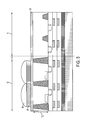
- FIG. 1 to FIG. 5 are cross-sectional diagrams illustrating an exemplary embodiment of forming backside illuminated image sensors.
- FIG. 6 to FIG. 8 are cross-sectional diagrams illustrating exemplary embodiments of forming an isolation structure in the pixel region of backside illuminated image sensor.
- cross-sectional diagrams of FIG. 1 to FIG. 5 illustrate an exemplary embodiment of a method of forming a backside illuminated image sensor.
- a substrate 10 having a front surface 10 a and a back surface 10 b is provided.
- the front surface 10 a is an active surface on which circuit designs will be formed.
- the substrate 10 may be silicon in a crystalline structure.
- the substrate 10 is a P-type substrate (e.g. a substrate doped with p-type dopants, such as boron or aluminum, by conventional processes such as diffusion or ion implantation).
- the substrate 10 may include a P + substrate, N + substrate, and/or other conductivities known in the art.
- the substrate 10 may include a silicon-on-insulator (SOI) substrate.
- SOI silicon-on-insulator
- the substrate 10 may include other elementary semiconductors such as germanium, or include a compound semiconductor such as, silicon carbide, gallium arsenide, indium arsenide, and indium phosphide.
- the substrate 10 includes a sub layer and an epitaxial (epi) layer formed on the sub layer, in which the sub layer is a P + layer and the epi layer is a P ⁇ layer.
- the substrate 10 is defined as a pixel region 12 and a peripheral region 14 .
- the pixel region 12 is for forming an array of pixels.
- the peripheral region 14 is for forming additional circuitry and input/output, which provides an operation environment for the pixels and/or supports external communications with the pixels.
- the peripheral region 14 is also known as a logic region as it may include logic circuitry associated with the pixels.
- a plurality of isolation structures 16 a and 16 b of different depths are formed in the substrate 10 of the pixel region 12 and the peripheral region 14 , respectively.
- the first isolation structure 16 a includes a first trench 18 a with a depth D 1 filled with a first insulating material layer 20 a .
- the remaining portion of the substrate 10 between the bottom of the first isolation structure 16 a and the back surface 10 b of the substrate 10 has a thickness T 1 , which will be removed in the subsequent thinning process.
- the first isolation structures 16 a at least partially isolate one pixel from a second pixel in the pixel region 12 .
- the depth D 1 is between approximately 1.0 ⁇ m and 10 ⁇ m, and the thickness T 1 is between approximately 600 ⁇ m and 900 ⁇ m. In an embodiment, the depth D 1 is between approximately 1.8 ⁇ m and 2.2 ⁇ m, and the thickness T 1 is between approximately 700 Angstroms and 800 Angstroms.
- the second isolation structure 16 b includes a second trench 18 b with a depth D 2 filled with a second insulating material layer 20 b for isolating one or more components formed in the peripheral region 14 .
- the depth D 2 is less than the depth D 1 . In an embodiment, the depth D 2 is less than approximately 1.0 ⁇ m. In an embodiment, the depth D 2 is between approximately 0.3 ⁇ m and 0.7 ⁇ m.
- the trenches 16 a and 16 b may be formed by processes known in the art such as photolithography patterning followed by RIE to form trenches in the patterned areas.
- the insulating material layer 20 a , 20 b may be formed by depositing material using chemical vapor deposition (CVD), plasma-enhanced chemical vapor deposition (PECVD), atmospheric pressure chemical vapor deposition (APCVD), low-pressure CVD (LPCVD), high density plasma CVD (HDPCVD), atomic layer CVD (ALCVD), sub-atmospheric CVD (SACVD), and/or other processes known in the art.
- the insulating material layer 20 a , 20 b is silicon oxide.
- the oxide is deposited by either HDPCVD or SACVD.
- the layer 20 a , 20 b may fill, partially or entirely, the trench 16 a , 16 b formed in the pixel region 12 and/or the peripheral region 14 .
- the layer is planarized by a chemical mechanical polish (CMP) process so that a substantially planar surface of the substrate 10 is provided.
- CMP chemical mechanical polish
- FIG. 2 illustrated is a step for fabricating image sensor elements 22 , interconnection structures 26 and passivation layers 28 on the substrate 10 .
- Circuit design is formed on the front surface 10 a of the substrate 10 .
- the circuit design includes sensor elements, transistors, metal interconnects, metal contacts, metal pads, and other circuitry, and the metal interconnects are formed inside a dielectric layer and/or a passivation layer. It is understood that conventional processes and equipment are used to fabricate the sensor elements, transistors, metal interconnects, metal contacts, metal pads, and other circuitry.
- One or more sensor elements 22 are formed on the pixel region 12 of the substrate 10 . In one embodiment, the sensor elements 22 may be disposed over the active surface and extended into the substrate 10 .
- the sensor elements 22 each may comprise a light-sensing region (or photo-sensing region) which may be a doped region having n-type and/or p-type dopants formed in the substrate 10 by a method such as diffusion or ion implantation.
- the sensor elements 22 may include photodiodes, pinned layer photodiodes, non-pinned layer photodiodes, reset transistors, source follower transistors, transfer transistors, select transistors, complimentary metal-oxide-semiconductor (CMOS) image sensors, charged coupling device (CCD) sensors, active pixel sensors, passive pixel sensors, other sensors diffused or otherwise formed in the substrate 10 , other active and/or passive features configured and coupled to provide proper functions such as imaging and/or sensing, and/or combinations thereof.
- CMOS complimentary metal-oxide-semiconductor
- CCD charged coupling device
- active pixel sensors passive pixel sensors
- other sensors diffused or otherwise formed in the substrate 10 other active and/or passive features configured and coupled to provide proper functions such as imaging and/or sensing, and/or combinations thereof.
- the sensor elements 22 may comprise conventional and/or future-developed image sensing devices.
- the sensor elements 22 may comprise a plurality of pixels disposed in a sensor array or other proper configuration. The
- one group of sensor pixels may be CMOS image sensors and another group of sensor pixels may be passive sensors.
- the sensor elements 22 may comprise color image sensors and/or monochromatic image sensors.
- additional circuitry and input/outputs are provided adjacent to the sensor elements 22 for providing an operation environment for the sensor elements 22 and for supporting external communications with the sensor elements 22 .
- the sensor elements 22 may further comprise or be coupled to components such as an electric circuit so that the sensor elements 22 are operable to provide a proper response to illuminated light.
- each of the sensor elements 22 may be configured to correspond with specific light wavelengths, such as a sensor element for sensing a red light wavelength, a sensor element for sensing a green light wavelength, and a sensor element for sensing a blue light wavelength.
- Multi-layer interconnection structure 26 including the metal interconnects, metal contacts and other circuitry are provided inside a plurality of inter-layer dielectric layers 24 formed on the substrate 10 .
- the interconnection structure 26 is coupled to the sensor elements 22 and other electric units formed in the substrate 10 .
- the interconnection structure 26 includes various metal features, and contact features configured between metal layers and the substrate 10 .
- the interconnection structure 26 further includes vias each configured between adjacent metal layers, coupling adjacent metal layers to one another.
- the interconnection structure 26 includes copper.
- the interconnection structure 26 may alternatively or collectively include other conductive materials such as copper alloy, titanium, titanium nitride, tantalum, tantalum nitride, tungsten, polysilicon, metal silicide, or combinations thereof.
- the metal silicide may include nickel silicide, cobalt silicide, tungsten silicide, tantalum silicide, titanium silicide, platinum silicide, erbium silicide, palladium silicide, or combinations thereof.
- the interconnection structure 26 may include multiple-layer structures, such as a barrier layer, a copper seed layer, and bulk copper. In one example, the top metal layer includes aluminum and the rest of the metal layers include copper.
- the interconnection structure 26 may be formed by a technique such as chemical vapor deposition, physical vapor deposition (PVD or sputtering), plating, other suitable processes, or combinations thereof. For example, PVD may be used to form a copper seed layer, and then a plating process may be employed to deposit bulk copper for interconnection.
- the metal layers in FIG. 2 are only for example and simplicity. In various embodiments, the interconnection structure 26 may include less or more than three metal layers.
- the inter-layer dielectric layer 24 is disposed on substrate 10 to isolate the interconnection structure 26 .
- Various etch stop/barrier layers may be interposed between adjacent inter-layer dielectric layers 24 for providing an etch stop function utilized during damascene processes or a barrier function to eliminate moisture diffusion to the interconnection structure 26 and copper migration to the inter-layer dielectric layers 24 .
- the stop/barrier layers may include silicon nitride, silicon oxynitride, or other suitable materials.
- the inter-layer dielectric layer 24 may include silicon dioxide such as undoped silica glass (USG), silicon nitride, silicon oxynitride, polyimide, spin-on glass (SOG), fluoride-doped silicate glass (FSG), carbon doped silicon oxide such as SiCOH, BLACK DIAMOND® (Applied Materials of Santa Clara, Calif.), XEROGELTM, AEROGELTM, amorphous fluorinated carbon, Parylene, BCB (bis-benzocyclobutenes), SILKTM (Dow Chemical, Midland, Mich.), and/or other suitable materials.
- the inter-layer dielectric layer 24 may be formed by any technique including spin-on, CVD, sputtering, or other suitable processes.
- PE plasma enhanced
- TEOS tetraethoxysilane
- HDP high density plasma
- the interconnection structure 26 and the inter-layer dielectric layer 24 may be formed in an integrated process referred to as a damascene process, such as a dual damascene process or a single damascene process.
- a passivation layer 28 is provided on the inter-layer dielectric layer 24 to substantially cover the devices and seal the device from moisture and other contamination.
- the passivation layer 28 includes silicon oxide, silicon nitride, or the combinations thereof. Another passivation layers may be provided for enhanced passivation and adhesion.
- the passivation layer 28 comprises a first silicon oxide layer, a second silicon nitride layer, and a third silicon oxide layer successively deposited on the inter-layer dielectric layer 24 .
- the carrier substrate 30 may be coated by an adhesive layer, depending on the bonding method used.
- the carrier substrate 30 may provide protection for the various features formed on the substrate 10 .
- the carrier substrate 30 may also provide mechanical strength and support for subsequent processes.
- the carrier substrate 30 may comprise any suitable material, such as silicon wafer and/or glass.
- the carrier substrate 30 is p + -type silicon substrate. Referring to FIG.
- a thinning process e.g., grinding and/or etching is performed on the back surface 10 b to remove the remaining portion of the substrate 10 , which stops on the bottom of the first isolation structure 16 a in the pixel region 12 , re-exposing the bottom of the first isolation structures 16 a in the pixel region 12 .
- the thinning process removes the remaining portion of thickness T 1 from the back surface 10 b of the substrate 10 , leaving a substrate thickness T 2 of the thinned substrate 10 .
- the substrate thickness is about 1 ⁇ 10 ⁇ m. This can make the device thin enough to allow the radiation incident on the back surface 10 b of the substrate 10 to reach the sensor elements.
- processing of the back surface 10 b of the substrate 10 is performed.
- An anti-reflective coating (ARC) layer 32 is formed on the back surface 10 b of the substrate 10 .
- the ARC layer 32 further reduces the reflection of incident light from the back surface 10 b of the substrate 10 .
- a color filter 34 is formed overlying the ARC layer 32 to filter light incident reaching the back surface 10 b of the substrate 10 .
- the color filter layer 34 may include a plurality of color filters arranged in a matrix at positions corresponding to the sensor elements 22 . In order to obtain images, the color filter layer 34 may transmit a light beam of a given color so that the light beam can reach the sensor elements 22 .
- the color filter layer 34 may include red (R), green (G), and blue (B) color filters arranged in a Bayer pattern, for example.
- one or more micro lenses 36 are disposed above the color filter 34 and may correspond to the plurality of sensor elements 22 .
- the micro lenses 36 may change the path of light incident on an area other than the sensor elements 22 such that the light may be focused onto the sensor elements 22 .
- the backside-illuminated image sensor includes a substrate 10 having a pixel region 12 and a peripheral region 14 .
- a plurality of pixels is formed on the substrate 10 of the pixel region 12 .
- the pixels include sensor elements 22 such as a photo detector and one or more transistors.
- the peripheral region 14 includes additional circuitry and input/outputs.
- a plurality of first isolation structures 16 a of a depth D 1 is formed in the substrate 10 of the pixel region 12 and a plurality of second isolation structures 16 b of a depth D 2 is formed in the substrate 10 of the peripheral region 14 .
- Image sensor elements 22 are formed on the front surface 10 a in the pixel region 12 , logic circuitry is formed on the front surface 10 a in the peripheral region 14 , and interconnection structures 26 are formed over the sensor elements 22 and the logic circuitry.
- the back surface 10 b is thinned downed to expose the bottom of the first isolation structures 16 a , leaving the thinned substrate 10 of a substrate thickness T 2 .
- Backside processes including forming an ARC layer 32 , a color filter 34 and micro lenses 36 are performed on the back surface 10 b of the thinned substrate 10 .
- this disclosure provides the first isolation structures 16 a in the pixel region 12 with the depth D 1 that is greater than the depth D 2 of the second isolation structures 16 b in the peripheral region 14 , and substantially equal to the substrate thickness T 2 of the thinned substrate 10 .
- the first isolation structure 16 a passing through the thinned substrate 10 can provide good isolation performance to reduce leakage (e.g., substrate electrical path) in the pixel region 12 , and provide good light efficiency to enhance Quantum Efficiency and prevent cross talk.
- the bottom of first isolation structure 16 a can serve as a stop layer.
- FIG. 6 to FIG. 8 illustrate incremental modifications of the first isolation structures 16 a corresponding to the step of FIG. 1
- an implant region 40 is formed through an ion implantation process 42 in the substrate 10 adjacent to each the first isolation structure 16 a to provide isolation between sensor elements 22 .
- the implant region 40 is formed adjacent the sidewalls of the upper portion 16 a 1 of the first isolation structure 16 a .
- the implant region 40 is formed adjacent the sidewalls of the upper portion 16 a 1 and the lower portion 16 a 2 of the first isolation structure 16 a .
- FIG. 6 the implant region 40 is formed through an ion implantation process 42 in the substrate 10 adjacent to each the first isolation structure 16 a to provide isolation between sensor elements 22 .
- the implant region 40 is formed adjacent the sidewalls of the upper portion 16 a 1 of the first isolation structure 16 a .
- the implant region 40 is formed adjacent the sidewalls of the upper portion 16 a 1 and the lower portion 16 a 2 of the first isolation structure 16 a .
- the implant region 40 is formed not only adjacent the sidewalls of the first isolation structure 16 a , but also underlying the bottom portion 16 a 3 of the first isolation structure 16 a .
- the implant region 40 is a p-type region formed by doping the substrate 10 with p-type dopants such as, boron, BF 2 , or other suitable material known in the art. The doping may be accomplished by conventional processes known in the art such as ion implantation or diffusion in a region defined by conventional photolithography processes.
- the implant region 40 provides electrical grounding and reduces leakage current of the sensor elements 22 and at the same time improves photo sensitivity, especially for blue light. Accordingly, quantum efficiency (percentage of incident light that is detected) of the backside illuminated image sensor is improved.
- the backside illuminated image sensor includes a substrate, where the substrate includes a pixel region and a peripheral region.
- the substrate further includes a front surface and a back surface.
- the backside illuminated image sensor further includes a first isolation structure formed in the pixel region of the substrate, where a bottom of the first isolation structure is exposed at the back surface of the substrate.
- the backside illuminated image sensor includes a second isolation structure formed in the peripheral region of the substrate, where the second isolation structure has a depth less than a depth of the first isolation structure.
- the backside illuminated image sensor includes an implant region adjacent to at least a portion of sidewalls of each isolation structure in the pixel region, where the portion of the sidewalls are located closer to the back surface than a top surface of the substrate, and where the second isolation structure is free of the implant region.
- the backside illuminated image sensor includes a substrate having a first surface and a light receiving surface, where the first surface includes a sensor element.
- the backside illuminated image sensor further includes first isolation structure passing through the substrate, where the first isolation structure has a first depth and a bottom of the first isolation structure is exposed at the light receiving surface of the substrate.
- the backside illuminated image sensor further includes a sensor element in the first surface of the substrate.
- the backside illuminated image sensor includes a color filter overlying the light receiving surface of the substrate.
- the backside illuminated image sensor includes a second isolation structure in the substrate, wherein the second isolation structure has a second depth less than the first depth.
- the backside illuminated image sensor additionally includes an implant region adjacent to at least a portion of sidewalls of each first isolation structure, wherein the portion of the sidewalls are located closer to the light receiving surface than the first surface of the substrate, wherein the second isolation structure is free of the implant region.
- the method of making a backside illuminated image sensor includes forming a first isolation structure in a pixel region of a substrate, where the substrate includes the pixel region and a peripheral region, and where the substrate includes a front surface and a back surface.
- the method of making a backside illuminated image sensor further includes forming a second isolation structure in the peripheral region of the substrate, where the second isolation structure has a depth less than a depth of the first isolation structure.
- the method of making a backside illuminated image sensor includes exposing a bottom of the first isolation structure at the back surface of the substrate.
- the method of making a backside illuminated image sensor includes forming an implant region adjacent to at least a portion of sidewalls of at least one isolation structure in the pixel region, where the second isolation structure is free of any implant region.
Abstract
Description
Claims (20)
Priority Applications (2)
| Application Number | Priority Date | Filing Date | Title |
|---|---|---|---|
| US14/172,053 US8946847B2 (en) | 2009-04-23 | 2014-02-04 | Backside illuminated image sensors and method of making the same |
| US14/587,687 US9257326B2 (en) | 2009-04-23 | 2014-12-31 | Method of making backside illuminated image sensors |
Applications Claiming Priority (3)
| Application Number | Priority Date | Filing Date | Title |
|---|---|---|---|
| US17199809P | 2009-04-23 | 2009-04-23 | |
| US12/766,130 US8674469B2 (en) | 2009-04-23 | 2010-04-23 | Isolation structure for backside illuminated image sensor |
| US14/172,053 US8946847B2 (en) | 2009-04-23 | 2014-02-04 | Backside illuminated image sensors and method of making the same |
Related Parent Applications (1)
| Application Number | Title | Priority Date | Filing Date |
|---|---|---|---|
| US12/766,130 Continuation US8674469B2 (en) | 2009-04-23 | 2010-04-23 | Isolation structure for backside illuminated image sensor |
Related Child Applications (1)
| Application Number | Title | Priority Date | Filing Date |
|---|---|---|---|
| US14/587,687 Division US9257326B2 (en) | 2009-04-23 | 2014-12-31 | Method of making backside illuminated image sensors |
Publications (2)
| Publication Number | Publication Date |
|---|---|
| US20140151835A1 US20140151835A1 (en) | 2014-06-05 |
| US8946847B2 true US8946847B2 (en) | 2015-02-03 |
Family
ID=42991365
Family Applications (3)
| Application Number | Title | Priority Date | Filing Date |
|---|---|---|---|
| US12/766,130 Active 2031-01-10 US8674469B2 (en) | 2009-04-23 | 2010-04-23 | Isolation structure for backside illuminated image sensor |
| US14/172,053 Active US8946847B2 (en) | 2009-04-23 | 2014-02-04 | Backside illuminated image sensors and method of making the same |
| US14/587,687 Expired - Fee Related US9257326B2 (en) | 2009-04-23 | 2014-12-31 | Method of making backside illuminated image sensors |
Family Applications Before (1)
| Application Number | Title | Priority Date | Filing Date |
|---|---|---|---|
| US12/766,130 Active 2031-01-10 US8674469B2 (en) | 2009-04-23 | 2010-04-23 | Isolation structure for backside illuminated image sensor |
Family Applications After (1)
| Application Number | Title | Priority Date | Filing Date |
|---|---|---|---|
| US14/587,687 Expired - Fee Related US9257326B2 (en) | 2009-04-23 | 2014-12-31 | Method of making backside illuminated image sensors |
Country Status (1)
| Country | Link |
|---|---|
| US (3) | US8674469B2 (en) |
Families Citing this family (27)
| Publication number | Priority date | Publication date | Assignee | Title |
|---|---|---|---|---|
| US8956909B2 (en) * | 2010-07-16 | 2015-02-17 | Unimicron Technology Corporation | Method of fabricating an electronic device comprising photodiode |
| KR101095945B1 (en) | 2011-02-03 | 2011-12-19 | 테쎄라 노쓰 아메리카, 아이엔씨. | Bsi image sensor package with embedded absorber for even reception of different wavelengths |
| KR101133154B1 (en) | 2011-02-03 | 2012-04-06 | 디지털옵틱스 코포레이션 이스트 | Bsi image sensor package with variable-height silicon for even reception of different wavelengths |
| US8461683B2 (en) * | 2011-04-01 | 2013-06-11 | Intel Corporation | Self-forming, self-aligned barriers for back-end interconnects and methods of making same |
| US8853811B2 (en) * | 2011-11-07 | 2014-10-07 | Taiwan Semiconductor Manufacturing Company, Ltd. | Image sensor trench isolation with conformal doping |
| US9269730B2 (en) * | 2012-02-09 | 2016-02-23 | Semiconductor Components Industries, Llc | Imaging systems with backside isolation trenches |
| US8652868B2 (en) * | 2012-03-01 | 2014-02-18 | Taiwan Semiconductor Manufacturing Company, Ltd. | Implanting method for forming photodiode |
| US8941204B2 (en) * | 2012-04-27 | 2015-01-27 | Taiwan Semiconductor Manufacturing Company, Ltd. | Apparatus and method for reducing cross talk in image sensors |
| US9040891B2 (en) * | 2012-06-08 | 2015-05-26 | Taiwan Semiconductor Manufacturing Company, Ltd. | Image device and methods of forming the same |
| KR102023623B1 (en) * | 2012-07-03 | 2019-09-23 | 삼성전자 주식회사 | Methods of Fabricating Semiconductor Devices |
| US8969997B2 (en) * | 2012-11-14 | 2015-03-03 | Taiwan Semiconductor Manufacturing Company, Ltd. | Isolation structures and methods of forming the same |
| KR102083402B1 (en) | 2013-02-25 | 2020-03-02 | 삼성전자주식회사 | Image sensor and method of forming the same |
| US9006080B2 (en) * | 2013-03-12 | 2015-04-14 | Taiwan Semiconductor Manufacturing Company, Ltd. | Varied STI liners for isolation structures in image sensing devices |
| CN103337507B (en) * | 2013-06-27 | 2017-04-26 | 上海华虹宏力半导体制造有限公司 | Image sensor and forming method thereof |
| KR102318461B1 (en) * | 2013-11-06 | 2021-10-28 | 소니그룹주식회사 | Semiconductor device, solid-state imaging element, and electronic instrument |
| US9780137B2 (en) * | 2013-11-25 | 2017-10-03 | Taiwan Semiconductor Manufacturing Co., Ltd. | Mechanisms for forming image-sensor device with epitaxial isolation feature |
| KR102367384B1 (en) * | 2015-01-13 | 2022-02-25 | 삼성전자주식회사 | Image sensor and method of forming the same |
| KR102368573B1 (en) * | 2015-01-14 | 2022-03-02 | 삼성전자주식회사 | Image sensor |
| US9876045B2 (en) * | 2015-05-06 | 2018-01-23 | Cista System Corp. | Back side illuminated CMOS image sensor arrays |
| US10515845B2 (en) * | 2017-11-09 | 2019-12-24 | Taiwan Semiconductor Manufacturing Company Ltd. | Semiconductor structure including isolations and method for manufacturing the same |
| CN109103211A (en) * | 2018-08-24 | 2018-12-28 | 德淮半导体有限公司 | Back side illumination image sensor and forming method thereof |
| CN112041988A (en) * | 2019-04-28 | 2020-12-04 | 深圳市大疆创新科技有限公司 | Image sensor chip, manufacturing method, image sensor, and imaging device |
| US11348958B2 (en) | 2019-05-16 | 2022-05-31 | Taiwan Semiconductor Manufacturing Company Ltd. | Image sensing device with grid structure and fabrication method thereof |
| KR20200141345A (en) * | 2019-06-10 | 2020-12-18 | 삼성전자주식회사 | Image sensor comprising auto focus pixel |
| KR20220043943A (en) * | 2020-09-28 | 2022-04-06 | 삼성전자주식회사 | Image sensor |
| CN113629081A (en) * | 2021-07-15 | 2021-11-09 | 华虹半导体(无锡)有限公司 | Method for manufacturing image sensor |
| CN117393502B (en) * | 2023-12-12 | 2024-03-01 | 合肥晶合集成电路股份有限公司 | Semiconductor structure and manufacturing method thereof |
Citations (16)
| Publication number | Priority date | Publication date | Assignee | Title |
|---|---|---|---|---|
| US4377817A (en) | 1979-03-19 | 1983-03-22 | Semiconductor Research Foundation | Semiconductor image sensors |
| US5960276A (en) | 1998-09-28 | 1999-09-28 | Taiwan Semiconductor Manufacturing Company, Ltd. | Using an extra boron implant to improve the NMOS reverse narrow width effect in shallow trench isolation process |
| US6852562B1 (en) | 2003-12-05 | 2005-02-08 | Eastman Kodak Company | Low-cost method of forming a color imager |
| US7154136B2 (en) | 2004-02-20 | 2006-12-26 | Micron Technology, Inc. | Isolation structures for preventing photons and carriers from reaching active areas and methods of formation |
| US20070194356A1 (en) | 2006-01-31 | 2007-08-23 | Chang-Rok Moon | Image sensor having improved sensitivity and decreased crosstalk and method of fabricating same |
| US7354812B2 (en) | 2004-09-01 | 2008-04-08 | Micron Technology, Inc. | Multiple-depth STI trenches in integrated circuit fabrication |
| US7492027B2 (en) | 2004-02-20 | 2009-02-17 | Micron Technology, Inc. | Reduced crosstalk sensor and method of formation |
| US20090200625A1 (en) | 2008-02-08 | 2009-08-13 | Omnivision Technologies, Inc. | Backside illuminated image sensor having deep light reflective trenches |
| US20090250778A1 (en) | 2008-04-04 | 2009-10-08 | Canon Kabushiki Kaisha | Photoelectric conversion device, imaging system, photoelectric conversion device designing method, and photoelectric conversion device manufacturing method |
| US7741141B2 (en) | 2006-03-02 | 2010-06-22 | Icemos Technology Ltd. | Photodiode having increased proportion of light-sensitive area to light-insensitive area |
| US7768090B2 (en) * | 2007-03-20 | 2010-08-03 | Panasonic Corporation | Semiconductor photodetector device |
| US7768085B2 (en) | 2005-10-11 | 2010-08-03 | Icemos Technology Ltd. | Photodetector array using isolation diffusions as crosstalk inhibitors between adjacent photodiodes |
| US20100252870A1 (en) | 2009-04-03 | 2010-10-07 | Taiwan Semiconductor Manufacturing Company, Ltd. | Dual shallow trench isolation and related applications |
| US7838956B2 (en) * | 2008-12-17 | 2010-11-23 | Eastman Kodak Company | Back illuminated sensor with low crosstalk |
| US20110163363A1 (en) | 2008-08-28 | 2011-07-07 | Ui-Sik Kim | COMS image sensors and methods of manufacturing the same |
| US8237206B2 (en) | 2008-08-12 | 2012-08-07 | United Microelectronics Corp. | CMOS image sensor, method of making the same, and method of suppressing dark leakage and crosstalk for CMOS image sensor |
Family Cites Families (6)
| Publication number | Priority date | Publication date | Assignee | Title |
|---|---|---|---|---|
| US7102184B2 (en) * | 2003-06-16 | 2006-09-05 | Micron Technology, Inc. | Image device and photodiode structure |
| JP2009206356A (en) * | 2008-02-28 | 2009-09-10 | Toshiba Corp | Solid-state imaging device and manufacturing method thereof |
| EP2109143B1 (en) * | 2008-04-09 | 2013-05-29 | Sony Corporation | Solid-state imaging device, production method thereof, and electronic device |
| US20100006908A1 (en) * | 2008-07-09 | 2010-01-14 | Brady Frederick T | Backside illuminated image sensor with shallow backside trench for photodiode isolation |
| US8531565B2 (en) * | 2009-02-24 | 2013-09-10 | Taiwan Semiconductor Manufacturing Company, Ltd. | Front side implanted guard ring structure for backside illuminated image sensor |
| US8389377B2 (en) * | 2010-04-02 | 2013-03-05 | Taiwan Semiconductor Manufacturing Company, Ltd. | Sensor element isolation in a backside illuminated image sensor |
-
2010
- 2010-04-23 US US12/766,130 patent/US8674469B2/en active Active
-
2014
- 2014-02-04 US US14/172,053 patent/US8946847B2/en active Active
- 2014-12-31 US US14/587,687 patent/US9257326B2/en not_active Expired - Fee Related
Patent Citations (18)
| Publication number | Priority date | Publication date | Assignee | Title |
|---|---|---|---|---|
| US4377817A (en) | 1979-03-19 | 1983-03-22 | Semiconductor Research Foundation | Semiconductor image sensors |
| US5960276A (en) | 1998-09-28 | 1999-09-28 | Taiwan Semiconductor Manufacturing Company, Ltd. | Using an extra boron implant to improve the NMOS reverse narrow width effect in shallow trench isolation process |
| US6852562B1 (en) | 2003-12-05 | 2005-02-08 | Eastman Kodak Company | Low-cost method of forming a color imager |
| US7154136B2 (en) | 2004-02-20 | 2006-12-26 | Micron Technology, Inc. | Isolation structures for preventing photons and carriers from reaching active areas and methods of formation |
| US7400004B2 (en) | 2004-02-20 | 2008-07-15 | Micron Technology, Inc. | Isolation structures for preventing photons and carriers from reaching active areas and methods of formation |
| US7492027B2 (en) | 2004-02-20 | 2009-02-17 | Micron Technology, Inc. | Reduced crosstalk sensor and method of formation |
| US7354812B2 (en) | 2004-09-01 | 2008-04-08 | Micron Technology, Inc. | Multiple-depth STI trenches in integrated circuit fabrication |
| US7768085B2 (en) | 2005-10-11 | 2010-08-03 | Icemos Technology Ltd. | Photodetector array using isolation diffusions as crosstalk inhibitors between adjacent photodiodes |
| US7518172B2 (en) | 2006-01-31 | 2009-04-14 | Samsung Electronics Co., Ltd. | Image sensor having improved sensitivity and decreased crosstalk and method of fabricating same |
| US20070194356A1 (en) | 2006-01-31 | 2007-08-23 | Chang-Rok Moon | Image sensor having improved sensitivity and decreased crosstalk and method of fabricating same |
| US7741141B2 (en) | 2006-03-02 | 2010-06-22 | Icemos Technology Ltd. | Photodiode having increased proportion of light-sensitive area to light-insensitive area |
| US7768090B2 (en) * | 2007-03-20 | 2010-08-03 | Panasonic Corporation | Semiconductor photodetector device |
| US20090200625A1 (en) | 2008-02-08 | 2009-08-13 | Omnivision Technologies, Inc. | Backside illuminated image sensor having deep light reflective trenches |
| US20090250778A1 (en) | 2008-04-04 | 2009-10-08 | Canon Kabushiki Kaisha | Photoelectric conversion device, imaging system, photoelectric conversion device designing method, and photoelectric conversion device manufacturing method |
| US8237206B2 (en) | 2008-08-12 | 2012-08-07 | United Microelectronics Corp. | CMOS image sensor, method of making the same, and method of suppressing dark leakage and crosstalk for CMOS image sensor |
| US20110163363A1 (en) | 2008-08-28 | 2011-07-07 | Ui-Sik Kim | COMS image sensors and methods of manufacturing the same |
| US7838956B2 (en) * | 2008-12-17 | 2010-11-23 | Eastman Kodak Company | Back illuminated sensor with low crosstalk |
| US20100252870A1 (en) | 2009-04-03 | 2010-10-07 | Taiwan Semiconductor Manufacturing Company, Ltd. | Dual shallow trench isolation and related applications |
Also Published As
| Publication number | Publication date |
|---|---|
| US20140151835A1 (en) | 2014-06-05 |
| US8674469B2 (en) | 2014-03-18 |
| US20100270636A1 (en) | 2010-10-28 |
| US20150111334A1 (en) | 2015-04-23 |
| US9257326B2 (en) | 2016-02-09 |
Similar Documents
| Publication | Publication Date | Title |
|---|---|---|
| US9257326B2 (en) | Method of making backside illuminated image sensors | |
| US11495632B2 (en) | Back side illuminated image sensor with deep trench isolation structures and self-aligned color filters | |
| US11735619B2 (en) | Semiconductor image sensor device having back side illuminated image sensors with embedded color filters | |
| KR101897433B1 (en) | Method and apparatus for backside illumination sensor | |
| USRE46123E1 (en) | Solid-state image sensor and method of manufacturing the same | |
| US20170133414A1 (en) | Dti for bsi image sensor | |
| US9548329B2 (en) | Backside illuminated image sensor and method of manufacturing the same | |
| JP2010258157A (en) | Solid-state imaging device and method of manufacturing the same | |
| US8980674B2 (en) | Image sensor with improved dark current performance | |
| TWI685093B (en) | Image sensor, semiconductor image sensor, and method of manufacturing semiconductor image sensor | |
| KR20110079323A (en) | Image sensor and method for manufacturing the same | |
| US8106429B2 (en) | Image sensor and manufacturing method thereof | |
| US20100181635A1 (en) | Method and structure for reducing cross-talk in image sensor devices | |
| US8951826B2 (en) | Method for increasing photodiode full well capacity | |
| US8460979B2 (en) | Method of fabricating a backside illuminated image sensor | |
| KR20210053264A (en) | Light blocking layer for image sensor device |
Legal Events
| Date | Code | Title | Description |
|---|---|---|---|
| AS | Assignment |
Owner name: TAIWAN SEMICONDUCTOR MANUFACTURING COMPANY, LTD., Free format text: ASSIGNMENT OF ASSIGNORS INTEREST;ASSIGNORS:HUANG, KUAN-CHIEH;WU, CHIH-JEN;HUANG, CHEN-MING;AND OTHERS;REEL/FRAME:032131/0285 Effective date: 20100511 |
|
| STCF | Information on status: patent grant |
Free format text: PATENTED CASE |
|
| MAFP | Maintenance fee payment |
Free format text: PAYMENT OF MAINTENANCE FEE, 4TH YEAR, LARGE ENTITY (ORIGINAL EVENT CODE: M1551) Year of fee payment: 4 |
|
| MAFP | Maintenance fee payment |
Free format text: PAYMENT OF MAINTENANCE FEE, 8TH YEAR, LARGE ENTITY (ORIGINAL EVENT CODE: M1552); ENTITY STATUS OF PATENT OWNER: LARGE ENTITY Year of fee payment: 8 |