US9024329B2 - Silicon carbide trench MOSFET having reduced on-resistance, increased dielectric withstand voltage, and reduced threshold voltage - Google Patents
Silicon carbide trench MOSFET having reduced on-resistance, increased dielectric withstand voltage, and reduced threshold voltage Download PDFInfo
- Publication number
- US9024329B2 US9024329B2 US14/049,810 US201314049810A US9024329B2 US 9024329 B2 US9024329 B2 US 9024329B2 US 201314049810 A US201314049810 A US 201314049810A US 9024329 B2 US9024329 B2 US 9024329B2
- Authority
- US
- United States
- Prior art keywords
- semiconductor layer
- semiconductor device
- trench
- region
- semiconductor
- Prior art date
- Legal status (The legal status is an assumption and is not a legal conclusion. Google has not performed a legal analysis and makes no representation as to the accuracy of the status listed.)
- Active
Links
- HBMJWWWQQXIZIP-UHFFFAOYSA-N silicon carbide Chemical compound [Si+]#[C-] HBMJWWWQQXIZIP-UHFFFAOYSA-N 0.000 title claims description 13
- 229910010271 silicon carbide Inorganic materials 0.000 title claims description 13
- 239000004065 semiconductor Substances 0.000 claims abstract description 231
- 239000012535 impurity Substances 0.000 claims abstract description 47
- 230000015556 catabolic process Effects 0.000 claims description 16
- 230000007423 decrease Effects 0.000 claims description 2
- 230000000149 penetrating effect Effects 0.000 claims description 2
- 239000010410 layer Substances 0.000 description 112
- 239000000758 substrate Substances 0.000 description 7
- 150000002500 ions Chemical class 0.000 description 6
- 230000000694 effects Effects 0.000 description 5
- PXHVJJICTQNCMI-UHFFFAOYSA-N Nickel Chemical compound [Ni] PXHVJJICTQNCMI-UHFFFAOYSA-N 0.000 description 4
- 229910052782 aluminium Inorganic materials 0.000 description 3
- 239000011229 interlayer Substances 0.000 description 3
- 238000004519 manufacturing process Methods 0.000 description 3
- VYPSYNLAJGMNEJ-UHFFFAOYSA-N Silicium dioxide Chemical compound O=[Si]=O VYPSYNLAJGMNEJ-UHFFFAOYSA-N 0.000 description 2
- XAGFODPZIPBFFR-UHFFFAOYSA-N aluminium Chemical compound [Al] XAGFODPZIPBFFR-UHFFFAOYSA-N 0.000 description 2
- -1 aluminum ion Chemical class 0.000 description 2
- 239000000470 constituent Substances 0.000 description 2
- 229910052759 nickel Inorganic materials 0.000 description 2
- 229910052796 boron Inorganic materials 0.000 description 1
- 239000013078 crystal Substances 0.000 description 1
- 238000010586 diagram Methods 0.000 description 1
- 238000000034 method Methods 0.000 description 1
- 235000012239 silicon dioxide Nutrition 0.000 description 1
- 239000000377 silicon dioxide Substances 0.000 description 1
Images


Classifications
-
- H—ELECTRICITY
- H01—ELECTRIC ELEMENTS
- H01L—SEMICONDUCTOR DEVICES NOT COVERED BY CLASS H10
- H01L29/00—Semiconductor devices adapted for rectifying, amplifying, oscillating or switching, or capacitors or resistors with at least one potential-jump barrier or surface barrier, e.g. PN junction depletion layer or carrier concentration layer; Details of semiconductor bodies or of electrodes thereof ; Multistep manufacturing processes therefor
- H01L29/66—Types of semiconductor device ; Multistep manufacturing processes therefor
- H01L29/68—Types of semiconductor device ; Multistep manufacturing processes therefor controllable by only the electric current supplied, or only the electric potential applied, to an electrode which does not carry the current to be rectified, amplified or switched
- H01L29/76—Unipolar devices, e.g. field effect transistors
- H01L29/772—Field effect transistors
- H01L29/78—Field effect transistors with field effect produced by an insulated gate
- H01L29/7801—DMOS transistors, i.e. MISFETs with a channel accommodating body or base region adjoining a drain drift region
- H01L29/7802—Vertical DMOS transistors, i.e. VDMOS transistors
- H01L29/7813—Vertical DMOS transistors, i.e. VDMOS transistors with trench gate electrode, e.g. UMOS transistors
-
- H—ELECTRICITY
- H01—ELECTRIC ELEMENTS
- H01L—SEMICONDUCTOR DEVICES NOT COVERED BY CLASS H10
- H01L29/00—Semiconductor devices adapted for rectifying, amplifying, oscillating or switching, or capacitors or resistors with at least one potential-jump barrier or surface barrier, e.g. PN junction depletion layer or carrier concentration layer; Details of semiconductor bodies or of electrodes thereof ; Multistep manufacturing processes therefor
- H01L29/02—Semiconductor bodies ; Multistep manufacturing processes therefor
- H01L29/06—Semiconductor bodies ; Multistep manufacturing processes therefor characterised by their shape; characterised by the shapes, relative sizes, or dispositions of the semiconductor regions ; characterised by the concentration or distribution of impurities within semiconductor regions
- H01L29/10—Semiconductor bodies ; Multistep manufacturing processes therefor characterised by their shape; characterised by the shapes, relative sizes, or dispositions of the semiconductor regions ; characterised by the concentration or distribution of impurities within semiconductor regions with semiconductor regions connected to an electrode not carrying current to be rectified, amplified or switched and such electrode being part of a semiconductor device which comprises three or more electrodes
- H01L29/1095—Body region, i.e. base region, of DMOS transistors or IGBTs
-
- H—ELECTRICITY
- H01—ELECTRIC ELEMENTS
- H01L—SEMICONDUCTOR DEVICES NOT COVERED BY CLASS H10
- H01L29/00—Semiconductor devices adapted for rectifying, amplifying, oscillating or switching, or capacitors or resistors with at least one potential-jump barrier or surface barrier, e.g. PN junction depletion layer or carrier concentration layer; Details of semiconductor bodies or of electrodes thereof ; Multistep manufacturing processes therefor
- H01L29/02—Semiconductor bodies ; Multistep manufacturing processes therefor
- H01L29/12—Semiconductor bodies ; Multistep manufacturing processes therefor characterised by the materials of which they are formed
- H01L29/16—Semiconductor bodies ; Multistep manufacturing processes therefor characterised by the materials of which they are formed including, apart from doping materials or other impurities, only elements of Group IV of the Periodic System
- H01L29/1608—Silicon carbide
-
- H—ELECTRICITY
- H01—ELECTRIC ELEMENTS
- H01L—SEMICONDUCTOR DEVICES NOT COVERED BY CLASS H10
- H01L29/00—Semiconductor devices adapted for rectifying, amplifying, oscillating or switching, or capacitors or resistors with at least one potential-jump barrier or surface barrier, e.g. PN junction depletion layer or carrier concentration layer; Details of semiconductor bodies or of electrodes thereof ; Multistep manufacturing processes therefor
- H01L29/66—Types of semiconductor device ; Multistep manufacturing processes therefor
- H01L29/66007—Multistep manufacturing processes
- H01L29/66053—Multistep manufacturing processes of devices having a semiconductor body comprising crystalline silicon carbide
- H01L29/66068—Multistep manufacturing processes of devices having a semiconductor body comprising crystalline silicon carbide the devices being controllable only by the electric current supplied or the electric potential applied, to an electrode which does not carry the current to be rectified, amplified or switched, e.g. three-terminal devices
-
- H—ELECTRICITY
- H01—ELECTRIC ELEMENTS
- H01L—SEMICONDUCTOR DEVICES NOT COVERED BY CLASS H10
- H01L29/00—Semiconductor devices adapted for rectifying, amplifying, oscillating or switching, or capacitors or resistors with at least one potential-jump barrier or surface barrier, e.g. PN junction depletion layer or carrier concentration layer; Details of semiconductor bodies or of electrodes thereof ; Multistep manufacturing processes therefor
- H01L29/66—Types of semiconductor device ; Multistep manufacturing processes therefor
- H01L29/68—Types of semiconductor device ; Multistep manufacturing processes therefor controllable by only the electric current supplied, or only the electric potential applied, to an electrode which does not carry the current to be rectified, amplified or switched
- H01L29/70—Bipolar devices
- H01L29/72—Transistor-type devices, i.e. able to continuously respond to applied control signals
- H01L29/739—Transistor-type devices, i.e. able to continuously respond to applied control signals controlled by field-effect, e.g. bipolar static induction transistors [BSIT]
- H01L29/7393—Insulated gate bipolar mode transistors, i.e. IGBT; IGT; COMFET
- H01L29/7395—Vertical transistors, e.g. vertical IGBT
- H01L29/7396—Vertical transistors, e.g. vertical IGBT with a non planar surface, e.g. with a non planar gate or with a trench or recess or pillar in the surface of the emitter, base or collector region for improving current density or short circuiting the emitter and base regions
- H01L29/7397—Vertical transistors, e.g. vertical IGBT with a non planar surface, e.g. with a non planar gate or with a trench or recess or pillar in the surface of the emitter, base or collector region for improving current density or short circuiting the emitter and base regions and a gate structure lying on a slanted or vertical surface or formed in a groove, e.g. trench gate IGBT
-
- H—ELECTRICITY
- H01—ELECTRIC ELEMENTS
- H01L—SEMICONDUCTOR DEVICES NOT COVERED BY CLASS H10
- H01L29/00—Semiconductor devices adapted for rectifying, amplifying, oscillating or switching, or capacitors or resistors with at least one potential-jump barrier or surface barrier, e.g. PN junction depletion layer or carrier concentration layer; Details of semiconductor bodies or of electrodes thereof ; Multistep manufacturing processes therefor
- H01L29/02—Semiconductor bodies ; Multistep manufacturing processes therefor
- H01L29/06—Semiconductor bodies ; Multistep manufacturing processes therefor characterised by their shape; characterised by the shapes, relative sizes, or dispositions of the semiconductor regions ; characterised by the concentration or distribution of impurities within semiconductor regions
- H01L29/0603—Semiconductor bodies ; Multistep manufacturing processes therefor characterised by their shape; characterised by the shapes, relative sizes, or dispositions of the semiconductor regions ; characterised by the concentration or distribution of impurities within semiconductor regions characterised by particular constructional design considerations, e.g. for preventing surface leakage, for controlling electric field concentration or for internal isolations regions
- H01L29/0607—Semiconductor bodies ; Multistep manufacturing processes therefor characterised by their shape; characterised by the shapes, relative sizes, or dispositions of the semiconductor regions ; characterised by the concentration or distribution of impurities within semiconductor regions characterised by particular constructional design considerations, e.g. for preventing surface leakage, for controlling electric field concentration or for internal isolations regions for preventing surface leakage or controlling electric field concentration
- H01L29/0611—Semiconductor bodies ; Multistep manufacturing processes therefor characterised by their shape; characterised by the shapes, relative sizes, or dispositions of the semiconductor regions ; characterised by the concentration or distribution of impurities within semiconductor regions characterised by particular constructional design considerations, e.g. for preventing surface leakage, for controlling electric field concentration or for internal isolations regions for preventing surface leakage or controlling electric field concentration for increasing or controlling the breakdown voltage of reverse biased devices
- H01L29/0615—Semiconductor bodies ; Multistep manufacturing processes therefor characterised by their shape; characterised by the shapes, relative sizes, or dispositions of the semiconductor regions ; characterised by the concentration or distribution of impurities within semiconductor regions characterised by particular constructional design considerations, e.g. for preventing surface leakage, for controlling electric field concentration or for internal isolations regions for preventing surface leakage or controlling electric field concentration for increasing or controlling the breakdown voltage of reverse biased devices by the doping profile or the shape or the arrangement of the PN junction, or with supplementary regions, e.g. junction termination extension [JTE]
- H01L29/063—Reduced surface field [RESURF] pn-junction structures
- H01L29/0634—Multiple reduced surface field (multi-RESURF) structures, e.g. double RESURF, charge compensation, cool, superjunction (SJ), 3D-RESURF, composite buffer (CB) structures
-
- H—ELECTRICITY
- H01—ELECTRIC ELEMENTS
- H01L—SEMICONDUCTOR DEVICES NOT COVERED BY CLASS H10
- H01L29/00—Semiconductor devices adapted for rectifying, amplifying, oscillating or switching, or capacitors or resistors with at least one potential-jump barrier or surface barrier, e.g. PN junction depletion layer or carrier concentration layer; Details of semiconductor bodies or of electrodes thereof ; Multistep manufacturing processes therefor
- H01L29/40—Electrodes ; Multistep manufacturing processes therefor
- H01L29/41—Electrodes ; Multistep manufacturing processes therefor characterised by their shape, relative sizes or dispositions
- H01L29/423—Electrodes ; Multistep manufacturing processes therefor characterised by their shape, relative sizes or dispositions not carrying the current to be rectified, amplified or switched
- H01L29/42312—Gate electrodes for field effect devices
- H01L29/42316—Gate electrodes for field effect devices for field-effect transistors
- H01L29/4232—Gate electrodes for field effect devices for field-effect transistors with insulated gate
- H01L29/42364—Gate electrodes for field effect devices for field-effect transistors with insulated gate characterised by the insulating layer, e.g. thickness or uniformity
- H01L29/42368—Gate electrodes for field effect devices for field-effect transistors with insulated gate characterised by the insulating layer, e.g. thickness or uniformity the thickness being non-uniform
-
- H—ELECTRICITY
- H01—ELECTRIC ELEMENTS
- H01L—SEMICONDUCTOR DEVICES NOT COVERED BY CLASS H10
- H01L29/00—Semiconductor devices adapted for rectifying, amplifying, oscillating or switching, or capacitors or resistors with at least one potential-jump barrier or surface barrier, e.g. PN junction depletion layer or carrier concentration layer; Details of semiconductor bodies or of electrodes thereof ; Multistep manufacturing processes therefor
- H01L29/40—Electrodes ; Multistep manufacturing processes therefor
- H01L29/43—Electrodes ; Multistep manufacturing processes therefor characterised by the materials of which they are formed
- H01L29/45—Ohmic electrodes
Definitions
- the present invention relates to a semiconductor device having a trench structure.
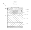
- FIG. 9 shows an example of a conventional vertical insulated-gate semiconductor device having a trench structure.
- the semiconductor device 9 A shown in the figure includes a first n-type semiconductor layer 911 , a second n-type semiconductor layer 912 , a p-type semiconductor layer 913 , an n-type semiconductor region 914 , a trench 93 , a gate electrode 94 and a gate insulating layer 95 .
- the first n-type semiconductor layer 911 serves as a base of the semiconductor device 9 A.
- the second n-type semiconductor layer 912 , the p-type semiconductor layer 913 , and the n-type semiconductor region 914 are stacked on the first n-type semiconductor layer 911 .
- the trench 93 is formed so as to penetrate through the p-type semiconductor layer 913 and the n-type semiconductor region 914 to reach the second n-type semiconductor layer 912 .
- the gate electrode 94 and the gate insulating layer 95 are provided inside the trench 93 .
- the gate insulating layer 95 insulates the gate electrode 94 from the second n-type semiconductor layer 912 , the p-type semiconductor layer 913 and the n-type semiconductor region 914 .
- the gate insulating layer 95 is formed along the inner surface of the trench 93 .
- the p-type semiconductor layer 913 includes a channel region.
- the channel region is along the trench 93 and in contact with the second n-type semiconductor layer 912 and the n-type semiconductor region 914 .
- the on-resistance is low from the viewpoint of reducing energy loss.
- the dielectric withstand voltage is high.
- the present invention has been proposed under the foregoing circumstances. It is an object of the present invention to provide a semiconductor device that allows reducing the on-resistance, increasing the dielectric withstand voltage and reducing the threshold voltage.
- a semiconductor device provided according to the present invention includes a first semiconductor layer having a first conductivity type, a second semiconductor layer provided on the first semiconductor layer and having a second conductivity type opposite to the first conductivity type, a trench penetrating through the second semiconductor layer to reach the first semiconductor layer, an insulating layer formed at a bottom and a side of the trench along an inner surface of the trench, a gate electrode which is insulated by the insulating layer from the first semiconductor layer and the second semiconductor layer and at least part of which is formed inside the trench, and a semiconductor region having the first conductivity type and formed around the trench on the second semiconductor layer.
- the second semiconductor layer includes a channel region that is along the trench and in contact with the first semiconductor layer and the semiconductor region.
- the size of the channel region in a depth direction of the trench is 0.1 to 0.5 ⁇ m, and the peak impurity concentration of the channel region is in a range of 4 ⁇ 10 17 cm ⁇ 3 to 2 ⁇ 10 18 cm ⁇ 3 .
- the channel region includes a high-concentration region where impurity concentration is equal to or higher than 5 ⁇ 10 17 cm ⁇ 3 .
- the high-concentration region is in the form of a layer that is in contact with the trench and that spreads in a direction perpendicular to the depth direction.
- the second semiconductor layer and the semiconductor region are made of silicon carbide.
- FIG. 1 is a sectional view showing a principal portion of a semiconductor device according to a first embodiment of the present invention
- FIG. 2 is a diagram showing the distribution of impurity concentration in a depth direction, in a p-type semiconductor region of the semiconductor device shown in FIG. 1 ;
- FIG. 3 is a sectional view showing a part of a manufacturing process of the semiconductor device shown in FIG. 1 ;
- FIG. 4 is a sectional view showing a step of the manufacturing process following the step shown in FIG. 2 ;
- FIG. 5 is a graph showing a threshold voltage with respect to p-type semiconductor layer highest concentration in the conventional semiconductor device
- FIG. 6A is a graph showing the relationship of a threshold voltage and a dielectric breakdown field to a p-type semiconductor layer highest concentration in the embodiment
- FIG. 6B is a graph showing the relationship of a channel resistance and a dielectric breakdown field to a p-type semiconductor layer highest concentration in the embodiment
- FIG. 7 is a sectional view showing a principal portion of a semiconductor device according to a second embodiment of the present invention.
- FIG. 8 is a sectional view showing a principal portion of a semiconductor device according to a third embodiment of the present invention.
- FIG. 9 is a sectional view showing a principal portion of a conventional semiconductor device.
- FIG. 1 depicts a semiconductor device according to a first embodiment of the present invention.
- the semiconductor device A 1 includes a first n-type semiconductor layer 11 , a second n-type semiconductor layer 12 , a p-type semiconductor layer 13 , a high-concentration p-type semiconductor region 13 a , an n-type semiconductor region 14 , a trench 3 , a gate electrode 41 , a gate insulating layer 5 , a source electrode 42 , a drain electrode 43 and an interlayer insulating film 6 , and has what is known as trench MOSFET structure.
- the first n-type semiconductor layer 11 is a substrate made of silicon carbide with high-concentration impurity added thereto, and serves as a base of the semiconductor device A 1 .
- the size of the first n-type semiconductor layer 11 in the depth direction x is approximately 300 ⁇ m.
- the impurity concentration in the first n-type semiconductor layer 11 is approximately 1 ⁇ 10 19 cm ⁇ 3 .
- the second n-type semiconductor layer 12 is formed on the first n-type semiconductor layer 11 .
- the second n-type semiconductor layer 12 is made of silicon carbide with low-concentration impurity added thereto.
- the size of the second n-type semiconductor layer 12 in the depth direction x is approximately 10 ⁇ m.
- the impurity concentration of the second n-type semiconductor layer 12 is approximately 6 ⁇ 10 15 cm ⁇ 3 .
- the impurity concentration of the second n-type semiconductor layer 12 is not limited to this and may be in a range of approximately 1 ⁇ 10 15 to 2 ⁇ 10 16 cm ⁇ 3 .
- the p-type semiconductor layer 13 is formed on the second n-type semiconductor layer 12 .
- the size of the p-type semiconductor layer 13 in the depth direction x is approximately 0.3 ⁇ m. It is preferable that the size of the p-type semiconductor layer 13 in the depth direction is in a range of 0.1 to 0.5 ⁇ m.
- the impurity concentration of the p-type semiconductor layer 13 is 1 ⁇ 10 17 cm ⁇ 3 or higher.
- the p-type semiconductor layer 13 includes a channel region.
- the channel region is along the trench 3 and in contact with the second n-type semiconductor layer 12 and the n-type semiconductor region 14 .
- the size of the p-type semiconductor layer 13 in the depth direction x needs to be in a range that provides a short channel effect.
- the short channel effect refers to the phenomenon that a decrease in size of the channel region in the depth direction x leads to a lower threshold voltage of the semiconductor device A 1 .
- the channel region may often fail to effectively perform its function.
- FIG. 2 shows the distribution of impurity concentration Ic in the depth direction x, in the p-type semiconductor layer 13 .
- the impurity concentration Ic With an increase in depth Dp, the impurity concentration Ic becomes higher.
- the impurity concentration Ic is highest at a certain depth Dp, and becomes lower with a further increase in depth Dp. Specifically, the impurity concentration Ic is highest at the depth Dp of approximately 0.5 ⁇ m, and the value at this point is approximately 1 ⁇ 10 18 cm ⁇ 3 .
- the p-type semiconductor layer 13 includes a high-concentration region 13 ′. In the figure, the portion where the impurity concentration is 5 ⁇ 10 17 cm ⁇ 3 or higher is the high-concentration region 13 ′.
- the size of the p-type semiconductor layer 13 exceeds 0.5 ⁇ m, it is difficult to create such impurity concentration distribution by e.g. impurity ion irradiation and to sufficiently exhibit the short channel effect.
- the n-type semiconductor region 14 is formed on the p-type semiconductor layer 13 .
- the size of the n-type semiconductor region 14 in the depth direction x is approximately 0.3 ⁇ m.
- the impurity concentration of the n-type semiconductor region 14 is approximately 1 ⁇ 10 20 cm ⁇ 3 .
- the impurity concentration of the n-type semiconductor region 14 is not limited to this, and it is only required that the impurity concentration is not lower than 1 ⁇ 10 18 cm ⁇ 3 .
- the high-concentration p-type semiconductor region 13 a is formed on the p-type semiconductor layer 13 .
- the trench 3 is formed so as to penetrate through the p-type semiconductor layer 13 and the n-type semiconductor region 14 to reach the second n-type semiconductor layer 12 .
- the size of the trench 3 in the depth direction x is equal to or greater than that of the p-type semiconductor layer 13 in the depth direction x. In this embodiment, the size of the trench 3 in the depth direction x is approximately 1 ⁇ m.
- the gate insulating layer 5 serves to insulate the gate electrode 41 from the second n-type semiconductor layer 12 , the p-type semiconductor layer 13 , and the n-type semiconductor region 14 .
- the gate insulating layer 5 is formed on the inner surface of the trench 3 at the bottom and sides of the trench 3 .
- the gate insulating layer 5 is made of, for example, silicon dioxide.
- the size of the side portion of the gate insulating layer 5 in the width direction y is approximately 0.1 ⁇ m.
- the size of the bottom portion of the gate insulating layer 5 in the direction x is approximately 0.08 ⁇ m.
- the source electrode 42 is made of aluminum for example, and in contact with the n-type semiconductor region 14 and the high-concentration p-type semiconductor region 13 a .
- the drain electrode 43 is made of aluminum for example, and in contact with the first n-type semiconductor layer 11 .
- the drain electrode 43 is formed on the opposite side of the second n-type semiconductor layer 12 across the first n-type semiconductor layer 11 .
- the interlayer insulating film 6 is formed so as to cover the gate electrode 41 .
- a semiconductor substrate made of silicon carbide, which is to become the first n-type semiconductor layer 11 is prepared.
- the second n-type semiconductor layer 12 is formed on the obverse surface of the substrate by epitaxial crystal growth.
- impurity ions p-type
- impurity ions implanted in the silicon carbide barely diffuses in the silicon carbide substrate.
- the location of the implanted impurity ion in the silicon carbide substrate in the depth direction exclusively depends on the irradiation energy.
- the impurity concentration distribution in the depth direction as that shown in FIG. 2 is provided. Then the n-type semiconductor region 14 and the high-concentration p-type semiconductor region 13 a are formed, for example by implanting impurity ions (n-type or p-type).
- the trench 3 , the gate insulating layer 5 and the gate electrode 41 are formed. Thereafter, the interlayer insulating film 6 , the source electrode 42 and the drain electrode 43 are formed. Through the foregoing process, the semiconductor device A 1 shown in FIG. 1 is obtained.
- FIG. 5 shows the relationship between peak concentration of impurity in the p-type semiconductor layer (p-type semiconductor layer highest concentration Ch) and threshold voltage Vt in the conventional semiconductor device.
- the short channel effect is not provided and the threshold voltage is not affected by the size of the channel region in the depth direction x, which is the difference from the semiconductor device A 1 .
- FIG. 6A shows the relationship of threshold voltage Vt and dielectric breakdown field Vb to p-type semiconductor layer highest concentration Ch in the semiconductor device A 1 according to this embodiment.
- FIG. 6B shows the relationship of channel resistance Rc and dielectric breakdown field Vb to p-type semiconductor layer highest concentration Ch in the semiconductor device A 1 according to this embodiment.
- the threshold voltage Vt is 9 V.
- the channel resistance is 3.8 m ⁇ cm 2 provided that the channel length is 1 ⁇ m and the dielectric breakdown field Vb at a corner portion of the trench 93 is 1.5 MVcm ⁇ 1 .
- the threshold voltage Vt is 13 V.
- the channel resistance is 5.9 m ⁇ cm 2 under a condition similar to the above, i.e. provided that the channel length is 1 ⁇ m and the dielectric breakdown field Vb at the bottom portion of the trench 93 is 1.5 MVcm ⁇ 1 .
- the threshold voltage Vt is in a range of 4 V to 11 V when the p-type semiconductor layer highest concentration Ch is in a range of 4 ⁇ 10 17 cm ⁇ 3 to 2 ⁇ 10 18 cm ⁇ 3 .
- the dielectric breakdown field Vb is in a range of 0.9 MVcm ⁇ 1 to 1.7 MVcm ⁇ 1 .
- the channel resistance Rc is in a range of 0.5 m ⁇ cm 2 to 2.9 m ⁇ cm 2 .
- the values of threshold voltage Vt, dielectric breakdown field Vb and channel resistance Rc at several points in the above-described range of p-type semiconductor layer highest concentration Ch will be cited.
- the threshold voltage Vt is 4 V.
- the dielectric breakdown field Vb is approximately 0.9 MVcm ⁇ 1
- the channel resistance Rc is 0.5 m ⁇ cm 2 .
- the threshold voltage Vt is 11 V.
- the dielectric breakdown field Vb is approximately 1.7 MVcm ⁇ 1
- the channel resistance Rc is 2.9 m ⁇ cm 2 .
- the threshold voltage Vt is 7 V.
- the dielectric breakdown field Vb is approximately 1.5 MVcm ⁇ 1
- the channel resistance Rc is 1 m ⁇ cm 2 .
- threshold voltage Vt is maintained at a relatively low level. Presumably, this is because the short channel effect takes place despite that the impurity concentration in the p-type semiconductor layer 13 is set in the foregoing range.
- the dielectric breakdown field Vb is maintained at a relatively high level. This can be construed as a result of the impurity concentration of the p-type semiconductor layer 13 remaining high.
- the channel resistance Rc is relatively small. This can be construed as a result of the reduction in size of the channel region in the depth direction.
- the values of threshold voltage Vt, dielectric breakdown field Vb and channel resistance Rc of the semiconductor device A 1 are in a desirable range as a whole. Consequently, the semiconductor device A 1 allows achieving more desirable values of on-resistance, dielectric withstand voltage and threshold voltage than those of the conventional semiconductor device.
- FIGS. 7 and 8 each depict another example of the semiconductor device according to the present invention.
- constituents similar to those of the foregoing embodiment are given the same reference signs, and the description thereof is appropriately omitted.
- FIG. 7 shows a semiconductor device according to a second embodiment of the present invention.
- the semiconductor device A 2 according to this embodiment is different from the semiconductor device A 1 in having a structure of what is known as an IGBT (Insulated Gate Bipolar Transistor).
- the semiconductor device A 2 is similar to the semiconductor device A 1 in the size of the channel region and impurity concentration, as well as in including the high-concentration region 13 ′ shown in FIG. 2 and being made of silicon carbide.
- a p-type substrate 15 is provided on the back surface of the n-type semiconductor layer 12 .
- a nickel layer is provided between the p-type substrate 15 and the drain electrode 43 .
- This structure also allows, as does the semiconductor device A 1 , achieving relatively desirable values of on-resistance, dielectric withstand voltage and threshold voltage. Further, the semiconductor device A 2 as an IGBT is advantageous for reducing the resistance, and hence more suitable for use under a high voltage than the semiconductor device A 1 .
- FIG. 8 shows the semiconductor device according to a third embodiment of the present invention.
- the semiconductor device A 3 according to this embodiment is different from the semiconductor device A 1 in having a structure of what is known as an SJ (Super Junction) MOSFET.
- the semiconductor device A 2 is similar to the semiconductor device A 1 in the size of the channel region and impurity concentration, as well as in including the high-concentration region 13 ′ shown in FIG. 2 and being made of silicon carbide.
- a p-type semiconductor layer 17 is formed to sandwich the n-type semiconductor layer 12 in the direction y.
- the p-type semiconductor layer 17 has generally the same thickness as the second n-type semiconductor layer 12 , and is in contact with the first n-type semiconductor layer 11 and the p-type semiconductor layer 13 .
- a nickel layer 16 is provided between the first n-type semiconductor layer 11 and the drain electrode 43 .
- the structure is not limited to this, and the p-type semiconductor layer 17 may be formed along only halfway of the second n-type semiconductor layer 12 from the p-type semiconductor layer 13 .
- the first n-type semiconductor layer 11 serves as what is known as a drift layer
- the p-type semiconductor layer 17 as a RESURF layer.
- Such structure also allows, as does the semiconductor device A 1 , achieving relatively desirable values of on-resistance, dielectric withstand voltage and threshold voltage. Further, the semiconductor device A 3 as an SJMOSFET is advantageous for achieving both of a higher withstand voltage and a lower resistance.
- the semiconductor device according to the present invention is in no way limited to the foregoing embodiments. Specific structure of the constituents of the semiconductor device according to the present invention may be varied in design in various manners.
Abstract
A semiconductor device (A1) includes a first n-type semiconductor layer (11), a second n-type semiconductor layer (12), a p-type semiconductor layer (13), a trench (3), an insulating layer (5), a gate electrode (41), and an n-type semiconductor region (14). The p-type semiconductor layer (13) includes a channel region that is along the trench (3) and in contact with the second n-type semiconductor layer (12) and the n-type semiconductor region (14). The size of the channel region in the depth direction x is 0.1 to 0.5 μm. The channel region includes a high-concentration region where the peak impurity concentration is approximately 1×1018 cm−3. The semiconductor device A1 thus configured allows achieving desirable values of on-resistance, dielectric withstand voltage and threshold voltage.
Description
This application is a Continuation of U.S. Ser. No. 12/993,209, filed Nov. 17, 2010, which is a National Stage Application of PCT/JP2009/059257, filed May 20, 2009 and issued as U.S. Pat. No. 8,575,622, which applications are incorporated herein by reference.
The present invention relates to a semiconductor device having a trench structure.
The first n-type semiconductor layer 911 serves as a base of the semiconductor device 9A. The second n-type semiconductor layer 912, the p-type semiconductor layer 913, and the n-type semiconductor region 914 are stacked on the first n-type semiconductor layer 911.
The trench 93 is formed so as to penetrate through the p-type semiconductor layer 913 and the n-type semiconductor region 914 to reach the second n-type semiconductor layer 912. Inside the trench 93, the gate electrode 94 and the gate insulating layer 95 are provided. The gate insulating layer 95 insulates the gate electrode 94 from the second n-type semiconductor layer 912, the p-type semiconductor layer 913 and the n-type semiconductor region 914. The gate insulating layer 95 is formed along the inner surface of the trench 93.
The p-type semiconductor layer 913 includes a channel region. The channel region is along the trench 93 and in contact with the second n-type semiconductor layer 912 and the n-type semiconductor region 914.
Regarding the semiconductor device 9A thus configured, it is preferable that the on-resistance is low from the viewpoint of reducing energy loss. To prevent dielectric breakdown, it is preferable that the dielectric withstand voltage is high. Also, there is a demand for a reduced threshold voltage so that the semiconductor device can be driven by applying a relatively low voltage to the gate electrode (see Patent Document 1, for example).
- Patent Document 1: JP-A-2006-32420
The present invention has been proposed under the foregoing circumstances. It is an object of the present invention to provide a semiconductor device that allows reducing the on-resistance, increasing the dielectric withstand voltage and reducing the threshold voltage.
A semiconductor device provided according to the present invention includes a first semiconductor layer having a first conductivity type, a second semiconductor layer provided on the first semiconductor layer and having a second conductivity type opposite to the first conductivity type, a trench penetrating through the second semiconductor layer to reach the first semiconductor layer, an insulating layer formed at a bottom and a side of the trench along an inner surface of the trench, a gate electrode which is insulated by the insulating layer from the first semiconductor layer and the second semiconductor layer and at least part of which is formed inside the trench, and a semiconductor region having the first conductivity type and formed around the trench on the second semiconductor layer. The second semiconductor layer includes a channel region that is along the trench and in contact with the first semiconductor layer and the semiconductor region. The size of the channel region in a depth direction of the trench is 0.1 to 0.5 μm, and the peak impurity concentration of the channel region is in a range of 4×1017 cm−3 to 2×1018 cm−3.
In a preferred embodiment of the present invention, the channel region includes a high-concentration region where impurity concentration is equal to or higher than 5×1017 cm−3. The high-concentration region is in the form of a layer that is in contact with the trench and that spreads in a direction perpendicular to the depth direction.
In a preferred embodiment of the present invention, the second semiconductor layer and the semiconductor region are made of silicon carbide.
Other features and advantages of the present invention will become more apparent from detailed description given below with reference to the accompanying drawings.
Preferred embodiments of the present invention are described below with reference to the accompanying drawings.
The first n-type semiconductor layer 11 is a substrate made of silicon carbide with high-concentration impurity added thereto, and serves as a base of the semiconductor device A1. The size of the first n-type semiconductor layer 11 in the depth direction x is approximately 300 μm. The impurity concentration in the first n-type semiconductor layer 11 is approximately 1×1019 cm−3.
The second n-type semiconductor layer 12 is formed on the first n-type semiconductor layer 11. The second n-type semiconductor layer 12 is made of silicon carbide with low-concentration impurity added thereto. The size of the second n-type semiconductor layer 12 in the depth direction x is approximately 10 μm. The impurity concentration of the second n-type semiconductor layer 12 is approximately 6×1015 cm−3. However, the impurity concentration of the second n-type semiconductor layer 12 is not limited to this and may be in a range of approximately 1×10¹⁵ to 2×1016 cm−3.
The p-type semiconductor layer 13 is formed on the second n-type semiconductor layer 12. The size of the p-type semiconductor layer 13 in the depth direction x is approximately 0.3 μm. It is preferable that the size of the p-type semiconductor layer 13 in the depth direction is in a range of 0.1 to 0.5 μm. The impurity concentration of the p-type semiconductor layer 13 is 1×1017 cm−3 or higher.
The p-type semiconductor layer 13 includes a channel region. The channel region is along the trench 3 and in contact with the second n-type semiconductor layer 12 and the n-type semiconductor region 14. The size of the p-type semiconductor layer 13 in the depth direction x needs to be in a range that provides a short channel effect. The short channel effect refers to the phenomenon that a decrease in size of the channel region in the depth direction x leads to a lower threshold voltage of the semiconductor device A1. When the size of the p-type semiconductor layer 13 in the depth direction is smaller than 0.1 μm, the channel region may often fail to effectively perform its function.
The n-type semiconductor region 14 is formed on the p-type semiconductor layer 13. The size of the n-type semiconductor region 14 in the depth direction x is approximately 0.3 μm. The impurity concentration of the n-type semiconductor region 14 is approximately 1×1020 cm−3. However, the impurity concentration of the n-type semiconductor region 14 is not limited to this, and it is only required that the impurity concentration is not lower than 1×1018 cm−3. The high-concentration p-type semiconductor region 13 a is formed on the p-type semiconductor layer 13.
The trench 3 is formed so as to penetrate through the p-type semiconductor layer 13 and the n-type semiconductor region 14 to reach the second n-type semiconductor layer 12. The size of the trench 3 in the depth direction x is equal to or greater than that of the p-type semiconductor layer 13 in the depth direction x. In this embodiment, the size of the trench 3 in the depth direction x is approximately 1 μm.
Inside the trench 3, the gate electrode 41 and the gate insulating layer 5 are formed. The gate insulating layer 5 serves to insulate the gate electrode 41 from the second n-type semiconductor layer 12, the p-type semiconductor layer 13, and the n-type semiconductor region 14. The gate insulating layer 5 is formed on the inner surface of the trench 3 at the bottom and sides of the trench 3. In this embodiment, the gate insulating layer 5 is made of, for example, silicon dioxide.
The size of the side portion of the gate insulating layer 5 in the width direction y is approximately 0.1 μm. The size of the bottom portion of the gate insulating layer 5 in the direction x is approximately 0.08 μm.
The source electrode 42 is made of aluminum for example, and in contact with the n-type semiconductor region 14 and the high-concentration p-type semiconductor region 13 a. The drain electrode 43 is made of aluminum for example, and in contact with the first n-type semiconductor layer 11. The drain electrode 43 is formed on the opposite side of the second n-type semiconductor layer 12 across the first n-type semiconductor layer 11. The interlayer insulating film 6 is formed so as to cover the gate electrode 41.
An example of a manufacturing method of the semiconductor device A1 is described below with reference to FIGS. 3 and 4 .
First, as shown in FIG. 3 , a semiconductor substrate made of silicon carbide, which is to become the first n-type semiconductor layer 11, is prepared. Then, the second n-type semiconductor layer 12 is formed on the obverse surface of the substrate by epitaxial crystal growth. Then, impurity ions (p-type) such as aluminum ion or boron ion are implanted into the upper surface of the second n-type semiconductor layer 12 to thereby form the p-type semiconductor layer 13. The impurity ions implanted in the silicon carbide barely diffuses in the silicon carbide substrate. The location of the implanted impurity ion in the silicon carbide substrate in the depth direction exclusively depends on the irradiation energy. Accordingly, by adjusting the energy when implanting impurity ions, the impurity concentration distribution in the depth direction as that shown in FIG. 2 is provided. Then the n-type semiconductor region 14 and the high-concentration p-type semiconductor region 13 a are formed, for example by implanting impurity ions (n-type or p-type).
Then, as shown in FIG. 4 , the trench 3, the gate insulating layer 5 and the gate electrode 41 are formed. Thereafter, the interlayer insulating film 6, the source electrode 42 and the drain electrode 43 are formed. Through the foregoing process, the semiconductor device A1 shown in FIG. 1 is obtained.
A comparison is made below between the semiconductor device A1 according to the present invention and the conventional semiconductor device.
According to FIG. 5 , in the conventional semiconductor device 9A, when the highest impurity concentration Ch in the p-type semiconductor layer 913 is 2×1017 cm−3, the threshold voltage Vt is 9 V. In this state, the channel resistance is 3.8 mΩcm2 provided that the channel length is 1 μm and the dielectric breakdown field Vb at a corner portion of the trench 93 is 1.5 MVcm−1. When the highest impurity concentration Ch in the p-type semiconductor layer 913 is 5×1017 cm−3, the threshold voltage Vt is 13 V. In this state, the channel resistance is 5.9 mΩcm2 under a condition similar to the above, i.e. provided that the channel length is 1 μm and the dielectric breakdown field Vb at the bottom portion of the trench 93 is 1.5 MVcm−1.
In contrast, according to FIG. 6A , the threshold voltage Vt is in a range of 4 V to 11 V when the p-type semiconductor layer highest concentration Ch is in a range of 4×1017 cm−3 to 2×1018 cm−3. In this range of p-type semiconductor layer highest concentration Ch, the dielectric breakdown field Vb is in a range of 0.9 MVcm−1 to 1.7 MVcm−1. According to FIG. 6B , in this range of p-type semiconductor layer highest concentration Ch, the channel resistance Rc is in a range of 0.5 mΩcm2 to 2.9 mΩcm2.
Here, the values of threshold voltage Vt, dielectric breakdown field Vb and channel resistance Rc at several points in the above-described range of p-type semiconductor layer highest concentration Ch will be cited. According to FIGS. 6A and 6B , when the p-type semiconductor layer highest concentration Ch is 4×1017 cm−3, the threshold voltage Vt is 4 V. In this state, the dielectric breakdown field Vb is approximately 0.9 MVcm−1, while the channel resistance Rc is 0.5 mΩcm2. When the p-type semiconductor layer highest concentration Ch is 2×1018 cm−3, the threshold voltage Vt is 11 V. In this state, the dielectric breakdown field Vb is approximately 1.7 MVcm−1, and the channel resistance Rc is 2.9 mΩcm2. When the p-type semiconductor layer highest concentration Ch is 1×1018 cm−3, which is within the range of 4×1017 cm−3 to 2×1018 cm−3, the threshold voltage Vt is 7 V. In this state, the dielectric breakdown field Vb is approximately 1.5 MVcm−1, and the channel resistance Rc is 1 mΩcm2.
The foregoing values of threshold voltage Vt, dielectric breakdown field Vb and channel resistance Rc are compared with those of the conventional semiconductor device described above with reference to FIG. 5 . In the semiconductor device A1, the threshold voltage Vt is maintained at a relatively low level. Presumably, this is because the short channel effect takes place despite that the impurity concentration in the p-type semiconductor layer 13 is set in the foregoing range. Also, the dielectric breakdown field Vb is maintained at a relatively high level. This can be construed as a result of the impurity concentration of the p-type semiconductor layer 13 remaining high. Further, the channel resistance Rc is relatively small. This can be construed as a result of the reduction in size of the channel region in the depth direction. In this way, the values of threshold voltage Vt, dielectric breakdown field Vb and channel resistance Rc of the semiconductor device A1 are in a desirable range as a whole. Consequently, the semiconductor device A1 allows achieving more desirable values of on-resistance, dielectric withstand voltage and threshold voltage than those of the conventional semiconductor device.
This structure also allows, as does the semiconductor device A1, achieving relatively desirable values of on-resistance, dielectric withstand voltage and threshold voltage. Further, the semiconductor device A2 as an IGBT is advantageous for reducing the resistance, and hence more suitable for use under a high voltage than the semiconductor device A1.
In this embodiment, a p-type semiconductor layer 17 is formed to sandwich the n-type semiconductor layer 12 in the direction y. The p-type semiconductor layer 17 has generally the same thickness as the second n-type semiconductor layer 12, and is in contact with the first n-type semiconductor layer 11 and the p-type semiconductor layer 13. Between the first n-type semiconductor layer 11 and the drain electrode 43, a nickel layer 16 is provided. However, the structure is not limited to this, and the p-type semiconductor layer 17 may be formed along only halfway of the second n-type semiconductor layer 12 from the p-type semiconductor layer 13. In the semiconductor device A3 of the SJMOSFET structure, the first n-type semiconductor layer 11 serves as what is known as a drift layer, and the p-type semiconductor layer 17 as a RESURF layer.
Such structure also allows, as does the semiconductor device A1, achieving relatively desirable values of on-resistance, dielectric withstand voltage and threshold voltage. Further, the semiconductor device A3 as an SJMOSFET is advantageous for achieving both of a higher withstand voltage and a lower resistance.
The semiconductor device according to the present invention is in no way limited to the foregoing embodiments. Specific structure of the constituents of the semiconductor device according to the present invention may be varied in design in various manners.
Claims (20)
1. A semiconductor device comprising:
a first semiconductor layer having a first conductivity type and made of silicon carbide;
a second semiconductor layer made of silicon carbide, provided on the first semiconductor layer and having a second conductivity type opposite to the first conductivity type;
a trench penetrating through the second semiconductor layer to reach the first semiconductor layer;
an insulating layer formed at a bottom and a side of the trench along an inner surface of the trench;
a gate electrode insulated by the insulating layer from the first semiconductor layer and the second semiconductor layer, at least part of the gate electrode being formed inside the trench; and
a semiconductor region made of silicon carbide, having the first conductivity type and formed around the trench on the second semiconductor layer;
wherein the second semiconductor layer includes a region that is along the trench,
the region of the second semiconductor layer that is along the trench includes a high-concentration region where impurity concentration is equal to or higher than 5×1017 cm−3,
the high-concentration region is in a form of a layer that is in contact with the trench and that spreads in a direction perpendicular to a depth direction of the trench, and
the high-concentration region has a peak impurity region in a medium portion of the second semiconductor layer along the trench.
2. The semiconductor device according to claim 1 , wherein a size of the second semiconductor layer in the depth direction of the trench is 0.1 to 0.5 μm, and
a peak impurity concentration of the region of the second semiconductor layer that is along the trench is in a range of 7×1017 cm−3 to 1.5×1018 cm−3.
3. The semiconductor device according to claim 1 , wherein the insulating layer includes a bottom portion and a side portion that are different in thickness from each other.
4. The semiconductor device according to claim 3 , wherein the side portion of the insulating layer is thicker than the bottom portion of the insulating layer.
5. The semiconductor device according to claim 1 , wherein an impurity concentration of the first semiconductor layer is in a range of 1×1015 cm−3 to 2×1016 cm−3.
6. The semiconductor device according to claim 1 , wherein an impurity concentration of the second semiconductor layer is not less than 1×1017 cm−3.
7. The semiconductor device according to claim 1 , wherein an impurity concentration of the semiconductor region is not less than 1×1018 cm−3.
8. The semiconductor device according to claim 1 , wherein an impurity concentration of the second semiconductor layer initially increases, reaches a maximum at a predetermined depth and decreases, as proceeding from the semiconductor region toward the first semiconductor layer in the depth direction of the trench.
9. The semiconductor device according to claim 8 , wherein a size of the second semiconductor layer in the depth direction of the trench is 0.1 to 0.5 μm, and
a peak impurity concentration of the region of the second semiconductor layer that is along the trench is in a range of 7×1017 cm−3 to 1.5×1018 cm−3.
10. The semiconductor device according to claim 8 , wherein the insulating layer includes a bottom portion and a side portion that are different in thickness from each other.
11. The semiconductor device according to claim 8 , wherein an impurity concentration of the first semiconductor layer is in a range of 1×1015 cm−3 to 2×1016 cm−3.
12. The semiconductor device according to claim 8 , wherein an impurity concentration of the semiconductor region is not less than 1×1018 cm−3.
13. The semiconductor device according to claim 8 , wherein a position of the predetermined depth is closer to the first semiconductor layer than to the semiconductor region in the depth direction of the trench.
14. The semiconductor device according to claim 13 , wherein a size of the second semiconductor layer in the depth direction of the trench is 0.1 to 0.5 μm, and
a peak impurity concentration of the region of the second semiconductor layer that is along the trench is in a range of 7×1017 cm−3 to 1.5×1018 cm−3.
15. The semiconductor device according to claim 13 , wherein the insulating layer includes a bottom portion and a side portion that are different in thickness from each other.
16. The semiconductor device according to claim 13 , wherein an impurity concentration of the first semiconductor layer is in a range of 1×1015 cm−3 to 2×1016 cm−3.
17. The semiconductor device according to claim 13 , wherein an impurity concentration of the semiconductor region is not less than 1×1018 cm−3.
18. The semiconductor device according to claim 1 , configured as an insulated gate bipolar transistor.
19. The semiconductor device according to claim 1 , configured as a super junction MOSFET.
20. The semiconductor device according to claim 1 , wherein when a highest impurity concentration of the second semiconductor layer is in a range of 4×1017 cm−3 to 2×1018 cm−3, the semiconductor device has a threshold voltage in a range of 4 V to 11 V, a dielectric breakdown field in a range of 0.9 MVcm−1 to 1.7 MVcm−1, and a channel resistance in a range of 0.5 mΩcm2 to 2.9 mΩcm2.
Priority Applications (1)
| Application Number | Priority Date | Filing Date | Title |
|---|---|---|---|
| US14/049,810 US9024329B2 (en) | 2008-05-20 | 2013-10-09 | Silicon carbide trench MOSFET having reduced on-resistance, increased dielectric withstand voltage, and reduced threshold voltage |
Applications Claiming Priority (5)
| Application Number | Priority Date | Filing Date | Title |
|---|---|---|---|
| JP2008-131884 | 2008-05-20 | ||
| JP2008131884 | 2008-05-20 | ||
| PCT/JP2009/059257 WO2009142233A1 (en) | 2008-05-20 | 2009-05-20 | Semiconductor device |
| US99320910A | 2010-11-17 | 2010-11-17 | |
| US14/049,810 US9024329B2 (en) | 2008-05-20 | 2013-10-09 | Silicon carbide trench MOSFET having reduced on-resistance, increased dielectric withstand voltage, and reduced threshold voltage |
Related Parent Applications (2)
| Application Number | Title | Priority Date | Filing Date |
|---|---|---|---|
| US12/993,209 Continuation US8575622B2 (en) | 2008-05-20 | 2009-05-20 | Silicon carbide trench MOSFET having reduced on-resistance, increased dielectric withstand voltage, and reduced threshold voltage |
| PCT/JP2009/059257 Continuation WO2009142233A1 (en) | 2008-05-20 | 2009-05-20 | Semiconductor device |
Publications (2)
| Publication Number | Publication Date |
|---|---|
| US20140034969A1 US20140034969A1 (en) | 2014-02-06 |
| US9024329B2 true US9024329B2 (en) | 2015-05-05 |
Family
ID=41340161
Family Applications (2)
| Application Number | Title | Priority Date | Filing Date |
|---|---|---|---|
| US12/993,209 Active 2030-01-28 US8575622B2 (en) | 2008-05-20 | 2009-05-20 | Silicon carbide trench MOSFET having reduced on-resistance, increased dielectric withstand voltage, and reduced threshold voltage |
| US14/049,810 Active US9024329B2 (en) | 2008-05-20 | 2013-10-09 | Silicon carbide trench MOSFET having reduced on-resistance, increased dielectric withstand voltage, and reduced threshold voltage |
Family Applications Before (1)
| Application Number | Title | Priority Date | Filing Date |
|---|---|---|---|
| US12/993,209 Active 2030-01-28 US8575622B2 (en) | 2008-05-20 | 2009-05-20 | Silicon carbide trench MOSFET having reduced on-resistance, increased dielectric withstand voltage, and reduced threshold voltage |
Country Status (5)
| Country | Link |
|---|---|
| US (2) | US8575622B2 (en) |
| EP (3) | EP2293336B1 (en) |
| JP (2) | JP5819064B2 (en) |
| CN (1) | CN102037564B (en) |
| WO (1) | WO2009142233A1 (en) |
Families Citing this family (18)
| Publication number | Priority date | Publication date | Assignee | Title |
|---|---|---|---|---|
| JP2012099601A (en) | 2010-11-01 | 2012-05-24 | Sumitomo Electric Ind Ltd | Semiconductor device and method of manufacturing the same |
| JP2012160584A (en) * | 2011-02-01 | 2012-08-23 | Sumitomo Electric Ind Ltd | Semiconductor device |
| JP5592997B2 (en) | 2011-05-30 | 2014-09-17 | パナソニック株式会社 | Semiconductor device and manufacturing method thereof |
| CN103378141B (en) * | 2012-04-25 | 2016-03-09 | 上海北车永电电子科技有限公司 | Insulated gate bipolar transistor and preparation method thereof |
| JP6056292B2 (en) | 2012-09-12 | 2017-01-11 | 住友電気工業株式会社 | Method for manufacturing silicon carbide semiconductor device |
| JP2014056913A (en) | 2012-09-12 | 2014-03-27 | Sumitomo Electric Ind Ltd | Silicon carbide semiconductor device |
| JP5811973B2 (en) | 2012-09-12 | 2015-11-11 | 住友電気工業株式会社 | Method for manufacturing silicon carbide semiconductor device |
| WO2014102916A1 (en) * | 2012-12-26 | 2014-07-03 | 株式会社日立製作所 | Silicon carbide semiconductor device |
| JP6048317B2 (en) * | 2013-06-05 | 2016-12-21 | 株式会社デンソー | Silicon carbide semiconductor device |
| JP2015072999A (en) * | 2013-10-02 | 2015-04-16 | 株式会社デンソー | Silicon carbide semiconductor device |
| JP6110900B2 (en) * | 2015-07-07 | 2017-04-05 | ルネサスエレクトロニクス株式会社 | Manufacturing method of semiconductor device |
| DE102016226237A1 (en) | 2016-02-01 | 2017-08-03 | Fuji Electric Co., Ltd. | SILICON CARBIDE SEMICONDUCTOR DEVICE AND METHOD FOR PRODUCING A SILICON CARBIDE SEMICONDUCTOR DEVICE |
| JP6115678B1 (en) * | 2016-02-01 | 2017-04-19 | 富士電機株式会社 | Silicon carbide semiconductor device and method for manufacturing silicon carbide semiconductor device |
| JP6907233B2 (en) | 2016-02-02 | 2021-07-21 | アーベーベー・シュバイツ・アーゲーABB Schweiz AG | Power semiconductor device |
| JP6784921B2 (en) * | 2017-02-17 | 2020-11-18 | 株式会社デンソー | Switching element and its manufacturing method |
| US10497777B2 (en) | 2017-09-08 | 2019-12-03 | Hestia Power Inc. | Semiconductor power device |
| DE102018200676A1 (en) * | 2018-01-17 | 2019-07-18 | Robert Bosch Gmbh | Power electronic component |
| JP2020123607A (en) * | 2019-01-29 | 2020-08-13 | トヨタ自動車株式会社 | Semiconductor device |
Citations (9)
| Publication number | Priority date | Publication date | Assignee | Title |
|---|---|---|---|---|
| US5742076A (en) | 1996-06-05 | 1998-04-21 | North Carolina State University | Silicon carbide switching devices having near ideal breakdown voltage capability and ultralow on-state resistance |
| JP2001250947A (en) | 2000-03-06 | 2001-09-14 | Toshiba Corp | Power semiconductor element and its manufacturing method |
| JP2003051598A (en) | 2001-05-31 | 2003-02-21 | Hideshi Ito | High-frequency power mosfet |
| JP2004335990A (en) | 2003-03-10 | 2004-11-25 | Fuji Electric Device Technology Co Ltd | Mis type semiconductor device |
| JP2005005655A (en) | 2002-06-28 | 2005-01-06 | Internatl Rectifier Corp | Mos gate semiconductor device |
| JP2006032420A (en) | 2004-07-12 | 2006-02-02 | Toyota Motor Corp | Insulation gate semiconductor device and manufacturing method thereof |
| US20060054970A1 (en) | 2004-09-08 | 2006-03-16 | Sanyo Electric Co., Ltd. | Semiconductor device and method of manufacturing the same |
| JP2007157751A (en) | 2005-11-30 | 2007-06-21 | Toyota Motor Corp | Silicon carbide semiconductor device and its fabrication process |
| JP2007281265A (en) | 2006-04-10 | 2007-10-25 | Mitsubishi Electric Corp | Trench mosfet, and its manufacturing method |
Family Cites Families (6)
| Publication number | Priority date | Publication date | Assignee | Title |
|---|---|---|---|---|
| JPH06101566B2 (en) * | 1984-04-25 | 1994-12-12 | 株式会社日立製作所 | Vertical field effect transistor |
| JPH11145457A (en) * | 1997-11-07 | 1999-05-28 | Nec Corp | Vertical field effect transistor |
| JP4696335B2 (en) * | 2000-05-30 | 2011-06-08 | 株式会社デンソー | Semiconductor device and manufacturing method thereof |
| JP4945055B2 (en) * | 2003-08-04 | 2012-06-06 | ルネサスエレクトロニクス株式会社 | Semiconductor device and manufacturing method thereof |
| JP3954541B2 (en) * | 2003-08-05 | 2007-08-08 | 株式会社東芝 | Semiconductor device and manufacturing method thereof |
| JP4744958B2 (en) * | 2005-07-13 | 2011-08-10 | 株式会社東芝 | Semiconductor device and manufacturing method thereof |
-
2009
- 2009-05-20 EP EP09750595.2A patent/EP2293336B1/en active Active
- 2009-05-20 CN CN2009801184067A patent/CN102037564B/en active Active
- 2009-05-20 US US12/993,209 patent/US8575622B2/en active Active
- 2009-05-20 EP EP19203089.8A patent/EP3614441B1/en active Active
- 2009-05-20 WO PCT/JP2009/059257 patent/WO2009142233A1/en active Application Filing
- 2009-05-20 JP JP2010513040A patent/JP5819064B2/en active Active
- 2009-05-20 EP EP22206776.1A patent/EP4156302A1/en active Pending
-
2013
- 2013-10-09 US US14/049,810 patent/US9024329B2/en active Active
-
2014
- 2014-08-07 JP JP2014161371A patent/JP2014241435A/en active Pending
Patent Citations (13)
| Publication number | Priority date | Publication date | Assignee | Title |
|---|---|---|---|---|
| US5742076A (en) | 1996-06-05 | 1998-04-21 | North Carolina State University | Silicon carbide switching devices having near ideal breakdown voltage capability and ultralow on-state resistance |
| JP2001250947A (en) | 2000-03-06 | 2001-09-14 | Toshiba Corp | Power semiconductor element and its manufacturing method |
| US6495871B2 (en) | 2000-03-06 | 2002-12-17 | Kabushiki Kaisha Toshiba | Power semiconductor element capable of improving short circuit withstand capability while maintaining low on-voltage and method of fabricating the same |
| JP2003051598A (en) | 2001-05-31 | 2003-02-21 | Hideshi Ito | High-frequency power mosfet |
| US6919599B2 (en) | 2002-06-28 | 2005-07-19 | International Rectifier Corporation | Short channel trench MOSFET with reduced gate charge |
| JP2005005655A (en) | 2002-06-28 | 2005-01-06 | Internatl Rectifier Corp | Mos gate semiconductor device |
| JP2004335990A (en) | 2003-03-10 | 2004-11-25 | Fuji Electric Device Technology Co Ltd | Mis type semiconductor device |
| US7692239B2 (en) | 2003-03-10 | 2010-04-06 | Fuji Electric Device Technology Co., Ltd. | MIS-type semiconductor device |
| JP2006032420A (en) | 2004-07-12 | 2006-02-02 | Toyota Motor Corp | Insulation gate semiconductor device and manufacturing method thereof |
| US20060054970A1 (en) | 2004-09-08 | 2006-03-16 | Sanyo Electric Co., Ltd. | Semiconductor device and method of manufacturing the same |
| JP2006080177A (en) | 2004-09-08 | 2006-03-23 | Sanyo Electric Co Ltd | Semiconductor apparatus and its manufacturing method |
| JP2007157751A (en) | 2005-11-30 | 2007-06-21 | Toyota Motor Corp | Silicon carbide semiconductor device and its fabrication process |
| JP2007281265A (en) | 2006-04-10 | 2007-10-25 | Mitsubishi Electric Corp | Trench mosfet, and its manufacturing method |
Non-Patent Citations (2)
| Title |
|---|
| Otake et al. "GaN-Based Trench Gate Metal Oxide Semiconductor Field Effect Transistors with Over 100 cm2/(Vs) Channel Mobility". Japanese Journal of Applied Physics, vol. 46, No. 25, pp. L599-L601 (2007). |
| Tsui et al. "Trench Gate Power MOSFETs with Retrograde Body Profile". Proceedings of 2004 International Symposium on Power Semiconductor Devices & IC's, Kitakyushu, p. 213-216 (2004). |
Also Published As
| Publication number | Publication date |
|---|---|
| EP3614441A1 (en) | 2020-02-26 |
| CN102037564B (en) | 2013-04-10 |
| JPWO2009142233A1 (en) | 2011-09-29 |
| EP4156302A1 (en) | 2023-03-29 |
| US8575622B2 (en) | 2013-11-05 |
| EP2293336B1 (en) | 2019-11-27 |
| CN102037564A (en) | 2011-04-27 |
| EP2293336A1 (en) | 2011-03-09 |
| JP5819064B2 (en) | 2015-11-18 |
| JP2014241435A (en) | 2014-12-25 |
| EP3614441B1 (en) | 2023-04-19 |
| EP2293336A4 (en) | 2014-01-29 |
| US20140034969A1 (en) | 2014-02-06 |
| WO2009142233A1 (en) | 2009-11-26 |
| US20110068353A1 (en) | 2011-03-24 |
Similar Documents
| Publication | Publication Date | Title |
|---|---|---|
| US9024329B2 (en) | Silicon carbide trench MOSFET having reduced on-resistance, increased dielectric withstand voltage, and reduced threshold voltage | |
| US8080858B2 (en) | Semiconductor component having a space saving edge structure | |
| US9601334B2 (en) | Semiconductor device and the method of manufacturing the same | |
| US10763351B2 (en) | Vertical trench DMOSFET having integrated implants forming enhancement diodes in parallel with the body diode | |
| US20210098568A1 (en) | Power semiconductor devices having gate trenches and buried edge terminations and related methods | |
| US7605423B2 (en) | Semiconductor device | |
| US7928505B2 (en) | Semiconductor device with vertical trench and lightly doped region | |
| US8174066B2 (en) | Semiconductor device and method of manufacturing semiconductor device | |
| JP5586887B2 (en) | Semiconductor device and manufacturing method thereof | |
| JP4813762B2 (en) | Semiconductor device and manufacturing method thereof | |
| JP2009289904A (en) | Semiconductor device | |
| US6919599B2 (en) | Short channel trench MOSFET with reduced gate charge | |
| US20110220991A1 (en) | Semiconductor device | |
| US9000478B2 (en) | Vertical IGBT adjacent a RESURF region | |
| US7701001B2 (en) | Short channel trench power MOSFET with low threshold voltage | |
| US20090206397A1 (en) | Lateral Trench MOSFET with Conformal Depletion-Assist Layer | |
| US20030006483A1 (en) | Short channel power MOSFET with increased breakdown voltage | |
| US6781203B2 (en) | MOSFET with reduced threshold voltage and on resistance and process for its manufacture | |
| WO2009060406A1 (en) | A trench-gate semiconductor device and method of manufacturing the same |
Legal Events
| Date | Code | Title | Description |
|---|---|---|---|
| STCF | Information on status: patent grant |
Free format text: PATENTED CASE |
|
| FEPP | Fee payment procedure |
Free format text: PAYOR NUMBER ASSIGNED (ORIGINAL EVENT CODE: ASPN); ENTITY STATUS OF PATENT OWNER: LARGE ENTITY |
|
| MAFP | Maintenance fee payment |
Free format text: PAYMENT OF MAINTENANCE FEE, 4TH YEAR, LARGE ENTITY (ORIGINAL EVENT CODE: M1551); ENTITY STATUS OF PATENT OWNER: LARGE ENTITY Year of fee payment: 4 |
|
| MAFP | Maintenance fee payment |
Free format text: PAYMENT OF MAINTENANCE FEE, 8TH YEAR, LARGE ENTITY (ORIGINAL EVENT CODE: M1552); ENTITY STATUS OF PATENT OWNER: LARGE ENTITY Year of fee payment: 8 |