US9027822B2 - Manufacturing method of solder transfer substrate, solder precoating method, and solder transfer substrate - Google Patents
Manufacturing method of solder transfer substrate, solder precoating method, and solder transfer substrate Download PDFInfo
- Publication number
- US9027822B2 US9027822B2 US13/822,708 US201113822708A US9027822B2 US 9027822 B2 US9027822 B2 US 9027822B2 US 201113822708 A US201113822708 A US 201113822708A US 9027822 B2 US9027822 B2 US 9027822B2
- Authority
- US
- United States
- Prior art keywords
- solder
- transfer substrate
- powders
- adhesive layer
- layer
- Prior art date
- Legal status (The legal status is an assumption and is not a legal conclusion. Google has not performed a legal analysis and makes no representation as to the accuracy of the status listed.)
- Expired - Fee Related
Links
Images


Classifications
-
- B—PERFORMING OPERATIONS; TRANSPORTING
- B23—MACHINE TOOLS; METAL-WORKING NOT OTHERWISE PROVIDED FOR
- B23K—SOLDERING OR UNSOLDERING; WELDING; CLADDING OR PLATING BY SOLDERING OR WELDING; CUTTING BY APPLYING HEAT LOCALLY, e.g. FLAME CUTTING; WORKING BY LASER BEAM
- B23K35/00—Rods, electrodes, materials, or media, for use in soldering, welding, or cutting
- B23K35/02—Rods, electrodes, materials, or media, for use in soldering, welding, or cutting characterised by mechanical features, e.g. shape
- B23K35/0222—Rods, electrodes, materials, or media, for use in soldering, welding, or cutting characterised by mechanical features, e.g. shape for use in soldering, brazing
- B23K35/0244—Powders, particles or spheres; Preforms made therefrom
-
- B—PERFORMING OPERATIONS; TRANSPORTING
- B23—MACHINE TOOLS; METAL-WORKING NOT OTHERWISE PROVIDED FOR
- B23K—SOLDERING OR UNSOLDERING; WELDING; CLADDING OR PLATING BY SOLDERING OR WELDING; CUTTING BY APPLYING HEAT LOCALLY, e.g. FLAME CUTTING; WORKING BY LASER BEAM
- B23K1/00—Soldering, e.g. brazing, or unsoldering
- B23K1/0008—Soldering, e.g. brazing, or unsoldering specially adapted for particular articles or work
- B23K1/0016—Brazing of electronic components
-
- B—PERFORMING OPERATIONS; TRANSPORTING
- B23—MACHINE TOOLS; METAL-WORKING NOT OTHERWISE PROVIDED FOR
- B23K—SOLDERING OR UNSOLDERING; WELDING; CLADDING OR PLATING BY SOLDERING OR WELDING; CUTTING BY APPLYING HEAT LOCALLY, e.g. FLAME CUTTING; WORKING BY LASER BEAM
- B23K1/00—Soldering, e.g. brazing, or unsoldering
- B23K1/20—Preliminary treatment of work or areas to be soldered, e.g. in respect of a galvanic coating
- B23K1/203—Fluxing, i.e. applying flux onto surfaces
-
- B—PERFORMING OPERATIONS; TRANSPORTING
- B23—MACHINE TOOLS; METAL-WORKING NOT OTHERWISE PROVIDED FOR
- B23K—SOLDERING OR UNSOLDERING; WELDING; CLADDING OR PLATING BY SOLDERING OR WELDING; CUTTING BY APPLYING HEAT LOCALLY, e.g. FLAME CUTTING; WORKING BY LASER BEAM
- B23K1/00—Soldering, e.g. brazing, or unsoldering
- B23K1/20—Preliminary treatment of work or areas to be soldered, e.g. in respect of a galvanic coating
- B23K1/206—Cleaning
-
- B—PERFORMING OPERATIONS; TRANSPORTING
- B23—MACHINE TOOLS; METAL-WORKING NOT OTHERWISE PROVIDED FOR
- B23K—SOLDERING OR UNSOLDERING; WELDING; CLADDING OR PLATING BY SOLDERING OR WELDING; CUTTING BY APPLYING HEAT LOCALLY, e.g. FLAME CUTTING; WORKING BY LASER BEAM
- B23K3/00—Tools, devices, or special appurtenances for soldering, e.g. brazing, or unsoldering, not specially adapted for particular methods
- B23K3/06—Solder feeding devices; Solder melting pans
- B23K3/0607—Solder feeding devices
- B23K3/0623—Solder feeding devices for shaped solder piece feeding, e.g. preforms, bumps, balls, pellets, droplets
-
- H—ELECTRICITY
- H01—ELECTRIC ELEMENTS
- H01L—SEMICONDUCTOR DEVICES NOT COVERED BY CLASS H10
- H01L21/00—Processes or apparatus adapted for the manufacture or treatment of semiconductor or solid state devices or of parts thereof
- H01L21/67—Apparatus specially adapted for handling semiconductor or electric solid state devices during manufacture or treatment thereof; Apparatus specially adapted for handling wafers during manufacture or treatment of semiconductor or electric solid state devices or components ; Apparatus not specifically provided for elsewhere
- H01L21/683—Apparatus specially adapted for handling semiconductor or electric solid state devices during manufacture or treatment thereof; Apparatus specially adapted for handling wafers during manufacture or treatment of semiconductor or electric solid state devices or components ; Apparatus not specifically provided for elsewhere for supporting or gripping
- H01L21/6835—Apparatus specially adapted for handling semiconductor or electric solid state devices during manufacture or treatment thereof; Apparatus specially adapted for handling wafers during manufacture or treatment of semiconductor or electric solid state devices or components ; Apparatus not specifically provided for elsewhere for supporting or gripping using temporarily an auxiliary support
-
- H—ELECTRICITY
- H01—ELECTRIC ELEMENTS
- H01L—SEMICONDUCTOR DEVICES NOT COVERED BY CLASS H10
- H01L24/00—Arrangements for connecting or disconnecting semiconductor or solid-state bodies; Methods or apparatus related thereto
- H01L24/01—Means for bonding being attached to, or being formed on, the surface to be connected, e.g. chip-to-package, die-attach, "first-level" interconnects; Manufacturing methods related thereto
- H01L24/10—Bump connectors ; Manufacturing methods related thereto
- H01L24/11—Manufacturing methods
-
- H—ELECTRICITY
- H01—ELECTRIC ELEMENTS
- H01L—SEMICONDUCTOR DEVICES NOT COVERED BY CLASS H10
- H01L24/00—Arrangements for connecting or disconnecting semiconductor or solid-state bodies; Methods or apparatus related thereto
- H01L24/01—Means for bonding being attached to, or being formed on, the surface to be connected, e.g. chip-to-package, die-attach, "first-level" interconnects; Manufacturing methods related thereto
- H01L24/10—Bump connectors ; Manufacturing methods related thereto
- H01L24/12—Structure, shape, material or disposition of the bump connectors prior to the connecting process
- H01L24/13—Structure, shape, material or disposition of the bump connectors prior to the connecting process of an individual bump connector
-
- H—ELECTRICITY
- H05—ELECTRIC TECHNIQUES NOT OTHERWISE PROVIDED FOR
- H05K—PRINTED CIRCUITS; CASINGS OR CONSTRUCTIONAL DETAILS OF ELECTRIC APPARATUS; MANUFACTURE OF ASSEMBLAGES OF ELECTRICAL COMPONENTS
- H05K3/00—Apparatus or processes for manufacturing printed circuits
- H05K3/30—Assembling printed circuits with electric components, e.g. with resistor
- H05K3/32—Assembling printed circuits with electric components, e.g. with resistor electrically connecting electric components or wires to printed circuits
- H05K3/34—Assembling printed circuits with electric components, e.g. with resistor electrically connecting electric components or wires to printed circuits by soldering
- H05K3/3457—Solder materials or compositions; Methods of application thereof
- H05K3/3478—Applying solder preforms; Transferring prefabricated solder patterns
-
- H—ELECTRICITY
- H05—ELECTRIC TECHNIQUES NOT OTHERWISE PROVIDED FOR
- H05K—PRINTED CIRCUITS; CASINGS OR CONSTRUCTIONAL DETAILS OF ELECTRIC APPARATUS; MANUFACTURE OF ASSEMBLAGES OF ELECTRICAL COMPONENTS
- H05K3/00—Apparatus or processes for manufacturing printed circuits
- H05K3/30—Assembling printed circuits with electric components, e.g. with resistor
- H05K3/32—Assembling printed circuits with electric components, e.g. with resistor electrically connecting electric components or wires to printed circuits
- H05K3/34—Assembling printed circuits with electric components, e.g. with resistor electrically connecting electric components or wires to printed circuits by soldering
- H05K3/3457—Solder materials or compositions; Methods of application thereof
- H05K3/3485—Applying solder paste, slurry or powder
-
- B—PERFORMING OPERATIONS; TRANSPORTING
- B23—MACHINE TOOLS; METAL-WORKING NOT OTHERWISE PROVIDED FOR
- B23K—SOLDERING OR UNSOLDERING; WELDING; CLADDING OR PLATING BY SOLDERING OR WELDING; CUTTING BY APPLYING HEAT LOCALLY, e.g. FLAME CUTTING; WORKING BY LASER BEAM
- B23K2101/00—Articles made by soldering, welding or cutting
- B23K2101/36—Electric or electronic devices
- B23K2101/42—Printed circuits
-
- B23K2201/42—
-
- H—ELECTRICITY
- H01—ELECTRIC ELEMENTS
- H01L—SEMICONDUCTOR DEVICES NOT COVERED BY CLASS H10
- H01L2224/00—Indexing scheme for arrangements for connecting or disconnecting semiconductor or solid-state bodies and methods related thereto as covered by H01L24/00
- H01L2224/01—Means for bonding being attached to, or being formed on, the surface to be connected, e.g. chip-to-package, die-attach, "first-level" interconnects; Manufacturing methods related thereto
- H01L2224/10—Bump connectors; Manufacturing methods related thereto
- H01L2224/11—Manufacturing methods
- H01L2224/11001—Involving a temporary auxiliary member not forming part of the manufacturing apparatus, e.g. removable or sacrificial coating, film or substrate
- H01L2224/11003—Involving a temporary auxiliary member not forming part of the manufacturing apparatus, e.g. removable or sacrificial coating, film or substrate for holding or transferring the bump preform
-
- H—ELECTRICITY
- H01—ELECTRIC ELEMENTS
- H01L—SEMICONDUCTOR DEVICES NOT COVERED BY CLASS H10
- H01L2224/00—Indexing scheme for arrangements for connecting or disconnecting semiconductor or solid-state bodies and methods related thereto as covered by H01L24/00
- H01L2224/01—Means for bonding being attached to, or being formed on, the surface to be connected, e.g. chip-to-package, die-attach, "first-level" interconnects; Manufacturing methods related thereto
- H01L2224/10—Bump connectors; Manufacturing methods related thereto
- H01L2224/11—Manufacturing methods
- H01L2224/111—Manufacture and pre-treatment of the bump connector preform
-
- H—ELECTRICITY
- H01—ELECTRIC ELEMENTS
- H01L—SEMICONDUCTOR DEVICES NOT COVERED BY CLASS H10
- H01L2224/00—Indexing scheme for arrangements for connecting or disconnecting semiconductor or solid-state bodies and methods related thereto as covered by H01L24/00
- H01L2224/01—Means for bonding being attached to, or being formed on, the surface to be connected, e.g. chip-to-package, die-attach, "first-level" interconnects; Manufacturing methods related thereto
- H01L2224/10—Bump connectors; Manufacturing methods related thereto
- H01L2224/11—Manufacturing methods
- H01L2224/113—Manufacturing methods by local deposition of the material of the bump connector
- H01L2224/1133—Manufacturing methods by local deposition of the material of the bump connector in solid form
- H01L2224/11332—Manufacturing methods by local deposition of the material of the bump connector in solid form using a powder
-
- H—ELECTRICITY
- H01—ELECTRIC ELEMENTS
- H01L—SEMICONDUCTOR DEVICES NOT COVERED BY CLASS H10
- H01L2224/00—Indexing scheme for arrangements for connecting or disconnecting semiconductor or solid-state bodies and methods related thereto as covered by H01L24/00
- H01L2224/01—Means for bonding being attached to, or being formed on, the surface to be connected, e.g. chip-to-package, die-attach, "first-level" interconnects; Manufacturing methods related thereto
- H01L2224/10—Bump connectors; Manufacturing methods related thereto
- H01L2224/11—Manufacturing methods
- H01L2224/118—Post-treatment of the bump connector
- H01L2224/1182—Applying permanent coating, e.g. in-situ coating
- H01L2224/11822—Applying permanent coating, e.g. in-situ coating by dipping, e.g. in a solder bath
-
- H—ELECTRICITY
- H01—ELECTRIC ELEMENTS
- H01L—SEMICONDUCTOR DEVICES NOT COVERED BY CLASS H10
- H01L2224/00—Indexing scheme for arrangements for connecting or disconnecting semiconductor or solid-state bodies and methods related thereto as covered by H01L24/00
- H01L2224/01—Means for bonding being attached to, or being formed on, the surface to be connected, e.g. chip-to-package, die-attach, "first-level" interconnects; Manufacturing methods related thereto
- H01L2224/10—Bump connectors; Manufacturing methods related thereto
- H01L2224/11—Manufacturing methods
- H01L2224/118—Post-treatment of the bump connector
- H01L2224/11848—Thermal treatments, e.g. annealing, controlled cooling
- H01L2224/11849—Reflowing
-
- H—ELECTRICITY
- H01—ELECTRIC ELEMENTS
- H01L—SEMICONDUCTOR DEVICES NOT COVERED BY CLASS H10
- H01L2224/00—Indexing scheme for arrangements for connecting or disconnecting semiconductor or solid-state bodies and methods related thereto as covered by H01L24/00
- H01L2224/01—Means for bonding being attached to, or being formed on, the surface to be connected, e.g. chip-to-package, die-attach, "first-level" interconnects; Manufacturing methods related thereto
- H01L2224/10—Bump connectors; Manufacturing methods related thereto
- H01L2224/11—Manufacturing methods
- H01L2224/119—Methods of manufacturing bump connectors involving a specific sequence of method steps
-
- H—ELECTRICITY
- H01—ELECTRIC ELEMENTS
- H01L—SEMICONDUCTOR DEVICES NOT COVERED BY CLASS H10
- H01L2224/00—Indexing scheme for arrangements for connecting or disconnecting semiconductor or solid-state bodies and methods related thereto as covered by H01L24/00
- H01L2224/01—Means for bonding being attached to, or being formed on, the surface to be connected, e.g. chip-to-package, die-attach, "first-level" interconnects; Manufacturing methods related thereto
- H01L2224/10—Bump connectors; Manufacturing methods related thereto
- H01L2224/12—Structure, shape, material or disposition of the bump connectors prior to the connecting process
- H01L2224/13—Structure, shape, material or disposition of the bump connectors prior to the connecting process of an individual bump connector
- H01L2224/13001—Core members of the bump connector
- H01L2224/1302—Disposition
- H01L2224/13022—Disposition the bump connector being at least partially embedded in the surface
-
- H—ELECTRICITY
- H01—ELECTRIC ELEMENTS
- H01L—SEMICONDUCTOR DEVICES NOT COVERED BY CLASS H10
- H01L2224/00—Indexing scheme for arrangements for connecting or disconnecting semiconductor or solid-state bodies and methods related thereto as covered by H01L24/00
- H01L2224/01—Means for bonding being attached to, or being formed on, the surface to be connected, e.g. chip-to-package, die-attach, "first-level" interconnects; Manufacturing methods related thereto
- H01L2224/10—Bump connectors; Manufacturing methods related thereto
- H01L2224/12—Structure, shape, material or disposition of the bump connectors prior to the connecting process
- H01L2224/13—Structure, shape, material or disposition of the bump connectors prior to the connecting process of an individual bump connector
- H01L2224/13001—Core members of the bump connector
- H01L2224/13099—Material
- H01L2224/131—Material with a principal constituent of the material being a metal or a metalloid, e.g. boron [B], silicon [Si], germanium [Ge], arsenic [As], antimony [Sb], tellurium [Te] and polonium [Po], and alloys thereof
- H01L2224/13138—Material with a principal constituent of the material being a metal or a metalloid, e.g. boron [B], silicon [Si], germanium [Ge], arsenic [As], antimony [Sb], tellurium [Te] and polonium [Po], and alloys thereof the principal constituent melting at a temperature of greater than or equal to 950°C and less than 1550°C
- H01L2224/13144—Gold [Au] as principal constituent
-
- H—ELECTRICITY
- H01—ELECTRIC ELEMENTS
- H01L—SEMICONDUCTOR DEVICES NOT COVERED BY CLASS H10
- H01L2224/00—Indexing scheme for arrangements for connecting or disconnecting semiconductor or solid-state bodies and methods related thereto as covered by H01L24/00
- H01L2224/01—Means for bonding being attached to, or being formed on, the surface to be connected, e.g. chip-to-package, die-attach, "first-level" interconnects; Manufacturing methods related thereto
- H01L2224/10—Bump connectors; Manufacturing methods related thereto
- H01L2224/12—Structure, shape, material or disposition of the bump connectors prior to the connecting process
- H01L2224/13—Structure, shape, material or disposition of the bump connectors prior to the connecting process of an individual bump connector
- H01L2224/1354—Coating
- H01L2224/1357—Single coating layer
-
- H—ELECTRICITY
- H01—ELECTRIC ELEMENTS
- H01L—SEMICONDUCTOR DEVICES NOT COVERED BY CLASS H10
- H01L2224/00—Indexing scheme for arrangements for connecting or disconnecting semiconductor or solid-state bodies and methods related thereto as covered by H01L24/00
- H01L2224/01—Means for bonding being attached to, or being formed on, the surface to be connected, e.g. chip-to-package, die-attach, "first-level" interconnects; Manufacturing methods related thereto
- H01L2224/10—Bump connectors; Manufacturing methods related thereto
- H01L2224/12—Structure, shape, material or disposition of the bump connectors prior to the connecting process
- H01L2224/13—Structure, shape, material or disposition of the bump connectors prior to the connecting process of an individual bump connector
- H01L2224/1354—Coating
- H01L2224/13599—Material
- H01L2224/136—Material with a principal constituent of the material being a metal or a metalloid, e.g. boron [B], silicon [Si], germanium [Ge], arsenic [As], antimony [Sb], tellurium [Te] and polonium [Po], and alloys thereof
- H01L2224/13601—Material with a principal constituent of the material being a metal or a metalloid, e.g. boron [B], silicon [Si], germanium [Ge], arsenic [As], antimony [Sb], tellurium [Te] and polonium [Po], and alloys thereof the principal constituent melting at a temperature of less than 400°C
- H01L2224/13609—Indium [In] as principal constituent
-
- H—ELECTRICITY
- H01—ELECTRIC ELEMENTS
- H01L—SEMICONDUCTOR DEVICES NOT COVERED BY CLASS H10
- H01L2224/00—Indexing scheme for arrangements for connecting or disconnecting semiconductor or solid-state bodies and methods related thereto as covered by H01L24/00
- H01L2224/01—Means for bonding being attached to, or being formed on, the surface to be connected, e.g. chip-to-package, die-attach, "first-level" interconnects; Manufacturing methods related thereto
- H01L2224/10—Bump connectors; Manufacturing methods related thereto
- H01L2224/12—Structure, shape, material or disposition of the bump connectors prior to the connecting process
- H01L2224/13—Structure, shape, material or disposition of the bump connectors prior to the connecting process of an individual bump connector
- H01L2224/1354—Coating
- H01L2224/13599—Material
- H01L2224/136—Material with a principal constituent of the material being a metal or a metalloid, e.g. boron [B], silicon [Si], germanium [Ge], arsenic [As], antimony [Sb], tellurium [Te] and polonium [Po], and alloys thereof
- H01L2224/13601—Material with a principal constituent of the material being a metal or a metalloid, e.g. boron [B], silicon [Si], germanium [Ge], arsenic [As], antimony [Sb], tellurium [Te] and polonium [Po], and alloys thereof the principal constituent melting at a temperature of less than 400°C
- H01L2224/13611—Tin [Sn] as principal constituent
-
- H—ELECTRICITY
- H01—ELECTRIC ELEMENTS
- H01L—SEMICONDUCTOR DEVICES NOT COVERED BY CLASS H10
- H01L2224/00—Indexing scheme for arrangements for connecting or disconnecting semiconductor or solid-state bodies and methods related thereto as covered by H01L24/00
- H01L2224/93—Batch processes
- H01L2224/94—Batch processes at wafer-level, i.e. with connecting carried out on a wafer comprising a plurality of undiced individual devices
-
- H—ELECTRICITY
- H01—ELECTRIC ELEMENTS
- H01L—SEMICONDUCTOR DEVICES NOT COVERED BY CLASS H10
- H01L2924/00—Indexing scheme for arrangements or methods for connecting or disconnecting semiconductor or solid-state bodies as covered by H01L24/00
- H01L2924/0001—Technical content checked by a classifier
- H01L2924/00012—Relevant to the scope of the group, the symbol of which is combined with the symbol of this group
-
- H—ELECTRICITY
- H01—ELECTRIC ELEMENTS
- H01L—SEMICONDUCTOR DEVICES NOT COVERED BY CLASS H10
- H01L2924/00—Indexing scheme for arrangements or methods for connecting or disconnecting semiconductor or solid-state bodies as covered by H01L24/00
- H01L2924/0001—Technical content checked by a classifier
- H01L2924/00014—Technical content checked by a classifier the subject-matter covered by the group, the symbol of which is combined with the symbol of this group, being disclosed without further technical details
-
- H—ELECTRICITY
- H01—ELECTRIC ELEMENTS
- H01L—SEMICONDUCTOR DEVICES NOT COVERED BY CLASS H10
- H01L2924/00—Indexing scheme for arrangements or methods for connecting or disconnecting semiconductor or solid-state bodies as covered by H01L24/00
- H01L2924/01—Chemical elements
- H01L2924/01004—Beryllium [Be]
-
- H—ELECTRICITY
- H01—ELECTRIC ELEMENTS
- H01L—SEMICONDUCTOR DEVICES NOT COVERED BY CLASS H10
- H01L2924/00—Indexing scheme for arrangements or methods for connecting or disconnecting semiconductor or solid-state bodies as covered by H01L24/00
- H01L2924/01—Chemical elements
- H01L2924/01005—Boron [B]
-
- H—ELECTRICITY
- H01—ELECTRIC ELEMENTS
- H01L—SEMICONDUCTOR DEVICES NOT COVERED BY CLASS H10
- H01L2924/00—Indexing scheme for arrangements or methods for connecting or disconnecting semiconductor or solid-state bodies as covered by H01L24/00
- H01L2924/01—Chemical elements
- H01L2924/01006—Carbon [C]
-
- H—ELECTRICITY
- H01—ELECTRIC ELEMENTS
- H01L—SEMICONDUCTOR DEVICES NOT COVERED BY CLASS H10
- H01L2924/00—Indexing scheme for arrangements or methods for connecting or disconnecting semiconductor or solid-state bodies as covered by H01L24/00
- H01L2924/01—Chemical elements
- H01L2924/01013—Aluminum [Al]
-
- H—ELECTRICITY
- H01—ELECTRIC ELEMENTS
- H01L—SEMICONDUCTOR DEVICES NOT COVERED BY CLASS H10
- H01L2924/00—Indexing scheme for arrangements or methods for connecting or disconnecting semiconductor or solid-state bodies as covered by H01L24/00
- H01L2924/01—Chemical elements
- H01L2924/01019—Potassium [K]
-
- H—ELECTRICITY
- H01—ELECTRIC ELEMENTS
- H01L—SEMICONDUCTOR DEVICES NOT COVERED BY CLASS H10
- H01L2924/00—Indexing scheme for arrangements or methods for connecting or disconnecting semiconductor or solid-state bodies as covered by H01L24/00
- H01L2924/01—Chemical elements
- H01L2924/01028—Nickel [Ni]
-
- H—ELECTRICITY
- H01—ELECTRIC ELEMENTS
- H01L—SEMICONDUCTOR DEVICES NOT COVERED BY CLASS H10
- H01L2924/00—Indexing scheme for arrangements or methods for connecting or disconnecting semiconductor or solid-state bodies as covered by H01L24/00
- H01L2924/01—Chemical elements
- H01L2924/01029—Copper [Cu]
-
- H—ELECTRICITY
- H01—ELECTRIC ELEMENTS
- H01L—SEMICONDUCTOR DEVICES NOT COVERED BY CLASS H10
- H01L2924/00—Indexing scheme for arrangements or methods for connecting or disconnecting semiconductor or solid-state bodies as covered by H01L24/00
- H01L2924/01—Chemical elements
- H01L2924/0103—Zinc [Zn]
-
- H—ELECTRICITY
- H01—ELECTRIC ELEMENTS
- H01L—SEMICONDUCTOR DEVICES NOT COVERED BY CLASS H10
- H01L2924/00—Indexing scheme for arrangements or methods for connecting or disconnecting semiconductor or solid-state bodies as covered by H01L24/00
- H01L2924/01—Chemical elements
- H01L2924/01033—Arsenic [As]
-
- H—ELECTRICITY
- H01—ELECTRIC ELEMENTS
- H01L—SEMICONDUCTOR DEVICES NOT COVERED BY CLASS H10
- H01L2924/00—Indexing scheme for arrangements or methods for connecting or disconnecting semiconductor or solid-state bodies as covered by H01L24/00
- H01L2924/01—Chemical elements
- H01L2924/01047—Silver [Ag]
-
- H—ELECTRICITY
- H01—ELECTRIC ELEMENTS
- H01L—SEMICONDUCTOR DEVICES NOT COVERED BY CLASS H10
- H01L2924/00—Indexing scheme for arrangements or methods for connecting or disconnecting semiconductor or solid-state bodies as covered by H01L24/00
- H01L2924/01—Chemical elements
- H01L2924/01049—Indium [In]
-
- H—ELECTRICITY
- H01—ELECTRIC ELEMENTS
- H01L—SEMICONDUCTOR DEVICES NOT COVERED BY CLASS H10
- H01L2924/00—Indexing scheme for arrangements or methods for connecting or disconnecting semiconductor or solid-state bodies as covered by H01L24/00
- H01L2924/01—Chemical elements
- H01L2924/01079—Gold [Au]
-
- H—ELECTRICITY
- H01—ELECTRIC ELEMENTS
- H01L—SEMICONDUCTOR DEVICES NOT COVERED BY CLASS H10
- H01L2924/00—Indexing scheme for arrangements or methods for connecting or disconnecting semiconductor or solid-state bodies as covered by H01L24/00
- H01L2924/01—Chemical elements
- H01L2924/01083—Bismuth [Bi]
-
- H—ELECTRICITY
- H01—ELECTRIC ELEMENTS
- H01L—SEMICONDUCTOR DEVICES NOT COVERED BY CLASS H10
- H01L2924/00—Indexing scheme for arrangements or methods for connecting or disconnecting semiconductor or solid-state bodies as covered by H01L24/00
- H01L2924/013—Alloys
- H01L2924/0132—Binary Alloys
- H01L2924/01327—Intermediate phases, i.e. intermetallics compounds
-
- H—ELECTRICITY
- H01—ELECTRIC ELEMENTS
- H01L—SEMICONDUCTOR DEVICES NOT COVERED BY CLASS H10
- H01L2924/00—Indexing scheme for arrangements or methods for connecting or disconnecting semiconductor or solid-state bodies as covered by H01L24/00
- H01L2924/013—Alloys
- H01L2924/014—Solder alloys
-
- H—ELECTRICITY
- H05—ELECTRIC TECHNIQUES NOT OTHERWISE PROVIDED FOR
- H05K—PRINTED CIRCUITS; CASINGS OR CONSTRUCTIONAL DETAILS OF ELECTRIC APPARATUS; MANUFACTURE OF ASSEMBLAGES OF ELECTRICAL COMPONENTS
- H05K2201/00—Indexing scheme relating to printed circuits covered by H05K1/00
- H05K2201/02—Fillers; Particles; Fibers; Reinforcement materials
- H05K2201/0203—Fillers and particles
- H05K2201/0206—Materials
- H05K2201/0209—Inorganic, non-metallic particles
-
- H—ELECTRICITY
- H05—ELECTRIC TECHNIQUES NOT OTHERWISE PROVIDED FOR
- H05K—PRINTED CIRCUITS; CASINGS OR CONSTRUCTIONAL DETAILS OF ELECTRIC APPARATUS; MANUFACTURE OF ASSEMBLAGES OF ELECTRICAL COMPONENTS
- H05K2203/00—Indexing scheme relating to apparatus or processes for manufacturing printed circuits covered by H05K3/00
- H05K2203/03—Metal processing
- H05K2203/0338—Transferring metal or conductive material other than a circuit pattern, e.g. bump, solder, printed component
-
- H—ELECTRICITY
- H05—ELECTRIC TECHNIQUES NOT OTHERWISE PROVIDED FOR
- H05K—PRINTED CIRCUITS; CASINGS OR CONSTRUCTIONAL DETAILS OF ELECTRIC APPARATUS; MANUFACTURE OF ASSEMBLAGES OF ELECTRICAL COMPONENTS
- H05K2203/00—Indexing scheme relating to apparatus or processes for manufacturing printed circuits covered by H05K3/00
- H05K2203/04—Soldering or other types of metallurgic bonding
- H05K2203/0425—Solder powder or solder coated metal powder
-
- H—ELECTRICITY
- H05—ELECTRIC TECHNIQUES NOT OTHERWISE PROVIDED FOR
- H05K—PRINTED CIRCUITS; CASINGS OR CONSTRUCTIONAL DETAILS OF ELECTRIC APPARATUS; MANUFACTURE OF ASSEMBLAGES OF ELECTRICAL COMPONENTS
- H05K2203/00—Indexing scheme relating to apparatus or processes for manufacturing printed circuits covered by H05K3/00
- H05K2203/04—Soldering or other types of metallurgic bonding
- H05K2203/043—Reflowing of solder coated conductors, not during connection of components, e.g. reflowing solder paste
-
- Y—GENERAL TAGGING OF NEW TECHNOLOGICAL DEVELOPMENTS; GENERAL TAGGING OF CROSS-SECTIONAL TECHNOLOGIES SPANNING OVER SEVERAL SECTIONS OF THE IPC; TECHNICAL SUBJECTS COVERED BY FORMER USPC CROSS-REFERENCE ART COLLECTIONS [XRACs] AND DIGESTS
- Y10—TECHNICAL SUBJECTS COVERED BY FORMER USPC
- Y10T—TECHNICAL SUBJECTS COVERED BY FORMER US CLASSIFICATION
- Y10T428/00—Stock material or miscellaneous articles
- Y10T428/24—Structurally defined web or sheet [e.g., overall dimension, etc.]
- Y10T428/24355—Continuous and nonuniform or irregular surface on layer or component [e.g., roofing, etc.]
- Y10T428/24372—Particulate matter
Landscapes
- Engineering & Computer Science (AREA)
- Mechanical Engineering (AREA)
- Microelectronics & Electronic Packaging (AREA)
- Manufacturing & Machinery (AREA)
- Computer Hardware Design (AREA)
- Power Engineering (AREA)
- Physics & Mathematics (AREA)
- Condensed Matter Physics & Semiconductors (AREA)
- General Physics & Mathematics (AREA)
- Electric Connection Of Electric Components To Printed Circuits (AREA)
- Manufacturing Of Printed Wiring (AREA)
Abstract
Description
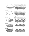
- 1 base layer
- 2 adhesive layer
- 3 solder powder
- 4 filler
- 5 solder transfer substrate
- 6 semiconductor element
- 7 low-dielectric-constant film
- 8 protruding electrode
- 9 insulating film
- 10 flux (flux material)
- 11 circuit board
- 12 electrode pad
- 13 solder resist
- 15 solder transfer substrate
- 51 support medium
- 52 adhesive
- 53 powder solder
- 54 brush
- 55 work
- 56 soldering part
- 57 spray fluxer
- 58 liquid flux
- 59 resist
- 62 adhesive
- 63 powder solder
- 65 solder transfer substrate
- 66 semiconductor element
- 67 low-dielectric-constant film
- 68 protruding electrode
Claims (2)
Applications Claiming Priority (3)
| Application Number | Priority Date | Filing Date | Title |
|---|---|---|---|
| JP2010-249576 | 2010-11-08 | ||
| JP2010249576 | 2010-11-08 | ||
| PCT/JP2011/004731 WO2012063386A1 (en) | 2010-11-08 | 2011-08-25 | Production method for solder transfer base material, solder precoating method, and solder transfer base material |
Publications (2)
| Publication Number | Publication Date |
|---|---|
| US20130181041A1 US20130181041A1 (en) | 2013-07-18 |
| US9027822B2 true US9027822B2 (en) | 2015-05-12 |
Family
ID=46050559
Family Applications (1)
| Application Number | Title | Priority Date | Filing Date |
|---|---|---|---|
| US13/822,708 Expired - Fee Related US9027822B2 (en) | 2010-11-08 | 2011-08-25 | Manufacturing method of solder transfer substrate, solder precoating method, and solder transfer substrate |
Country Status (6)
| Country | Link |
|---|---|
| US (1) | US9027822B2 (en) |
| JP (1) | JP5536899B2 (en) |
| KR (1) | KR101530528B1 (en) |
| CN (1) | CN103180079B (en) |
| TW (1) | TWI517272B (en) |
| WO (1) | WO2012063386A1 (en) |
Families Citing this family (8)
| Publication number | Priority date | Publication date | Assignee | Title |
|---|---|---|---|---|
| JP6009350B2 (en) * | 2012-12-28 | 2016-10-19 | 花王株式会社 | Circuit board manufacturing method with electronic components joined |
| JP6042214B2 (en) * | 2013-01-15 | 2016-12-14 | 倉本 武夫 | Solder bump manufacturing method and transfer sheet or release sheet used therefor |
| US10722965B2 (en) * | 2013-06-26 | 2020-07-28 | Senju Metal Industry Co., Ltd. | Solder ball supplying method, solder ball supplying device, and solder bump forming method |
| KR101930302B1 (en) * | 2013-11-05 | 2018-12-18 | 니타 가부시키가이샤 | Solder transfer sheet |
| JP5944979B1 (en) * | 2014-12-26 | 2016-07-05 | 千住金属工業株式会社 | Solder transfer sheet, solder bump, and solder pre-coating method using solder transfer sheet |
| KR102038377B1 (en) | 2015-02-11 | 2019-10-31 | 알파 어셈블리 솔루션스 인크. | Electrical connection tape |
| CN111902237B (en) * | 2018-01-19 | 2022-04-26 | Ncc纳诺责任有限公司 | Method for curing solder paste on hot brittle substrate |
| KR102422569B1 (en) * | 2019-12-27 | 2022-07-20 | 주식회사 아모그린텍 | Ribbon for brazing and manufacturing method thereof |
Citations (16)
| Publication number | Priority date | Publication date | Assignee | Title |
|---|---|---|---|---|
| JPH0574846A (en) | 1991-07-14 | 1993-03-26 | Sony Chem Corp | Electrically connecting method |
| JPH0575250A (en) | 1991-07-14 | 1993-03-26 | Sony Chem Corp | Electrical connecting method |
| JPH05198933A (en) | 1992-01-20 | 1993-08-06 | Showa Denko Kk | Solder pattern transfer film and its manufacture |
| JPH0794853A (en) | 1993-09-25 | 1995-04-07 | Tanaka Kikinzoku Kogyo Kk | Solder coating method on metal terminal of printed wiring board |
| US5591037A (en) | 1994-05-31 | 1997-01-07 | Lucent Technologies Inc. | Method for interconnecting an electronic device using a removable solder carrying medium |
| JPH0955578A (en) | 1995-08-14 | 1997-02-25 | Showa Denko Kk | Sheet applied with powder solder and formation of solder circuit |
| JPH10233463A (en) | 1997-01-27 | 1998-09-02 | Toshiba Corp | Semiconductor device and its manufacture |
| US5846366A (en) | 1994-05-31 | 1998-12-08 | Lucent Technologies Inc. | Method for interconnecting an electronic device using a transferable solder carrying medium |
| JP2000094179A (en) | 1998-09-22 | 2000-04-04 | Harima Chem Inc | Solder paste and manufacture of the same and method for solder precoating |
| JP2005011884A (en) | 2003-06-17 | 2005-01-13 | Shinko Electric Ind Co Ltd | Solder coating method in wiring board |
| WO2006067827A1 (en) | 2004-12-20 | 2006-06-29 | Senju Metal Industry Co., Ltd | Solder precoating method and work for electronic device |
| WO2007099866A1 (en) | 2006-03-03 | 2007-09-07 | Matsushita Electric Industrial Co., Ltd. | Electronic component mounted body, electronic component with solder bump, solder resin mixed material, electronic component mounting method and electronic component manufacturing method |
| CN101142665A (en) | 2005-03-29 | 2008-03-12 | 松下电器产业株式会社 | Flip chip mounting method and bump forming method |
| US20080165518A1 (en) * | 2005-03-16 | 2008-07-10 | Takashi Ichiryu | Flip Clip Mounting Process And Bump-Forming Process Using Electrically-Conductive Particles |
| JP2009010302A (en) | 2007-06-29 | 2009-01-15 | Senju Metal Ind Co Ltd | Method for forming solder paste layer |
| WO2010093031A1 (en) | 2009-02-13 | 2010-08-19 | 千住金属工業株式会社 | Solder bump formation on a circuit board using a transfer sheet |
-
2011
- 2011-08-25 US US13/822,708 patent/US9027822B2/en not_active Expired - Fee Related
- 2011-08-25 JP JP2012542788A patent/JP5536899B2/en not_active Expired - Fee Related
- 2011-08-25 CN CN201180050882.7A patent/CN103180079B/en not_active Expired - Fee Related
- 2011-08-25 WO PCT/JP2011/004731 patent/WO2012063386A1/en active Application Filing
- 2011-08-25 KR KR1020137008045A patent/KR101530528B1/en active IP Right Grant
- 2011-09-13 TW TW100132811A patent/TWI517272B/en not_active IP Right Cessation
Patent Citations (25)
| Publication number | Priority date | Publication date | Assignee | Title |
|---|---|---|---|---|
| JPH0574846A (en) | 1991-07-14 | 1993-03-26 | Sony Chem Corp | Electrically connecting method |
| JPH0575250A (en) | 1991-07-14 | 1993-03-26 | Sony Chem Corp | Electrical connecting method |
| JPH05198933A (en) | 1992-01-20 | 1993-08-06 | Showa Denko Kk | Solder pattern transfer film and its manufacture |
| JPH0794853A (en) | 1993-09-25 | 1995-04-07 | Tanaka Kikinzoku Kogyo Kk | Solder coating method on metal terminal of printed wiring board |
| US5591037A (en) | 1994-05-31 | 1997-01-07 | Lucent Technologies Inc. | Method for interconnecting an electronic device using a removable solder carrying medium |
| US5846366A (en) | 1994-05-31 | 1998-12-08 | Lucent Technologies Inc. | Method for interconnecting an electronic device using a transferable solder carrying medium |
| JPH0955578A (en) | 1995-08-14 | 1997-02-25 | Showa Denko Kk | Sheet applied with powder solder and formation of solder circuit |
| JPH10233463A (en) | 1997-01-27 | 1998-09-02 | Toshiba Corp | Semiconductor device and its manufacture |
| JP2000094179A (en) | 1998-09-22 | 2000-04-04 | Harima Chem Inc | Solder paste and manufacture of the same and method for solder precoating |
| JP2005011884A (en) | 2003-06-17 | 2005-01-13 | Shinko Electric Ind Co Ltd | Solder coating method in wiring board |
| CN101084083A (en) | 2004-12-20 | 2007-12-05 | 千住金属工业株式会社 | Solder precoating method and work for electronic device |
| WO2006067827A1 (en) | 2004-12-20 | 2006-06-29 | Senju Metal Industry Co., Ltd | Solder precoating method and work for electronic device |
| US20080213613A1 (en) | 2004-12-20 | 2008-09-04 | Takeo Kuramoto | Solder Precoating Method and Workpiece For Electronic Equipment |
| US20080165518A1 (en) * | 2005-03-16 | 2008-07-10 | Takashi Ichiryu | Flip Clip Mounting Process And Bump-Forming Process Using Electrically-Conductive Particles |
| CN100533701C (en) | 2005-03-16 | 2009-08-26 | 松下电器产业株式会社 | Method of flip chip mounting using conductive grain |
| US20090117688A1 (en) | 2005-03-29 | 2009-05-07 | Seiji Karashima | Flip chip mounting method and bump forming method |
| CN101142665A (en) | 2005-03-29 | 2008-03-12 | 松下电器产业株式会社 | Flip chip mounting method and bump forming method |
| US20080284046A1 (en) | 2005-03-29 | 2008-11-20 | Matsushita Electric Industrial Co., Ltd. | Flip chip mounting method and bump forming method |
| US20090008776A1 (en) | 2006-03-03 | 2009-01-08 | Takashi Kitae | Electronic Component Mounted Body, Electronic Component with Solder Bump, Solder Resin Mixed Material, Electronic Component Mounting Method and Electronic Component Manufacturing Method |
| CN101395976A (en) | 2006-03-03 | 2009-03-25 | 松下电器产业株式会社 | Electronic component mounted body, electronic component with solder bump, solder resin mixed material, electronic component mounting method and electronic component manufacturing method |
| KR20090004883A (en) | 2006-03-03 | 2009-01-12 | 파나소닉 주식회사 | Electronic component mounted body, electronic component with solder bump, solder resin mixed material, electronic component mounting method and electronic component manufacturing method |
| WO2007099866A1 (en) | 2006-03-03 | 2007-09-07 | Matsushita Electric Industrial Co., Ltd. | Electronic component mounted body, electronic component with solder bump, solder resin mixed material, electronic component mounting method and electronic component manufacturing method |
| JP2009010302A (en) | 2007-06-29 | 2009-01-15 | Senju Metal Ind Co Ltd | Method for forming solder paste layer |
| WO2010093031A1 (en) | 2009-02-13 | 2010-08-19 | 千住金属工業株式会社 | Solder bump formation on a circuit board using a transfer sheet |
| US20110297433A1 (en) | 2009-02-13 | 2011-12-08 | Senju Metal Industry Co., Ltd. | Solder bump formation on a circuit board using a transfer sheet |
Non-Patent Citations (4)
| Title |
|---|
| CN Office Action for 2011800508827, Nov. 26, 2014, Panasonic Corporation. |
| CN Search Report for 2011800508827, Nov. 26, 2014, Panasonic Corporation. |
| International Search Report for Application No. PCT/JP2011/004731 dated Nov. 22, 2011. |
| Korean Office Action for Application No. KR 10-2013-7008045, dated Jun. 10, 2014. |
Also Published As
| Publication number | Publication date |
|---|---|
| KR20130063017A (en) | 2013-06-13 |
| US20130181041A1 (en) | 2013-07-18 |
| CN103180079A (en) | 2013-06-26 |
| KR101530528B1 (en) | 2015-06-22 |
| WO2012063386A1 (en) | 2012-05-18 |
| TW201230217A (en) | 2012-07-16 |
| JPWO2012063386A1 (en) | 2014-05-12 |
| CN103180079B (en) | 2016-03-30 |
| JP5536899B2 (en) | 2014-07-02 |
| TWI517272B (en) | 2016-01-11 |
Similar Documents
| Publication | Publication Date | Title |
|---|---|---|
| US9027822B2 (en) | Manufacturing method of solder transfer substrate, solder precoating method, and solder transfer substrate | |
| US8324740B2 (en) | Semiconductor device, and method of manufacturing multilayer wiring board and semiconductor device | |
| CN100399558C (en) | Semiconductor device and manufacturing method of the same | |
| KR100545008B1 (en) | Semiconductor element and a producing method for the same, and a semiconductor device and a producing method for the same | |
| TWI496259B (en) | Flip chip package assembly and process for making same | |
| TWI523127B (en) | Manufacturing method for electronic device | |
| TW200525666A (en) | Bump-on-lead flip chip interconnection | |
| US20090007425A1 (en) | Method for Manufacturing Multilayer Wiring Board | |
| KR100636364B1 (en) | Bonding method for solder-pad in flip-chip package | |
| JP4337358B2 (en) | Intermediate wiring member for stacking, wiring board, and manufacturing method thereof | |
| JP6586952B2 (en) | Semiconductor device and manufacturing method thereof | |
| US20130277828A1 (en) | Methods and Apparatus for bump-on-trace Chip Packaging | |
| US9238278B2 (en) | Solder transfer substrate, manufacturing method of solder transfer substrate, and solder transfer method | |
| JP2006005322A (en) | Part mounting wiring board and method for mounting part to wiring board | |
| JP4051570B2 (en) | Manufacturing method of semiconductor device | |
| JP2581456B2 (en) | Component connection structure and method of manufacturing the same | |
| JP5541157B2 (en) | Mounting substrate, substrate, and manufacturing method thereof | |
| JP2012164934A (en) | Circuit module, electronic component mounting board and circuit module manufacturing method | |
| JP7347440B2 (en) | Manufacturing method of wiring board for semiconductor package | |
| JP7052464B2 (en) | Manufacturing method of coreless substrate with fine wiring layer and manufacturing method of semiconductor package | |
| JP2012124427A (en) | Manufacturing method of electronic component and manufacturing method of semiconductor device | |
| JP3742732B2 (en) | Mounting board and mounting structure | |
| WO2021117898A1 (en) | Method for manufacturing electronic component | |
| KR100775121B1 (en) | Bump structure and chip connecting method using the same | |
| JP2004087922A (en) | Substrate for semiconductor packages, and its manufacturing method |
Legal Events
| Date | Code | Title | Description |
|---|---|---|---|
| AS | Assignment |
Owner name: PANASONIC CORPORATION, JAPAN Free format text: ASSIGNMENT OF ASSIGNORS INTEREST;ASSIGNOR:SAKURAI, DAISUKE;REEL/FRAME:030488/0108 Effective date: 20130221 |
|
| AS | Assignment |
Owner name: PANASONIC INTELLECTUAL PROPERTY MANAGEMENT CO., LTD., JAPAN Free format text: ASSIGNMENT OF ASSIGNORS INTEREST;ASSIGNOR:PANASONIC CORPORATION;REEL/FRAME:034194/0143 Effective date: 20141110 Owner name: PANASONIC INTELLECTUAL PROPERTY MANAGEMENT CO., LT Free format text: ASSIGNMENT OF ASSIGNORS INTEREST;ASSIGNOR:PANASONIC CORPORATION;REEL/FRAME:034194/0143 Effective date: 20141110 |
|
| STCF | Information on status: patent grant |
Free format text: PATENTED CASE |
|
| MAFP | Maintenance fee payment |
Free format text: PAYMENT OF MAINTENANCE FEE, 4TH YEAR, LARGE ENTITY (ORIGINAL EVENT CODE: M1551); ENTITY STATUS OF PATENT OWNER: LARGE ENTITY Year of fee payment: 4 |
|
| AS | Assignment |
Owner name: PANASONIC INTELLECTUAL PROPERTY MANAGEMENT CO., LTD., JAPAN Free format text: CORRECTIVE ASSIGNMENT TO CORRECT THE ERRONEOUSLY FILED APPLICATION NUMBERS 13/384239, 13/498734, 14/116681 AND 14/301144 PREVIOUSLY RECORDED ON REEL 034194 FRAME 0143. ASSIGNOR(S) HEREBY CONFIRMS THE ASSIGNMENT;ASSIGNOR:PANASONIC CORPORATION;REEL/FRAME:056788/0362 Effective date: 20141110 |
|
| FEPP | Fee payment procedure |
Free format text: MAINTENANCE FEE REMINDER MAILED (ORIGINAL EVENT CODE: REM.); ENTITY STATUS OF PATENT OWNER: LARGE ENTITY |
|
| LAPS | Lapse for failure to pay maintenance fees |
Free format text: PATENT EXPIRED FOR FAILURE TO PAY MAINTENANCE FEES (ORIGINAL EVENT CODE: EXP.); ENTITY STATUS OF PATENT OWNER: LARGE ENTITY |
|
| STCH | Information on status: patent discontinuation |
Free format text: PATENT EXPIRED DUE TO NONPAYMENT OF MAINTENANCE FEES UNDER 37 CFR 1.362 |
|
| FP | Lapsed due to failure to pay maintenance fee |
Effective date: 20230512 |