US9035287B2 - Polymeric materials for use in metal-oxide-semiconductor field-effect transistors - Google Patents
Polymeric materials for use in metal-oxide-semiconductor field-effect transistors Download PDFInfo
- Publication number
- US9035287B2 US9035287B2 US13/844,129 US201313844129A US9035287B2 US 9035287 B2 US9035287 B2 US 9035287B2 US 201313844129 A US201313844129 A US 201313844129A US 9035287 B2 US9035287 B2 US 9035287B2
- Authority
- US
- United States
- Prior art keywords
- group
- moiety
- polysulfone
- polymer
- divalent
- Prior art date
- Legal status (The legal status is an assumption and is not a legal conclusion. Google has not performed a legal analysis and makes no representation as to the accuracy of the status listed.)
- Active, expires
Links
- 239000004065 semiconductor Substances 0.000 title claims abstract description 88
- 239000000463 material Substances 0.000 title claims abstract description 50
- 230000005669 field effect Effects 0.000 title abstract description 18
- 229920002492 poly(sulfone) Polymers 0.000 claims abstract description 94
- 238000002161 passivation Methods 0.000 claims abstract description 36
- 230000003287 optical effect Effects 0.000 claims abstract description 6
- 230000005693 optoelectronics Effects 0.000 claims abstract description 4
- 229920000642 polymer Polymers 0.000 claims description 134
- 125000003118 aryl group Chemical group 0.000 claims description 58
- 239000000758 substrate Substances 0.000 claims description 40
- 239000010409 thin film Substances 0.000 claims description 34
- 125000000008 (C1-C10) alkyl group Chemical group 0.000 claims description 30
- 229910044991 metal oxide Inorganic materials 0.000 claims description 30
- 150000004706 metal oxides Chemical class 0.000 claims description 30
- 125000001188 haloalkyl group Chemical group 0.000 claims description 26
- 229910052736 halogen Inorganic materials 0.000 claims description 23
- 150000002367 halogens Chemical class 0.000 claims description 22
- 229910052739 hydrogen Inorganic materials 0.000 claims description 19
- 125000001424 substituent group Chemical group 0.000 claims description 14
- 125000000041 C6-C10 aryl group Chemical group 0.000 claims description 9
- 239000004593 Epoxy Substances 0.000 claims description 7
- NIXOWILDQLNWCW-UHFFFAOYSA-M acrylate group Chemical group C(C=C)(=O)[O-] NIXOWILDQLNWCW-UHFFFAOYSA-M 0.000 claims description 7
- 229910052786 argon Inorganic materials 0.000 claims description 7
- 125000002534 ethynyl group Chemical group [H]C#C* 0.000 claims description 7
- 125000001997 phenyl group Chemical group [H]C1=C([H])C([H])=C(*)C([H])=C1[H] 0.000 claims description 7
- 125000000391 vinyl group Chemical group [H]C([*])=C([H])[H] 0.000 claims description 7
- 125000000332 coumarinyl group Chemical group O1C(=O)C(=CC2=CC=CC=C12)* 0.000 claims description 6
- 229910052731 fluorine Inorganic materials 0.000 claims description 6
- 125000000027 (C1-C10) alkoxy group Chemical group 0.000 claims description 5
- XLOMVQKBTHCTTD-UHFFFAOYSA-N zinc oxide Inorganic materials [Zn]=O XLOMVQKBTHCTTD-UHFFFAOYSA-N 0.000 claims description 5
- 125000003837 (C1-C20) alkyl group Chemical group 0.000 claims description 4
- 229910052727 yttrium Inorganic materials 0.000 claims description 4
- 239000011787 zinc oxide Substances 0.000 claims description 3
- 125000006267 biphenyl group Chemical group 0.000 claims description 2
- 125000001624 naphthyl group Chemical group 0.000 claims description 2
- -1 polymers) Chemical class 0.000 description 161
- 239000010410 layer Substances 0.000 description 153
- OKKJLVBELUTLKV-UHFFFAOYSA-N Methanol Chemical compound OC OKKJLVBELUTLKV-UHFFFAOYSA-N 0.000 description 99
- 239000000203 mixture Substances 0.000 description 80
- 238000000034 method Methods 0.000 description 72
- 239000010408 film Substances 0.000 description 69
- YMWUJEATGCHHMB-UHFFFAOYSA-N Dichloromethane Chemical compound ClCCl YMWUJEATGCHHMB-UHFFFAOYSA-N 0.000 description 55
- 239000007787 solid Substances 0.000 description 47
- 239000003989 dielectric material Substances 0.000 description 38
- VLKZOEOYAKHREP-UHFFFAOYSA-N n-Hexane Chemical class CCCCCC VLKZOEOYAKHREP-UHFFFAOYSA-N 0.000 description 38
- 238000006243 chemical reaction Methods 0.000 description 34
- 230000008569 process Effects 0.000 description 34
- HEDRZPFGACZZDS-MICDWDOJSA-N Trichloro(2H)methane Chemical compound [2H]C(Cl)(Cl)Cl HEDRZPFGACZZDS-MICDWDOJSA-N 0.000 description 30
- 238000000151 deposition Methods 0.000 description 29
- 238000007639 printing Methods 0.000 description 27
- MVPPADPHJFYWMZ-UHFFFAOYSA-N chlorobenzene Chemical compound ClC1=CC=CC=C1 MVPPADPHJFYWMZ-UHFFFAOYSA-N 0.000 description 26
- 125000000217 alkyl group Chemical group 0.000 description 25
- XLYOFNOQVPJJNP-UHFFFAOYSA-N water Substances O XLYOFNOQVPJJNP-UHFFFAOYSA-N 0.000 description 24
- 150000001875 compounds Chemical class 0.000 description 23
- 238000004132 cross linking Methods 0.000 description 22
- 230000015572 biosynthetic process Effects 0.000 description 21
- 238000005160 1H NMR spectroscopy Methods 0.000 description 20
- IJGRMHOSHXDMSA-UHFFFAOYSA-N Atomic nitrogen Chemical compound N#N IJGRMHOSHXDMSA-UHFFFAOYSA-N 0.000 description 20
- 230000005855 radiation Effects 0.000 description 20
- 238000001723 curing Methods 0.000 description 19
- 239000012071 phase Substances 0.000 description 19
- 229920001577 copolymer Polymers 0.000 description 17
- 238000004528 spin coating Methods 0.000 description 17
- 239000004971 Cross linker Substances 0.000 description 16
- 238000005227 gel permeation chromatography Methods 0.000 description 16
- 238000010438 heat treatment Methods 0.000 description 16
- 239000000126 substance Substances 0.000 description 16
- WYURNTSHIVDZCO-UHFFFAOYSA-N tetrahydrofuran Substances C1CCOC1 WYURNTSHIVDZCO-UHFFFAOYSA-N 0.000 description 16
- 125000004432 carbon atom Chemical group C* 0.000 description 14
- XLJMAIOERFSOGZ-UHFFFAOYSA-M cyanate Chemical compound [O-]C#N XLJMAIOERFSOGZ-UHFFFAOYSA-M 0.000 description 14
- 125000001072 heteroaryl group Chemical group 0.000 description 14
- 229910052757 nitrogen Inorganic materials 0.000 description 14
- 238000003786 synthesis reaction Methods 0.000 description 14
- SECXISVLQFMRJM-UHFFFAOYSA-N N-Methylpyrrolidone Chemical compound CN1CCCC1=O SECXISVLQFMRJM-UHFFFAOYSA-N 0.000 description 13
- 239000011248 coating agent Substances 0.000 description 13
- 238000000576 coating method Methods 0.000 description 13
- 230000009477 glass transition Effects 0.000 description 13
- 239000007788 liquid Substances 0.000 description 13
- 238000004519 manufacturing process Methods 0.000 description 13
- 229910052751 metal Inorganic materials 0.000 description 13
- 239000002184 metal Substances 0.000 description 13
- 150000003384 small molecules Chemical class 0.000 description 13
- 239000002904 solvent Substances 0.000 description 13
- QTBSBXVTEAMEQO-UHFFFAOYSA-N Acetic acid Chemical compound CC(O)=O QTBSBXVTEAMEQO-UHFFFAOYSA-N 0.000 description 12
- 239000004697 Polyetherimide Substances 0.000 description 12
- JUJWROOIHBZHMG-UHFFFAOYSA-N Pyridine Chemical compound C1=CC=NC=C1 JUJWROOIHBZHMG-UHFFFAOYSA-N 0.000 description 12
- BGTOWKSIORTVQH-UHFFFAOYSA-N cyclopentanone Chemical compound O=C1CCCC1 BGTOWKSIORTVQH-UHFFFAOYSA-N 0.000 description 12
- 229920001601 polyetherimide Polymers 0.000 description 12
- 238000000137 annealing Methods 0.000 description 11
- 125000000753 cycloalkyl group Chemical group 0.000 description 11
- 238000000354 decomposition reaction Methods 0.000 description 11
- 229910052760 oxygen Inorganic materials 0.000 description 11
- 229920002120 photoresistant polymer Polymers 0.000 description 11
- LAQYHRQFABOIFD-UHFFFAOYSA-N 2-methoxyhydroquinone Chemical compound COC1=CC(O)=CC=C1O LAQYHRQFABOIFD-UHFFFAOYSA-N 0.000 description 10
- VYPSYNLAJGMNEJ-UHFFFAOYSA-N Silicium dioxide Chemical class O=[Si]=O VYPSYNLAJGMNEJ-UHFFFAOYSA-N 0.000 description 10
- 125000003342 alkenyl group Chemical group 0.000 description 10
- 125000000304 alkynyl group Chemical group 0.000 description 10
- 238000000921 elemental analysis Methods 0.000 description 10
- 125000000956 methoxy group Chemical group [H]C([H])([H])O* 0.000 description 10
- 238000000059 patterning Methods 0.000 description 10
- BWHMMNNQKKPAPP-UHFFFAOYSA-L potassium carbonate Chemical compound [K+].[K+].[O-]C([O-])=O BWHMMNNQKKPAPP-UHFFFAOYSA-L 0.000 description 10
- CSCPPACGZOOCGX-UHFFFAOYSA-N Acetone Chemical compound CC(C)=O CSCPPACGZOOCGX-UHFFFAOYSA-N 0.000 description 9
- IAZDPXIOMUYVGZ-WFGJKAKNSA-N Dimethyl sulfoxide Chemical compound [2H]C([2H])([2H])S(=O)C([2H])([2H])[2H] IAZDPXIOMUYVGZ-WFGJKAKNSA-N 0.000 description 9
- MUBZPKHOEPUJKR-UHFFFAOYSA-N Oxalic acid Chemical compound OC(=O)C(O)=O MUBZPKHOEPUJKR-UHFFFAOYSA-N 0.000 description 9
- 239000003153 chemical reaction reagent Substances 0.000 description 9
- 239000008199 coating composition Substances 0.000 description 9
- 238000001914 filtration Methods 0.000 description 9
- 238000009472 formulation Methods 0.000 description 9
- 125000000623 heterocyclic group Chemical group 0.000 description 9
- 238000000206 photolithography Methods 0.000 description 9
- 229910052710 silicon Inorganic materials 0.000 description 9
- HXJUTPCZVOIRIF-UHFFFAOYSA-N sulfolane Chemical compound O=S1(=O)CCCC1 HXJUTPCZVOIRIF-UHFFFAOYSA-N 0.000 description 9
- VTYYLEPIZMXCLO-UHFFFAOYSA-L Calcium carbonate Chemical compound [Ca+2].[O-]C([O-])=O VTYYLEPIZMXCLO-UHFFFAOYSA-L 0.000 description 8
- XUIMIQQOPSSXEZ-UHFFFAOYSA-N Silicon Chemical compound [Si] XUIMIQQOPSSXEZ-UHFFFAOYSA-N 0.000 description 8
- QVGXLLKOCUKJST-UHFFFAOYSA-N atomic oxygen Chemical compound [O] QVGXLLKOCUKJST-UHFFFAOYSA-N 0.000 description 8
- 125000004122 cyclic group Chemical group 0.000 description 8
- 125000000524 functional group Chemical group 0.000 description 8
- 239000011521 glass Substances 0.000 description 8
- 239000001301 oxygen Substances 0.000 description 8
- 229920003229 poly(methyl methacrylate) Polymers 0.000 description 8
- 239000004926 polymethyl methacrylate Substances 0.000 description 8
- 239000011541 reaction mixture Substances 0.000 description 8
- 239000010703 silicon Substances 0.000 description 8
- 238000004544 sputter deposition Methods 0.000 description 8
- 238000003756 stirring Methods 0.000 description 8
- WGTYBPLFGIVFAS-UHFFFAOYSA-M tetramethylammonium hydroxide Chemical compound [OH-].C[N+](C)(C)C WGTYBPLFGIVFAS-UHFFFAOYSA-M 0.000 description 8
- 238000002411 thermogravimetry Methods 0.000 description 8
- 125000003710 aryl alkyl group Chemical group 0.000 description 7
- 239000002585 base Substances 0.000 description 7
- 230000008901 benefit Effects 0.000 description 7
- 239000012043 crude product Substances 0.000 description 7
- 230000008021 deposition Effects 0.000 description 7
- 239000000706 filtrate Substances 0.000 description 7
- 230000006870 function Effects 0.000 description 7
- 125000005842 heteroatom Chemical group 0.000 description 7
- 239000011229 interlayer Substances 0.000 description 7
- 239000003960 organic solvent Substances 0.000 description 7
- 229910052717 sulfur Inorganic materials 0.000 description 7
- 239000000725 suspension Substances 0.000 description 7
- XKRFYHLGVUSROY-UHFFFAOYSA-N Argon Chemical compound [Ar] XKRFYHLGVUSROY-UHFFFAOYSA-N 0.000 description 6
- RTZKZFJDLAIYFH-UHFFFAOYSA-N Diethyl ether Chemical compound CCOCC RTZKZFJDLAIYFH-UHFFFAOYSA-N 0.000 description 6
- CSNNHWWHGAXBCP-UHFFFAOYSA-L Magnesium sulfate Chemical compound [Mg+2].[O-][S+2]([O-])([O-])[O-] CSNNHWWHGAXBCP-UHFFFAOYSA-L 0.000 description 6
- 239000004693 Polybenzimidazole Substances 0.000 description 6
- 239000003570 air Substances 0.000 description 6
- 125000002837 carbocyclic group Chemical group 0.000 description 6
- 125000005843 halogen group Chemical group 0.000 description 6
- 239000005457 ice water Substances 0.000 description 6
- 125000002496 methyl group Chemical group [H]C([H])([H])* 0.000 description 6
- 239000011368 organic material Substances 0.000 description 6
- 239000003504 photosensitizing agent Substances 0.000 description 6
- 229920002480 polybenzimidazole Polymers 0.000 description 6
- 125000003367 polycyclic group Chemical group 0.000 description 6
- UMJSCPRVCHMLSP-UHFFFAOYSA-N pyridine Natural products COC1=CC=CN=C1 UMJSCPRVCHMLSP-UHFFFAOYSA-N 0.000 description 6
- 150000003254 radicals Chemical class 0.000 description 6
- 238000012546 transfer Methods 0.000 description 6
- 235000012431 wafers Nutrition 0.000 description 6
- QGZKDVFQNNGYKY-UHFFFAOYSA-N Ammonia Chemical compound N QGZKDVFQNNGYKY-UHFFFAOYSA-N 0.000 description 5
- XEKOWRVHYACXOJ-UHFFFAOYSA-N Ethyl acetate Chemical compound CCOC(C)=O XEKOWRVHYACXOJ-UHFFFAOYSA-N 0.000 description 5
- ZMXDDKWLCZADIW-UHFFFAOYSA-N N,N-Dimethylformamide Chemical compound CN(C)C=O ZMXDDKWLCZADIW-UHFFFAOYSA-N 0.000 description 5
- 239000012298 atmosphere Substances 0.000 description 5
- 125000004429 atom Chemical group 0.000 description 5
- 239000003990 capacitor Substances 0.000 description 5
- 230000015556 catabolic process Effects 0.000 description 5
- 239000010949 copper Substances 0.000 description 5
- 238000005538 encapsulation Methods 0.000 description 5
- 238000005530 etching Methods 0.000 description 5
- 238000007646 gravure printing Methods 0.000 description 5
- 125000004435 hydrogen atom Chemical group [H]* 0.000 description 5
- 238000007641 inkjet printing Methods 0.000 description 5
- 238000001755 magnetron sputter deposition Methods 0.000 description 5
- 239000011159 matrix material Substances 0.000 description 5
- 238000005259 measurement Methods 0.000 description 5
- 150000002739 metals Chemical class 0.000 description 5
- 125000002950 monocyclic group Chemical group 0.000 description 5
- 229920000036 polyvinylpyrrolidone Polymers 0.000 description 5
- 235000013855 polyvinylpyrrolidone Nutrition 0.000 description 5
- 229910000027 potassium carbonate Inorganic materials 0.000 description 5
- 238000012545 processing Methods 0.000 description 5
- 239000006228 supernatant Substances 0.000 description 5
- PLVUIVUKKJTSDM-UHFFFAOYSA-N 1-fluoro-4-(4-fluorophenyl)sulfonylbenzene Chemical compound C1=CC(F)=CC=C1S(=O)(=O)C1=CC=C(F)C=C1 PLVUIVUKKJTSDM-UHFFFAOYSA-N 0.000 description 4
- OZAIFHULBGXAKX-UHFFFAOYSA-N 2-(2-cyanopropan-2-yldiazenyl)-2-methylpropanenitrile Chemical compound N#CC(C)(C)N=NC(C)(C)C#N OZAIFHULBGXAKX-UHFFFAOYSA-N 0.000 description 4
- ZWEHNKRNPOVVGH-UHFFFAOYSA-N 2-Butanone Chemical compound CCC(C)=O ZWEHNKRNPOVVGH-UHFFFAOYSA-N 0.000 description 4
- YEJRWHAVMIAJKC-UHFFFAOYSA-N 4-Butyrolactone Chemical compound O=C1CCCO1 YEJRWHAVMIAJKC-UHFFFAOYSA-N 0.000 description 4
- ZOKXTWBITQBERF-UHFFFAOYSA-N Molybdenum Chemical compound [Mo] ZOKXTWBITQBERF-UHFFFAOYSA-N 0.000 description 4
- 239000004642 Polyimide Substances 0.000 description 4
- UIIMBOGNXHQVGW-UHFFFAOYSA-M Sodium bicarbonate Chemical compound [Na+].OC([O-])=O UIIMBOGNXHQVGW-UHFFFAOYSA-M 0.000 description 4
- RDOXTESZEPMUJZ-UHFFFAOYSA-N anisole Chemical compound COC1=CC=CC=C1 RDOXTESZEPMUJZ-UHFFFAOYSA-N 0.000 description 4
- ILAHWRKJUDSMFH-UHFFFAOYSA-N boron tribromide Chemical compound BrB(Br)Br ILAHWRKJUDSMFH-UHFFFAOYSA-N 0.000 description 4
- 229910000019 calcium carbonate Inorganic materials 0.000 description 4
- 239000011203 carbon fibre reinforced carbon Substances 0.000 description 4
- 238000005266 casting Methods 0.000 description 4
- 150000004770 chalcogenides Chemical class 0.000 description 4
- 239000002131 composite material Substances 0.000 description 4
- JHIVVAPYMSGYDF-UHFFFAOYSA-N cyclohexanone Chemical compound O=C1CCCCC1 JHIVVAPYMSGYDF-UHFFFAOYSA-N 0.000 description 4
- 238000003618 dip coating Methods 0.000 description 4
- KZTYYGOKRVBIMI-UHFFFAOYSA-N diphenyl sulfone Chemical group C=1C=CC=CC=1S(=O)(=O)C1=CC=CC=C1 KZTYYGOKRVBIMI-UHFFFAOYSA-N 0.000 description 4
- 229910003437 indium oxide Inorganic materials 0.000 description 4
- PJXISJQVUVHSOJ-UHFFFAOYSA-N indium(iii) oxide Chemical compound [O-2].[O-2].[O-2].[In+3].[In+3] PJXISJQVUVHSOJ-UHFFFAOYSA-N 0.000 description 4
- 239000003999 initiator Substances 0.000 description 4
- 238000000869 ion-assisted deposition Methods 0.000 description 4
- 150000002500 ions Chemical class 0.000 description 4
- 229910052750 molybdenum Inorganic materials 0.000 description 4
- 239000011733 molybdenum Substances 0.000 description 4
- 239000012044 organic layer Substances 0.000 description 4
- 238000007649 pad printing Methods 0.000 description 4
- 229920001721 polyimide Polymers 0.000 description 4
- 238000006116 polymerization reaction Methods 0.000 description 4
- 125000006413 ring segment Chemical group 0.000 description 4
- 238000007650 screen-printing Methods 0.000 description 4
- 239000011669 selenium Substances 0.000 description 4
- WOGITNXCNOTRLK-VOTSOKGWSA-N (e)-3-phenylprop-2-enoyl chloride Chemical compound ClC(=O)\C=C\C1=CC=CC=C1 WOGITNXCNOTRLK-VOTSOKGWSA-N 0.000 description 3
- OXBLVCZKDOZZOJ-UHFFFAOYSA-N 2,3-Dihydrothiophene Chemical compound C1CC=CS1 OXBLVCZKDOZZOJ-UHFFFAOYSA-N 0.000 description 3
- UHOVQNZJYSORNB-UHFFFAOYSA-N Benzene Chemical compound C1=CC=CC=C1 UHOVQNZJYSORNB-UHFFFAOYSA-N 0.000 description 3
- RYGMFSIKBFXOCR-UHFFFAOYSA-N Copper Chemical compound [Cu] RYGMFSIKBFXOCR-UHFFFAOYSA-N 0.000 description 3
- VGGSQFUCUMXWEO-UHFFFAOYSA-N Ethene Chemical compound C=C VGGSQFUCUMXWEO-UHFFFAOYSA-N 0.000 description 3
- 239000005977 Ethylene Substances 0.000 description 3
- LRHPLDYGYMQRHN-UHFFFAOYSA-N N-Butanol Chemical compound CCCCO LRHPLDYGYMQRHN-UHFFFAOYSA-N 0.000 description 3
- YXFVVABEGXRONW-UHFFFAOYSA-N Toluene Chemical compound CC1=CC=CC=C1 YXFVVABEGXRONW-UHFFFAOYSA-N 0.000 description 3
- 125000003545 alkoxy group Chemical group 0.000 description 3
- 229910052782 aluminium Inorganic materials 0.000 description 3
- XAGFODPZIPBFFR-UHFFFAOYSA-N aluminium Chemical compound [Al] XAGFODPZIPBFFR-UHFFFAOYSA-N 0.000 description 3
- 230000004888 barrier function Effects 0.000 description 3
- 229910052794 bromium Inorganic materials 0.000 description 3
- 239000012159 carrier gas Substances 0.000 description 3
- 125000003636 chemical group Chemical group 0.000 description 3
- 239000003795 chemical substances by application Substances 0.000 description 3
- 229910052801 chlorine Inorganic materials 0.000 description 3
- 230000000052 comparative effect Effects 0.000 description 3
- 239000004020 conductor Substances 0.000 description 3
- 229910052802 copper Inorganic materials 0.000 description 3
- 150000004292 cyclic ethers Chemical group 0.000 description 3
- XNMQEEKYCVKGBD-UHFFFAOYSA-N dimethylacetylene Natural products CC#CC XNMQEEKYCVKGBD-UHFFFAOYSA-N 0.000 description 3
- 239000006185 dispersion Substances 0.000 description 3
- 238000001035 drying Methods 0.000 description 3
- 230000005684 electric field Effects 0.000 description 3
- 150000002118 epoxides Chemical class 0.000 description 3
- 239000010931 gold Substances 0.000 description 3
- 230000005484 gravity Effects 0.000 description 3
- 238000010952 in-situ formation Methods 0.000 description 3
- 229910052738 indium Inorganic materials 0.000 description 3
- APFVFJFRJDLVQX-UHFFFAOYSA-N indium atom Chemical compound [In] APFVFJFRJDLVQX-UHFFFAOYSA-N 0.000 description 3
- 229910052740 iodine Inorganic materials 0.000 description 3
- 230000000670 limiting effect Effects 0.000 description 3
- 229910052943 magnesium sulfate Inorganic materials 0.000 description 3
- 239000003607 modifier Substances 0.000 description 3
- PXHVJJICTQNCMI-UHFFFAOYSA-N nickel Substances [Ni] PXHVJJICTQNCMI-UHFFFAOYSA-N 0.000 description 3
- 238000007645 offset printing Methods 0.000 description 3
- 235000006408 oxalic acid Nutrition 0.000 description 3
- AHHWIHXENZJRFG-UHFFFAOYSA-N oxetane Chemical compound C1COC1 AHHWIHXENZJRFG-UHFFFAOYSA-N 0.000 description 3
- KDLHZDBZIXYQEI-UHFFFAOYSA-N palladium Substances [Pd] KDLHZDBZIXYQEI-UHFFFAOYSA-N 0.000 description 3
- RGSFGYAAUTVSQA-UHFFFAOYSA-N pentamethylene Natural products C1CCCC1 RGSFGYAAUTVSQA-UHFFFAOYSA-N 0.000 description 3
- 229910052698 phosphorus Inorganic materials 0.000 description 3
- 238000000623 plasma-assisted chemical vapour deposition Methods 0.000 description 3
- 229920003023 plastic Polymers 0.000 description 3
- 239000004033 plastic Substances 0.000 description 3
- 239000004848 polyfunctional curative Substances 0.000 description 3
- 239000002243 precursor Substances 0.000 description 3
- 239000000047 product Substances 0.000 description 3
- 125000006239 protecting group Chemical group 0.000 description 3
- BBFCIBZLAVOLCF-UHFFFAOYSA-N pyridin-1-ium;bromide Chemical compound Br.C1=CC=NC=C1 BBFCIBZLAVOLCF-UHFFFAOYSA-N 0.000 description 3
- 230000002829 reductive effect Effects 0.000 description 3
- 239000000523 sample Substances 0.000 description 3
- 229910052814 silicon oxide Inorganic materials 0.000 description 3
- XOLBLPGZBRYERU-UHFFFAOYSA-N tin dioxide Chemical compound O=[Sn]=O XOLBLPGZBRYERU-UHFFFAOYSA-N 0.000 description 3
- 125000002023 trifluoromethyl group Chemical group FC(F)(F)* 0.000 description 3
- 125000006649 (C2-C20) alkynyl group Chemical group 0.000 description 2
- SILNNFMWIMZVEQ-UHFFFAOYSA-N 1,3-dihydrobenzimidazol-2-one Chemical compound C1=CC=C2NC(O)=NC2=C1 SILNNFMWIMZVEQ-UHFFFAOYSA-N 0.000 description 2
- VXNZUUAINFGPBY-UHFFFAOYSA-N 1-Butene Chemical compound CCC=C VXNZUUAINFGPBY-UHFFFAOYSA-N 0.000 description 2
- BBMCTIGTTCKYKF-UHFFFAOYSA-N 1-heptanol Chemical compound CCCCCCCO BBMCTIGTTCKYKF-UHFFFAOYSA-N 0.000 description 2
- FZXRXKLUIMKDEL-UHFFFAOYSA-N 2-Methylpropyl propanoate Chemical compound CCC(=O)OCC(C)C FZXRXKLUIMKDEL-UHFFFAOYSA-N 0.000 description 2
- JESXATFQYMPTNL-UHFFFAOYSA-N 2-ethenylphenol Chemical compound OC1=CC=CC=C1C=C JESXATFQYMPTNL-UHFFFAOYSA-N 0.000 description 2
- WUPHOULIZUERAE-UHFFFAOYSA-N 3-(oxolan-2-yl)propanoic acid Chemical compound OC(=O)CCC1CCCO1 WUPHOULIZUERAE-UHFFFAOYSA-N 0.000 description 2
- NHQDETIJWKXCTC-UHFFFAOYSA-N 3-chloroperbenzoic acid Chemical compound OOC(=O)C1=CC=CC(Cl)=C1 NHQDETIJWKXCTC-UHFFFAOYSA-N 0.000 description 2
- 229920001621 AMOLED Polymers 0.000 description 2
- JBRZTFJDHDCESZ-UHFFFAOYSA-N AsGa Chemical compound [As]#[Ga] JBRZTFJDHDCESZ-UHFFFAOYSA-N 0.000 description 2
- 229910015845 BBr3 Inorganic materials 0.000 description 2
- 125000003358 C2-C20 alkenyl group Chemical group 0.000 description 2
- 125000005915 C6-C14 aryl group Chemical group 0.000 description 2
- XDTMQSROBMDMFD-UHFFFAOYSA-N Cyclohexane Chemical compound C1CCCCC1 XDTMQSROBMDMFD-UHFFFAOYSA-N 0.000 description 2
- LFQSCWFLJHTTHZ-UHFFFAOYSA-N Ethanol Chemical compound CCO LFQSCWFLJHTTHZ-UHFFFAOYSA-N 0.000 description 2
- GYHNNYVSQQEPJS-UHFFFAOYSA-N Gallium Chemical compound [Ga] GYHNNYVSQQEPJS-UHFFFAOYSA-N 0.000 description 2
- 229910001218 Gallium arsenide Inorganic materials 0.000 description 2
- UFHFLCQGNIYNRP-UHFFFAOYSA-N Hydrogen Chemical compound [H][H] UFHFLCQGNIYNRP-UHFFFAOYSA-N 0.000 description 2
- KFZMGEQAYNKOFK-UHFFFAOYSA-N Isopropanol Chemical compound CC(C)O KFZMGEQAYNKOFK-UHFFFAOYSA-N 0.000 description 2
- AFVFQIVMOAPDHO-UHFFFAOYSA-N Methanesulfonic acid Chemical compound CS(O)(=O)=O AFVFQIVMOAPDHO-UHFFFAOYSA-N 0.000 description 2
- VVQNEPGJFQJSBK-UHFFFAOYSA-N Methyl methacrylate Chemical compound COC(=O)C(C)=C VVQNEPGJFQJSBK-UHFFFAOYSA-N 0.000 description 2
- FXHOOIRPVKKKFG-UHFFFAOYSA-N N,N-Dimethylacetamide Chemical compound CN(C)C(C)=O FXHOOIRPVKKKFG-UHFFFAOYSA-N 0.000 description 2
- 238000005481 NMR spectroscopy Methods 0.000 description 2
- JCXJVPUVTGWSNB-UHFFFAOYSA-N Nitrogen dioxide Chemical compound O=[N]=O JCXJVPUVTGWSNB-UHFFFAOYSA-N 0.000 description 2
- 229920002367 Polyisobutene Polymers 0.000 description 2
- 239000004734 Polyphenylene sulfide Substances 0.000 description 2
- 239000004743 Polypropylene Substances 0.000 description 2
- 239000004793 Polystyrene Substances 0.000 description 2
- BUGBHKTXTAQXES-UHFFFAOYSA-N Selenium Chemical compound [Se] BUGBHKTXTAQXES-UHFFFAOYSA-N 0.000 description 2
- 229910052581 Si3N4 Inorganic materials 0.000 description 2
- 229910004205 SiNX Inorganic materials 0.000 description 2
- CDBYLPFSWZWCQE-UHFFFAOYSA-L Sodium Carbonate Chemical compound [Na+].[Na+].[O-]C([O-])=O CDBYLPFSWZWCQE-UHFFFAOYSA-L 0.000 description 2
- FAPWRFPIFSIZLT-UHFFFAOYSA-M Sodium chloride Chemical compound [Na+].[Cl-] FAPWRFPIFSIZLT-UHFFFAOYSA-M 0.000 description 2
- PPBRXRYQALVLMV-UHFFFAOYSA-N Styrene Chemical compound C=CC1=CC=CC=C1 PPBRXRYQALVLMV-UHFFFAOYSA-N 0.000 description 2
- NINIDFKCEFEMDL-UHFFFAOYSA-N Sulfur Chemical compound [S] NINIDFKCEFEMDL-UHFFFAOYSA-N 0.000 description 2
- YRKCREAYFQTBPV-UHFFFAOYSA-N acetylacetone Chemical compound CC(=O)CC(C)=O YRKCREAYFQTBPV-UHFFFAOYSA-N 0.000 description 2
- 238000005903 acid hydrolysis reaction Methods 0.000 description 2
- 230000002378 acidificating effect Effects 0.000 description 2
- 230000009471 action Effects 0.000 description 2
- 125000004414 alkyl thio group Chemical group 0.000 description 2
- VSCWAEJMTAWNJL-UHFFFAOYSA-K aluminium trichloride Chemical compound Cl[Al](Cl)Cl VSCWAEJMTAWNJL-UHFFFAOYSA-K 0.000 description 2
- 150000001408 amides Chemical class 0.000 description 2
- 229910021529 ammonia Inorganic materials 0.000 description 2
- 150000004945 aromatic hydrocarbons Chemical group 0.000 description 2
- 238000000231 atomic layer deposition Methods 0.000 description 2
- UMIVXZPTRXBADB-UHFFFAOYSA-N benzocyclobutene Chemical compound C1=CC=C2CCC2=C1 UMIVXZPTRXBADB-UHFFFAOYSA-N 0.000 description 2
- 125000005841 biaryl group Chemical group 0.000 description 2
- 125000002619 bicyclic group Chemical group 0.000 description 2
- 230000000903 blocking effect Effects 0.000 description 2
- 238000006664 bond formation reaction Methods 0.000 description 2
- KDKYADYSIPSCCQ-UHFFFAOYSA-N but-1-yne Chemical compound CCC#C KDKYADYSIPSCCQ-UHFFFAOYSA-N 0.000 description 2
- IAQRGUVFOMOMEM-UHFFFAOYSA-N but-2-ene Chemical compound CC=CC IAQRGUVFOMOMEM-UHFFFAOYSA-N 0.000 description 2
- 125000000484 butyl group Chemical group [H]C([*])([H])C([H])([H])C([H])([H])C([H])([H])[H] 0.000 description 2
- 229910052980 cadmium sulfide Inorganic materials 0.000 description 2
- 229910052799 carbon Inorganic materials 0.000 description 2
- ZYGHJZDHTFUPRJ-UHFFFAOYSA-N coumarin Chemical compound C1=CC=C2OC(=O)C=CC2=C1 ZYGHJZDHTFUPRJ-UHFFFAOYSA-N 0.000 description 2
- 125000001995 cyclobutyl group Chemical group [H]C1([H])C([H])([H])C([H])(*)C1([H])[H] 0.000 description 2
- 125000000113 cyclohexyl group Chemical group [H]C1([H])C([H])([H])C([H])([H])C([H])(*)C([H])([H])C1([H])[H] 0.000 description 2
- DIOQZVSQGTUSAI-UHFFFAOYSA-N decane Chemical compound CCCCCCCCCC DIOQZVSQGTUSAI-UHFFFAOYSA-N 0.000 description 2
- 230000001419 dependent effect Effects 0.000 description 2
- 238000005137 deposition process Methods 0.000 description 2
- SWXVUIWOUIDPGS-UHFFFAOYSA-N diacetone alcohol Chemical compound CC(=O)CC(C)(C)O SWXVUIWOUIDPGS-UHFFFAOYSA-N 0.000 description 2
- VFHVQBAGLAREND-UHFFFAOYSA-N diphenylphosphoryl-(2,4,6-trimethylphenyl)methanone Chemical compound CC1=CC(C)=CC(C)=C1C(=O)P(=O)(C=1C=CC=CC=1)C1=CC=CC=C1 VFHVQBAGLAREND-UHFFFAOYSA-N 0.000 description 2
- 230000000694 effects Effects 0.000 description 2
- 239000000839 emulsion Substances 0.000 description 2
- LZCLXQDLBQLTDK-UHFFFAOYSA-N ethyl 2-hydroxypropanoate Chemical compound CCOC(=O)C(C)O LZCLXQDLBQLTDK-UHFFFAOYSA-N 0.000 description 2
- MTZQAGJQAFMTAQ-UHFFFAOYSA-N ethyl benzoate Chemical compound CCOC(=O)C1=CC=CC=C1 MTZQAGJQAFMTAQ-UHFFFAOYSA-N 0.000 description 2
- 125000001495 ethyl group Chemical group [H]C([H])([H])C([H])([H])* 0.000 description 2
- FKRCODPIKNYEAC-UHFFFAOYSA-N ethyl propionate Chemical compound CCOC(=O)CC FKRCODPIKNYEAC-UHFFFAOYSA-N 0.000 description 2
- 229910052733 gallium Inorganic materials 0.000 description 2
- 229910001195 gallium oxide Inorganic materials 0.000 description 2
- 229910052732 germanium Inorganic materials 0.000 description 2
- GNPVGFCGXDBREM-UHFFFAOYSA-N germanium atom Chemical compound [Ge] GNPVGFCGXDBREM-UHFFFAOYSA-N 0.000 description 2
- 150000004676 glycans Chemical class 0.000 description 2
- 125000003106 haloaryl group Chemical group 0.000 description 2
- DMEGYFMYUHOHGS-UHFFFAOYSA-N heptamethylene Natural products C1CCCCCC1 DMEGYFMYUHOHGS-UHFFFAOYSA-N 0.000 description 2
- CATSNJVOTSVZJV-UHFFFAOYSA-N heptan-2-one Chemical compound CCCCCC(C)=O CATSNJVOTSVZJV-UHFFFAOYSA-N 0.000 description 2
- NGAZZOYFWWSOGK-UHFFFAOYSA-N heptan-3-one Chemical compound CCCCC(=O)CC NGAZZOYFWWSOGK-UHFFFAOYSA-N 0.000 description 2
- 239000001257 hydrogen Substances 0.000 description 2
- ZMZDMBWJUHKJPS-UHFFFAOYSA-N hydrogen thiocyanate Natural products SC#N ZMZDMBWJUHKJPS-UHFFFAOYSA-N 0.000 description 2
- 239000012212 insulator Substances 0.000 description 2
- 125000000959 isobutyl group Chemical group [H]C([H])([H])C([H])(C([H])([H])[H])C([H])([H])* 0.000 description 2
- 125000001449 isopropyl group Chemical group [H]C([H])([H])C([H])(*)C([H])([H])[H] 0.000 description 2
- 239000005300 metallic glass Substances 0.000 description 2
- UZKWTJUDCOPSNM-UHFFFAOYSA-N methoxybenzene Substances CCCCOC=C UZKWTJUDCOPSNM-UHFFFAOYSA-N 0.000 description 2
- QPJVMBTYPHYUOC-UHFFFAOYSA-N methyl benzoate Chemical compound COC(=O)C1=CC=CC=C1 QPJVMBTYPHYUOC-UHFFFAOYSA-N 0.000 description 2
- 238000004377 microelectronic Methods 0.000 description 2
- 125000004108 n-butyl group Chemical group [H]C([H])([H])C([H])([H])C([H])([H])C([H])([H])* 0.000 description 2
- 125000004123 n-propyl group Chemical group [H]C([H])([H])C([H])([H])C([H])([H])* 0.000 description 2
- 229910052759 nickel Inorganic materials 0.000 description 2
- 239000012299 nitrogen atmosphere Substances 0.000 description 2
- BKIMMITUMNQMOS-UHFFFAOYSA-N nonane Chemical compound CCCCCCCCC BKIMMITUMNQMOS-UHFFFAOYSA-N 0.000 description 2
- 239000012038 nucleophile Substances 0.000 description 2
- 238000000879 optical micrograph Methods 0.000 description 2
- 125000004043 oxo group Chemical group O=* 0.000 description 2
- 229910052763 palladium Inorganic materials 0.000 description 2
- XNLICIUVMPYHGG-UHFFFAOYSA-N pentan-2-one Chemical compound CCCC(C)=O XNLICIUVMPYHGG-UHFFFAOYSA-N 0.000 description 2
- FDPIMTJIUBPUKL-UHFFFAOYSA-N pentan-3-one Chemical compound CCC(=O)CC FDPIMTJIUBPUKL-UHFFFAOYSA-N 0.000 description 2
- PGMYKACGEOXYJE-UHFFFAOYSA-N pentyl acetate Chemical compound CCCCCOC(C)=O PGMYKACGEOXYJE-UHFFFAOYSA-N 0.000 description 2
- 125000005004 perfluoroethyl group Chemical group FC(F)(F)C(F)(F)* 0.000 description 2
- 238000005240 physical vapour deposition Methods 0.000 description 2
- BASFCYQUMIYNBI-UHFFFAOYSA-N platinum Chemical compound [Pt] BASFCYQUMIYNBI-UHFFFAOYSA-N 0.000 description 2
- 229920000139 polyethylene terephthalate Polymers 0.000 description 2
- 239000005020 polyethylene terephthalate Substances 0.000 description 2
- 229920000069 polyphenylene sulfide Polymers 0.000 description 2
- 229920001155 polypropylene Polymers 0.000 description 2
- 229920000379 polypropylene carbonate Polymers 0.000 description 2
- 229920001282 polysaccharide Polymers 0.000 description 2
- 239000005017 polysaccharide Substances 0.000 description 2
- 229920002223 polystyrene Polymers 0.000 description 2
- 229920000123 polythiophene Polymers 0.000 description 2
- 229920002451 polyvinyl alcohol Polymers 0.000 description 2
- 239000004800 polyvinyl chloride Substances 0.000 description 2
- 229920000915 polyvinyl chloride Polymers 0.000 description 2
- 239000002244 precipitate Substances 0.000 description 2
- 125000001436 propyl group Chemical group [H]C([*])([H])C([H])([H])C([H])([H])[H] 0.000 description 2
- LLHKCFNBLRBOGN-UHFFFAOYSA-N propylene glycol methyl ether acetate Chemical compound COCC(C)OC(C)=O LLHKCFNBLRBOGN-UHFFFAOYSA-N 0.000 description 2
- 238000004549 pulsed laser deposition Methods 0.000 description 2
- 238000010791 quenching Methods 0.000 description 2
- 230000009257 reactivity Effects 0.000 description 2
- 230000000717 retained effect Effects 0.000 description 2
- 238000012552 review Methods 0.000 description 2
- 238000001878 scanning electron micrograph Methods 0.000 description 2
- 125000002914 sec-butyl group Chemical group [H]C([H])([H])C([H])([H])C([H])(*)C([H])([H])[H] 0.000 description 2
- 229910052711 selenium Inorganic materials 0.000 description 2
- 230000035945 sensitivity Effects 0.000 description 2
- HQVNEWCFYHHQES-UHFFFAOYSA-N silicon nitride Chemical compound N12[Si]34N5[Si]62N3[Si]51N64 HQVNEWCFYHHQES-UHFFFAOYSA-N 0.000 description 2
- 238000007764 slot die coating Methods 0.000 description 2
- 229910000030 sodium bicarbonate Inorganic materials 0.000 description 2
- 238000009987 spinning Methods 0.000 description 2
- 238000005507 spraying Methods 0.000 description 2
- 238000006467 substitution reaction Methods 0.000 description 2
- 239000011593 sulfur Substances 0.000 description 2
- 238000010345 tape casting Methods 0.000 description 2
- 125000000999 tert-butyl group Chemical group [H]C([H])([H])C(*)(C([H])([H])[H])C([H])([H])[H] 0.000 description 2
- 238000002207 thermal evaporation Methods 0.000 description 2
- 238000007669 thermal treatment Methods 0.000 description 2
- 150000003573 thiols Chemical class 0.000 description 2
- ITMCEJHCFYSIIV-UHFFFAOYSA-M triflate Chemical compound [O-]S(=O)(=O)C(F)(F)F ITMCEJHCFYSIIV-UHFFFAOYSA-M 0.000 description 2
- 238000007740 vapor deposition Methods 0.000 description 2
- 239000012808 vapor phase Substances 0.000 description 2
- 238000001947 vapour-phase growth Methods 0.000 description 2
- ABDKAPXRBAPSQN-UHFFFAOYSA-N veratrole Chemical compound COC1=CC=CC=C1OC ABDKAPXRBAPSQN-UHFFFAOYSA-N 0.000 description 2
- 125000004169 (C1-C6) alkyl group Chemical group 0.000 description 1
- 125000006708 (C5-C14) heteroaryl group Chemical group 0.000 description 1
- 125000006570 (C5-C6) heteroaryl group Chemical group 0.000 description 1
- AVQQQNCBBIEMEU-UHFFFAOYSA-N 1,1,3,3-tetramethylurea Chemical compound CN(C)C(=O)N(C)C AVQQQNCBBIEMEU-UHFFFAOYSA-N 0.000 description 1
- RYHBNJHYFVUHQT-UHFFFAOYSA-N 1,4-Dioxane Chemical compound C1COCCO1 RYHBNJHYFVUHQT-UHFFFAOYSA-N 0.000 description 1
- NDOVLWQBFFJETK-UHFFFAOYSA-N 1,4-thiazinane 1,1-dioxide Chemical compound O=S1(=O)CCNCC1 NDOVLWQBFFJETK-UHFFFAOYSA-N 0.000 description 1
- YHIIJNLSGULWAA-UHFFFAOYSA-N 1,4-thiazinane 1-oxide Chemical compound O=S1CCNCC1 YHIIJNLSGULWAA-UHFFFAOYSA-N 0.000 description 1
- DURPTKYDGMDSBL-UHFFFAOYSA-N 1-butoxybutane Chemical compound CCCCOCCCC DURPTKYDGMDSBL-UHFFFAOYSA-N 0.000 description 1
- VKQJCUYEEABXNK-UHFFFAOYSA-N 1-chloro-4-propoxythioxanthen-9-one Chemical compound S1C2=CC=CC=C2C(=O)C2=C1C(OCCC)=CC=C2Cl VKQJCUYEEABXNK-UHFFFAOYSA-N 0.000 description 1
- STYHKGTUMYFCLA-UHFFFAOYSA-N 1-ethenoxybut-1-ene Chemical compound CCC=COC=C STYHKGTUMYFCLA-UHFFFAOYSA-N 0.000 description 1
- OEVVKKAVYQFQNV-UHFFFAOYSA-N 1-ethenyl-2,4-dimethylbenzene Chemical compound CC1=CC=C(C=C)C(C)=C1 OEVVKKAVYQFQNV-UHFFFAOYSA-N 0.000 description 1
- NVJUHMXYKCUMQA-UHFFFAOYSA-N 1-ethoxypropane Chemical compound CCCOCC NVJUHMXYKCUMQA-UHFFFAOYSA-N 0.000 description 1
- 125000001637 1-naphthyl group Chemical group [H]C1=C([H])C([H])=C2C(*)=C([H])C([H])=C([H])C2=C1[H] 0.000 description 1
- HFZLSTDPRQSZCQ-UHFFFAOYSA-N 1-pyrrolidin-3-ylpyrrolidine Chemical compound C1CCCN1C1CNCC1 HFZLSTDPRQSZCQ-UHFFFAOYSA-N 0.000 description 1
- SPXOTSHWBDUUMT-UHFFFAOYSA-N 138-42-1 Chemical compound OS(=O)(=O)C1=CC=C([N+]([O-])=O)C=C1 SPXOTSHWBDUUMT-UHFFFAOYSA-N 0.000 description 1
- 125000005955 1H-indazolyl group Chemical group 0.000 description 1
- UHOPWFKONJYLCF-UHFFFAOYSA-N 2-(2-sulfanylethyl)isoindole-1,3-dione Chemical compound C1=CC=C2C(=O)N(CCS)C(=O)C2=C1 UHOPWFKONJYLCF-UHFFFAOYSA-N 0.000 description 1
- LBLYYCQCTBFVLH-UHFFFAOYSA-M 2-methylbenzenesulfonate Chemical compound CC1=CC=CC=C1S([O-])(=O)=O LBLYYCQCTBFVLH-UHFFFAOYSA-M 0.000 description 1
- 125000001622 2-naphthyl group Chemical group [H]C1=C([H])C([H])=C2C([H])=C(*)C([H])=C([H])C2=C1[H] 0.000 description 1
- MGADZUXDNSDTHW-UHFFFAOYSA-N 2H-pyran Chemical compound C1OC=CC=C1 MGADZUXDNSDTHW-UHFFFAOYSA-N 0.000 description 1
- JDFDHBSESGTDAL-UHFFFAOYSA-N 3-methoxypropan-1-ol Chemical compound COCCCO JDFDHBSESGTDAL-UHFFFAOYSA-N 0.000 description 1
- GPAPPPVRLPGFEQ-UHFFFAOYSA-N 4,4'-dichlorodiphenyl sulfone Chemical compound C1=CC(Cl)=CC=C1S(=O)(=O)C1=CC=C(Cl)C=C1 GPAPPPVRLPGFEQ-UHFFFAOYSA-N 0.000 description 1
- VHYFNPMBLIVWCW-UHFFFAOYSA-N 4-Dimethylaminopyridine Chemical compound CN(C)C1=CC=NC=C1 VHYFNPMBLIVWCW-UHFFFAOYSA-N 0.000 description 1
- PXACTUVBBMDKRW-UHFFFAOYSA-M 4-bromobenzenesulfonate Chemical compound [O-]S(=O)(=O)C1=CC=C(Br)C=C1 PXACTUVBBMDKRW-UHFFFAOYSA-M 0.000 description 1
- PXACTUVBBMDKRW-UHFFFAOYSA-N 4-bromobenzenesulfonic acid Chemical compound OS(=O)(=O)C1=CC=C(Br)C=C1 PXACTUVBBMDKRW-UHFFFAOYSA-N 0.000 description 1
- OURXRFYZEOUCRM-UHFFFAOYSA-N 4-hydroxymorpholine Chemical compound ON1CCOCC1 OURXRFYZEOUCRM-UHFFFAOYSA-N 0.000 description 1
- SPXOTSHWBDUUMT-UHFFFAOYSA-M 4-nitrobenzenesulfonate Chemical compound [O-][N+](=O)C1=CC=C(S([O-])(=O)=O)C=C1 SPXOTSHWBDUUMT-UHFFFAOYSA-M 0.000 description 1
- OCKGFTQIICXDQW-ZEQRLZLVSA-N 5-[(1r)-1-hydroxy-2-[4-[(2r)-2-hydroxy-2-(4-methyl-1-oxo-3h-2-benzofuran-5-yl)ethyl]piperazin-1-yl]ethyl]-4-methyl-3h-2-benzofuran-1-one Chemical compound C1=C2C(=O)OCC2=C(C)C([C@@H](O)CN2CCN(CC2)C[C@H](O)C2=CC=C3C(=O)OCC3=C2C)=C1 OCKGFTQIICXDQW-ZEQRLZLVSA-N 0.000 description 1
- CWSZBVAUYPTXTG-UHFFFAOYSA-N 5-[6-[[3,4-dihydroxy-6-(hydroxymethyl)-5-methoxyoxan-2-yl]oxymethyl]-3,4-dihydroxy-5-[4-hydroxy-3-(2-hydroxyethoxy)-6-(hydroxymethyl)-5-methoxyoxan-2-yl]oxyoxan-2-yl]oxy-6-(hydroxymethyl)-2-methyloxane-3,4-diol Chemical compound O1C(CO)C(OC)C(O)C(O)C1OCC1C(OC2C(C(O)C(OC)C(CO)O2)OCCO)C(O)C(O)C(OC2C(OC(C)C(O)C2O)CO)O1 CWSZBVAUYPTXTG-UHFFFAOYSA-N 0.000 description 1
- VBSYMODXUFYOLA-UHFFFAOYSA-N 5-phenylpenta-2,4-dienoyl chloride Chemical compound ClC(=O)C=CC=CC1=CC=CC=C1 VBSYMODXUFYOLA-UHFFFAOYSA-N 0.000 description 1
- LPEKGGXMPWTOCB-UHFFFAOYSA-N 8beta-(2,3-epoxy-2-methylbutyryloxy)-14-acetoxytithifolin Natural products COC(=O)C(C)O LPEKGGXMPWTOCB-UHFFFAOYSA-N 0.000 description 1
- 239000004925 Acrylic resin Substances 0.000 description 1
- 229920000178 Acrylic resin Polymers 0.000 description 1
- NOWKCMXCCJGMRR-UHFFFAOYSA-N Aziridine Chemical compound C1CN1 NOWKCMXCCJGMRR-UHFFFAOYSA-N 0.000 description 1
- 229920002799 BoPET Polymers 0.000 description 1
- DKPFZGUDAPQIHT-UHFFFAOYSA-N Butyl acetate Natural products CCCCOC(C)=O DKPFZGUDAPQIHT-UHFFFAOYSA-N 0.000 description 1
- OKTJSMMVPCPJKN-UHFFFAOYSA-N Carbon Chemical compound [C] OKTJSMMVPCPJKN-UHFFFAOYSA-N 0.000 description 1
- BVKZGUZCCUSVTD-UHFFFAOYSA-L Carbonate Chemical compound [O-]C([O-])=O BVKZGUZCCUSVTD-UHFFFAOYSA-L 0.000 description 1
- VYZAMTAEIAYCRO-UHFFFAOYSA-N Chromium Chemical compound [Cr] VYZAMTAEIAYCRO-UHFFFAOYSA-N 0.000 description 1
- YYLLIJHXUHJATK-UHFFFAOYSA-N Cyclohexyl acetate Chemical compound CC(=O)OC1CCCCC1 YYLLIJHXUHJATK-UHFFFAOYSA-N 0.000 description 1
- 208000032750 Device leakage Diseases 0.000 description 1
- OIFBSDVPJOWBCH-UHFFFAOYSA-N Diethyl carbonate Chemical compound CCOC(=O)OCC OIFBSDVPJOWBCH-UHFFFAOYSA-N 0.000 description 1
- ZAFNJMIOTHYJRJ-UHFFFAOYSA-N Diisopropyl ether Chemical compound CC(C)OC(C)C ZAFNJMIOTHYJRJ-UHFFFAOYSA-N 0.000 description 1
- ZZSNKZQZMQGXPY-UHFFFAOYSA-N Ethyl cellulose Chemical compound CCOCC1OC(OC)C(OCC)C(OCC)C1OC1C(O)C(O)C(OC)C(CO)O1 ZZSNKZQZMQGXPY-UHFFFAOYSA-N 0.000 description 1
- 239000001856 Ethyl cellulose Substances 0.000 description 1
- JNCMHMUGTWEVOZ-UHFFFAOYSA-N F[CH]F Chemical compound F[CH]F JNCMHMUGTWEVOZ-UHFFFAOYSA-N 0.000 description 1
- KRHYYFGTRYWZRS-UHFFFAOYSA-M Fluoride anion Chemical compound [F-] KRHYYFGTRYWZRS-UHFFFAOYSA-M 0.000 description 1
- NTIZESTWPVYFNL-UHFFFAOYSA-N Methyl isobutyl ketone Chemical compound CC(C)CC(C)=O NTIZESTWPVYFNL-UHFFFAOYSA-N 0.000 description 1
- UIHCLUNTQKBZGK-UHFFFAOYSA-N Methyl isobutyl ketone Natural products CCC(C)C(C)=O UIHCLUNTQKBZGK-UHFFFAOYSA-N 0.000 description 1
- 229910001182 Mo alloy Inorganic materials 0.000 description 1
- 229910017315 Mo—Cu Inorganic materials 0.000 description 1
- 239000005041 Mylar™ Substances 0.000 description 1
- 239000007832 Na2SO4 Substances 0.000 description 1
- CTQNGGLPUBDAKN-UHFFFAOYSA-N O-Xylene Chemical compound CC1=CC=CC=C1C CTQNGGLPUBDAKN-UHFFFAOYSA-N 0.000 description 1
- URLKBWYHVLBVBO-UHFFFAOYSA-N Para-Xylene Chemical group CC1=CC=C(C)C=C1 URLKBWYHVLBVBO-UHFFFAOYSA-N 0.000 description 1
- OAICVXFJPJFONN-UHFFFAOYSA-N Phosphorus Chemical compound [P] OAICVXFJPJFONN-UHFFFAOYSA-N 0.000 description 1
- 206010034960 Photophobia Diseases 0.000 description 1
- 229920001665 Poly-4-vinylphenol Polymers 0.000 description 1
- 239000004952 Polyamide Substances 0.000 description 1
- 239000005062 Polybutadiene Substances 0.000 description 1
- 239000004698 Polyethylene Substances 0.000 description 1
- 229920002873 Polyethylenimine Polymers 0.000 description 1
- 229920000265 Polyparaphenylene Polymers 0.000 description 1
- BLRPTPMANUNPDV-UHFFFAOYSA-N Silane Chemical compound [SiH4] BLRPTPMANUNPDV-UHFFFAOYSA-N 0.000 description 1
- BQCADISMDOOEFD-UHFFFAOYSA-N Silver Chemical compound [Ag] BQCADISMDOOEFD-UHFFFAOYSA-N 0.000 description 1
- KEAYESYHFKHZAL-UHFFFAOYSA-N Sodium Chemical compound [Na] KEAYESYHFKHZAL-UHFFFAOYSA-N 0.000 description 1
- PMZURENOXWZQFD-UHFFFAOYSA-L Sodium Sulfate Chemical compound [Na+].[Na+].[O-]S([O-])(=O)=O PMZURENOXWZQFD-UHFFFAOYSA-L 0.000 description 1
- 229920006362 Teflon® Polymers 0.000 description 1
- ZMZDMBWJUHKJPS-UHFFFAOYSA-M Thiocyanate anion Chemical compound [S-]C#N ZMZDMBWJUHKJPS-UHFFFAOYSA-M 0.000 description 1
- 238000006887 Ullmann reaction Methods 0.000 description 1
- XSQUKJJJFZCRTK-UHFFFAOYSA-N Urea Chemical compound NC(N)=O XSQUKJJJFZCRTK-UHFFFAOYSA-N 0.000 description 1
- HCHKCACWOHOZIP-UHFFFAOYSA-N Zinc Chemical compound [Zn] HCHKCACWOHOZIP-UHFFFAOYSA-N 0.000 description 1
- XMIJDTGORVPYLW-UHFFFAOYSA-N [SiH2] Chemical compound [SiH2] XMIJDTGORVPYLW-UHFFFAOYSA-N 0.000 description 1
- 238000010521 absorption reaction Methods 0.000 description 1
- ZCZSIDMEHXZRLG-UHFFFAOYSA-N acetic acid heptyl ester Natural products CCCCCCCOC(C)=O ZCZSIDMEHXZRLG-UHFFFAOYSA-N 0.000 description 1
- 239000002253 acid Substances 0.000 description 1
- 230000003213 activating effect Effects 0.000 description 1
- 239000008186 active pharmaceutical agent Substances 0.000 description 1
- 125000005073 adamantyl group Chemical group C12(CC3CC(CC(C1)C3)C2)* 0.000 description 1
- 239000000654 additive Substances 0.000 description 1
- 239000005456 alcohol based solvent Substances 0.000 description 1
- 150000001298 alcohols Chemical class 0.000 description 1
- 150000001338 aliphatic hydrocarbons Chemical class 0.000 description 1
- 150000001345 alkine derivatives Chemical class 0.000 description 1
- 229910045601 alloy Inorganic materials 0.000 description 1
- 239000000956 alloy Substances 0.000 description 1
- BHELZAPQIKSEDF-UHFFFAOYSA-N allyl bromide Chemical compound BrCC=C BHELZAPQIKSEDF-UHFFFAOYSA-N 0.000 description 1
- HSFWRNGVRCDJHI-UHFFFAOYSA-N alpha-acetylene Natural products C#C HSFWRNGVRCDJHI-UHFFFAOYSA-N 0.000 description 1
- 229920005603 alternating copolymer Polymers 0.000 description 1
- 239000012080 ambient air Substances 0.000 description 1
- 238000005576 amination reaction Methods 0.000 description 1
- 150000001412 amines Chemical class 0.000 description 1
- 238000004458 analytical method Methods 0.000 description 1
- 150000008064 anhydrides Chemical class 0.000 description 1
- 125000002490 anilino group Chemical group [H]N(*)C1=C([H])C([H])=C([H])C([H])=C1[H] 0.000 description 1
- 125000002178 anthracenyl group Chemical group C1(=CC=CC2=CC3=CC=CC=C3C=C12)* 0.000 description 1
- 229910052787 antimony Inorganic materials 0.000 description 1
- WATWJIUSRGPENY-UHFFFAOYSA-N antimony atom Chemical compound [Sb] WATWJIUSRGPENY-UHFFFAOYSA-N 0.000 description 1
- 239000012861 aquazol Substances 0.000 description 1
- 229920006187 aquazol Polymers 0.000 description 1
- 239000004760 aramid Substances 0.000 description 1
- 229920003235 aromatic polyamide Polymers 0.000 description 1
- 150000001502 aryl halides Chemical class 0.000 description 1
- 150000001540 azides Chemical class 0.000 description 1
- 150000008641 benzimidazolones Chemical class 0.000 description 1
- 125000003785 benzimidazolyl group Chemical group N1=C(NC2=C1C=CC=C2)* 0.000 description 1
- 125000004604 benzisothiazolyl group Chemical group S1N=C(C2=C1C=CC=C2)* 0.000 description 1
- 125000004603 benzisoxazolyl group Chemical group O1N=C(C2=C1C=CC=C2)* 0.000 description 1
- 125000005605 benzo group Chemical group 0.000 description 1
- 125000002047 benzodioxolyl group Chemical group O1OC(C2=C1C=CC=C2)* 0.000 description 1
- 125000004618 benzofuryl group Chemical group O1C(=CC2=C1C=CC=C2)* 0.000 description 1
- RWCCWEUUXYIKHB-UHFFFAOYSA-N benzophenone Chemical compound C=1C=CC=CC=1C(=O)C1=CC=CC=C1 RWCCWEUUXYIKHB-UHFFFAOYSA-N 0.000 description 1
- 239000012965 benzophenone Substances 0.000 description 1
- 125000001164 benzothiazolyl group Chemical group S1C(=NC2=C1C=CC=C2)* 0.000 description 1
- 125000004196 benzothienyl group Chemical group S1C(=CC2=C1C=CC=C2)* 0.000 description 1
- 125000003354 benzotriazolyl group Chemical group N1N=NC2=C1C=CC=C2* 0.000 description 1
- 125000004541 benzoxazolyl group Chemical group O1C(=NC2=C1C=CC=C2)* 0.000 description 1
- 125000001797 benzyl group Chemical group [H]C1=C([H])C([H])=C(C([H])=C1[H])C([H])([H])* 0.000 description 1
- 229920001400 block copolymer Polymers 0.000 description 1
- 125000001246 bromo group Chemical group Br* 0.000 description 1
- 239000000872 buffer Substances 0.000 description 1
- 125000004369 butenyl group Chemical group C(=CCC)* 0.000 description 1
- 125000000480 butynyl group Chemical group [*]C#CC([H])([H])C([H])([H])[H] 0.000 description 1
- AQCDIIAORKRFCD-UHFFFAOYSA-N cadmium selenide Chemical compound [Cd]=[Se] AQCDIIAORKRFCD-UHFFFAOYSA-N 0.000 description 1
- 239000004202 carbamide Substances 0.000 description 1
- 150000001721 carbon Chemical group 0.000 description 1
- 239000003054 catalyst Substances 0.000 description 1
- 229920002301 cellulose acetate Polymers 0.000 description 1
- 229920006217 cellulose acetate butyrate Polymers 0.000 description 1
- 230000008859 change Effects 0.000 description 1
- 239000002800 charge carrier Substances 0.000 description 1
- 238000005229 chemical vapour deposition Methods 0.000 description 1
- 125000001309 chloro group Chemical group Cl* 0.000 description 1
- VJTAZCKMHINUKO-UHFFFAOYSA-M chloro(2-methoxyethyl)mercury Chemical compound [Cl-].COCC[Hg+] VJTAZCKMHINUKO-UHFFFAOYSA-M 0.000 description 1
- WBLIXGSTEMXDSM-UHFFFAOYSA-N chloromethane Chemical compound Cl[CH2] WBLIXGSTEMXDSM-UHFFFAOYSA-N 0.000 description 1
- UUAGAQFQZIEFAH-UHFFFAOYSA-N chlorotrifluoroethylene Chemical group FC(F)=C(F)Cl UUAGAQFQZIEFAH-UHFFFAOYSA-N 0.000 description 1
- 125000003016 chromanyl group Chemical group O1C(CCC2=CC=CC=C12)* 0.000 description 1
- OWIHWZAVHVREEJ-UHFFFAOYSA-N chromen-2-one;hydrochloride Chemical compound Cl.C1=CC=C2OC(=O)C=CC2=C1 OWIHWZAVHVREEJ-UHFFFAOYSA-N 0.000 description 1
- 125000004230 chromenyl group Chemical group O1C(C=CC2=CC=CC=C12)* 0.000 description 1
- 239000011651 chromium Substances 0.000 description 1
- 229910052804 chromium Inorganic materials 0.000 description 1
- 125000000259 cinnolinyl group Chemical group N1=NC(=CC2=CC=CC=C12)* 0.000 description 1
- 229910052681 coesite Inorganic materials 0.000 description 1
- 238000004891 communication Methods 0.000 description 1
- 229920001940 conductive polymer Polymers 0.000 description 1
- 238000002508 contact lithography Methods 0.000 description 1
- 238000007796 conventional method Methods 0.000 description 1
- 238000001816 cooling Methods 0.000 description 1
- 229960000956 coumarin Drugs 0.000 description 1
- 235000001671 coumarin Nutrition 0.000 description 1
- 229910052906 cristobalite Inorganic materials 0.000 description 1
- 239000003431 cross linking reagent Substances 0.000 description 1
- 239000011243 crosslinked material Substances 0.000 description 1
- 238000002425 crystallisation Methods 0.000 description 1
- 230000008025 crystallization Effects 0.000 description 1
- 238000006352 cycloaddition reaction Methods 0.000 description 1
- 125000002188 cycloheptatrienyl group Chemical group C1(=CC=CC=CC1)* 0.000 description 1
- 125000000582 cycloheptyl group Chemical group [H]C1([H])C([H])([H])C([H])([H])C([H])([H])C([H])(*)C([H])([H])C1([H])[H] 0.000 description 1
- 125000003678 cyclohexadienyl group Chemical group C1(=CC=CCC1)* 0.000 description 1
- HPXRVTGHNJAIIH-UHFFFAOYSA-N cyclohexanol Chemical compound OC1CCCCC1 HPXRVTGHNJAIIH-UHFFFAOYSA-N 0.000 description 1
- 125000000596 cyclohexenyl group Chemical group C1(=CCCCC1)* 0.000 description 1
- HHNHBFLGXIUXCM-GFCCVEGCSA-N cyclohexylbenzene Chemical compound [CH]1CCCC[C@@H]1C1=CC=CC=C1 HHNHBFLGXIUXCM-GFCCVEGCSA-N 0.000 description 1
- XCIXKGXIYUWCLL-UHFFFAOYSA-N cyclopentanol Chemical compound OC1CCCC1 XCIXKGXIYUWCLL-UHFFFAOYSA-N 0.000 description 1
- 125000002433 cyclopentenyl group Chemical group C1(=CCCC1)* 0.000 description 1
- 125000001511 cyclopentyl group Chemical group [H]C1([H])C([H])([H])C([H])([H])C([H])(*)C1([H])[H] 0.000 description 1
- 125000001559 cyclopropyl group Chemical group [H]C1([H])C([H])([H])C1([H])* 0.000 description 1
- 230000007547 defect Effects 0.000 description 1
- 230000017858 demethylation Effects 0.000 description 1
- 238000010520 demethylation reaction Methods 0.000 description 1
- 238000013461 design Methods 0.000 description 1
- 230000006866 deterioration Effects 0.000 description 1
- 150000001987 diarylethers Chemical class 0.000 description 1
- ZJULYDCRWUEPTK-UHFFFAOYSA-N dichloromethyl Chemical compound Cl[CH]Cl ZJULYDCRWUEPTK-UHFFFAOYSA-N 0.000 description 1
- AJNVQOSZGJRYEI-UHFFFAOYSA-N digallium;oxygen(2-) Chemical compound [O-2].[O-2].[O-2].[Ga+3].[Ga+3] AJNVQOSZGJRYEI-UHFFFAOYSA-N 0.000 description 1
- GYZLOYUZLJXAJU-UHFFFAOYSA-N diglycidyl ether Chemical compound C1OC1COCC1CO1 GYZLOYUZLJXAJU-UHFFFAOYSA-N 0.000 description 1
- SBZXBUIDTXKZTM-UHFFFAOYSA-N diglyme Chemical compound COCCOCCOC SBZXBUIDTXKZTM-UHFFFAOYSA-N 0.000 description 1
- SNRUBQQJIBEYMU-UHFFFAOYSA-N dodecane Chemical compound CCCCCCCCCCCC SNRUBQQJIBEYMU-UHFFFAOYSA-N 0.000 description 1
- ODQWQRRAPPTVAG-GZTJUZNOSA-N doxepin Chemical compound C1OC2=CC=CC=C2C(=C/CCN(C)C)/C2=CC=CC=C21 ODQWQRRAPPTVAG-GZTJUZNOSA-N 0.000 description 1
- 238000004070 electrodeposition Methods 0.000 description 1
- 238000001017 electron-beam sputter deposition Methods 0.000 description 1
- 125000006575 electron-withdrawing group Chemical group 0.000 description 1
- 239000012776 electronic material Substances 0.000 description 1
- 238000009713 electroplating Methods 0.000 description 1
- 238000003379 elimination reaction Methods 0.000 description 1
- 238000005516 engineering process Methods 0.000 description 1
- 239000003759 ester based solvent Substances 0.000 description 1
- 239000004210 ether based solvent Substances 0.000 description 1
- RRLWYLINGKISHN-UHFFFAOYSA-N ethoxymethanol Chemical compound CCOCO RRLWYLINGKISHN-UHFFFAOYSA-N 0.000 description 1
- 229920001249 ethyl cellulose Polymers 0.000 description 1
- 235000019325 ethyl cellulose Nutrition 0.000 description 1
- 229940116333 ethyl lactate Drugs 0.000 description 1
- 238000001704 evaporation Methods 0.000 description 1
- 230000008020 evaporation Effects 0.000 description 1
- 230000001747 exhibiting effect Effects 0.000 description 1
- 238000011049 filling Methods 0.000 description 1
- 239000012530 fluid Substances 0.000 description 1
- 125000001153 fluoro group Chemical group F* 0.000 description 1
- 125000003709 fluoroalkyl group Chemical group 0.000 description 1
- VUWZPRWSIVNGKG-UHFFFAOYSA-N fluoromethane Chemical compound F[CH2] VUWZPRWSIVNGKG-UHFFFAOYSA-N 0.000 description 1
- 125000004612 furopyridinyl group Chemical group O1C(=CC2=C1C=CC=N2)* 0.000 description 1
- 125000002541 furyl group Chemical group 0.000 description 1
- 239000007789 gas Substances 0.000 description 1
- PCHJSUWPFVWCPO-UHFFFAOYSA-N gold Chemical compound [Au] PCHJSUWPFVWCPO-UHFFFAOYSA-N 0.000 description 1
- 229910052737 gold Inorganic materials 0.000 description 1
- JPXGPRBLTIYFQG-UHFFFAOYSA-N heptan-4-yl acetate Chemical compound CCCC(CCC)OC(C)=O JPXGPRBLTIYFQG-UHFFFAOYSA-N 0.000 description 1
- 125000000592 heterocycloalkyl group Chemical group 0.000 description 1
- FUZZWVXGSFPDMH-UHFFFAOYSA-M hexanoate Chemical compound CCCCCC([O-])=O FUZZWVXGSFPDMH-UHFFFAOYSA-M 0.000 description 1
- 125000006038 hexenyl group Chemical group 0.000 description 1
- 125000004051 hexyl group Chemical group [H]C([H])([H])C([H])([H])C([H])([H])C([H])([H])C([H])([H])C([H])([H])* 0.000 description 1
- 125000005980 hexynyl group Chemical group 0.000 description 1
- 229920001519 homopolymer Polymers 0.000 description 1
- 150000002430 hydrocarbons Chemical group 0.000 description 1
- 235000019447 hydroxyethyl cellulose Nutrition 0.000 description 1
- 238000005286 illumination Methods 0.000 description 1
- 125000002632 imidazolidinyl group Chemical group 0.000 description 1
- MTNDZQHUAFNZQY-UHFFFAOYSA-N imidazoline Chemical compound C1CN=CN1 MTNDZQHUAFNZQY-UHFFFAOYSA-N 0.000 description 1
- 125000002636 imidazolinyl group Chemical group 0.000 description 1
- 125000002883 imidazolyl group Chemical group 0.000 description 1
- 125000004857 imidazopyridinyl group Chemical group N1C(=NC2=C1C=CC=N2)* 0.000 description 1
- 125000000879 imine group Chemical group 0.000 description 1
- 238000001566 impedance spectroscopy Methods 0.000 description 1
- 125000003392 indanyl group Chemical group C1(CCC2=CC=CC=C12)* 0.000 description 1
- AMGQUBHHOARCQH-UHFFFAOYSA-N indium;oxotin Chemical compound [In].[Sn]=O AMGQUBHHOARCQH-UHFFFAOYSA-N 0.000 description 1
- 125000003387 indolinyl group Chemical group N1(CCC2=CC=CC=C12)* 0.000 description 1
- 125000003406 indolizinyl group Chemical group C=1(C=CN2C=CC=CC12)* 0.000 description 1
- 125000001041 indolyl group Chemical group 0.000 description 1
- 229910010272 inorganic material Inorganic materials 0.000 description 1
- 239000011147 inorganic material Substances 0.000 description 1
- 238000009413 insulation Methods 0.000 description 1
- 125000002346 iodo group Chemical group I* 0.000 description 1
- 235000013847 iso-butane Nutrition 0.000 description 1
- GJRQTCIYDGXPES-UHFFFAOYSA-N iso-butyl acetate Natural products CC(C)COC(C)=O GJRQTCIYDGXPES-UHFFFAOYSA-N 0.000 description 1
- FGKJLKRYENPLQH-UHFFFAOYSA-M isocaproate Chemical compound CC(C)CCC([O-])=O FGKJLKRYENPLQH-UHFFFAOYSA-M 0.000 description 1
- 125000000904 isoindolyl group Chemical group C=1(NC=C2C=CC=CC12)* 0.000 description 1
- 125000001972 isopentyl group Chemical group [H]C([H])([H])C([H])(C([H])([H])[H])C([H])([H])C([H])([H])* 0.000 description 1
- 125000003253 isopropoxy group Chemical group [H]C([H])([H])C([H])(O*)C([H])([H])[H] 0.000 description 1
- 125000005956 isoquinolyl group Chemical group 0.000 description 1
- 125000001786 isothiazolyl group Chemical group 0.000 description 1
- OQAGVSWESNCJJT-UHFFFAOYSA-N isovaleric acid methyl ester Natural products COC(=O)CC(C)C OQAGVSWESNCJJT-UHFFFAOYSA-N 0.000 description 1
- 125000000842 isoxazolyl group Chemical group 0.000 description 1
- 239000005453 ketone based solvent Substances 0.000 description 1
- 150000002576 ketones Chemical class 0.000 description 1
- 238000000608 laser ablation Methods 0.000 description 1
- 208000013469 light sensitivity Diseases 0.000 description 1
- 125000005647 linker group Chemical group 0.000 description 1
- 239000004973 liquid crystal related substance Substances 0.000 description 1
- 238000003760 magnetic stirring Methods 0.000 description 1
- 230000007246 mechanism Effects 0.000 description 1
- AUHZEENZYGFFBQ-UHFFFAOYSA-N mesitylene Substances CC1=CC(C)=CC(C)=C1 AUHZEENZYGFFBQ-UHFFFAOYSA-N 0.000 description 1
- 125000001827 mesitylenyl group Chemical group [H]C1=C(C(*)=C(C([H])=C1C([H])([H])[H])C([H])([H])[H])C([H])([H])[H] 0.000 description 1
- 229910001092 metal group alloy Inorganic materials 0.000 description 1
- 229940095102 methyl benzoate Drugs 0.000 description 1
- 229940057867 methyl lactate Drugs 0.000 description 1
- 125000001570 methylene group Chemical group [H]C([H])([*:1])[*:2] 0.000 description 1
- 239000000693 micelle Substances 0.000 description 1
- 239000002480 mineral oil Substances 0.000 description 1
- 235000010446 mineral oil Nutrition 0.000 description 1
- 239000000178 monomer Substances 0.000 description 1
- 125000002757 morpholinyl group Chemical group 0.000 description 1
- YKYONYBAUNKHLG-UHFFFAOYSA-N n-Propyl acetate Natural products CCCOC(C)=O YKYONYBAUNKHLG-UHFFFAOYSA-N 0.000 description 1
- 229940094933 n-dodecane Drugs 0.000 description 1
- 125000000740 n-pentyl group Chemical group [H]C([H])([H])C([H])([H])C([H])([H])C([H])([H])C([H])([H])* 0.000 description 1
- 125000003506 n-propoxy group Chemical group [H]C([H])([H])C([H])([H])C([H])([H])O* 0.000 description 1
- 125000004706 n-propylthio group Chemical group C(CC)S* 0.000 description 1
- 125000004593 naphthyridinyl group Chemical group N1=C(C=CC2=CC=CN=C12)* 0.000 description 1
- 125000001971 neopentyl group Chemical group [H]C([*])([H])C(C([H])([H])[H])(C([H])([H])[H])C([H])([H])[H] 0.000 description 1
- 125000000449 nitro group Chemical group [O-][N+](*)=O 0.000 description 1
- 125000004433 nitrogen atom Chemical group N* 0.000 description 1
- 229910000069 nitrogen hydride Inorganic materials 0.000 description 1
- 239000000615 nonconductor Substances 0.000 description 1
- 125000002868 norbornyl group Chemical group C12(CCC(CC1)C2)* 0.000 description 1
- 125000005482 norpinyl group Chemical group 0.000 description 1
- 229940038384 octadecane Drugs 0.000 description 1
- 238000000399 optical microscopy Methods 0.000 description 1
- 238000005457 optimization Methods 0.000 description 1
- 125000000962 organic group Chemical group 0.000 description 1
- 125000001715 oxadiazolyl group Chemical group 0.000 description 1
- 125000000160 oxazolidinyl group Chemical group 0.000 description 1
- 125000002971 oxazolyl group Chemical group 0.000 description 1
- KYKLWYKWCAYAJY-UHFFFAOYSA-N oxotin;zinc Chemical compound [Zn].[Sn]=O KYKLWYKWCAYAJY-UHFFFAOYSA-N 0.000 description 1
- 230000003071 parasitic effect Effects 0.000 description 1
- 230000036961 partial effect Effects 0.000 description 1
- 239000002245 particle Substances 0.000 description 1
- 239000013618 particulate matter Substances 0.000 description 1
- 230000035515 penetration Effects 0.000 description 1
- 125000003933 pentacenyl group Chemical group C1(=CC=CC2=CC3=CC4=CC5=CC=CC=C5C=C4C=C3C=C12)* 0.000 description 1
- 125000002255 pentenyl group Chemical group C(=CCCC)* 0.000 description 1
- 125000001147 pentyl group Chemical group C(CCCC)* 0.000 description 1
- 125000005981 pentynyl group Chemical group 0.000 description 1
- 230000002093 peripheral effect Effects 0.000 description 1
- 125000001792 phenanthrenyl group Chemical group C1(=CC=CC=2C3=CC=CC=C3C=CC12)* 0.000 description 1
- DLRJIFUOBPOJNS-UHFFFAOYSA-N phenetole Chemical compound CCOC1=CC=CC=C1 DLRJIFUOBPOJNS-UHFFFAOYSA-N 0.000 description 1
- UEZVMMHDMIWARA-UHFFFAOYSA-M phosphonate Chemical compound [O-]P(=O)=O UEZVMMHDMIWARA-UHFFFAOYSA-M 0.000 description 1
- 125000004437 phosphorous atom Chemical group 0.000 description 1
- 239000011574 phosphorus Substances 0.000 description 1
- 125000004592 phthalazinyl group Chemical group C1(=NN=CC2=CC=CC=C12)* 0.000 description 1
- 125000004193 piperazinyl group Chemical group 0.000 description 1
- 125000003386 piperidinyl group Chemical group 0.000 description 1
- 229910052697 platinum Inorganic materials 0.000 description 1
- 229920000693 poly(1-vinylpyrrolidone-co-styrene) Polymers 0.000 description 1
- 229920000698 poly(1-vinylpyrrolidone-co-vinyl acetate) Polymers 0.000 description 1
- 229920000885 poly(2-vinylpyridine) Polymers 0.000 description 1
- 229920001597 poly(4-chlorostyrene) Polymers 0.000 description 1
- 229920000075 poly(4-vinylpyridine) Polymers 0.000 description 1
- 229920000476 poly(4-vinylpyridine-co-butyl methacrylate) Polymers 0.000 description 1
- 229920003213 poly(N-isopropyl acrylamide) Polymers 0.000 description 1
- 229920000083 poly(allylamine) Polymers 0.000 description 1
- 229920005593 poly(benzyl methacrylate) Polymers 0.000 description 1
- 229920001490 poly(butyl methacrylate) polymer Polymers 0.000 description 1
- 229920002493 poly(chlorotrifluoroethylene) Polymers 0.000 description 1
- 229920000435 poly(dimethylsiloxane) Polymers 0.000 description 1
- 229920001643 poly(ether ketone) Polymers 0.000 description 1
- 229920001483 poly(ethyl methacrylate) polymer Polymers 0.000 description 1
- 229920003207 poly(ethylene-2,6-naphthalate) Polymers 0.000 description 1
- 229920000052 poly(p-xylylene) Polymers 0.000 description 1
- 229920002285 poly(styrene-co-acrylonitrile) Polymers 0.000 description 1
- 229920006001 poly(vinyl alcohol-co-ethylene) Polymers 0.000 description 1
- 229920002432 poly(vinyl methyl ether) polymer Polymers 0.000 description 1
- 229920003251 poly(α-methylstyrene) Polymers 0.000 description 1
- 229920002401 polyacrylamide Polymers 0.000 description 1
- 229920002239 polyacrylonitrile Polymers 0.000 description 1
- 229920002647 polyamide Polymers 0.000 description 1
- 229920002857 polybutadiene Polymers 0.000 description 1
- 239000004417 polycarbonate Substances 0.000 description 1
- 229920000515 polycarbonate Polymers 0.000 description 1
- 229920002776 polycyclohexyl methacrylate Polymers 0.000 description 1
- 229920000728 polyester Polymers 0.000 description 1
- 229920000573 polyethylene Polymers 0.000 description 1
- 229920001223 polyethylene glycol Polymers 0.000 description 1
- 239000011112 polyethylene naphthalate Substances 0.000 description 1
- 229920000129 polyhexylmethacrylate Polymers 0.000 description 1
- 229920002338 polyhydroxyethylmethacrylate Polymers 0.000 description 1
- 229920001195 polyisoprene Polymers 0.000 description 1
- 239000002861 polymer material Substances 0.000 description 1
- 229920000307 polymer substrate Polymers 0.000 description 1
- 229920000306 polymethylpentene Polymers 0.000 description 1
- 239000011116 polymethylpentene Substances 0.000 description 1
- 229920000098 polyolefin Polymers 0.000 description 1
- 229920001451 polypropylene glycol Polymers 0.000 description 1
- 229920000909 polytetrahydrofuran Polymers 0.000 description 1
- 239000011118 polyvinyl acetate Substances 0.000 description 1
- 229920002689 polyvinyl acetate Polymers 0.000 description 1
- 239000001267 polyvinylpyrrolidone Substances 0.000 description 1
- 239000000843 powder Substances 0.000 description 1
- 230000001737 promoting effect Effects 0.000 description 1
- BDERNNFJNOPAEC-UHFFFAOYSA-N propan-1-ol Chemical compound CCCO BDERNNFJNOPAEC-UHFFFAOYSA-N 0.000 description 1
- 125000004368 propenyl group Chemical group C(=CC)* 0.000 description 1
- 229940090181 propyl acetate Drugs 0.000 description 1
- RUOJZAUFBMNUDX-UHFFFAOYSA-N propylene carbonate Chemical compound CC1COC(=O)O1 RUOJZAUFBMNUDX-UHFFFAOYSA-N 0.000 description 1
- 125000002568 propynyl group Chemical group [*]C#CC([H])([H])[H] 0.000 description 1
- 230000001681 protective effect Effects 0.000 description 1
- 125000001042 pteridinyl group Chemical group N1=C(N=CC2=NC=CN=C12)* 0.000 description 1
- 125000000561 purinyl group Chemical group N1=C(N=C2N=CNC2=C1)* 0.000 description 1
- 125000004309 pyranyl group Chemical group O1C(C=CC=C1)* 0.000 description 1
- 125000003373 pyrazinyl group Chemical group 0.000 description 1
- 125000003072 pyrazolidinyl group Chemical group 0.000 description 1
- 125000002755 pyrazolinyl group Chemical group 0.000 description 1
- 125000003226 pyrazolyl group Chemical group 0.000 description 1
- 125000002098 pyridazinyl group Chemical group 0.000 description 1
- ILVXOBCQQYKLDS-UHFFFAOYSA-N pyridine N-oxide Chemical compound [O-][N+]1=CC=CC=C1 ILVXOBCQQYKLDS-UHFFFAOYSA-N 0.000 description 1
- 125000004076 pyridyl group Chemical group 0.000 description 1
- 125000000714 pyrimidinyl group Chemical group 0.000 description 1
- 125000000719 pyrrolidinyl group Chemical group 0.000 description 1
- 125000001422 pyrrolinyl group Chemical group 0.000 description 1
- 125000000168 pyrrolyl group Chemical group 0.000 description 1
- 239000010453 quartz Substances 0.000 description 1
- 125000002294 quinazolinyl group Chemical group N1=C(N=CC2=CC=CC=C12)* 0.000 description 1
- 125000005493 quinolyl group Chemical group 0.000 description 1
- 125000001567 quinoxalinyl group Chemical group N1=C(C=NC2=CC=CC=C12)* 0.000 description 1
- 238000010526 radical polymerization reaction Methods 0.000 description 1
- 229920005604 random copolymer Polymers 0.000 description 1
- 230000008439 repair process Effects 0.000 description 1
- 230000004044 response Effects 0.000 description 1
- 229920006395 saturated elastomer Polymers 0.000 description 1
- 229930195734 saturated hydrocarbon Natural products 0.000 description 1
- 238000004626 scanning electron microscopy Methods 0.000 description 1
- 229910000077 silane Inorganic materials 0.000 description 1
- 239000000377 silicon dioxide Substances 0.000 description 1
- 229910052709 silver Inorganic materials 0.000 description 1
- 239000004332 silver Substances 0.000 description 1
- 238000002791 soaking Methods 0.000 description 1
- 239000005361 soda-lime glass Substances 0.000 description 1
- 229910000029 sodium carbonate Inorganic materials 0.000 description 1
- 239000011780 sodium chloride Substances 0.000 description 1
- 239000012312 sodium hydride Substances 0.000 description 1
- 229910000104 sodium hydride Inorganic materials 0.000 description 1
- 229910052938 sodium sulfate Inorganic materials 0.000 description 1
- 238000000527 sonication Methods 0.000 description 1
- 238000002336 sorption--desorption measurement Methods 0.000 description 1
- 238000001228 spectrum Methods 0.000 description 1
- 239000007858 starting material Substances 0.000 description 1
- 229910052682 stishovite Inorganic materials 0.000 description 1
- 125000001273 sulfonato group Chemical group [O-]S(*)(=O)=O 0.000 description 1
- 125000004434 sulfur atom Chemical group 0.000 description 1
- 230000003746 surface roughness Effects 0.000 description 1
- 230000002194 synthesizing effect Effects 0.000 description 1
- 125000003718 tetrahydrofuranyl group Chemical group 0.000 description 1
- 125000001712 tetrahydronaphthyl group Chemical group C1(CCCC2=CC=CC=C12)* 0.000 description 1
- 125000000147 tetrahydroquinolinyl group Chemical group N1(CCCC2=CC=CC=C12)* 0.000 description 1
- 125000003507 tetrahydrothiofenyl group Chemical group 0.000 description 1
- 125000003831 tetrazolyl group Chemical group 0.000 description 1
- 238000001029 thermal curing Methods 0.000 description 1
- 125000001113 thiadiazolyl group Chemical group 0.000 description 1
- 125000000335 thiazolyl group Chemical group 0.000 description 1
- 125000001544 thienyl group Chemical group 0.000 description 1
- 125000004001 thioalkyl group Chemical group 0.000 description 1
- 150000007944 thiolates Chemical class 0.000 description 1
- 125000004568 thiomorpholinyl group Chemical group 0.000 description 1
- UMHFSEWKWORSLP-UHFFFAOYSA-N thiophene 1,1-dioxide Chemical compound O=S1(=O)C=CC=C1 UMHFSEWKWORSLP-UHFFFAOYSA-N 0.000 description 1
- LWRYDHOHXNQTSK-UHFFFAOYSA-N thiophene oxide Chemical compound O=S1C=CC=C1 LWRYDHOHXNQTSK-UHFFFAOYSA-N 0.000 description 1
- 229910001887 tin oxide Inorganic materials 0.000 description 1
- JOXIMZWYDAKGHI-UHFFFAOYSA-N toluene-4-sulfonic acid Chemical compound CC1=CC=C(S(O)(=O)=O)C=C1 JOXIMZWYDAKGHI-UHFFFAOYSA-N 0.000 description 1
- 229910052723 transition metal Inorganic materials 0.000 description 1
- 150000003624 transition metals Chemical class 0.000 description 1
- 125000001425 triazolyl group Chemical group 0.000 description 1
- ZBZJXHCVGLJWFG-UHFFFAOYSA-N trichloromethyl(.) Chemical compound Cl[C](Cl)Cl ZBZJXHCVGLJWFG-UHFFFAOYSA-N 0.000 description 1
- 229910052905 tridymite Inorganic materials 0.000 description 1
- NNPPMTNAJDCUHE-UHFFFAOYSA-N trimethylmethane Natural products CC(C)C NNPPMTNAJDCUHE-UHFFFAOYSA-N 0.000 description 1
- FAYMLNNRGCYLSR-UHFFFAOYSA-M triphenylsulfonium triflate Chemical compound [O-]S(=O)(=O)C(F)(F)F.C1=CC=CC=C1[S+](C=1C=CC=CC=1)C1=CC=CC=C1 FAYMLNNRGCYLSR-UHFFFAOYSA-M 0.000 description 1
- 238000009281 ultraviolet germicidal irradiation Methods 0.000 description 1
- RSJKGSCJYJTIGS-UHFFFAOYSA-N undecane Chemical compound CCCCCCCCCCC RSJKGSCJYJTIGS-UHFFFAOYSA-N 0.000 description 1
- NQPDZGIKBAWPEJ-UHFFFAOYSA-N valeric acid Chemical compound CCCCC(O)=O NQPDZGIKBAWPEJ-UHFFFAOYSA-N 0.000 description 1
- 238000009834 vaporization Methods 0.000 description 1
- 230000008016 vaporization Effects 0.000 description 1
- 238000005406 washing Methods 0.000 description 1
- 238000009736 wetting Methods 0.000 description 1
- 239000008096 xylene Substances 0.000 description 1
- 229910052725 zinc Inorganic materials 0.000 description 1
- 239000011701 zinc Substances 0.000 description 1
- YVTHLONGBIQYBO-UHFFFAOYSA-N zinc indium(3+) oxygen(2-) Chemical compound [O--].[Zn++].[In+3] YVTHLONGBIQYBO-UHFFFAOYSA-N 0.000 description 1
- TYHJXGDMRRJCRY-UHFFFAOYSA-N zinc indium(3+) oxygen(2-) tin(4+) Chemical compound [O-2].[Zn+2].[Sn+4].[In+3] TYHJXGDMRRJCRY-UHFFFAOYSA-N 0.000 description 1
Images


Classifications
-
- H—ELECTRICITY
- H01—ELECTRIC ELEMENTS
- H01L—SEMICONDUCTOR DEVICES NOT COVERED BY CLASS H10
- H01L29/00—Semiconductor devices adapted for rectifying, amplifying, oscillating or switching, or capacitors or resistors with at least one potential-jump barrier or surface barrier, e.g. PN junction depletion layer or carrier concentration layer; Details of semiconductor bodies or of electrodes thereof ; Multistep manufacturing processes therefor
- H01L29/66—Types of semiconductor device ; Multistep manufacturing processes therefor
- H01L29/68—Types of semiconductor device ; Multistep manufacturing processes therefor controllable by only the electric current supplied, or only the electric potential applied, to an electrode which does not carry the current to be rectified, amplified or switched
- H01L29/76—Unipolar devices, e.g. field effect transistors
- H01L29/772—Field effect transistors
- H01L29/78—Field effect transistors with field effect produced by an insulated gate
- H01L29/786—Thin film transistors, i.e. transistors with a channel being at least partly a thin film
- H01L29/7869—Thin film transistors, i.e. transistors with a channel being at least partly a thin film having a semiconductor body comprising an oxide semiconductor material, e.g. zinc oxide, copper aluminium oxide, cadmium stannate
-
- H—ELECTRICITY
- H01—ELECTRIC ELEMENTS
- H01L—SEMICONDUCTOR DEVICES NOT COVERED BY CLASS H10
- H01L27/00—Devices consisting of a plurality of semiconductor or other solid-state components formed in or on a common substrate
- H01L27/02—Devices consisting of a plurality of semiconductor or other solid-state components formed in or on a common substrate including semiconductor components specially adapted for rectifying, oscillating, amplifying or switching and having at least one potential-jump barrier or surface barrier; including integrated passive circuit elements with at least one potential-jump barrier or surface barrier
- H01L27/12—Devices consisting of a plurality of semiconductor or other solid-state components formed in or on a common substrate including semiconductor components specially adapted for rectifying, oscillating, amplifying or switching and having at least one potential-jump barrier or surface barrier; including integrated passive circuit elements with at least one potential-jump barrier or surface barrier the substrate being other than a semiconductor body, e.g. an insulating body
- H01L27/1214—Devices consisting of a plurality of semiconductor or other solid-state components formed in or on a common substrate including semiconductor components specially adapted for rectifying, oscillating, amplifying or switching and having at least one potential-jump barrier or surface barrier; including integrated passive circuit elements with at least one potential-jump barrier or surface barrier the substrate being other than a semiconductor body, e.g. an insulating body comprising a plurality of TFTs formed on a non-semiconducting substrate, e.g. driving circuits for AMLCDs
- H01L27/1259—Multistep manufacturing methods
- H01L27/1292—Multistep manufacturing methods using liquid deposition, e.g. printing
-
- H—ELECTRICITY
- H01—ELECTRIC ELEMENTS
- H01L—SEMICONDUCTOR DEVICES NOT COVERED BY CLASS H10
- H01L29/00—Semiconductor devices adapted for rectifying, amplifying, oscillating or switching, or capacitors or resistors with at least one potential-jump barrier or surface barrier, e.g. PN junction depletion layer or carrier concentration layer; Details of semiconductor bodies or of electrodes thereof ; Multistep manufacturing processes therefor
- H01L29/40—Electrodes ; Multistep manufacturing processes therefor
- H01L29/43—Electrodes ; Multistep manufacturing processes therefor characterised by the materials of which they are formed
- H01L29/49—Metal-insulator-semiconductor electrodes, e.g. gates of MOSFET
- H01L29/4908—Metal-insulator-semiconductor electrodes, e.g. gates of MOSFET for thin film semiconductor, e.g. gate of TFT
-
- H—ELECTRICITY
- H01—ELECTRIC ELEMENTS
- H01L—SEMICONDUCTOR DEVICES NOT COVERED BY CLASS H10
- H01L29/00—Semiconductor devices adapted for rectifying, amplifying, oscillating or switching, or capacitors or resistors with at least one potential-jump barrier or surface barrier, e.g. PN junction depletion layer or carrier concentration layer; Details of semiconductor bodies or of electrodes thereof ; Multistep manufacturing processes therefor
- H01L29/66—Types of semiconductor device ; Multistep manufacturing processes therefor
- H01L29/68—Types of semiconductor device ; Multistep manufacturing processes therefor controllable by only the electric current supplied, or only the electric potential applied, to an electrode which does not carry the current to be rectified, amplified or switched
- H01L29/76—Unipolar devices, e.g. field effect transistors
- H01L29/772—Field effect transistors
- H01L29/78—Field effect transistors with field effect produced by an insulated gate
- H01L29/786—Thin film transistors, i.e. transistors with a channel being at least partly a thin film
- H01L29/78603—Thin film transistors, i.e. transistors with a channel being at least partly a thin film characterised by the insulating substrate or support
-
- H—ELECTRICITY
- H01—ELECTRIC ELEMENTS
- H01L—SEMICONDUCTOR DEVICES NOT COVERED BY CLASS H10
- H01L29/00—Semiconductor devices adapted for rectifying, amplifying, oscillating or switching, or capacitors or resistors with at least one potential-jump barrier or surface barrier, e.g. PN junction depletion layer or carrier concentration layer; Details of semiconductor bodies or of electrodes thereof ; Multistep manufacturing processes therefor
- H01L29/66—Types of semiconductor device ; Multistep manufacturing processes therefor
- H01L29/68—Types of semiconductor device ; Multistep manufacturing processes therefor controllable by only the electric current supplied, or only the electric potential applied, to an electrode which does not carry the current to be rectified, amplified or switched
- H01L29/76—Unipolar devices, e.g. field effect transistors
- H01L29/772—Field effect transistors
- H01L29/78—Field effect transistors with field effect produced by an insulated gate
- H01L29/786—Thin film transistors, i.e. transistors with a channel being at least partly a thin film
- H01L29/78606—Thin film transistors, i.e. transistors with a channel being at least partly a thin film with supplementary region or layer in the thin film or in the insulated bulk substrate supporting it for controlling or increasing the safety of the device
-
- H01L51/052—
-
- H01L51/0545—
-
- H—ELECTRICITY
- H10—SEMICONDUCTOR DEVICES; ELECTRIC SOLID-STATE DEVICES NOT OTHERWISE PROVIDED FOR
- H10K—ORGANIC ELECTRIC SOLID-STATE DEVICES
- H10K10/00—Organic devices specially adapted for rectifying, amplifying, oscillating or switching; Organic capacitors or resistors having a potential-jump barrier or a surface barrier
- H10K10/40—Organic transistors
- H10K10/46—Field-effect transistors, e.g. organic thin-film transistors [OTFT]
- H10K10/462—Insulated gate field-effect transistors [IGFETs]
- H10K10/466—Lateral bottom-gate IGFETs comprising only a single gate
-
- H—ELECTRICITY
- H10—SEMICONDUCTOR DEVICES; ELECTRIC SOLID-STATE DEVICES NOT OTHERWISE PROVIDED FOR
- H10K—ORGANIC ELECTRIC SOLID-STATE DEVICES
- H10K10/00—Organic devices specially adapted for rectifying, amplifying, oscillating or switching; Organic capacitors or resistors having a potential-jump barrier or a surface barrier
- H10K10/40—Organic transistors
- H10K10/46—Field-effect transistors, e.g. organic thin-film transistors [OTFT]
- H10K10/462—Insulated gate field-effect transistors [IGFETs]
- H10K10/468—Insulated gate field-effect transistors [IGFETs] characterised by the gate dielectrics
- H10K10/471—Insulated gate field-effect transistors [IGFETs] characterised by the gate dielectrics the gate dielectric comprising only organic materials
Definitions
- amorphous metal oxides can be used to enable new devices such as electronic paper, flexible organic light-emitting diodes (OLEDs), ultra-high resolution displays, radio-frequency identification (RFID) technologies, and transparent displays and circuits.
- OLEDs flexible organic light-emitting diodes
- RFID radio-frequency identification
- amorphous oxides One of the key benefits to using amorphous oxides is the potential to use both vapor-phase and solution-phase deposition techniques to deposit the semiconductor as well as other materials needed to fabricate the devices. Yet, to further realize the processing advantages of amorphous metal oxide semiconductors, all active components of the device should be mechanically flexible and preferably, most of the components of the device should be compatible with, if not processable by, solution-phase deposition fabrication.
- TFTs thin-film transistors
- the gate dielectric layer which comprises an electrical insulator material and prevents leakage currents from flowing into the channel when a voltage is applied to the gate.
- a good dielectric material also needs to be air and moisture-stable, and should be robust enough to withstand various conditions that are common in device fabrication processes, with properties that are tunable depending on the type of semiconductor employed in the TFT channel.
- optimization of the multilayer TFT structure by using appropriate material combinations is necessary.
- the substrate surface may have to be treated or coated to be compatible with the overlying layers fabricated on top of it.
- a top layer may be needed to protect the TFT stack from the environment during operation.
- MOSFETs metal-oxide-semiconductor field-effect transistors
- the leakage current densities of conventional polymeric dielectric films are relatively high (usually >1 ⁇ 10 ⁇ 7 A/cm 2 at 2 MV/cm, >>1 ⁇ 10 ⁇ 5 A/cm 2 at 4 MV/cm) especially after thermal annealing at temperatures of about 250° C. or higher.
- very few polymeric dielectric materials are sufficiently soluble to be solution-processed, especially via inexpensive printing techniques. Among those that are solution-processable, they often cannot survive the conditions used in subsequent processing steps, which significantly limits their application in device fabrication.
- the deposition of overlying layers such as the semiconductor layer, the conductor layer, and other passive layers by solution-phase process may require solvents that compromise the integrity of the dielectric materials.
- most known solution-processable dielectric materials cannot survive vapor-phase deposition methods (e.g., sputtering), which are commonly used to process metals and metal oxides.
- vapor-phase deposition methods e.g., sputtering
- polymeric dielectric materials often fail to achieve high surface smoothness, which is a prerequisite for stable TFT performance and operation.
- the present teachings provide polymeric materials that can possess one or more desirable properties and characteristics which make them suitable as active (e.g., dielectric) and/or passive (e.g., passivation or surface-modifying) materials in an electronic device such as a thin film field-effect transistor, particularly, a metal-oxide-semiconductor field-effect transistor (“MOSFET”).
- active e.g., dielectric
- passive e.g., passivation or surface-modifying
- an electronic device such as a thin film field-effect transistor, particularly, a metal-oxide-semiconductor field-effect transistor (“MOSFET”).
- MOSFET metal-oxide-semiconductor field-effect transistor
- FIG. 1 illustrates four different configurations of thin film transistors: a) bottom-gate top contact, b) bottom-gate bottom-contact, c) top-gate bottom-contact, and d) top-gate top-contact; each of which can be used to incorporate one or more polymers of the present teachings as active and/or passive materials.
- FIG. 2 shows a bottom-gate bottom-contact thin film transistor, illustrating that the polymers of the present teachings can be employed as a surface modifying layer (layer 1), a gate dielectric layer (layer 2), and/or an etch-stop/blocking/passivation/barrier/encapsulation layer (layer 3).
- FIG. 3 shows thermogravimetric analysis (TGA) plots of various polysulfones according to the present teachings.
- FIG. 4 shows leakage current density (J) as a function of electric field (E) of PSECy-4k films spun from a 100 mg/mL solution in cyclopentanone at 1000 rpm at 60 s. All films were baked at 100° C. in atmosphere for 60 s after spin-coating, UV-A flood cured using 6.8 J/cm 2 , and baked at 120° C. in air for 10 min. Certain films were post-baked at either 250° C. or 300° C. under flowing nitrogen for 1 hour.
- FIG. 5 shows leakage current density (J) as a function of electric field (E) of PSA 0.1 E 0.9 Cy (4k) films spun from a 100 mg/mL solution in cyclopentanone at 1400 rpm at 60 s. All films were baked at 100° C. in atmosphere for 60 s after spin-coating, UV-A flood cured using 6.5 J/cm 2 , and baked at 120° C. in air for 10 min. Certain films were post-baked at either 250° C. or 300° C. under flowing nitrogen for 1 hour.
- FIG. 6 shows representative a) transfer and b) output plots of an IGZO TFT incorporating a polysulfone-based (PSECy) gate dielectric.
- FIG. 7 shows the transfer plot of a comparative IGZO TFT device which incorporates a polyetherimide-based (PEI) gate dielectric.
- PEI polyetherimide-based
- FIG. 8 compares the surface morphology of IGZO sputtered on a dielectric film composed of the present polysulfone versus another high T g polymer: A) optical microscope image of an IGZO semiconductor film (50 nm thick) sputtered on a PSA 0.1 E 0.9 Cy film through a shadow mask and annealed at 250° C. for 1 hour in an oven under nitrogen; B) cross-section SEM image of a PSA 0.1 E 0.9 Cy film spin-coated on a glass substrate with IGZO (50 nm) sputtered thereon and annealed at 325° C.
- FIG. 9 shows a representative transfer plot of an IGZO TFT incorporating a polysulfone-based (PSECy) gate dielectric that was fabricated using a photolithography process compatible with standard microelectronics industry practice.
- PSECy polysulfone-based
- FIG. 10 compares the positive bias temperature stress of an IGZO TFT incorporating a polysulfone-based (PSA 0.3 E 0.7 Cy) passivation layer versus a control device with no passivation layer.
- PSA 0.3 E 0.7 Cy polysulfone-based
- compositions are described as having, including, or comprising specific components, or where processes are described as having, including, or comprising specific process steps, it is contemplated that compositions of the present teachings also consist essentially of, or consist of, the recited components, and that the processes of the present teachings also consist essentially of, or consist of, the recited process steps.
- a “polymeric compound” refers to a molecule including a plurality of one or more repeating units connected by covalent chemical bonds.
- a polymeric compound can be represented by the general formula: * M * wherein M is the repeating unit or monomer.
- the polymeric compound can have only one type of repeating unit as well as two or more types of different repeating units. When a polymeric compound has only one type of repeating unit, it can be referred to as a homopolymer. When a polymeric compound has two or more types of different repeating units, the term “copolymer” or “copolymeric compound” can be used instead.
- a copolymeric compound can include repeating units * M a * and * M b *, where M a and M b represent two different repeating units.
- the assembly of the repeating units in the copolymer can be head-to-tail, head-to-head, or tail-to-tail.
- the copolymer can be a random copolymer, an alternating copolymer, or a block copolymer.
- the general formula: * M a x -M b y * can be used to represent a copolymer of M a and M b having x mole fraction of M a and y mole fraction of M b in the copolymer, where the manner in which comonomers M a and M b is repeated can be alternating, random, regiorandom, regioregular, or in blocks.
- a polymeric compound can be further characterized by its degree of polymerization (n) and molar mass (e.g., number average molecular weight (M n ) and/or weight average molecular weight (M w ) depending on the measuring technique(s)).
- a polymer typically comprises a backbone with optional pendant groups.
- a “pendant group” refers to a moiety that is substituted on the backbone of a polymer.
- a “crosslinkable” group refers to a functional group which is capable of reacting irreversibly.
- the crosslinking reaction can be effected by thermal, chemical, or radiative means.
- a compound having a crosslinkable group can be crosslinked by heat (in the case of a compound having a thermally crosslinkable group) or by UV (in the case of a compound having a photo-crosslinkable group), microwave, X-ray or electron radiation.
- a compound e.g., a polymer
- a compound can be capable of self-crosslinking, that is, no auxiliary reagents are required.
- a compound can form crosslinks upon reaction with another reagent (e.g., a photoacid generator or a free radical initiator).
- a compound can be crosslinked via more than one mechanism.
- a “photopolymer” is a polymer having at least one crosslinkable group that can be cured (via photocrosslinking) by flood exposure to light or by exposure to irradiation at selective wavelengths, often in the H (404.7 nm), G (435.8 nm) or I (365.4 nm) line of the spectrum, or other types of radiation.
- solution-processable refers to compounds (e.g., polymers), materials, or compositions that can be used in various solution-phase processes including spin-coating, printing (e.g., inkjet printing, gravure printing, offset printing and the like), spray coating, electrospray coating, drop casting, dip coating, and blade coating.
- halo or “halogen” refers to fluoro, chloro, bromo, and iodo.
- oxo refers to a double-bonded oxygen (i.e., ⁇ O).
- alkyl refers to a straight-chain or branched saturated hydrocarbon group.
- alkyl groups include methyl (Me), ethyl (Et), propyl (e.g., n-propyl and iso-propyl), butyl (e.g., n-butyl, iso-butyl, sec-butyl, tert-butyl), pentyl groups (e.g., n-pentyl, iso-pentyl, neo-pentyl), hexyl groups, and the like.
- an alkyl group can have 1 to 40 carbon atoms (i.e., C 1-40 alkyl group), for example, 1-20 carbon atoms (i.e., C 1-20 alkyl group).
- an alkyl group can have 1 to 6 carbon atoms, and can be referred to as a “lower alkyl group.” Examples of lower alkyl groups include methyl, ethyl, propyl (e.g., n-propyl and iso-propyl), and butyl groups (e.g., n-butyl, iso-butyl, sec-butyl, tert-butyl).
- alkyl groups can be substituted as described herein.
- An alkyl group is generally not substituted with another alkyl group, an alkenyl group, or an alkynyl group.
- haloalkyl refers to an alkyl group having one or more halogen substituents.
- a haloalkyl group can have 1 to 40 carbon atoms (i.e., C 1-40 haloalkyl group), for example, 1 to 20 carbon atoms (i.e., C 1-20 haloalkyl group).
- Examples of haloalkyl groups include CF 3 , C 2 F 5 , CHF 2 , CH 2 F, CCl 3 , CHCl 2 , CH 2 Cl, C 2 Cl 5 , and the like.
- Perhaloalkyl groups i.e., alkyl groups where all of the hydrogen atoms are replaced with halogen atoms (e.g., CF 3 and C 2 F 5 ), are included within the definition of “haloalkyl.”
- a C 1-40 haloalkyl group can have the formula —C s H 2s+1 ⁇ t X 0 t , where X 0 , at each occurrence, is F, Cl, Br or I, s is an integer in the range of 1 to 40, and t is an integer in the range of 1 to 81, provided that t is less than or equal to 2s+1.
- Haloalkyl groups that are not perhaloalkyl groups can be substituted as described herein.
- alkoxy refers to —O-alkyl group.
- alkoxy groups include, but are not limited to, methoxy, ethoxy, propoxy (e.g., n-propoxy and isopropoxy), t-butoxy, pentoxyl, hexoxyl groups, and the like.
- the alkyl group in the —O-alkyl group can be substituted as described herein.
- alkylthio refers to an —S-alkyl group.
- alkylthio groups include, but are not limited to, methylthio, ethylthio, propylthio (e.g., n-propylthio and isopropylthio), t-butylthio, pentylthio, hexylthio groups, and the like.
- the alkyl group in the —S-alkyl group can be substituted as described herein.
- alkenyl refers to a straight-chain or branched alkyl group having one or more carbon-carbon double bonds.
- alkenyl groups include ethenyl, propenyl, butenyl, pentenyl, hexenyl, butadienyl, pentadienyl, hexadienyl groups, and the like.
- the one or more carbon-carbon double bonds can be internal (such as in 2-butene) or terminal (such as in 1-butene).
- an alkenyl group can have 2 to 40 carbon atoms (i.e., C 2-40 alkenyl group), for example, 2 to 20 carbon atoms (i.e., C 2-20 alkenyl group).
- alkenyl groups can be substituted as described herein.
- An alkenyl group is generally not substituted with another alkenyl group, an alkyl group, or an alkynyl group.
- alkynyl refers to a straight-chain or branched alkyl group having one or more triple carbon-carbon bonds.
- alkynyl groups include ethynyl, propynyl, butynyl, pentynyl, hexynyl, and the like.
- the one or more triple carbon-carbon bonds can be internal (such as in 2-butyne) or terminal (such as in 1-butyne).
- an alkynyl group can have 2 to 40 carbon atoms (i.e., C 2-40 alkynyl group), for example, 2 to 20 carbon atoms (i.e., C 2-20 alkynyl group).
- alkynyl groups can be substituted as described herein.
- An alkynyl group is generally not substituted with another alkynyl group, an alkyl group, or an alkenyl group.
- a “cyclic moiety” can include one or more (e.g., 1-6) carbocyclic or heterocyclic rings.
- the cyclic moiety can be a cycloalkyl group, a heterocycloalkyl group, an aryl group, or a heteroaryl group (i.e., can include only saturated bonds, or can include one or more unsaturated bonds regardless of aromaticity), each including, for example, 3-24 ring atoms and optionally can be substituted as described herein.
- the “monocyclic moiety” can include a 3-14 membered aromatic or non-aromatic, carbocyclic or heterocyclic ring.
- a monocyclic moiety can include, for example, a phenyl group or a 5- or 6-membered heteroaryl group, each of which optionally can be substituted as described herein.
- the cyclic moiety is a “polycyclic moiety”
- the “polycyclic moiety” can include two or more rings fused to each other (i.e., sharing a common bond) and/or connected to each other via a spiro atom, or one or more bridged atoms.
- a polycyclic moiety can include an 8-24 membered aromatic or non-aromatic, carbocyclic or heterocyclic ring, such as a C 8-24 aryl group or an 8-24 membered heteroaryl group, each of which optionally can be substituted as described herein.
- a “fused ring” or a “fused ring moiety” refers to a polycyclic ring system having at least two rings where at least one of the rings is aromatic and such aromatic ring (carbocyclic or heterocyclic) has a bond in common with at least one other ring that can be aromatic or non-aromatic, and carbocyclic or heterocyclic.
- aromatic ring or heterocyclic
- These polycyclic ring systems can be highly ⁇ -conjugated and optionally substituted as described herein.
- cycloalkyl refers to a non-aromatic carbocyclic group including cyclized alkyl, alkenyl, and alkynyl groups.
- a cycloalkyl group can have 3 to 24 carbon atoms, for example, 3 to 20 carbon atoms (e.g., C 3-14 cycloalkyl group).
- a cycloalkyl group can be monocyclic (e.g., cyclohexyl) or polycyclic (e.g., containing fused, bridged, and/or spiro ring systems), where the carbon atoms are located inside or outside of the ring system.
- cycloalkyl groups include cyclopropyl, cyclobutyl, cyclopentyl, cyclohexyl, cycloheptyl, cyclopentenyl, cyclohexenyl, cyclohexadienyl, cycloheptatrienyl, norbornyl, norpinyl, norcaryl, adamantyl, and spiro[4.5]decanyl groups, as well as their homologs, isomers, and the like.
- cycloalkyl groups can be substituted as described herein.
- heteroatom refers to an atom of any element other than carbon or hydrogen and includes, for example, nitrogen, oxygen, silicon, sulfur, phosphorus, and selenium.
- cycloheteroalkyl refers to a non-aromatic cycloalkyl group that contains at least one ring heteroatom selected from O, S, Se, N, P, and Si (e.g., O, S, and N), and optionally contains one or more double or triple bonds.
- a cycloheteroalkyl group can have 3 to 24 ring atoms, for example, 3 to 20 ring atoms (e.g., 3-14 membered cycloheteroalkyl group).
- N, P, S, or Se atoms in a cycloheteroalkyl ring may be oxidized (e.g., morpholine N-oxide, thiomorpholine S-oxide, thiomorpholine S,S-dioxide).
- nitrogen or phosphorus atoms of cycloheteroalkyl groups can bear a substituent, for example, a hydrogen atom, an alkyl group, or other substituents as described herein.
- Cycloheteroalkyl groups can also contain one or more oxo groups, such as oxopiperidyl, oxooxazolidyl, dioxo-(1H,3H)-pyrimidyl, oxo-2(1H)-pyridyl, and the like.
- oxo groups such as oxopiperidyl, oxooxazolidyl, dioxo-(1H,3H)-pyrimidyl, oxo-2(1H)-pyridyl, and the like.
- cycloheteroalkyl groups include, among others, morpholinyl, thiomorpholinyl, pyranyl, imidazolidinyl, imidazolinyl, oxazolidinyl, pyrazolidinyl, pyrazolinyl, pyrrolidinyl, pyrrolinyl, tetrahydrofuranyl, tetrahydrothiophenyl, piperidinyl, piperazinyl, and the like.
- cycloheteroalkyl groups can be substituted as described herein.
- aryl refers to an aromatic monocyclic hydrocarbon ring system or a polycyclic ring system in which two or more aromatic hydrocarbon rings are fused (i.e., having a bond in common with) together or at least one aromatic monocyclic hydrocarbon ring is fused to one or more cycloalkyl and/or cycloheteroalkyl rings.
- An aryl group can have 6 to 24 carbon atoms in its ring system (e.g., C 6-20 aryl group), which can include multiple fused rings.
- a polycyclic aryl group can have 8 to 24 carbon atoms. Any suitable ring position of the aryl group can be covalently linked to the defined chemical structure.
- aryl groups having only aromatic carbocyclic ring(s) include phenyl, 1-naphthyl (bicyclic), 2-naphthyl (bicyclic), anthracenyl (tricyclic), phenanthrenyl (tricyclic), pentacenyl (pentacyclic), and like groups.
- polycyclic ring systems in which at least one aromatic carbocyclic ring is fused to one or more cycloalkyl and/or cycloheteroalkyl rings include, among others, benzo derivatives of cyclopentane (i.e., an indanyl group, which is a 5,6-bicyclic cycloalkyl/aromatic ring system), cyclohexane (i.e., a tetrahydronaphthyl group, which is a 6,6-bicyclic cycloalkyl/aromatic ring system), imidazoline (i.e., a benzimidazolinyl group, which is a 5,6-bicyclic cycloheteroalkyl/aromatic ring system), and pyran (i.e., a chromenyl group, which is a 6,6-bicyclic cycloheteroalkyl/aromatic ring system).
- aryl groups include benzodioxanyl, benzodioxolyl, chromanyl, indolinyl groups, and the like.
- aryl groups can be substituted as described herein.
- an aryl group can have one or more halogen substituents, and can be referred to as a “haloaryl” group.
- Perhaloaryl groups i.e., aryl groups where all of the hydrogen atoms are replaced with halogen atoms (e.g., —C 6 F 5 ), are included within the definition of “haloaryl.”
- an aryl group is substituted with another aryl group and can be referred to as a biaryl group.
- Each of the aryl groups in the biaryl group can be substituted as disclosed herein.
- arylalkyl refers to an -alkyl-aryl group, where the arylalkyl group is covalently linked to the defined chemical structure via the alkyl group.
- An arylalkyl group is within the definition of a —Y—C 6-14 aryl group, where Y is as defined herein.
- An example of an arylalkyl group is a benzyl group (—CH 2 —C 6 H 5 ).
- An arylalkyl group can be optionally substituted, i.e., the aryl group and/or the alkyl group, can be substituted as disclosed herein.
- heteroaryl refers to an aromatic monocyclic ring system containing at least one ring heteroatom selected from oxygen (O), nitrogen (N), sulfur (S), silicon (Si), and selenium (Se) or a polycyclic ring system where at least one of the rings present in the ring system is aromatic and contains at least one ring heteroatom.
- Polycyclic heteroaryl groups include those having two or more heteroaryl rings fused together, as well as those having at least one monocyclic heteroaryl ring fused to one or more aromatic carbocyclic rings, non-aromatic carbocyclic rings, and/or non-aromatic cycloheteroalkyl rings.
- a heteroaryl group as a whole, can have, for example, 5 to 24 ring atoms and contain 1-5 ring heteroatoms (i.e., 5-20 membered heteroaryl group).
- the heteroaryl group can be attached to the defined chemical structure at any heteroatom or carbon atom that results in a stable structure.
- heteroaryl rings do not contain O—O, S—S, or S—O bonds.
- one or more N or S atoms in a heteroaryl group can be oxidized (e.g., pyridine N-oxide, thiophene S-oxide, thiophene S,S-dioxide).
- heteroaryl groups include, for example, the 5- or 6-membered monocyclic and 5-6 bicyclic ring systems shown below:
- T is O, S, NH, N-alkyl, N-aryl, N-(arylalkyl) (e.g., N-benzyl), SiH 2 , SiH(alkyl), Si(alkyl) 2 , SiH(arylalkyl), Si(arylalkyl) 2 , or Si(alkyl)(arylalkyl).
- N-alkyl N-aryl, N-(arylalkyl) (e.g., N-benzyl)
- SiH 2 SiH(alkyl), Si(alkyl) 2 , SiH(arylalkyl), Si(arylalkyl) 2 , or Si(alkyl)(arylalkyl).
- heteroaryl rings examples include pyrrolyl, furyl, thienyl, pyridyl, pyrimidyl, pyridazinyl, pyrazinyl, triazolyl, tetrazolyl, pyrazolyl, imidazolyl, isothiazolyl, thiazolyl, thiadiazolyl, isoxazolyl, oxazolyl, oxadiazolyl, indolyl, isoindolyl, benzofuryl, benzothienyl, quinolyl, 2-methylquinolyl, isoquinolyl, quinoxalyl, quinazolyl, benzotriazolyl, benzimidazolyl, benzothiazolyl, benzisothiazolyl, benzisoxazolyl, benzoxadiazolyl, benzoxazolyl, cinnolinyl, 1H-indazolyl, 2H-indazolyl
- heteroaryl groups include 4,5,6,7-tetrahydroindolyl, tetrahydroquinolinyl, benzothienopyridinyl, benzofuropyridinyl groups, and the like. In some embodiments, heteroaryl groups can be substituted as described herein.
- compounds of the present teachings can include a “divalent group” defined herein as a linking group capable of forming a covalent bond with two other moieties.
- compounds of the present teachings can include a divalent C 1-20 alkyl group (e.g., a methylene group), a divalent C 2-20 alkenyl group (e.g., a vinylyl group), a divalent C 2-20 alkynyl group (e.g., an ethynylyl group).
- a divalent C 6-14 aryl group e.g., a phenylyl group
- a divalent 3-14 membered cycloheteroalkyl group e.g., a pyrrolidylyl
- a divalent 5-14 membered heteroaryl group e.g., a thienylyl group
- a chemical group e.g., —Ar—
- —Ar— is understood to be divalent by the inclusion of the two bonds before and after the group.
- C 1-6 alkyl is specifically intended to individually disclose C 1 , C 2 , C 3 , C 4 , C 5 , C 6 , C 1 -C 6 , C 1 -C 5 , C 1 -C 4 , C 1 -C 3 , C 1 -C 2 , C 2 -C 6 , C 2 -C 5 , C 2 -C 4 , C 2 -C 3 , C 3 -C 6 , C 3 -C 5 , C 3 -C 4 , C 4 -C 6 , C 4 -C 5 , and C 5 -C 6 alkyl.
- an integer in the range of 0 to 40 is specifically intended to individually disclose 0, 1, 2, 3, 4, 5, 6, 7, 8, 9, 10, 11, 12, 13, 14, 15, 16, 17, 18, 19, 20, 21, 22, 23, 24, 25, 26, 27, 28, 29, 30, 31, 32, 33, 34, 35, 36, 37, 38, 39, and 40, and an integer in the range of 1 to 20 is specifically intended to individually disclose 1, 2, 3, 4, 5, 6, 7, 8, 9, 10, 11, 12, 13, 14, 15, 16, 17, 18, 19, and 20.
- phrases “optionally substituted with 1-5 substituents” is specifically intended to individually disclose a chemical group that can include 0, 1, 2, 3, 4, 5, 0-5, 0-4, 0-3, 0-2, 0-1, 1-5, 1-4, 1-3, 1-2, 2-5, 2-4, 2-3, 3-5, 3-4, and 4-5 substituents.
- LG refers to a charged or uncharged atom (or group of atoms) that can be displaced as a stable species as a result of, for example, a substitution or elimination reaction.
- leaving groups include, but are not limited to, halogen (e.g., Cl, Br, I), azide (N 3 ), thiocyanate (SCN), nitro (NO 2 ), cyanate (CN), water (H 2 O), ammonia (NH 3 ), and sulfonate groups (e.g., OSO 2 —R, wherein R can be a C 1-10 alkyl group or a C 6-14 aryl group each optionally substituted with 1-4 groups independently selected from a C 1-10 alkyl group and an electron-withdrawing group) such as tosylate (toluenesulfonate, OTs), mesylate (methanesulfonate, OMs), brosylate (p-bro
- the present teachings relate to metal-oxide-semiconductor field-effect transistors having one or more organic layers and their fabrication methods.
- the present transistors generally include a substrate, a gate electrode, a gate dielectric layer, a metal oxide semiconductor as the active channel layer, source and drain electrodes, and one or more optional passivation and/or interfacial layers, where either the gate dielectric layer and/or one or more of the optional passivation and/or interfacial layers, if present, comprises a polysulfone-based material.
- the gate electrode, and the source and drain electrodes can be arranged in different configurations relative to the gate dielectric layer and the active channel layer to provide, for example, a top-gate top-contact structure, a top-gate bottom-contact structure, a bottom-gate top-contact structure, or a bottom-gate bottom-contact structure.
- the metal oxide semiconductor active channel layer can be prepared from an oxide of indium, gallium, and zinc (IGZO).
- IGZO offers various advantages including high field-effect mobility and optical transparency.
- IGZO thin film transistors (IGZO TFTs) also suffer from unreliable device operation due to its sensitivity to the environment. Specifically, adsorption/desorption of small molecular species present in ambient air onto the exposed back channel layer as well as light sensitivity (subgap photoresponse) can change the carrier concentration in the IGZO films. This results in a shift of the TFT threshold voltage (V TH ), which over time leads to a nonuniformity problem. Identifying and/or designing an organic gate dielectric material that can alleviate some of the known problems in IGZO TFTs while maintaining their advantages such as high mobility has proven difficult.
- IGZO TFTs typically involve both depositing the IGZO channel layer and processing the IGZO channel layer post-deposition at high temperatures (for example, an “activating” step after deposition often is necessary to repair any defects introduced when the IGZO is patterned to form the channel). Therefore, for an organic dielectric material to be useful in current IGZO TFTs, it must be thermally stable at about 250° C. or higher. Polymers having rigid backbones, for example, those incorporating (poly)cyclic (hetero)aromatic groups, tend to have good thermal stability. However, these polymers also have poor leakage properties due to their extended pi-conjugated system, and therefore non-negligible electrical conductivity.
- polysulfone-based materials offer a satisfactory combination of low leakage density and high thermal stability, in addition to good solution-processability and interfacial properties with metal oxide semiconductors. Accordingly, MOSFETs such as IGZO TFTs which incorporate such polysulfone-based materials as the gate dielectric layer were found to exhibit excellent device performance.
- polysulfone as incorporated into an IGZO transistor can be represented by the formula:
- W can be —Ar[—Y—Ar] q —, wherein:
- W can be selected from the group consisting of —Ar—, —Ar[—O—Ar] q —, —Ar—S—Ar—, —Ar—CH 2 —Ar—, —Ar—C(CH 3 ) 2 —Ar—, —Ar—C(CF 3 ) 2 —Ar—, —Ar—C(O)—Ar—, and —Ar[—Ar] q —, wherein q is 1, 2, 3 or 4, and each Ar independently can be a divalent phenyl group or a divalent naphthalenyl group.
- W can be one of the following groups:
- examples of polysulfones according to formula (I) can include:
- W can include one or more substituted C 6-18 aryl groups.
- W can include one or more C 6-18 aryl groups optionally substituted with one or more (e.g., 1, 2, 3 or 4) organic groups such as a C 1-10 alkyl group, a C 1-10 alkoxy group, or a C 1-10 haloalkyl group.
- W can include two or more substituted C 6-18 aryl groups where the substitution induces twisting between the two or more C 6-18 aryl groups.
- rigid polymers such as those having extended aryl groups in the backbone.
- the presence of the extended aryl groups in the backbone makes the polymer conductive.
- the conductivity of the polymer can be significantly reduced if the extended aryl groups are not in the same plane, that is, if the aryl groups are twisted relative to each other. This can be achieved, for example, by substituting the aryl groups with various chemical groups to introduce steric hindrance.
- the gate dielectric in the present IGZO transistor can comprise a polysulfone represented by the formula:
- L at each occurrence, independently can be selected from the group consisting of —O—, —S—, a divalent C 1-10 alkyl group, a divalent C 6-18 aryl group, and a covalent bond
- T can be R, wherein R, at each occurrence, is selected from the group consisting of H, a halogen, a C 1-10 alkyl group, a C 1-10 haloalkyl group, and a C 6-10 aryl group optionally substituted with 1 to 5 substituents independently selected from the group consisting of a halogen and CN; p is 1, 2, 3 or 4; and W, Z and Z′ are as defined herein.
- each L can be a covalent bond
- each T can be H.
- W includes at least one substituted Ar group
- L and T can be as defined herein, provided that when T is H, L is not a covalent bond.
- W can include one or more Ar groups substituted with 1, 2, 3 or 4-L-T groups, where L, for example, can be —O— or a covalent bond, and T can be a methyl group.
- examples of W including one or more substituted C 6-18 aryl groups can include:
- W can be a divalent diphenyl group including at least one substituted phenyl group. Examples of these embodiments include:
- W can include at least one C 6-18 aryl group substituted with one or more thermally and/or photochemically crosslinkable groups.
- the gate dielectric in the present IGZO transistor can comprise a polysulfone represented by the formula:
- L at each occurrence, independently can be selected from the group consisting of —O—, —S—, a divalent C 1-10 alkyl group, a divalent C 6-18 aryl group, and a covalent bond
- T at each occurrence, can be Q or R, wherein Q is a crosslinkable group
- p is 1, 2, 3 or 4
- R, W, Z and Z′ are as defined herein, provided, for example, that at least one of the -L-T groups is an -L-Q group.
- crosslinkable groups Q are functional groups which include a double bond, a triple bond, a precursor which is capable of in-situ formation of a double or triple bond, or a heterocyclic addition-polymerizable radical.
- Q can be a functional group that comprises an ethenyl moiety, an ethynyl moiety, a dienyl moiety, an acrylate moiety, a coumarinyl moiety, or a cyclic ether moiety (e.g., epoxy, oxetane, etc.).
- the crosslinkable groups Q can be provided by various reactions to the polymer backbone in which W can be unsubstituted or substituted with one or more -L-R groups.
- the reaction by which the crosslinkable group is attached to the polymer backbone can involve an -L-R group substituted on the W group. Therefore, depending on the conversion rate of the reaction, certain embodiments in which the polysulfone includes a W group substituted with one or more crosslinkable groups can be represented by:
- m′ represents the mole fraction of the repeat unit in the polymer backbone having the unreacted -L-R group and can be as high as about 0.75 and as low as about 0 (100% conversion).
- Q can be any one of the following illustrative groups:
- R 1 is H, F, CN, a C 1-10 alkyl group, a C 1-10 haloalkyl group, and a C 1-10 alkoxy group.
- the gate dielectric in the present IGZO transistor can comprise a polysulfone represented by the formula:
- L′ at each occurrence, independently can be selected from the group consisting of —O—, —S—, a divalent C 1-10 alkyl group, a divalent C 6-18 aryl group, and a covalent bond
- T′ at each occurrence, independently can be Q or R, wherein:
- the benzimidazolonyl group can be unsubstituted, that is, each L′ can be a covalent bond, and each T′ can be H.
- the benzimidazolonyl group can be substituted with at least one -L′-R group, where L′ and R can be as defined herein, but provided that when R is H, L′ is not a covalent bond.
- L′ can be —O— or a covalent bond
- R can be a methyl group.
- the benzimidazolonyl group can be substituted with 1, 2, 3 or 4 crosslinkable groups (-L′-Q).
- crosslinkable groups Q are functional groups which include a double bond, a triple bond, a precursor which is capable of in-situ formation of a double or triple bond, or a heterocyclic addition-polymerizable radical.
- Q can be a functional group comprising an ethenyl moiety, an ethynyl moiety, a dienyl moiety, an acrylate moiety, a coumarinyl moiety, or a cyclic ether moiety (e.g., epoxy, oxetane, etc.).
- L′ can be —O— or a covalent bond; and Q can be any one of the following illustrative groups:
- R 1 is H, F, CN, a C 1-10 alkyl group, a C 1-10 haloalkyl group, and a C 1-10 alkoxy group.
- the crosslinkable groups can be provided by various reactions to the backbone of the polymer of formula (IV) backbone in which the benzimidazolonyl group can be unsubstituted or substituted with one or more -L′-R groups which is not H.
- the reaction by which the crosslinkable group is attached to the polymer backbone can involve an -L′-R group substituted on the benzimidazolonyl group. Therefore, depending on the conversion rate of the reaction, certain embodiments in which the polysulfone includes a benzimidazolonyl group substituted with one or more crosslinkable groups can be represented by:
- n′ represents the mole fraction of the repeat unit in the polymer backbone having the unreacted -L′-R group and can be as high as about 0.75 and as low as about 0 (100% conversion).
- the gate dielectric in the present IGZO transistor can comprise a copolymer of a first repeat unit of formula (II) and a second repeat unit of formula (IV).
- the copolymer can be represented by the formula:
- each of m and n can be less than 1 but greater than 0 (i.e., 0 ⁇ m ⁇ 1 and 0 ⁇ n ⁇ 1), preferably, each of m and n is less than or equal to 0.9 but greater than or equal to 0.1 (i.e., 0.1 ⁇ m ⁇ 0.9 and 0.1 ⁇ n ⁇ 0.9), more preferably, each of m and n is less than or equal to 0.8 but greater than or equal to 0.2 (i.e., 0.2 ⁇ m ⁇ 0.8 and 0.2 ⁇ n ⁇ 0.8), even more preferably, each of m and n is less than or equal to 0.7 but greater than or equal to 0.3 (i.e., 0.3 ⁇ m ⁇ 0.7 and 0.3 ⁇ n ⁇ 0.7).
- m can be about 0.4, and n can be about 0.6; or m can be about 0.3, and n can be about 0.7; or m can be about 0.2, and n can be about 0.8; or m can be about 0.1, and n can be about 0.9.
- Embodiments of the present copolymers having a higher mole fraction of the second repeat unit of formula (IV) than the first repeat unit of formula (II) can be more thermally stable and more chemically resistant (for example, against etchants and/or strippers used with various commercially available positive or negative photoresists) than those copolymers where n is either the same or less than m.
- either W and/or the benzimidazolonyl group can be substituted.
- Such embodiments can be represented by the formula:
- L, L′, R, W, Z and Z′ are as defined herein, but provided that at least one -L-R group or at least one -L′-R group is not H; p and p′ independently are 1, 2, 3 or 4; and m and n are real numbers representing mole fractions, provided that each of m and n can be less than 1 but greater than 0 (i.e., 0 ⁇ m ⁇ 1 and 0 ⁇ n ⁇ 1) and the sum of m and n is about 1.
- the benzimidazolonyl group can be substituted with an -L′-R group and the polysulfone copolymer can be represented by the formula:
- L′, R, W, m and n are as defined herein, provided that L′ is not a covalent bond when R is H.
- W can include one or more Ar groups substituted with 1, 2, 3 or 4 -L-R groups and the polysulfone copolymer can be represented by the formula:
- L, R, W, m, n, and p are as defined herein, provided that L is not a covalent bond when R is H.
- W and the benzimidazolonyl group can be substituted and the polysulfone copolymer can be represented by the formula:
- L, L′, R, W, m, n and p are as defined herein, provided that L and L′ do not represent a covalent bond when R is H.
- W and/or the benzimidazolonyl group can be substituted with 1-4 methoxy and/or methyl groups.
- either W and/or the benzimidazolonyl group can be substituted with one or more crosslinkable groups.
- embodiments of copolymers having W substituted with one or more crosslinkable groups can be represented by the formula:
- each of m and n can be less than 1 but greater than 0 (i.e., 0 ⁇ m ⁇ 1 and 0 ⁇ n ⁇ 1) and the sum of m and n is about 1, and p is 1, 2 or 3.
- the reaction by which the crosslinkable group is attached to the polymer backbone can involve an -L-R group substituted on the W group, depending on the conversion rate of the reaction
- certain embodiments in which the polysulfone copolymer includes a W group substituted with one or more crosslinkable groups can be represented by:
- each of m and n can be less than 1 but greater than 0 (i.e., 0 ⁇ m ⁇ 1 and 0 ⁇ n ⁇ 1) and the sum of m and n is about 1, p is 1, 2 or 3, and m′ represents the mole fraction of the repeat unit in the polymer backbone having the unreacted -L-R group and can be as high as about 0.75 and as low as about 0 (100% conversion).
- m′ represents the mole fraction of the repeat unit in the polymer backbone having the unreacted -L-R group and can be as high as about 0.75 and as low as about 0 (100% conversion).
- embodiments of copolymers having the benzimidazolonyl group substituted with one or more crosslinkable groups can be represented by the formula:
- L, L′, Q, R, W, Z, Z′ and p are as defined herein, and each of m and n can be less than 1 but greater than 0 (i.e., 0 ⁇ m ⁇ 1 and 0 ⁇ n ⁇ 1) and the sum of m and n is about 1.
- the reaction by which the crosslinkable group is attached to the polymer backbone can involve an -L′-R group substituted on the benzimidazolonyl group, depending on the conversion rate of the reaction
- the polysulfone copolymer can be represented by:
- each of m and n can be less than 1 but greater than 0 (i.e., 0 ⁇ m ⁇ 1 and 0 ⁇ n ⁇ 1) and the sum of m and n is about 1, and n′ represents the mole fraction of the repeat unit in the polymer backbone having the unreacted -L′-R group and can be as high as about 0.75 and as low as about 0 (100% conversion).
- both W and the benzimidazolonyl group can be substituted with one or more crosslinkable groups.
- Embodiments of such copolymers can be represented by the formula:
- each of m and n can be less than 1 but greater than 0 (i.e., 0 ⁇ m ⁇ 1 and 0 ⁇ n ⁇ 1) and the sum of m and n is about 1, and p is 1, 2 or 3.
- the reaction by which the crosslinkable group is attached to the polymer backbone can involve an -L-R group substituted on the W group and/or an -L′-R group substituted on the benzimidazolonyl group, depending on the conversion rate of the reaction
- the polysulfone copolymer can be represented by the formula:
- each of m and n can be less than 1 but greater than 0 (i.e., 0 ⁇ m ⁇ 1 and 0 ⁇ n ⁇ 1) and the sum of m and n is about 1, p is 1, 2 or 3, and m′ and n′ represent the mole fraction of the repeat unit in the polymer backbone having the unreacted -L-R group and the mole fraction of the repeat unit in the polymer backbone having the unreacted -L′-R group, respectively, and can be as high as about 0.75 and as low as about 0 (100% conversion).
- polysulfone that can be used as the gate dielectric component in the IGZO transistor according to the present teachings can be represented by the formula:
- L and L′ at each occurrence, independently can be selected from the group consisting of —O—, —S—, a divalent C 1-10 alkyl group, a divalent C 6-18 aryl group, and a covalent bond;
- T and T′ at each occurrence, independently can be Q or R, wherein:
- each of m and n can be less than 1 but greater than 0 (i.e., 0 ⁇ m ⁇ 1 and 0 ⁇ n ⁇ 1), preferably, each of m and n is less than or equal to 0.9 but greater than or equal to 0.1 (i.e., 0.1 ⁇ m, n ⁇ 0.9), more preferably, each of m and n is less than or equal to 0.8 but greater than or equal to 0.2 (i.e., 0.2 ⁇ m, n ⁇ 0.8), even more preferably, each of m and n is less than or equal to 0.7 but greater than or equal to 0.3 (i.e., 0.3 ⁇ m, n ⁇ 0.7).
- m can be about 0.4, and n can be about 0.6; or m can be about 0.3, and n can be about 0.7; or m can be about 0.2, and n can be about 0.8; or m can be about 0.1, and n can be about 0.9.
- the polysulfone copolymer can have one or more pendant groups as described herein, that is, at least one -L-T group is a methoxy group or an -L-Q group, and/or at least one -L′-T group is a methoxy group or an -L′-Q group.
- the polysulfone copolymer comprises one or more pendant groups that include crosslinkable groups, that is, at least one -L-T group is an -L-Q group, and/or at least one -L′-T group is an -L′-Q group.
- the polysulfone copolymer can have a molecular weight (M w ) ranging from about 1,000 to about 50,000.
- Polymers of the present teachings can be synthesized following Scheme 1 below if the group -L-T or -L′-T′ does not contain acidic hydrogen atoms or is not base-sensitive.
- Examples of -L-T or -L′-T′ groups that do not contain acidic hydrogen atoms or otherwise are not base-sensitive include H, alkoxy groups (e.g., OMe), thioalkyl groups (e.g., SMe), alkyl groups (e.g., Me), or fluoroalkyl groups (e.g., CF 3 ).
- each X can be a leaving group such as a halogen (F, Cl, Br, I), CN, OTf, OMs, or NO 2 .
- transition metal-based catalysts such as those of Pd or Ni, for promoting C—Z bond formation can be used. See Frlan, R. Kikelj, D. “Recent Progress in Diaryl Ether Synthesis,” Synthesis, 14: 2271-2285 (2006); Aubin, Y. et al., “Direct Amination of Aryl Halides with Ammonia,” Chemical Society Reviews, 39(11): 4130-4145 (2010); and Hassan, J.
- polymers of the present teachings can be synthesized following Scheme 2, which first involves the use of a protecting group (G) on L to synthesize the backbone, which is then transformed into T.
- G protecting group
- -L-G can be an ether, e.g., —OMe, which can be dealkylated into OH (see Examples 3 and 11, infra), which in turn can be reacted with a compound bearing a crosslinkable moiety to provide -L-Q (Scheme 3, infra).
- -L-G can be an imine group (e.g., —N ⁇ CHR), which can be converted to -L-Q (—NH 2 ) by acidic hydrolysis.
- -L-G can be a phenylhydrazone (e.g., —CR ⁇ N—NHPh) which can be converted to -L-Q (—COR, a ketone) by acidic hydrolysis.
- benzimidazolone compounds examples include:
- Examples of polymers that can be synthesized according to Scheme 1 include, but are not limited to:
- m and n are real numbers representing mole fractions, wherein 0 ⁇ m ⁇ 1 and 0 ⁇ n ⁇ 1, and the sum of m and n is about 1.
- the present teachings relate to novel polysulfone copolymers that include at least one diphenylsulfonyl unit copolymerized with a benzimidazolonyl unit, where the diphenylsulfonyl unit and/or the benzimidazolonyl unit has functional pendant groups, especially pendant groups having a crosslinkable moiety.
- the benzimidazolonyl unit in the polysulfone copolymer can have a crosslinkable moiety.
- Such a polymer can be solution-processed into thin films, where the thin films subsequently can be crosslinked, e.g., via thermal treatment and/or UV irradiation, into physically robust and ambient-stable active or passive materials suitable for use in various electronic, optical, and optoelectronics devices.
- the polymer materials according to the present teachings can be used (either by itself or with at least one other dielectric material) as the dielectric layer in a thin film transistor, as a passivation material (for example, to encapsulate the source and drain electrodes in a transistor), as an interfacial material (for example, a surface-modifying interlayer), or as a component in the semiconductor layer.
- the present organic materials can exhibit a wide range of desirable properties and characteristics including, but not limited to, low leakage current densities, high breakdown voltages, low hysteresis, large capacitance values, uniform film thickness, solution-processability, fabricability at low temperatures and/or atmospheric pressures, thermal stability, air and moisture stability, resistance to harsh reagents, and/or compatibility with diverse gate materials and/or semiconductors.
- the present organic materials can exhibit desirable properties and characteristics including, but not limited to, high glass transition temperature, high optical clarity, low shrinkage, low moisture absorption, low oxygen penetration, uniform film thickness, solution-processability, fabricability at low temperatures and/or atmospheric pressures, and good adhesion to adjacent materials.
- the present teachings provide solution-processable polymers that can be crosslinked to provide robust dielectric materials that can exhibit excellent insulating properties and can be used to fabricate various organic electronic devices, including metal-oxide-semiconductor TFTs.
- the dielectric materials also can be air-stable at elevated temperatures, and have long shelf stability, and can be compatible with metal-oxide-semiconductors deposited by various solution-phase and vapor-phase deposition techniques.
- Such novel polysulfone copolymers that include at least one diphenylsulfonyl unit copolymerized with a benzimidazolonyl unit, where the diphenylsulfonyl unit and/or the benzimidazolonyl unit has functional pendant groups, especially pendant groups having a crosslinkable moiety, can be represented by formula (IX):
- L and L′ at each occurrence, independently can be selected from the group consisting of —O—, —S—, a divalent C 1-10 alkyl group, a divalent C 6-18 aryl group, and a covalent bond;
- T and T′ at each occurrence, independently can be Q or R, wherein:
- the present polysulfone copolymers can be represented by formula (X):
- L and L′ at each occurrence, independently can be selected from the group consisting of —O—, —S—, a divalent C 1-10 alkyl group, a divalent C 6-18 aryl group, and a covalent bond;
- T and T′ at each occurrence, independently can be Q or R, wherein:
- each crosslinkable group Q can be a functional group which includes a double bond, a triple bond, a precursor which is capable of in-situ formation of a double or triple bond, or a heterocyclic addition-polymerizable radical.
- Q can be a functional group that comprises an ethenyl moiety, an ethynyl moiety, a dienyl moiety, an acrylate moiety, a coumarinyl moiety, or a cyclic ether moiety (e.g., epoxy, oxetane, etc.).
- novel polymers according to Formula IX or X can be synthesized via, for example, Reaction A, B, C or D, which can be carried out according to the protocols shown in Scheme 3 below:
- R 1 is H, F, CN, a C 1-10 alkyl group, a C 1-10 haloalkyl group, and a C 1-10 alkoxy group.
- Examples of polymers that can be synthesized according to Scheme 3 include, but are not limited to:
- crosslinkable polysulfones include:
- the polysulfones according to the present teachings Prior to thermal curing and/or photocrosslinking, the polysulfones according to the present teachings generally are soluble in common organic solvents but can become significantly less soluble or insoluble in the same solvents after undergoing crosslinking.
- a compound can be considered soluble in a solvent when at least 1 mg of the compound can be dissolved in 1 ml of the solvent.
- Compounds wherein less than 1 mg of the compound can be homogeneously dissolved in 1 ml of the solvent are considered insoluble.
- the polymers disclosed herein can have satisfactory solubility in various common organic solvents, thereby affording formulations that are suitable for solution-phase processes.
- organic solvents that can be used to formulate the present polymers include, but are not limited to, aromatic hydrocarbon solvents such as benzene, cyclohexylbenzene, toluene, xylene, and mesitylene; aliphatic hydrocarbons such as hexanes, cyclopentane, cyclohexane, n-nonane, n-decane, n-undecane, n-dodecane; alcohol solvents such as methanol, ethanol, propanol, isopropanol, 1-butanol, 2-ethoxymethanol, 3-methoxypropanol, cyclopentanol, cyclohexanol, and heptanol; ketone solvents such as acetone, acet
- Preferred solvents can include diethyl carbonate, cyclopentanone, PGMEA, anisole, cyclohexanone, dimethylacetamide, diacetone alcohol, tetramethylurea, methylbenzoate, ⁇ -butyrolactone, ethylbenzoate, and propylene carbonate. Any of these solvents can be used either singly or in combination, or as mixtures with water.
- the present polymers can be mobilized in a liquid medium to provide a composition (a coating formulation) for forming a thin film material.
- the composition can be a solution, a dispersion, a suspension, an emulsion, or a gel, although in most embodiments, the composition is a solution or a dispersion suitable for solution-phase processes.
- the liquid medium can include solid and/or gaseous components, that is, the liquid medium can be in a vapor or gaseous form.
- the term “liquid medium” can include a vaporized liquid medium.
- the term “mobilized in a liquid medium” broadly means that the designated liquid medium causes a designated solid to take on properties of a liquid or vapor.
- the solid can be dissolved in the liquid medium to form a single-phase solution, or the solid can be dispersed in the liquid medium to form a two-phase dispersion.
- the solid and the liquid medium can be combined together to form an emulsion, a suspension, a gel, or even micelles.
- solution means that a substantial proportion of a designated solute has formed a single phase with a designated solvent, but a substantial solid, liquid and/or gaseous second phase that can include dispersed particulate matter also can be present.
- the coating formulation can include other components that can be used to selectively modify certain properties such as the viscosity of the coating formulation, or the dielectric properties, thermal stability, and/or glass transition temperature of the film material to be formed.
- the coating formulation also can include initiators and/or additional crosslinking agents to enhance the crosslinkability (e.g., speed up curing time or reduce curing temperature or radiation dosage) and/or to increase the crosslinking density of the present polymers.
- initiators can include radical initiators such as azobisisobutyronitrile (AIBN), photoacid generators (PAGs) such as triphenylsulfonium triflate, radical photoinitiators such as diphenyl(2,4,6-trimethylbenzoyl)phosphine oxide (TPO), or photosensitizers such as benzophenone and 1-chloro-4-propoxy-9H-thioxanthen-9-one.
- radical initiators such as azobisisobutyronitrile (AIBN)
- PAGs photoacid generators
- TPO diphenyl(2,4,6-trimethylbenzoyl)phosphine oxide
- photosensitizers such as benzophenone and 1-chloro-4-propoxy-9H-thioxanthen-9-one.
- the coating formulation can include a small molecule crosslinker or a second crosslinkable polymer, where the small molecule crosslinker or the second crosslinkable polymer can include the same crosslinkable group as the polysulfone.
- the small molecule crosslinker or the second crosslinkable polymer can lead to a more densely crosslinked film with increased mechanical strength and stronger chemical resistance.
- a crosslinked film according to the present teachings can be deposited from a blend formulation, where the blend formulation includes (a) a polysulfone functionalized with a crosslinkable group Q, and (b) a small molecule crosslinker or a polymeric crosslinker, where the small molecule crosslinker or the polymeric crosslinker is functionalized with the same crosslinkable group Q as the polysulfone, and where the polymeric crosslinker has a different backbone than the polysulfone.
- the polymeric crosslinker can have a backbone selected from poly(vinylphenol), poly(vinyl alcohol), and poly(methyl methacrylate).
- the polysulfone can be present in the blend formulation (relative to the small molecule crosslinker or the polymeric crosslinker) at a weight ratio greater than about 60%, preferably greater than about 70%, and more preferably greater than about 80%.
- a blend formulation according to the present teachings can comprise any of the polymeric crosslinkers described in U.S. Pat. Nos. 7,981,989 and 8,338,555 including, but not limited to:
- a blend formulation according to the present teachings can comprise an epoxide polymer such as those described in U.S. patent application Ser. No. 13/742,867:
- solution-processable or “solution-processed” refers to the ability of a compound, for example, the present polymers, to be processed via various solution-phase processes.
- a coating formulation comprising the present polymers can be deposited on a substrate, such as an electrically conductive material (e.g., source, drain, or gate electrodes in a transistor) or a semiconductor material (e.g., the charge-carrying layer in a transistor), via various solution-phase deposition methods known in the art.
- the solution-phase process can be selected from spin-coating, slot coating, printing (e.g., inkjet printing, screen printing, pad printing, offset printing, gravure printing, flexographic printing, lithographic printing, mass-printing and the like), spray coating, electrospray coating, drop casting, dip coating, and blade coating.
- spin-coating involves applying an excess amount of the coating solution onto the substrate, then rotating the substrate at high speed to spread the fluid by centrifugal force.
- the thickness of the resulting film prepared by this technique can be dependent on the spin-coating rate, the concentration of the solution, as well as the solvent used.
- Printing can be performed, for example, with a rotogravure printing press, a flexoprinting press, pad printing, screen printing or an ink jet printer.
- the thickness of the resulting film as processed by these printing methods can be dependent on the concentration of the solution, the choice of solvent, and the number of printing repetitions. Ambient conditions such as temperature, pressure, and humidity also can affect the resulting thickness of the film.
- printing quality can be affected by different parameters including, but not limited to, rheological properties of the formulations/compositions such as tension energy and viscosity.
- the solubility requirement generally can be less stringent and a solubility range as low as about 1-4 mg/ml can suffice.
- solubility range For gravure printing, a higher solubility range may be necessary, often in the range of about 50-100 mg/ml.
- Other contact printing techniques such as screen-printing and flexo printing can require even higher solubility ranges, for example, about 100-1000 mg/ml.
- Polymers of the present teachings can be deposited on a substrate to form a film which can take various forms including a wafer, a layer, a sheet, or an elongated web.
- Thin film materials based upon a polymer according to the present teachings can be monolithic (composed of a single homogenous layer) or can have multiple sublayers, where the multiple sublayers can have identical (homogeneous) or different (heterogeneous) chemical compositions.
- the polymeric film then can be patterned using standard lithographic methods.
- a patterned polymeric film comprising the present polymer can be prepared by depositing a solution comprising the present polymer (including a blend formulation described hereinabove) to form a polymeric film of a desired thickness, coating the polymeric film with a photoresist solution in which the present polymer is insoluble to form a photoresist, developing the photoresist, etching the polymeric film, and finally stripping off the photoresist.
- certain embodiments of the polymers disclosed herein can have the advantageous ability to crosslink after deposition onto a substrate.
- the crosslinking functionality allows formation of a film composed of a densely crosslinked polymeric matrix.
- the crosslinked polymeric matrix can be robust enough to withstand various conditions that are common in device fabrication processes, including patterning and subsequent solution-phase processes, for example, to form/deposit overlying layers (e.g., the oxide semiconductor layer).
- the crosslinking chemistry can include a 2+2 photo-stimulated cycloaddition that provides stable cyclobutane moieties.
- the crosslinking chemistry can involve free radical polymerization of an alkyne or acrylate, and/or acid polymerization of an epoxide.
- the crosslinking step can be carried out via thermal annealing, irradiation, or both.
- such polysulfones can undergo thermal crosslinking without any auxiliary reagents (e.g., hardeners) at an elevated temperature of about 150-200° C.
- auxiliary reagents e.g., hardeners
- Such polysulfones also can be cured with or without thermal treatment via reaction with a hardener, which can be any molecule containing a reactive hydrogen.
- hardeners include amines, alcohols, thiols, amides, urea, and anhydrides.
- Epoxy-functionalized polysulfones also can be photocrosslinked when photoacid generators are included in the coating formulation as additives.
- polysulfones can undergo photocrosslinking without any auxiliary reagents (e.g., photosensitizers).
- photosensitizers may be used to speed up the curing time.
- polysulfones can undergo thermal crosslinking without any auxiliary reagents.
- these polysulfones also can be photocrosslinked when used with bis-azide photocrosslinkers.
- polysulfones can be thermally crosslinked without any auxiliary reagents or with another compound (small molecule or polymer) having a double or triple-bond containing crosslinkable group.
- These polysulfones also can be cured via reaction with thiol (e.g., thiol-ene photopolymerization).
- polysulfones can be thermally crosslinked without any auxiliary reagents.
- these polysulfones also can be blended with another compound (small molecule or polymer) having a double (e.g., dienyl) or triple-bond containing crosslinkable group, then thermally crosslinked.
- Self-photocrosslinking also is possible with these polysulfones, although photosensitizers can be used to speed up the curing time.
- thiol-ene polymerization can be used to crosslink these polysulfones.
- polysulfones can be blended with another compound (small molecule or polymer) having a double (e.g., dienyl) or triple-bond containing crosslinkable group, then thermally crosslinked.
- these polysulfones can be photocrosslinked without any auxiliary reagents, although photosensitizers can be used to speed up the curing time.
- photosensitizers can be used to speed up the curing time.
- thiol-ene polymerization can be used to crosslink these polysulfones.
- Films composed of a crosslinked polymeric matrix as described herein can be patterned using photolithography.
- photocurable polymers of the present teachings can be directly patterned by exposing the uncrosslinked film to radiation using an appropriate photomask.
- the process generally involves depositing a solution comprising a present polymer to form a polymeric film of desired thickness, exposing the polymeric film to radiation (e.g., H, I, or G line wavelengths) through a photomask to provide crosslinked areas and uncrosslinked areas, and stripping the uncrosslinked areas.
- the film material of the present teachings can be subjected to further patterning and processing steps, by which additional layers, including additional dielectric, semiconductor and/or conducting layers, can be formed on top of the material.
- Leakage current density typically is defined as a vector whose magnitude is the leakage current per cross-sectional area.
- leakage current refers to uncontrolled (“parasitic”) current flowing across region(s) of a semiconductor structure or device in which no current should be flowing, for example, current flowing across the gate dielectric in a metal-oxide-semiconductor (MOS) structure.
- MOS metal-oxide-semiconductor
- the leakage current density of a dielectric material can be determined by fabricating a standard metal-insulator-semiconductor (MIS) and/or metal-insulator-metal (MIM) capacitor structures with the dielectric material, then measuring the leakage current, and dividing the measured current by the area of the metal electrodes.
- MIS metal-insulator-semiconductor
- MIM metal-insulator-metal
- Polymers of the present teachings and their crosslinked products can have very low leakage current densities as measured from standard MIS and MIM capacitor structures.
- polymers of the present teachings and their crosslinked products can have a leakage current density of less than or equal to about 4 ⁇ 10 ⁇ 8 A/cm 2 at 2 MV/cm, less than or equal to about 2 ⁇ 10 ⁇ 8 A/cm 2 at 2 MV/cm, less than or equal to about 1 ⁇ 10 ⁇ 8 A/cm 2 at 2 MV/cm, less than or equal to about 8 ⁇ 10 ⁇ 9 A/cm 2 at 2 MV/cm, less than or equal to about 7 ⁇ 10 ⁇ 9 A/cm 2 at 2 MV/cm, less than or equal to about 6 ⁇ 10 ⁇ 9 A/cm 2 at 2 MV/cm, less than or equal to about 4 ⁇ 10 ⁇ 9 A/cm 2 at 2 MV/cm, less than or equal to about 2 ⁇ 10 ⁇ 9 A/cm 2 at 2 MV/
- Polymers of the present teachings also can exhibit low leakage current densities at higher voltages, for example, a leakage current density of less than or equal to about 1 ⁇ 10 ⁇ 6 A/cm 2 at 4 MV/cm, less than or equal to about 5 ⁇ 10 ⁇ 7 A/cm 2 at 4 MV/cm, less than or equal to about 3 ⁇ 10 ⁇ 7 A/cm 2 at 4 MV/cm, less than or equal to about 1 ⁇ 10 ⁇ 7 A/cm 2 at 4 MV/cm, less than or equal to about 5 ⁇ 10 ⁇ 8 A/cm 2 at 4 MV/cm, or less than or equal to about 1 ⁇ 10 ⁇ 8 A/cm 2 at 4 MV/cm.
- a leakage current density of less than or equal to about 1 ⁇ 10 ⁇ 6 A/cm 2 at 4 MV/cm, less than or equal to about 5 ⁇ 10 ⁇ 7 A/cm 2 at 4 MV/cm, less than or equal to about 3 ⁇ 10 ⁇ 7
- Dielectric materials prepared from polymers of the present teachings also were found to be able to withstand very high breakdown voltages (i.e., the maximum voltage difference that can be applied across the dielectric before it breaks down and begins to conduct).
- dielectric materials of the present teachings can withstand a breakdown voltage of 4 MV/cm or higher, a breakdown voltage of 6 MV/cm or higher, or a breakdown voltage of 7 MV/cm or higher.
- Polymers of the present teachings also can have relatively high glass transition temperatures.
- polymers of the present teachings can have a glass transition temperature greater than about 100° C., a glass transition temperatures greater than about 110° C., a glass transition temperatures greater than about 120° C., a glass transition temperatures greater than about 130° C., a glass transition temperatures greater than about 140° C., a glass transition temperatures greater than about 150° C., a glass transition temperatures greater than about 160° C., or a glass transition temperatures greater than about 170° C.
- polymers of the present teachings can have a glass transition temperature in the range of about 140° C. to about 160° C.
- Glass transition temperature (T g ) can be defined as the mid-point of a temperature range at which a material gradually becomes more viscous and changes from a rubbery state to a glassy state.
- polymers of the present teachings can have relatively high decomposition temperatures.
- polymers of the present teachings can have a decomposition temperature greater than about 200° C., a decomposition temperature greater than about 220° C., a decomposition temperature greater than about 240° C., a decomposition temperature greater than about 260° C., a decomposition temperature greater than about 280° C., a decomposition temperature greater than about 300° C., a decomposition temperature greater than about 320° C., or a decomposition temperature greater than about 340° C.
- the decomposition temperature (T d ) of a polymer can be defined as the temperature in a thermogravimetric analysis (TGA) plot where the polymer loses ⁇ 5% of the initial mass.
- TGA thermogravimetric analysis
- Dielectric materials prepared from polymers of the present teachings can allow surface planarization and filling of pinholes before crosslinking, hence improving surface smoothness (for example, achieving a sub-nanometer surface roughness), and accordingly, device performance and operation.
- Pinholes also can be filled by depositing two or more layers of dielectric materials sequentially on top of one another, hence forming a multilayer dielectric material that can have very good surface uniformity and can be essentially pinhole-free over a large area.
- a dielectric material according to the present teachings can be a multi-layer laminate having two or more layers of dielectric materials sequentially deposited on top of each other (although one or more interlayers can be present), where at least one of the layers is prepared from a composition including a polymer according to the present teachings.
- the multi-layer laminate can include at least one layer prepared from a composition including the present polymers alone in a liquid medium, and at least one layer prepared from a dielectric polymer or an inorganic (e.g., metal oxide) dielectric material.
- the dielectric material is a multi-layer laminate including both organic (such as the present polysulfone) and inorganic (such as silicon nitride or oxide) sublayers
- a hybrid layer such as a blend of polysulfone with metal oxide particles or a small molecule silane, phosphonate, or thiolate
- organic such as the present polysulfone
- inorganic such as silicon nitride or oxide
- a hybrid layer such as a blend of polysulfone with metal oxide particles or a small molecule silane, phosphonate, or thiolate
- linear dielectric polymers that can be used in combination with the present polymers (either in the same dielectric layer or in a separate dielectric layer) can include, without limitations, fluorinated para-xylene, fluoropolyarylether, fluorinated polyimide, polystyrene, poly( ⁇ -methyl styrene), poly( ⁇ -vinylnaphthalene), poly(vinyltoluene), polyethylene, cis-polybutadiene, polypropylene, polyisoprene, poly(4-methyl-1-pentene), poly(tetrafluorethylene), poly(chlorotrifluoroethylene), poly(2-methyl-1,3-butadiene), poly(p-xylylene), poly( ⁇ - ⁇ - ⁇ ′- ⁇ ′-tetrafluoro-p-xylylene), poly[1,1-(2-methyl propane)bis(4-phenyl) carbonate], poly(cyclohexyl methacrylate), poly(4-
- perfluoro(1-butenyl vinyl ether) homocyclopolymers for example, those under the trade name CYTOP®
- fluorinated cyclopolymers include those having one of the following structures:
- an aspect of the present teachings relates to methods for preparing a dielectric material.
- the method can include preparing a solution that includes the polymer described herein, and printing the solution onto a substrate to form a dielectric layer.
- the method can include exposing the dielectric layer to a radiation source (e.g., ultraviolet light) to induce crosslinking, thereby forming a crosslinked dielectric material.
- the method can also include printing an additional dielectric layer onto the crosslinked dielectric layer to form a multilayer dielectric material.
- the present teachings further provide articles of manufacture, for example, composites, that includes a dielectric material of the present teachings and a substrate component and/or a semiconductor component.
- the substrate component can be selected from, but is not limited to, doped silicon, an indium tin oxide (ITO), ITO-coated glass, ITO-coated polyimide or other plastics, copper, molybdenum, chromium, aluminum or other metals alone or coated on a polymer or other substrate.
- the composite can include a semiconductor component, particularly, a metal-oxide-semiconductor such as IGZO.
- the present polymers can be used, in whole or in part, as the dielectric layer of a metal-oxide-semiconductor field-effect transistor (MOSFET), preferably, an IGZO thin film transistor.
- MOSFET metal-oxide-semiconductor field-effect transistor
- a typical thin film transistor (TFT) includes a number of layers and can be configured in various ways.
- a TFT can include a substrate, a dielectric layer, a semiconductor layer, source and drain electrodes in contact with the semiconductor layer, and a gate electrode adjacent to the dielectric layer. When a potential is applied on the gate electrode, charge carriers are accumulated in the semiconductor layer at an interface with the dielectric layer. As a result, a conductive channel is formed between the source electrode and the drain electrode and a current will flow if a potential is applied to the drain electrode.
- FIG. 1 illustrates the four common types of TFT structures: (a) bottom-gate top-contact structure, (b) bottom-gate bottom-contact structure, (c) top-gate bottom-contact structure, and (d) top-gate top-contact structure.
- a TFT can include a dielectric layer (e.g., shown as 8, 8′, 8′′, and 8′′′ in FIGS. 1 a , 1 b , 1 c , and 1 d , respectively), a semiconductor/channel layer (e.g., shown as 6, 6′, 6′′, and 6′′′ in FIGS.
- a gate contact e.g., shown as 10, 10′, 10′′, and 10′′′ in FIGS. 1 a , 1 b , 1 c , and 1 d , respectively
- a substrate e.g., shown as 12, 12′, 12′′, and 12′′′ in FIGS. 1 a , 1 b , 1 c , and 1 d , respectively
- source and drain contacts e.g., shown as 2, 2′, 2′′, 2′′′, 4, 4′, 4′′, and 4′′′ in FIGS. 1 a , 1 b , 1 c , and 1 d , respectively.
- One or more optional layers also can be present.
- an optional buffer layer can be deposited on top of the substrate to improve the wetting and crystallization of an overlying layer.
- An optional surface-modifying film can be disposed on the gate electrode.
- the present polymers also can be incorporated in a TFT, such as an MOSFET, as a component other than the dielectric.
- a TFT such as an MOSFET
- FIG. 2 illustrates where the organic material of the present teachings can be employed: in layer 1 (as a surface modifier), layer 2 (as the gate dielectric), and/or encapsulation layer 3 (as an etch-stop/blocking/passivation/barrier material).
- the present polymers can be deposited as a thin film material adjacent to a semiconductor layer and function as the dielectric layer in a thin film transistor.
- the thin film material can be coupled to the semiconductor thin film layer on one side and an electrically conductive component (i.e., a gate electrode) on the opposite side.
- the thickness of the dielectric layer typically ranges from about 10 nm to about 5000 nm, preferably from about 50 nm to about 1000 nm, and more preferably from about 200 nm to about 500 nm.
- one or more interlayers can be present between the semiconductor layer and the dielectric layer comprising the present polymers.
- the interlayer(s) can be prepared from one or more dielectric polymers, examples of which are provided hereinbelow.
- the interlayer(s) can be composed of an inorganic material such as a silicon nitride (SiN x ) film and or a silicon oxide (SiO x ) film in a thickness range of X.
- the inorganic interlayer(s) can be deposited via conventional methods such as thermal evaporation and various physical and chemical vapor deposition techniques (e.g., sputtering, plasma-enhanced chemical vapor deposition (PECVD), atomic layer deposition (ALD), pulsed laser deposition (PLD), and ion-assisted deposition (IAD)).
- the semiconductor layer can comprise an inorganic semiconductor material such as silicon, germanium, gallium arsenide, and various metal oxides and metal chalcogenides known in the art.
- metal oxide semiconductors include indium oxide (In 2 O 3 ), indium zinc oxide (IZO), zinc tin oxide (ZTO), indium gallium oxide (IGO), indium-gallium-zinc oxide (IGZO), indium-gallium-oxide (IGO), indium-ittrium-oxide (IYO), indium tin zinc oxide (ITZO), tin oxide (SnO 2 ), and zinc oxide (ZnO).
- metal chalcogenide semiconductors examples include cadmium sulfide (CdS), cadmium selenide (CdSe), and the like.
- Solution-phase processed metal oxides and metal chalcogenides are described in, for example, U.S. Pat. No. 8,017,458.
- the semiconductor layer can comprise a vapor-phase processed (e.g., sputtered) metal oxide or chalcogenide.
- a composite including a dielectric material comprising the present polymer in contact with a metal oxide semiconductor component thereon can be prepared by dissolving one or more polymers described herein in an organic solvent to provide a dielectric composition, depositing (e.g., by spin-coating or printing) the dielectric composition onto a substrate to form a dielectric material, and forming a metal oxide semiconductor component thereon.
- the method can include performing at least one curing step before or after forming the metal oxide semiconductor component.
- the curing step can involve heating at a temperature within the range of about 100° C. and about 350° C. (preferably between about 150° C. and about 250° C.) for a duration between about 2 minutes and about 80 minutes (preferably between about 10 minutes and about 30 minutes).
- the curing step also can involve irradiation (e.g., with ultraviolet light).
- one or more dielectric polymers e.g., a polymeric crosslinker described hereinabove
- one or more small molecule crosslinkers can be added to the dielectric composition prior to the depositing step.
- the metal oxide semiconductor component can be formed by vapor deposition such as sputtering or by solution-phase deposition such as spin-coating, slot die coating, or printing.
- a multi-layer dielectric material can be prepared by dissolving one or more polymers described herein in an organic solvent to provide a dielectric composition, where the dielectric composition optionally can include a photosensitizer and/or a small molecule or polymeric crosslinker; depositing (e.g., by spin-coating or printing) the dielectric composition onto a substrate to form a first layer; and depositing a composition that includes a dielectric polymer or a metal oxide to form a second layer.
- a curing step can be performed, e.g., by heating and optionally irradiation using parameters described herein.
- An inorganic semiconductor can be formed by vapor deposition such as sputtering or solution by spin-coating, slot die coating or printing.
- Uncrosslinked or crosslinked thin film materials prepared from the present polymers also can be used as a passivation layer in a thin film transistor given their barrier properties to moisture and oxygen.
- the thin film material can have a thickness in the range of about 0.2 ⁇ m to about 5 ⁇ m.
- the passivation layer can be prepared by dissolving one or more polymers described herein in an organic solvent to provide a coating formulation, depositing (e.g., by spin-coating or printing) the coating formulation onto a substrate (e.g., overlying the source and drain electrodes), and optionally performing at least one curing step to form a passivation layer.
- the curing step can be induced by heat or radiation.
- the curing step can involve heating at a temperature within the range of about 100° C. and about 350° C. (preferably between about 150° C. and about 250° C.) for a duration between about 5 minutes and about 80 minutes (preferably between about 5 minutes and about 30 minutes).
- the curing step also can involve irradiation (e.g., with ultraviolet light).
- a passivation layer comprising the present polymers can be formed via a solution-phase process on top of the source and drain electrodes in a top-contact organic thin film transistor (OTFT) structure without damaging the organic semiconductor channel region.
- OTFT organic thin film transistor
- the present polymers could be crosslinked at relatively low temperatures (e.g., below about 160° C.) or by radiation, they are compatible with a large variety of substrates, including plastic, flexible substrates that have a limited temperature resistance.
- flexible substrates include polyesters such as polyethylene terephthalate, polyethylene naphthalate, polycarbonate; polyolefins such as polypropylene, polyvinyl chloride, and polystyrene; polyphenylene sulfides such as polyphenylene sulfide; polyamides; aromatic polyamides; polyether ketones; polyimides; acrylic resins; polymethylmethacrylate, and blends and/or copolymers thereof.
- the substrate can be an inexpensive rigid substrate that has relatively low heat and/or chemical resistance.
- the present organic thin films can be coupled to an inexpensive soda lime glass substrate, as opposed to more expensive and higher heat and/or chemical resistant glass substrates such as quartz and VYCOR®.
- higher crosslinking temperatures e.g., about 350° C.
- more thermally-resistant plastic substrates or flexible glasses or metals can be used.
- Substrate-gate materials commonly used in thin-film transistors include doped silicon wafer, tin-doped indium oxide on glass, tin-doped indium oxide on polyimide or mylar film, aluminum or other metals alone or coated on a polymer such as polyethylene terephthalate, a doped polythiophene, and the like.
- the present teachings also relate to electronic, optical, or optoelectronic device comprising an organic layer comprising a crosslinked material prepared from at least one of the present polymers, where the organic layer can be in contact or coupled to a semiconductor layer (e.g., an inorganic semiconductor layer) and/or a conductive component (e.g. a metallic contact that functions as either the source, drain, or gate electrode) either directly or via optionally present intervening layer(s) such as a protective or surface modifying interlayer.
- the device can be a transistor device, for example a thin film transistor (OTFT) (more specifically, an amorphous semiconductor oxide field effect transistor (ASO FET) or a semiconductor oxide thin film transistor (SOTFT).
- OTFT thin film transistor
- ASO FET amorphous semiconductor oxide field effect transistor
- SOTFT semiconductor oxide thin film transistor
- the source and drain electrodes as well as the gate electrode can be made using various deposition techniques.
- the source and drain electrodes can be deposited through a mask, or can be deposited then etched.
- Suitable deposition techniques include electrodeposition, vaporization, sputtering, electroplating, coating, laser ablation and offset printing, from metal or metal alloy including copper, aluminum, gold, molybdenum, silver, platinum, palladium, and/or nickel, or an electrically conductive polymer such as polyethylenethioxythiophene (PEDOT).
- PEDOT polyethylenethioxythiophene
- An aspect of the present teachings relates to a thin film transistor device including a dielectric layer comprising a dielectric material as described herein, a semiconductor layer, a gate electrode, a source electrode, and a drain electrode.
- the dielectric layer typically is disposed between the semiconductor layer and the gate electrode.
- the source and drain electrodes can be disposed above the semiconductor layer (top-contact), or the semiconductor layer can be disposed above the source and drain electrodes (bottom-contact).
- Another aspect of the present teachings relates to methods for fabricating field effect transistors that include a dielectric material of the present teachings.
- the dielectric materials of the present teachings can be used to fabricate various types of field effect transistors including, but not limited to, top-gate top-contact structures, top-gate bottom-contact structures, bottom-gate top-contact structures, and bottom-gate bottom-contact structures.
- the method can include depositing a dielectric composition according to the present teachings onto a substrate (gate) to form a dielectric layer, wherein the dielectric composition includes one or more polymers described herein; forming a metal oxide semiconductor layer on the dielectric layer; and forming a first electrical contact and a second electrical contact (source and drain) on the semiconductor layer, thereby providing a top-contact bottom-gate metal oxide field effect transistor.
- the method can include curing the dielectric layer, for example, by heating, by radiation, or by both heating and radiation (in either order) to induce crosslinking
- the method can include depositing a dielectric composition according to the present teachings onto a substrate (gate) to form a dielectric layer, wherein the dielectric composition includes one or more polymers described herein; forming a first electrical contact and a second electrical contact (source and drain) above the dielectric material; and forming a metal oxide semiconductor layer above the first and second electrical contacts and the dielectric layer (i.e., to cover the electrical contacts and an area of the dielectric material between the electrical contacts), to provide a bottom-contact bottom-gate metal oxide field effect transistor.
- the method can include curing the dielectric layer, for example, by heating, by radiation, or by both heating and radiation (in either order) to induce crosslinking
- the method can include forming a first electrical contact and a second electrical contact (source and drain) on a substrate; forming a metal oxide semiconductor layer above the first and second electrical contacts (i.e., to cover the electrical contacts and an area of the substrate between the electrical contacts); depositing a dielectric composition according to the present teachings above the semiconductor layer to form a dielectric layer, where the dielectric composition includes one or more polymers described herein; and forming a third electrical contact (gate) above the dielectric material, wherein the third electrical contact is above an area between the first and second electrical contacts, to provide a bottom-contact top-gate metal oxide field effect transistor.
- the method can include curing the dielectric layer, for example, by heating, by radiation, or by both heating and radiation (in either order) to induce crosslinking.
- the method can include forming a metal oxide semiconductor layer on a substrate; forming a first electrical contact and a second electrical contact (source and drain) above the semiconductor layer; depositing a dielectric composition according to the present teachings above the first and second electrical contacts and an area of the semiconductor layer between the first and second electrical contacts to form a dielectric layer, where the dielectric composition includes one or more polymers described herein; and forming a third electrical contact (gate) above the dielectric material, wherein the third electrical contact is above an area between the first and second electrical contacts, to provide a top-contact top-gate metal oxide field effect transistor.
- the method can include curing the dielectric layer, for example, by heating, by radiation, or by both heating and radiation (in either order) to induce crosslinking
- the semiconductor layer and the various electrical contacts can be formed by various deposition processes known to those skilled in the art.
- the semiconductor layer can be formed by processes such as, but not limited to, sputtering, ion-assisted deposition (IAD), physical vapor deposition, different types of printing techniques (e.g., flexo printing, litho printing, gravure printing, ink-jetting, pad printing, and so forth), drop casting, dip coating, doctor blading, roll coating, and spin-coating.
- the semiconductor layer is formed from a solution-phase process such as spin-coating, slot coating, or printing.
- Electrical contacts can be formed by processes such as, but not limited to, thermal evaporation and radiofrequency or e-beam sputtering, as well as various deposition processes, including but not limited to those described immediately above (e.g., flexo printing, litho printing, gravure printing, ink-jetting, pad printing, screen printing, drop casting, dip coating, doctor blading, roll coating, and spin-coating).
- processes such as, but not limited to, thermal evaporation and radiofrequency or e-beam sputtering, as well as various deposition processes, including but not limited to those described immediately above (e.g., flexo printing, litho printing, gravure printing, ink-jetting, pad printing, screen printing, drop casting, dip coating, doctor blading, roll coating, and spin-coating).
- the method can include depositing a surface modifier composition onto a substrate (e.g., glass), wherein the surface modifier composition includes one or more polymers described herein, prior to formation of the source and drain contacts, formation of the semiconductor layer, formation of the gate dielectric layer, and formation of the gate contact (regardless of sequence of these steps as required by the desired configuration).
- the method can include curing the surface-modifying layer, for example, by heating, by radiation, or by both heating and radiation (in either order) to induce crosslinking.
- a further aspect of the present teachings relates to methods for fabricating field effect transistors that include an encapsulation layer of the present teachings.
- the method can include depositing a composition including one or more polymers of the present teachings over the entire TFT stack to form an encapsulation layer, and optionally curing the encapsulation layer by heating, by radiation, or by both heating and radiation (in either order) to induce crosslinking.
- the semiconductor component can comprise an organic semiconductor selected from, but not limiting to, various fused heterocycles, polythiophenes, fused aromatics, and other such organic semiconductor compounds or materials, whether p-type or n-type, otherwise known or found useful in the art.
- the semiconductor component also can comprise an inorganic semiconductor other than various metal oxide semiconductors already described, such as silicon, germanium, gallium arsenide, and the like.
- the composite can include one or more electrical contacts. Such electrical contacts can be made of one or more metals (e.g., Mo or a Mo—Cu multilayer electrode) and can function as source, drain, or gate contacts.
- transistors described herein can be arranged in an array which can be used as switching devices or peripheral drivers in active matrix liquid crystal displays (AMLCDs) and as pixel drivers for active matrix organic light-emitting diodes (AMOLEDs).
- AMLCDs active matrix liquid crystal displays
- AMOLEDs active matrix organic light-emitting diodes
- polymers and dielectric/passivation materials were prepared and characterized by various analytical techniques including nuclear magnetic resonance (NMR) spectroscopy, elemental analysis, gel permeation chromatography (GPC), thermogravimetric analysis (TGA), optical microscopy, scanning electron microscopy (SEM), and metal-insulator-semiconductor (MIS) device leakage and impedance spectroscopy measurements, to demonstrate, among other things, their dielectric properties, thermal stability, chemical resistance, and compatibility with oxide semiconductors and photolithography processes.
- Electronic devices for example, metal oxide thin film transistors, incorporating these polymeric films also have been fabricated and characterized, data of which are provided below.
- chlorobenzene was then distilled off and the resulting mixture was heated at 210° C. for 1 h.
- additional sulfolane 200 g was added to dilute the mixture, which was further heated at 210° C. for 30 min.
- the reaction mixture was then cooled to rt and precipitated into acidified methanol (500 mL, with 5 mL acetic acid).
- the crude product was collected via filtration, stir-washed with H 2 O (100 mL), re-dissolved in CH 2 Cl 2 (400 mL) and filtered through a layer of CELITE®.
- PSA 0.1 E 0.9 -OH (1 equiv.) was dissolved in pyridine (1 M) and stirred for 2 hours. Cinnamoyl chloride (1.3 equiv.) was dissolved in NMP (2 M, endothermic) and was slowly added to the pyridine solution of PSA 0.1 E 0.9 -OH under N 2 and in a water bath. The reaction was exothermic and turned to a clear brownish solution. The reaction suspension was stirred (18 hours) at rt overnight. The solution was slowly poured into MeOH (1:9 v/v) to form a solid and stirred for 4 h. The supernatant was decanted and the solid was stirred with MeOH and washed with MeOH.
- the wet solid was dried in high vacuum at rt overnight and the solid was dissolved in methylene chloride and the solution was precipitated into a MeOH/hexane mixture (1/6) through filter papers by gravity to form a solid and stirred for 2 h. The supernatant was decanted and the solid was stirred with MeOH and washed with MeOH. The wet solid was dried in high vacuum at rt overnight. The yield was 85 ⁇ 96%.
- PSE-OH-10K (1 equiv.) was dissolved in pyridine (1 M) and stirred for 2 hours.
- 5-Phenylpenta-2,4-dienoyl chloride (1.3 equiv.) was dissolved in NMP (2 M, endothermic) and was slowly added to the pyridine solution of PSE-OH-10K under N 2 and in a water bath. The reaction was exothermic and turned to a clear brownish solution. The reaction suspension was stirred (18 hours) at rt overnight. The solution was slowly poured into MeOH (1:9 v/v) to form a solid and stirred for 4 h. The supernatant was decanted and the solid was stirred with MeOH and washed with MeOH.
- the wet solid was dried in high vacuum at rt overnight and the solid was dissolved in methylene chloride and the solution was precipitated into a MeOH/hexane mixture (1/6) through filter papers by gravity to form a solid and stirred for 2 hours. The supernatant was decanted and the solid was stirred with MeOH and washed with MeOH. The wet solid was dried in high vacuum at rt overnight. The yield was 60 ⁇ 80%.
- the wet solid was dried in a vacuum oven at RT overnight and the solid was dissolved in methylene chloride and the solution was precipitated into MeOH/hexane (1/6) through filter papers by gravity to form a solid and stirred for 2 hours. The solid was filtered and washed with MeOH. The wet solid was dried in high vacuum at RT overnight. The yield was 85 ⁇ 96%.
- PSE-OH-4k (1 equiv.) was dissolved in NMP (1 M) and stirred for 2 hours.
- Sodium hydride 60 wt % in mineral oil, 1.5 equiv.
- allyl bromide was added dropwise via a syringe to the polymer solution, and the mixture was stirred (12 hours) at RT overnight.
- the solution was slowly poured into cold H 2 O (1:9 v/v) to form a suspension and stirred for 12 hours.
- the suspension was extracted with DCM ( ⁇ 2), and the DCM layer was separated, dried over MgSO 4 and concentrated via evaporation.
- the polymer DCM solution was precipitated in hexane (1/5, v/v) and the supernatant was decanted.
- the crude product was dried in a vacuum oven for 24 hours to give a pale brown solid.
- the solid was taken up in DCM and precipitated in hexane again. After drying in vacuum oven for 24 hours, a pale grey solid was obtained. The yield was about 50-60%.
- HC-PSA0.3E0.7-OMe 9.0 g
- pyridine hydrobromide 9.47 g, 59.2 mmol
- 1-methyl-2-pyrrolidone 100 ml
- the reaction mixture was stirred at 160° C. for 24 hours and then more pyridine hydrobromide (9.47 g, 59.2 mmol) was added. After 24 hours, the final portion of pyridine hydrobromide (4.73 g, 29.6 mmol) was added and the mixture was stirred at 160° C. for another 24 hours.
- Thin films of various polysulfones according to the present teachings were spun from solutions of cyclopentanone (concentration: ⁇ 80-100 mg/ml; spinning rate: ⁇ 800-1800 rpm) for 60 seconds, baked at 100° C. in atmosphere for 60 s after spin-coating, UV-A flood cured (2.2 J/cm 2 -6.8 J/cm 2 ), then hard-baked at 120° C. in air for 10 minutes. Certain films were post-baked at either 250° C. or 300° C. under a flowing nitrogen atmosphere for 1 hour. Thermogravimetric analyses (TGA) suggested excellent thermal stability with an onset decomposition temperature under nitrogen of ⁇ 300-350° C. ( FIG. 3 ).
- Metal-insulator-semiconductor (MIS) capacitor structures were fabricated using dielectric films composed of polymers PSECy-4k, PSECy-10k, PSA 0.1 E 0.9 Cy, PSA 0.3 E 0.7 Cy, and PSA 0.4 E 0.6 Cy. Their leakage current density, capacitance, and film thickness were measured at three different annealing temperatures: 120° C., 250° C., and 300° C.
- Comparative MIS capacitor structures were fabricated and the same properties were measured from thin films composed of two low T g polymers, i.e., polyvinylphenol (PVP, T g ⁇ 200° C.), polymethylmethacrylate (PMMA, T g ⁇ 100° C.), and two high T g polymers, i.e., polybenzimidazole (PBI, PBI Performance Product Inc., T g ⁇ 413° C.), and polyether imide (PEI, Aldrich, T g ⁇ 475° C.).
- PVP polyvinylphenol
- PMMA polymethylmethacrylate
- PEI polyether imide
- n-type Si MEMC Electronic Materials, Antimony/n-doped
- Dielectric films were spin-coated onto the semiconductor layer from a solution of cyclopentanone (concentration: ⁇ 80-100 mg/ml; spinning rate: ⁇ 800-1800 rpm) for 60 seconds, then baked at 100° C. in atmosphere for 60 s after spin-coating, UV-A flood cured (2.2 J/cm 2 -6.8 J/cm 2 ), and baked at 120° C. in air for 10 minutes.
- a triaxial cabling and probing system (Signatone, Gilroy, Calif.) was employed to probe the MIS structures. The combined use of the Signatone triaxial probing system and the Keithley 6430 source meter reduced the noise level to as low as 10-15 A and provided accurate current measurements as low as 10-14 A.
- FIGS. 4 and 5 show leakage current density (J) as a function of electric field (E) for representative polysulfone films.
- Table 1 summarizes the dielectric properties of the different polymeric films.
- the present polysulfone-based dielectric films retained good dielectric properties (J ⁇ 1 ⁇ 10 ⁇ 7 A/cm 2 at 2 MV/cm) even after annealing up to at least about 300° C.
- the PVP and PMMA films showed damages upon annealing up to about 250° C.
- the PBI film showed a significant deterioration in its leakage current properties (J ⁇ 1 ⁇ 10 ⁇ 6 A/cm 2 at 2 MV/cm) upon annealing at about 300° C.
- Indium gallium zinc oxide (IGZO) thin film transistors were fabricated with a polysulfone-based gate dielectric layer in a bottom gate staggered structure.
- IGZO Indium gallium zinc oxide
- To fabricate the transistor highly doped n-type silicon wafers (WRS Materials) were adopted as substrates and cleaned by sonication in organic solvents prior to use.
- the silicon wafers have resistivity less than 0.015 ohm ⁇ cm and also function as the gate electrode for the transistor.
- Dielectric films were solution-casted onto the wafer to form a thin insulation layer.
- a 50 ⁇ 500 nm thick IGZO layer was then deposited through stencil shadow masks using magnetron-sputtering equipment.
- the base pressure was below 10 ⁇ 5 torr and a mixture of argon and oxygen was used as the carrier gas.
- An annealing process at a temperature below 300° C. was applied to improve the quality of IGZO, followed by formation of the source and drain electrodes by sputtering molybdenum ( ⁇ 200 nm) through stencil shadow masks at a pressure below 10 5 torr.
- the channel lengths were between 200 ⁇ 1000 ⁇ m, and the channel widths were between 200 ⁇ 1000 ⁇ m.
- These transistors were found to perform reasonably well, with mobility (p) approximating 5 cm 2 /Vs, an I on :I off ratio up to 10 7 , negligible hysteresis, and low gate leakage currents.
- the transfer and output plots of a representative IGZO TFT (incorporating PSECy as the gate dielectric) are shown in FIG. 6 .
- the device performance of additional IGZO TFT devices is summarized in Table 2.
- Comparative IGZO TFT devices were fabricated using PEI (500 nm) as the dielectric material. None of the PEI-incorporated IGZO TFTs demonstrated a gate-modulated channel current.
- the transfer plot of a representative PEI-incorporated IGZO TFT is shown in FIG. 7 . SEM images revealed that after patterning and annealing at 250° C. for 1 hour, the IGZO semiconductor film, which was sputtered onto the PEI film, showed clear rippling effect ( FIGS. 8C and D). This suggested that PEI could be morphologically unstable at high temperature or its surface morphology in any case is incompatible with sputtered IGZO. By comparison, the present polysulfone-based dielectric films showed good adhesion with the adjacent IGZO layer ( FIGS. 8A and B).
- IGZO TFTs were fabricated using a process that is compatible with standard microelectronics industry practice. Particularly, the process includes patterning steps via photolithography with standard etching and stripping agents.
- the process started with deposition of a molybdenum alloy ( ⁇ 50 nm) onto glass substrates using magnetron sputtering under a base pressure below 10 ⁇ 5 torr.
- a commercial positive photoresist AZ® 650 (Clariant AG) was spin-coated on top of the Mo film and exposed through a dark field photomask under GHI line UV illumination at an intensity of approximately 20 mJ/cm 2 .
- the substrates were then baked on a hot plate at 110° C.
- TMAH tetramethylammonium hydroxide
- BASF tetramethylammonium hydroxide
- the photolithography process for patterning the Mo gate electrode was completed by an additional flood exposure of ⁇ 50 mJ/cm 2 and developing it in the TMAH solution to strip away the remaining photoresist.
- a polysulfone-based dielectric film was then solution-cast onto the wafer to form a thin insulator layer, followed by the deposition of a 50 ⁇ 500 nm thick IGZO layer using magnetron sputtering.
- the base pressure was below 10 ⁇ 5 torr and a mixture of argon and oxygen was used as the carrier gas. No mask was applied during the sputtering process.
- Patterning of the IGZO semiconductor layer was accomplished by standard photolithography (same process as described above for patterning the gate electrode), which includes the steps of photoresist-coating, exposing, developing, etching, and stripping.
- the etchant used to pattern the IGZO semiconductor was 3.4% oxalic acid in DI water.
- the present polysulfone-based gate dielectric films have good resistance to harsh chemicals (e.g., the oxalic acid etchant and the TMAH photoresist stripper) and are compatible with extreme processing conditions.
- harsh chemicals e.g., the oxalic acid etchant and the TMAH photoresist stripper
- the tested transistors were found to perform reasonably well, with mobility ( ⁇ ) approximating 5 cm 2 /Vs, an I on :I off ratio up to 10 4 , and relatively low gate leakage currents.
- a representative IGZO-TFT transfer plot is shown in FIG. 9 (PSECy was used as the dielectric layer).
- Bottom-gate staggered IGZO TFTs were fabricated with polysulfone-based materials as a top passivation layer.
- the gate electrode was formed by copper ( ⁇ 200 nm) followed by a molybdenum ( ⁇ 50 nm) alloy onto glass substrates by magnetron sputtering under a base pressure below 10 ⁇ 5 Torr.
- a commercial positive photoresist AZ® 650 (Clariant AG) was used to cover the Mo film and form selective patterns, followed by etching with a Mo etchant (BASF) and stripping with a positive photoresist stripper TOK-106TM (Tokyo Ohka Kogyo Co., Ltd.) to pattern the Mo/Cu gate electrode.
- BASF Mo etchant
- TOK-106TM Tokyo Ohka Kogyo Co., Ltd.
- Trilayer (Mo/Cu/Mo, 50 nm/200 nm/50 nm) source and drain electrodes were sputtered and patterned on top of the IGZO semiconductor using the same metal photolithography process described above for the gate electrode.
- the channel length was about 10 ⁇ m, and the channel width was about 100 ⁇ m.
- the devices were completed by spin coating a ⁇ 500 nm thick organic passivation layer based on the materials mentioned in Example 4 (PSA 0.3 E 0.7 Cy and PSA 0.1 E 0.9 Cy). It was found that compared to the transistors without passivation, the addition of this passivation layer did not have pronounced effect in the initial performance of the transistor, yet it helped improve the bias stress stability, particularly positive bias temperature stress (PBTS) when the devices were tested in ambient condition ( ⁇ 20° C., 15% relative humidity). For comparison purposes, temperature bias stresses were applied on a control transistor without passivation in vacuum ( ⁇ 10 ⁇ 5 Torr). The degree of threshold voltage shift was similar compared to the transistors with a top passivation layer tested in ambient condition.
- PBTS positive bias temperature stress
- Table 3 summarizes the device performance of the TFTs with the polysulfone-based passivation layer as well as the control devices without a passivation layer.
- FIG. 10 compares the positive bias temperature stress of an IGZO TFT incorporating a passivation layer according to the present teachings (PSA 0.3 E 0.7 Cy) versus a control device (with no passivation layer).
Abstract
Description
*
wherein M is the repeating unit or monomer. The polymeric compound can have only one type of repeating unit as well as two or more types of different repeating units. When a polymeric compound has only one type of repeating unit, it can be referred to as a homopolymer. When a polymeric compound has two or more types of different repeating units, the term “copolymer” or “copolymeric compound” can be used instead. For example, a copolymeric compound can include repeating units
*
where Ma and Mb represent two different repeating units. Unless specified otherwise, the assembly of the repeating units in the copolymer can be head-to-tail, head-to-head, or tail-to-tail. In addition, unless specified otherwise, the copolymer can be a random copolymer, an alternating copolymer, or a block copolymer. For example, the general formula:
*
can be used to represent a copolymer of Ma and Mb having x mole fraction of Ma and y mole fraction of Mb in the copolymer, where the manner in which comonomers Ma and Mb is repeated can be alternating, random, regiorandom, regioregular, or in blocks. In addition to its composition, a polymeric compound can be further characterized by its degree of polymerization (n) and molar mass (e.g., number average molecular weight (Mn) and/or weight average molecular weight (Mw) depending on the measuring technique(s)). A polymer typically comprises a backbone with optional pendant groups.

where T is O, S, NH, N-alkyl, N-aryl, N-(arylalkyl) (e.g., N-benzyl), SiH2, SiH(alkyl), Si(alkyl)2, SiH(arylalkyl), Si(arylalkyl)2, or Si(alkyl)(arylalkyl). Examples of such heteroaryl rings include pyrrolyl, furyl, thienyl, pyridyl, pyrimidyl, pyridazinyl, pyrazinyl, triazolyl, tetrazolyl, pyrazolyl, imidazolyl, isothiazolyl, thiazolyl, thiadiazolyl, isoxazolyl, oxazolyl, oxadiazolyl, indolyl, isoindolyl, benzofuryl, benzothienyl, quinolyl, 2-methylquinolyl, isoquinolyl, quinoxalyl, quinazolyl, benzotriazolyl, benzimidazolyl, benzothiazolyl, benzisothiazolyl, benzisoxazolyl, benzoxadiazolyl, benzoxazolyl, cinnolinyl, 1H-indazolyl, 2H-indazolyl, indolizinyl, isobenzofuryl, naphthyridinyl, phthalazinyl, pteridinyl, purinyl, oxazolopyridinyl, thiazolopyridinyl, imidazopyridinyl, furopyridinyl, thienopyridinyl, pyridopyrimidinyl, pyridopyrazinyl, pyridopyridazinyl, thienothiazolyl, thienoxazolyl, thienoimidazolyl groups, and the like. Further examples of heteroaryl groups include 4,5,6,7-tetrahydroindolyl, tetrahydroquinolinyl, benzothienopyridinyl, benzofuropyridinyl groups, and the like. In some embodiments, heteroaryl groups can be substituted as described herein.

wherein:
W can be —Ar[—Y—Ar]q—, wherein:
-
- Ar, at each occurrence, independently can be a divalent C6-18 aryl group;
- Y, at each occurrence, independently can be selected from the group consisting of —O—, —S—, —(CR′R″)r—, —C(O)—, and a covalent bond, wherein R′ and R″, at each occurrence, independently can be selected from the group consisting of H, a halogen, CN, a C1-10 alkyl group, and a C1-10 haloalkyl group; and r is selected from the group consisting of 1, 2, 3, 4, 5, 6, 7, 8, 9 and 10; and
- q is selected from the group consisting of 0, 1, 2, 3, 4, 5, 6, 7, 8, 9 and 10; and Z and Z′ independently can be selected from the group consisting of —O—, —S—, and —Se—; wherein the polysulfone can have a molecular weight (Mw) ranging from about 1,000 to about 50,000.


wherein:
L, at each occurrence, independently can be selected from the group consisting of —O—, —S—, a divalent C1-10 alkyl group, a divalent C6-18 aryl group, and a covalent bond;
T can be R, wherein R, at each occurrence, is selected from the group consisting of H, a halogen, a C1-10 alkyl group, a C1-10 haloalkyl group, and a C6-10 aryl group optionally substituted with 1 to 5 substituents independently selected from the group consisting of a halogen and CN;
p is 1, 2, 3 or 4;
and W, Z and Z′ are as defined herein.


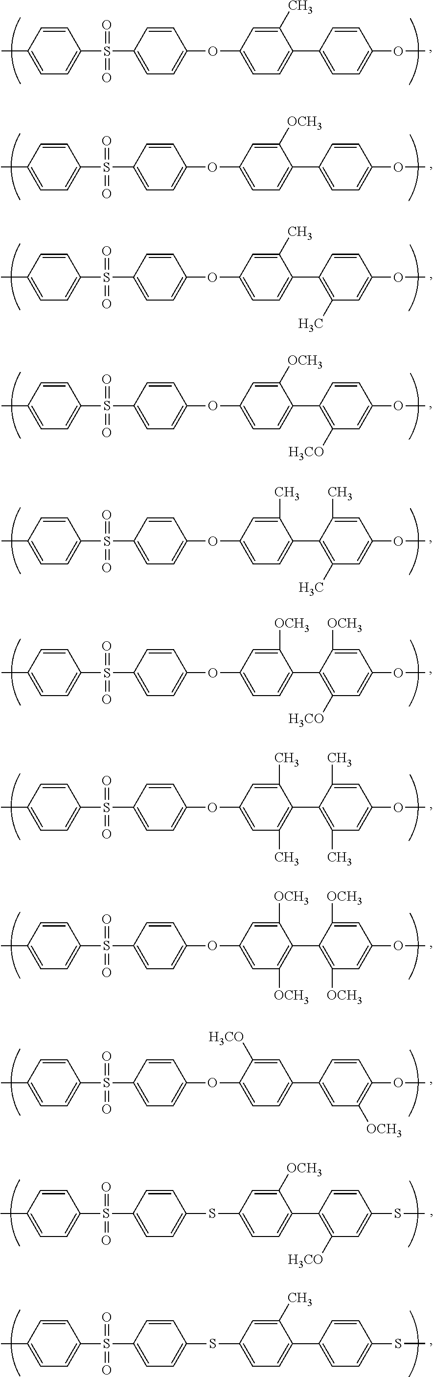


wherein:
L, at each occurrence, independently can be selected from the group consisting of —O—, —S—, a divalent C1-10 alkyl group, a divalent C6-18 aryl group, and a covalent bond;
T, at each occurrence, can be Q or R, wherein Q is a crosslinkable group;
p is 1, 2, 3 or 4;
and R, W, Z and Z′ are as defined herein, provided, for example, that at least one of the -L-T groups is an -L-Q group.

where m′ represents the mole fraction of the repeat unit in the polymer backbone having the unreacted -L-R group and can be as high as about 0.75 and as low as about 0 (100% conversion).


where R1 is H, F, CN, a C1-10 alkyl group, a C1-10 haloalkyl group, and a C1-10 alkoxy group.

wherein:
L′, at each occurrence, independently can be selected from the group consisting of —O—, —S—, a divalent C1-10 alkyl group, a divalent C6-18 aryl group, and a covalent bond;
T′, at each occurrence, independently can be Q or R, wherein:
-
- Q is a crosslinkable group; and
- R, at each occurrence, is selected from the group consisting of H, a halogen, a C1-10 alkyl group, a C1-10 haloalkyl group, and a C6-10 aryl group optionally substituted with 1 to 5 substituents independently selected from the group consisting of a halogen and CN; and
p′ is 1, 2, 3 or 4.


where R1 is H, F, CN, a C1-10 alkyl group, a C1-10 haloalkyl group, and a C1-10 alkoxy group.

where n′ represents the mole fraction of the repeat unit in the polymer backbone having the unreacted -L′-R group and can be as high as about 0.75 and as low as about 0 (100% conversion).

where m and n are real numbers representing mole fractions, provided that the sum of m and n is about 1. For example, each of m and n can be less than 1 but greater than 0 (i.e., 0<m<1 and 0<n<1), preferably, each of m and n is less than or equal to 0.9 but greater than or equal to 0.1 (i.e., 0.1≦m≦0.9 and 0.1≦n≦0.9), more preferably, each of m and n is less than or equal to 0.8 but greater than or equal to 0.2 (i.e., 0.2≦m≦0.8 and 0.2≦n≦0.8), even more preferably, each of m and n is less than or equal to 0.7 but greater than or equal to 0.3 (i.e., 0.3≦m≦0.7 and 0.3≦n≦0.7). In certain embodiments, n can be greater than m (i.e., n>m, provided that m+n=1. For example, m can be about 0.4, and n can be about 0.6; or m can be about 0.3, and n can be about 0.7; or m can be about 0.2, and n can be about 0.8; or m can be about 0.1, and n can be about 0.9. Embodiments of the present copolymers having a higher mole fraction of the second repeat unit of formula (IV) than the first repeat unit of formula (II) can be more thermally stable and more chemically resistant (for example, against etchants and/or strippers used with various commercially available positive or negative photoresists) than those copolymers where n is either the same or less than m.

where L, L′, R, W, Z and Z′ are as defined herein, but provided that at least one -L-R group or at least one -L′-R group is not H; p and p′ independently are 1, 2, 3 or 4; and m and n are real numbers representing mole fractions, provided that each of m and n can be less than 1 but greater than 0 (i.e., 0<m<1 and 0<n<1) and the sum of m and n is about 1. For example, the benzimidazolonyl group can be substituted with an -L′-R group and the polysulfone copolymer can be represented by the formula:

where L′, R, W, m and n are as defined herein, provided that L′ is not a covalent bond when R is H. As another example, W can include one or more Ar groups substituted with 1, 2, 3 or 4 -L-R groups and the polysulfone copolymer can be represented by the formula:

where L, R, W, m, n, and p are as defined herein, provided that L is not a covalent bond when R is H. As yet another example, both W and the benzimidazolonyl group can be substituted and the polysulfone copolymer can be represented by the formula:

where L, L′, R, W, m, n and p are as defined herein, provided that L and L′ do not represent a covalent bond when R is H. To illustrate, at least W and/or the benzimidazolonyl group can be substituted with 1-4 methoxy and/or methyl groups.

where L, L′, Q, R, W, Z, Z′ and p′ are as defined herein, each of m and n can be less than 1 but greater than 0 (i.e., 0<m<1 and 0<n<1) and the sum of m and n is about 1, and p is 1, 2 or 3. Where the reaction by which the crosslinkable group is attached to the polymer backbone can involve an -L-R group substituted on the W group, depending on the conversion rate of the reaction, certain embodiments in which the polysulfone copolymer includes a W group substituted with one or more crosslinkable groups can be represented by:

where L, L′, Q, R, W, Z, Z′ and p′ are as defined herein, each of m and n can be less than 1 but greater than 0 (i.e., 0<m<1 and 0<n<1) and the sum of m and n is about 1, p is 1, 2 or 3, and m′ represents the mole fraction of the repeat unit in the polymer backbone having the unreacted -L-R group and can be as high as about 0.75 and as low as about 0 (100% conversion). Similarly, embodiments of copolymers having the benzimidazolonyl group substituted with one or more crosslinkable groups can be represented by the formula:

where L, L′, Q, R, W, Z, Z′ and p are as defined herein, and each of m and n can be less than 1 but greater than 0 (i.e., 0<m<1 and 0<n<1) and the sum of m and n is about 1. Where the reaction by which the crosslinkable group is attached to the polymer backbone can involve an -L′-R group substituted on the benzimidazolonyl group, depending on the conversion rate of the reaction, the polysulfone copolymer can be represented by:

where L, L′, Q, R, W, Z, Z′ and p are as defined herein, each of m and n can be less than 1 but greater than 0 (i.e., 0<m<1 and 0<n<1) and the sum of m and n is about 1, and n′ represents the mole fraction of the repeat unit in the polymer backbone having the unreacted -L′-R group and can be as high as about 0.75 and as low as about 0 (100% conversion).

where L, L′, Q, R, W, Z and Z′ are as defined herein, each of m and n can be less than 1 but greater than 0 (i.e., 0<m<1 and 0<n<1) and the sum of m and n is about 1, and p is 1, 2 or 3. Where the reaction by which the crosslinkable group is attached to the polymer backbone can involve an -L-R group substituted on the W group and/or an -L′-R group substituted on the benzimidazolonyl group, depending on the conversion rate of the reaction, the polysulfone copolymer can be represented by the formula:

where L, L′, Q, R, W, Z and Z′ are as defined herein, each of m and n can be less than 1 but greater than 0 (i.e., 0<m<1 and 0<n<1) and the sum of m and n is about 1, p is 1, 2 or 3, and m′ and n′ represent the mole fraction of the repeat unit in the polymer backbone having the unreacted -L-R group and the mole fraction of the repeat unit in the polymer backbone having the unreacted -L′-R group, respectively, and can be as high as about 0.75 and as low as about 0 (100% conversion).

wherein:
L and L′, at each occurrence, independently can be selected from the group consisting of —O—, —S—, a divalent C1-10 alkyl group, a divalent C6-18 aryl group, and a covalent bond;
T and T′, at each occurrence, independently can be Q or R, wherein:
-
- Q is a crosslinkable group; and
- R, at each occurrence, is selected from the group consisting of H, a halogen, a C1-10 alkyl group, a C1-10 haloalkyl group, and a C6-10 aryl group optionally substituted with 1 to 5 substituents independently selected from the group consisting of a halogen and CN;
W can be —Ar[—Y—Ar]q—, wherein: - Ar, at each occurrence, independently can be a divalent C6-18 aryl group;
- Y, at each occurrence, independently can be selected from the group consisting of —O—, —S—, —(CR′R″)r—, —C(O)—, and a covalent bond, wherein R′ and R″, at each occurrence, independently can be selected from the group consisting of H, a halogen, CN, a C1-10 alkyl group, and a C1-10 haloalkyl group; and r is selected from the group consisting of 1, 2, 3, 4, 5, 6, 7, 8, 9 and 10; and
- q is selected from the group consisting of 0, 1, 2, 3, 4, 5, 6, 7, 8, 9 and 10;
Z and Z′ independently can be selected from the group consisting of —O—, —S—, and —Se—;
p and p′ independently are 1, 2, 3 or 4; and
m and n are real numbers representing mole fractions, wherein 0≦m≦1 and 0≦n≦1, provided that the sum of m and n is about 1.

where each X can be a leaving group such as a halogen (F, Cl, Br, I), CN, OTf, OMs, or NO2. In certain cases, transition metal-based catalysts, such as those of Pd or Ni, for promoting C—Z bond formation can be used. See Frlan, R. Kikelj, D. “Recent Progress in Diaryl Ether Synthesis,” Synthesis, 14: 2271-2285 (2006); Aubin, Y. et al., “Direct Amination of Aryl Halides with Ammonia,” Chemical Society Reviews, 39(11): 4130-4145 (2010); and Hassan, J. et al., “Aryl-Aryl Bond Formation One Century After the Discovery of the Ullmann Reaction,” Chemical Reviews, 102(5): 1359-1469 (2002). In addition, a could be equal to m and b could be equal to n depending on the relative reactivity of Z versus the N nucleophiles. In any case, m+n=1.

For example, -L-G can be an ether, e.g., —OMe, which can be dealkylated into OH (see Examples 3 and 11, infra), which in turn can be reacted with a compound bearing a crosslinkable moiety to provide -L-Q (
which could be used in Scheme 1, where L is a covalent bond and T is H include:


which could be used in Scheme 1 or Scheme 2, where L is —O— or a covalent bond and T is a methyl group (Me) include:

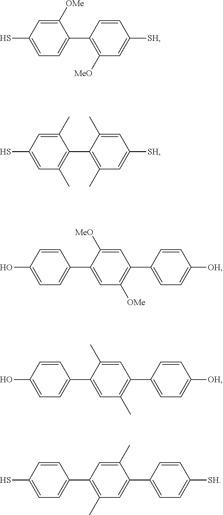


can be synthesized according to reported protocols for synthesizing the commercially available

such as:


where m and n are real numbers representing mole fractions, wherein 0<m<1 and 0<n<1, and the sum of m and n is about 1.

wherein:
L and L′, at each occurrence, independently can be selected from the group consisting of —O—, —S—, a divalent C1-10 alkyl group, a divalent C6-18 aryl group, and a covalent bond;
T and T′, at each occurrence, independently can be Q or R, wherein:
-
- Q is a crosslinkable group; and
- R, at each occurrence, is selected from the group consisting of H, a C1-10 alkyl group, a C1-10 haloalkyl group, and a C6-10 aryl group optionally substituted with 1 to 5 substituents independently selected from the group consisting of a halogen and CN;
W can be —Ar[—Y—Ar]q—, wherein: - Ar, at each occurrence, independently can be a divalent C6-18 aryl group;
- Y, at each occurrence, independently can be selected from the group consisting of —O—, —S—, —(CR′R″)r—, —C(O)—, and a covalent bond, wherein R′ and R″, at each occurrence, independently can be selected from the group consisting of H, a halogen, CN, a C1-10 alkyl group, and a C1-10 haloalkyl group; and r is selected from the group consisting of 1, 2, 3, 4, 5, 6, 7, 8, 9 and 10; and
- q is selected from the group consisting of 0, 1, 2, 3, 4, 5, 6, 7, 8, 9 and 10;
Z and Z′ independently can be selected from the group consisting of —O—, —S—, and —Se—;
p and p′ independently are 1, 2, 3 or 4;
m and n are real numbers representing mole fractions, wherein 0<m<1 and 0<n<1, and the sum of m and n is about 1; and
provided that at least one -L-T group is an -L-Q group, and/or at least one -L′-T group is an -L′-Q group. For example, p and/or p′ can be 1, and -L-T and/or -L′-T can be Q or —O— Q.

wherein:
L and L′, at each occurrence, independently can be selected from the group consisting of —O—, —S—, a divalent C1-10 alkyl group, a divalent C6-18 aryl group, and a covalent bond;
T and T′, at each occurrence, independently can be Q or R, wherein:
-
- Q is a crosslinkable group; and
- R, at each occurrence, is selected from the group consisting of H, a C1-10 alkyl group, a C1-10 haloalkyl group, and a C6-10 aryl group optionally substituted with 1 to 5 substituents independently selected from the group consisting of a halogen and CN;
W can be a divalent phenyl group;
Z and Z′ independently can be selected from the group consisting of —O—, —S—, and —Se—;
p and p′ independently are 1, 2, 3 or 4;
m and n are real numbers representing mole fractions, wherein 0<m<1 and 0<n<1, and the sum of m and n is about 1; and
provided that at least one -L-T group and/or at least one -L′-T group is not H. For example, p and/or p′ can be 1, and -L-T and/or -L′-T can be OMe, —O— Q, or Q.


where Func can be selected from the group consisting of:


where R1 is H, F, CN, a C1-10 alkyl group, a C1-10 haloalkyl group, and a C1-10 alkoxy group.


and/or a small molecule crosslinker such as:


or a diglycidyl ether polymer such as:


such polysulfones can be thermally crosslinked without any auxiliary reagents or with another compound (small molecule or polymer) having a double or triple-bond containing crosslinkable group. These polysulfones also can be cured via reaction with thiol (e.g., thiol-ene photopolymerization).

Poly[4,5-difluoro-2,2-bis(trifluoromethyl)-1,3-dioxole-co-tetrafluoroethylene (commercially available under the trade name Teflon® AF 2400) having the following structure also can be used:


| TABLE 1 |
| Dielectric properties of various polysulfone-based films. |
| PVP, PMMA, PBI and PEI films are included for comparison. |
| Bake 120° C., 10 min | Bake 250° C., 1 | Bake | 300° C., 1 h |
| Polymeric | J (A/cm2) | Ci | t | J (A/cm2) | Ci | t | J (A/cm2) | Ci | t |
| Insulator | at 2 MV/cm | (nF/cm2) | (nm) | at 2 MV/cm | (nF/cm2) | (nm) | at 2 MV/cm | (nF/cm2) | (nm) |
| PSECy (4k) | 1 × 10⁻⁸ | 5.2 | 630 | 2 × 10⁻⁸ | 6.1 | 550 | 2 × 10⁻⁸ | 6.8 | 500 |
| PSECy (10k) | 3 × 10⁻⁹ | 6.5 | 500 | 3 × 10⁻⁹ | 6.8 | 470 | 1 × 10⁻⁹ | 6.9 | 450 |
| PSA0.1E0.9Cy | 9 × 10⁻¹⁰ | 5.9 | 510 | 2 × 10⁻⁹ | 6.2 | 500 | 2 × 10⁻⁹ | 6.3 | 500 |
| PSA0.3E0.7Cy | 4 × 10⁻⁹ | 6.0 | 550 | 8 × 10⁻¹⁰ | 6.1 | 520 | 6 × 10⁻⁷ | 6.0 | 520 |
| PSA0.4E0.6Cy | 9 × 10⁻⁹ | 6.0 | 520 | 9 × 10⁻⁹ | 6.3 | 510 | 1 × 10⁻⁷ | 6.6 | 480 |
| |
6 × 10⁻⁷ | 6.5 | 570 | Film damaged | Film damaged |
| PMMA | 7 × 10⁻⁹ | 12 | 250 | Film damaged | Film damaged |
| |
1 × 10⁻⁹ | 7.6 | 440 | 1 × 10⁻⁶ | 8.4 | 390 | |||
| |
1 × 10⁻⁸ | 6.6 | 490 | 1 × 10⁻⁸ | 6.6 | 470 | |||
| TABLE 2 |
| Device performance of IGZO TFTs incorporating a polysulfone-based |
| gate dielectric. Carrier mobility was calculated in saturation. |
| μ | Gate leakage | |||
| Gate dielectric polymer | Substrate | (cm2/VS) | Ion:Ioff | (nA) |
| PSA0.1E0.9Cy | Si | 8.4 | 105 | 0.1 |
| PSA0.3E0.7Cy | Si | 9.5 | 106 | 0.01 |
| PSECy | Si | 6.9 | 103 | 1 |
| PEI | Si | N/A | N/A | N/A |
| TABLE 3 |
| Device performance of IGZO TFTs incorporating a polysulfone-based passivation |
| layer and control devices without a passivation layer. Carrier mobility was calculated in |
| saturation, PBTS applied at 80° C., VGS = 30 V and VDS = 0 V for 1500 seconds. |
| |
| Mobility | Von | Hysteresis | Von PBTS | Von PBTS | |
| Passivation Layer | (cm2/Vs) | (V) | (V) | shift (V) | shift (V) |
| No passivation | 8.2 | −0.5 | 1.5 | 8 | 4.5 ~ 6.5 |
| No passivation (tested in vacuum) | 8.9 | −0.5 | 0 | 1 | |
| PSA0.1E0.9Cy | 8.1 | −1 | 1 | 1.5 ~ 6 | 1 ~ 2.5 |
| PSA0.3E0.7Cy | 8.8 | −2 | 0.5 | 0.5 ~ 5 | 0.5 ~ 5 |
| PSA0.3E0.7Cy: cinnamoyl- | 8.7 | −4 | 1 | −1 ~ −2 | 0 ~ 2.5 |
| modified PMMA (8:2) blend | |||||
Claims (20)


Priority Applications (1)
| Application Number | Priority Date | Filing Date | Title |
|---|---|---|---|
| US13/844,129 US9035287B2 (en) | 2013-02-01 | 2013-03-15 | Polymeric materials for use in metal-oxide-semiconductor field-effect transistors |
Applications Claiming Priority (2)
| Application Number | Priority Date | Filing Date | Title |
|---|---|---|---|
| US201361759406P | 2013-02-01 | 2013-02-01 | |
| US13/844,129 US9035287B2 (en) | 2013-02-01 | 2013-03-15 | Polymeric materials for use in metal-oxide-semiconductor field-effect transistors |
Publications (2)
| Publication Number | Publication Date |
|---|---|
| US20140217395A1 US20140217395A1 (en) | 2014-08-07 |
| US9035287B2 true US9035287B2 (en) | 2015-05-19 |
Family
ID=51258544
Family Applications (1)
| Application Number | Title | Priority Date | Filing Date |
|---|---|---|---|
| US13/844,129 Active 2033-11-30 US9035287B2 (en) | 2013-02-01 | 2013-03-15 | Polymeric materials for use in metal-oxide-semiconductor field-effect transistors |
Country Status (1)
| Country | Link |
|---|---|
| US (1) | US9035287B2 (en) |
Cited By (3)
| Publication number | Priority date | Publication date | Assignee | Title |
|---|---|---|---|---|
| US20150279671A1 (en) * | 2014-03-28 | 2015-10-01 | Industry-Academic Cooperation Foundation, Yonsei University | Method for forming oxide thin film and method for fabricating oxide thin film transistor employing germanium doping |
| WO2016065276A1 (en) | 2014-10-24 | 2016-04-28 | Polyera Corporation | Photopatternable compositions and methods of fabricating transistor devices using same |
| US10158078B2 (en) | 2016-05-12 | 2018-12-18 | Korea Research Institute Of Chemical Technology | Composition for insulator of thin film transistor, insulator and organic thin film transistor prepared thereby |
Families Citing this family (10)
| Publication number | Priority date | Publication date | Assignee | Title |
|---|---|---|---|---|
| KR101947166B1 (en) * | 2012-11-19 | 2019-02-13 | 삼성디스플레이 주식회사 | Substrate and display device including the same |
| JP6394171B2 (en) | 2013-10-30 | 2018-09-26 | 株式会社リコー | Field effect transistor, display element, image display device, and system |
| US9391210B2 (en) * | 2014-09-16 | 2016-07-12 | Eastman Kodak Company | Top gate TFT with polymer interface control layer |
| GB201418610D0 (en) * | 2014-10-20 | 2014-12-03 | Cambridge Entpr Ltd | Transistor devices |
| WO2016072455A1 (en) * | 2014-11-07 | 2016-05-12 | 富士フイルム株式会社 | Organic semiconductor element and compound |
| US9887277B2 (en) * | 2015-01-23 | 2018-02-06 | Applied Materials, Inc. | Plasma treatment on metal-oxide TFT |
| CN104795496A (en) * | 2015-04-08 | 2015-07-22 | 深圳市华星光电技术有限公司 | Bigrid device and manufacturing method thereof |
| US9904171B2 (en) * | 2015-05-22 | 2018-02-27 | I-Shan Ke | Resist pattern hardening material and method of fabricating the same |
| KR101807454B1 (en) | 2015-06-26 | 2017-12-08 | 사빅 글로벌 테크놀러지스 비.브이. | Integrated piezoelectric cantilever actuator and transistor for touch input and haptic feedback applications |
| US20200006412A1 (en) * | 2018-06-28 | 2020-01-02 | Applied Materials, Inc. | Methods and apparatus for image sensor semiconductors |
Citations (16)
| Publication number | Priority date | Publication date | Assignee | Title |
|---|---|---|---|---|
| US4837256A (en) | 1983-06-13 | 1989-06-06 | Amoco Corporation | Crosslinkable, crystallizable polyarylethers and composites therefrom |
| US20050065278A1 (en) | 2003-09-19 | 2005-03-24 | Mercado Ramil-Marcelo L. | Polyimides for use as high refractive index, thin film materials |
| US20060155096A1 (en) | 2002-09-20 | 2006-07-13 | Shinsuke Matsumoto | Thermoplastic polymer, thermoplastic polymer composition, antistatic agent, and resin composition |
| US20080067503A1 (en) * | 2006-09-15 | 2008-03-20 | Joo Young Kim | Insulating organic polymer, organic insulating layer formed using the insulating polymer, and organic thin film transistor comprising the insulating layer |
| US20080081205A1 (en) | 2006-09-29 | 2008-04-03 | Fujifilm Corporation | Gas-barrier laminate film and image display device comprising same |
| US20080161524A1 (en) * | 2006-11-28 | 2008-07-03 | He Yan | Photopolymer-based dielectric materials and methods of preparation and use thereof |
| US7696298B2 (en) | 2007-09-07 | 2010-04-13 | Hay Allan S | Poly(arylenebenzimidazole) polymers and copolymers |
| JP2010108986A (en) | 2008-10-28 | 2010-05-13 | Hitachi Chem Co Ltd | Material forming gate insulating film layer, field effect transistor and process for fabricating field effect transistor |
| US20100234479A1 (en) | 2005-09-30 | 2010-09-16 | Battelle Memorial Insititute | Polymers for Use in Fuel Cell Components |
| US20100237337A1 (en) * | 2007-09-27 | 2010-09-23 | Masakazu Kamura | Organic transistor and method for producing the same |
| US20100252112A1 (en) * | 2009-04-06 | 2010-10-07 | Watson Mark D | Semiconducting Compounds and Devices Incorporating Same |
| WO2010136385A1 (en) * | 2009-05-25 | 2010-12-02 | Basf Se | Crosslinkable dielectrics and methods of preparation and use thereof |
| US20110180784A1 (en) * | 2010-01-22 | 2011-07-28 | Deepak Shukla | Organic semiconducting compositions and n-type semiconductor devices |
| US20110284849A1 (en) * | 2010-05-19 | 2011-11-24 | Marks Tobin J | Crosslinked Hybrid Gate Dielectric Materials and Electronic Devices Incorporating Same |
| US20120056183A1 (en) * | 2010-09-02 | 2012-03-08 | Promerus Llc | Gate insulator layer for organic electronic devices |
| US20120267621A1 (en) * | 2011-04-22 | 2012-10-25 | Au Optronics Corporation | Thin film transistor and fabrication method thereof |
-
2013
- 2013-03-15 US US13/844,129 patent/US9035287B2/en active Active
Patent Citations (16)
| Publication number | Priority date | Publication date | Assignee | Title |
|---|---|---|---|---|
| US4837256A (en) | 1983-06-13 | 1989-06-06 | Amoco Corporation | Crosslinkable, crystallizable polyarylethers and composites therefrom |
| US20060155096A1 (en) | 2002-09-20 | 2006-07-13 | Shinsuke Matsumoto | Thermoplastic polymer, thermoplastic polymer composition, antistatic agent, and resin composition |
| US20050065278A1 (en) | 2003-09-19 | 2005-03-24 | Mercado Ramil-Marcelo L. | Polyimides for use as high refractive index, thin film materials |
| US20100234479A1 (en) | 2005-09-30 | 2010-09-16 | Battelle Memorial Insititute | Polymers for Use in Fuel Cell Components |
| US20080067503A1 (en) * | 2006-09-15 | 2008-03-20 | Joo Young Kim | Insulating organic polymer, organic insulating layer formed using the insulating polymer, and organic thin film transistor comprising the insulating layer |
| US20080081205A1 (en) | 2006-09-29 | 2008-04-03 | Fujifilm Corporation | Gas-barrier laminate film and image display device comprising same |
| US20080161524A1 (en) * | 2006-11-28 | 2008-07-03 | He Yan | Photopolymer-based dielectric materials and methods of preparation and use thereof |
| US7696298B2 (en) | 2007-09-07 | 2010-04-13 | Hay Allan S | Poly(arylenebenzimidazole) polymers and copolymers |
| US20100237337A1 (en) * | 2007-09-27 | 2010-09-23 | Masakazu Kamura | Organic transistor and method for producing the same |
| JP2010108986A (en) | 2008-10-28 | 2010-05-13 | Hitachi Chem Co Ltd | Material forming gate insulating film layer, field effect transistor and process for fabricating field effect transistor |
| US20100252112A1 (en) * | 2009-04-06 | 2010-10-07 | Watson Mark D | Semiconducting Compounds and Devices Incorporating Same |
| WO2010136385A1 (en) * | 2009-05-25 | 2010-12-02 | Basf Se | Crosslinkable dielectrics and methods of preparation and use thereof |
| US20110180784A1 (en) * | 2010-01-22 | 2011-07-28 | Deepak Shukla | Organic semiconducting compositions and n-type semiconductor devices |
| US20110284849A1 (en) * | 2010-05-19 | 2011-11-24 | Marks Tobin J | Crosslinked Hybrid Gate Dielectric Materials and Electronic Devices Incorporating Same |
| US20120056183A1 (en) * | 2010-09-02 | 2012-03-08 | Promerus Llc | Gate insulator layer for organic electronic devices |
| US20120267621A1 (en) * | 2011-04-22 | 2012-10-25 | Au Optronics Corporation | Thin film transistor and fabrication method thereof |
Cited By (3)
| Publication number | Priority date | Publication date | Assignee | Title |
|---|---|---|---|---|
| US20150279671A1 (en) * | 2014-03-28 | 2015-10-01 | Industry-Academic Cooperation Foundation, Yonsei University | Method for forming oxide thin film and method for fabricating oxide thin film transistor employing germanium doping |
| WO2016065276A1 (en) | 2014-10-24 | 2016-04-28 | Polyera Corporation | Photopatternable compositions and methods of fabricating transistor devices using same |
| US10158078B2 (en) | 2016-05-12 | 2018-12-18 | Korea Research Institute Of Chemical Technology | Composition for insulator of thin film transistor, insulator and organic thin film transistor prepared thereby |
Also Published As
| Publication number | Publication date |
|---|---|
| US20140217395A1 (en) | 2014-08-07 |
Similar Documents
| Publication | Publication Date | Title |
|---|---|---|
| US9035287B2 (en) | Polymeric materials for use in metal-oxide-semiconductor field-effect transistors | |
| US8878169B2 (en) | Photocurable polymeric materials and related electronic devices | |
| US9704997B2 (en) | Photopatternable materials and related electronic devices and methods | |
| US9929345B1 (en) | Curable polymeric materials and their use for fabricating electronic devices | |
| US9923158B2 (en) | Photocurable polymeric dielectrics and methods of preparation and use thereof | |
| EP1629544B1 (en) | Polymer transistor | |
| US8338555B2 (en) | Photopolymers and their use in organic thin film transistors | |
| US20080315192A1 (en) | Integrated Circuit Comprising an Organic Semiconductor, and Method for the Production of an Integrated Circuit | |
| US20160204350A1 (en) | Polymyeric organic semiconductor compositions | |
| US10147895B2 (en) | Curable polymeric materials and their use for fabricating electronic devices | |
| EP2812931B1 (en) | Electronic devices comprising photocurable polymeric materials | |
| US11345778B2 (en) | Organic dielectric materials and devices including them | |
| US8692238B2 (en) | Semiconductor devices and methods of preparation | |
| EP2063471B1 (en) | Organic field effect transistor |
Legal Events
| Date | Code | Title | Description |
|---|---|---|---|
| AS | Assignment |
Owner name: POLYERA CORPORATION, ILLINOIS Free format text: ASSIGNMENT OF ASSIGNORS INTEREST;ASSIGNORS:FACCHETTI, ANTONIO;BATZEL, DANIEL;CHEN, JING;AND OTHERS;SIGNING DATES FROM 20130617 TO 20130815;REEL/FRAME:034816/0105 |
|
| STCF | Information on status: patent grant |
Free format text: PATENTED CASE |
|
| AS | Assignment |
Owner name: FLEXTERRA, INC., ILLINOIS Free format text: ASSIGNMENT OF ASSIGNORS INTEREST;ASSIGNOR:POLYERA CORPORATION;REEL/FRAME:041197/0650 Effective date: 20161221 |
|
| FEPP | Fee payment procedure |
Free format text: ENTITY STATUS SET TO UNDISCOUNTED (ORIGINAL EVENT CODE: BIG.) |
|
| MAFP | Maintenance fee payment |
Free format text: PAYMENT OF MAINTENANCE FEE, 4TH YEAR, LARGE ENTITY (ORIGINAL EVENT CODE: M1551); ENTITY STATUS OF PATENT OWNER: LARGE ENTITY Year of fee payment: 4 |
|
| AS | Assignment |
Owner name: SAES GETTERS INTERNATIONAL LUXEMBOURG S.A., IN ITS CAPACITY AS COLLATERAL AGENT, LUXEMBOURG Free format text: SECURITY INTEREST;ASSIGNOR:FLEXTERRA, INC.;REEL/FRAME:058226/0591 Effective date: 20200716 |
|
| MAFP | Maintenance fee payment |
Free format text: PAYMENT OF MAINTENANCE FEE, 8TH YEAR, LARGE ENTITY (ORIGINAL EVENT CODE: M1552); ENTITY STATUS OF PATENT OWNER: LARGE ENTITY Year of fee payment: 8 |