US9065452B1 - Superconducting digital phase rotator - Google Patents

Superconducting digital phase rotator Download PDF

Info

Publication number
US9065452B1
US9065452B1 US13/073,942 US201113073942A US9065452B1 US 9065452 B1 US9065452 B1 US 9065452B1 US 201113073942 A US201113073942 A US 201113073942A US 9065452 B1 US9065452 B1 US 9065452B1
Authority
US
United States
Prior art keywords
phase
signal
clock
input signal
digital
Prior art date
Legal status (The legal status is an assumption and is not a legal conclusion. Google has not performed a legal analysis and makes no representation as to the accuracy of the status listed.)
Active, expires
Application number
US13/073,942
Inventor
Amol Ashok Inamdar
Current Assignee (The listed assignees may be inaccurate. Google has not performed a legal analysis and makes no representation or warranty as to the accuracy of the list.)
Hypres Inc
Original Assignee
Hypres Inc
Priority date (The priority date is an assumption and is not a legal conclusion. Google has not performed a legal analysis and makes no representation as to the accuracy of the date listed.)
Filing date
Publication date
Application filed by Hypres Inc filed Critical Hypres Inc
Priority to US13/073,942 priority Critical patent/US9065452B1/en
Priority to US14/743,409 priority patent/US9344069B1/en
Application granted granted Critical
Publication of US9065452B1 publication Critical patent/US9065452B1/en
Priority to US15/155,687 priority patent/US9748937B1/en
Priority to US15/687,020 priority patent/US10355681B1/en
Assigned to AVIDBANK reassignment AVIDBANK SECURITY INTEREST (SEE DOCUMENT FOR DETAILS). Assignors: HYPRES, INC.
Active legal-status Critical Current
Adjusted expiration legal-status Critical

Links

Images

Classifications

    • HELECTRICITY
    • H03ELECTRONIC CIRCUITRY
    • H03KPULSE TECHNIQUE
    • H03K5/00Manipulating of pulses not covered by one of the other main groups of this subclass
    • H03K5/13Arrangements having a single output and transforming input signals into pulses delivered at desired time intervals
    • H03K5/131Digitally controlled
    • HELECTRICITY
    • H03ELECTRONIC CIRCUITRY
    • H03LAUTOMATIC CONTROL, STARTING, SYNCHRONISATION, OR STABILISATION OF GENERATORS OF ELECTRONIC OSCILLATIONS OR PULSES
    • H03L7/00Automatic control of frequency or phase; Synchronisation
    • H03L7/06Automatic control of frequency or phase; Synchronisation using a reference signal applied to a frequency- or phase-locked loop
    • H03L7/08Details of the phase-locked loop
    • H03L7/0805Details of the phase-locked loop the loop being adapted to provide an additional control signal for use outside the loop
    • HELECTRICITY
    • H03ELECTRONIC CIRCUITRY
    • H03KPULSE TECHNIQUE
    • H03K3/00Circuits for generating electric pulses; Monostable, bistable or multistable circuits
    • H03K3/02Generators characterised by the type of circuit or by the means used for producing pulses
    • H03K3/38Generators characterised by the type of circuit or by the means used for producing pulses by the use, as active elements, of superconductive devices
    • HELECTRICITY
    • H03ELECTRONIC CIRCUITRY
    • H03KPULSE TECHNIQUE
    • H03K5/00Manipulating of pulses not covered by one of the other main groups of this subclass
    • H03K5/13Arrangements having a single output and transforming input signals into pulses delivered at desired time intervals
    • HELECTRICITY
    • H03ELECTRONIC CIRCUITRY
    • H03LAUTOMATIC CONTROL, STARTING, SYNCHRONISATION, OR STABILISATION OF GENERATORS OF ELECTRONIC OSCILLATIONS OR PULSES
    • H03L7/00Automatic control of frequency or phase; Synchronisation
    • H03L7/06Automatic control of frequency or phase; Synchronisation using a reference signal applied to a frequency- or phase-locked loop
    • H03L7/08Details of the phase-locked loop
    • H03L7/081Details of the phase-locked loop provided with an additional controlled phase shifter
    • H03L7/0812Details of the phase-locked loop provided with an additional controlled phase shifter and where no voltage or current controlled oscillator is used
    • H03L7/0814Details of the phase-locked loop provided with an additional controlled phase shifter and where no voltage or current controlled oscillator is used the phase shifting device being digitally controlled
    • HELECTRICITY
    • H03ELECTRONIC CIRCUITRY
    • H03LAUTOMATIC CONTROL, STARTING, SYNCHRONISATION, OR STABILISATION OF GENERATORS OF ELECTRONIC OSCILLATIONS OR PULSES
    • H03L7/00Automatic control of frequency or phase; Synchronisation
    • H03L7/06Automatic control of frequency or phase; Synchronisation using a reference signal applied to a frequency- or phase-locked loop
    • H03L7/16Indirect frequency synthesis, i.e. generating a desired one of a number of predetermined frequencies using a frequency- or phase-locked loop
    • HELECTRICITY
    • H03ELECTRONIC CIRCUITRY
    • H03KPULSE TECHNIQUE
    • H03K5/00Manipulating of pulses not covered by one of the other main groups of this subclass
    • H03K2005/00286Phase shifter, i.e. the delay between the output and input pulse is dependent on the frequency, and such that a phase difference is obtained independent of the frequency

Definitions

  • the field of the invention relates to superconducting digital integrated circuits and, more particularly, to a digital phase rotator which permits phase shifts in a positive and negative direction.
  • High-speed digital circuits are generally synchronous, with a periodic clock signal distributed throughout the circuit.
  • a multi-phase clock signal may be used, with two or more clock signals distributed in parallel.
  • a two-phase clock may have one clock signal delayed one-half a clock period with respect to the second clock signal.
  • a circuit optimized for this purpose is often called a phase-delay generator or simply a phase generator.
  • phase rotator or sometimes a phase interpolator
  • a generic phase rotator or phase generator can be represented by the same block diagram of FIG. 1 . This shows a master clock input, one or more phase-shifted clock outputs, and a control input. The control input may in general be an analog signal, but the focus of the invention described herein is on a digital control input signal.
  • phase generators and phase rotators have been developed in standard semiconductor circuit technologies, and are examples of the prior art.
  • clock refers to a generally periodic sequence of pulses.
  • a pulse train may have a broader range of applications than strictly serving as a clock in a synchronized circuit.
  • a pulse train can serve as a carrier in a digital modulation scheme.
  • clock does not restrict possible applications of a phase rotator or related circuits.
  • Ultrafast superconducting digital circuits are based on Josephson junctions integrated together according to RSFQ Logic (Rapid-single-flux-quantum), first proposed by K. Likharev and V. Semenov (1991). Multi-GHz clock rates are routine in this technology, with rates of 100 GHz or higher possible. These very high speeds enable precision timing circuits.
  • Earlier fast timing circuits include a time-to-digital converter (A. Kirichenko, et al., “RSFQ Time Digitizing System”, IEEE Trans. Appl. Supercond., vol. 1, 2001, pp. 978-981.), and a digital programmable phase generator (A. Kirichenko, S. Sarwana, D. Gupta and D.
  • the digital programmable phase generator shown in application Ser. No. 11/243,020 is shown in FIG. 2 .
  • This follows the model of FIG. 1 , with a high-frequency clock input, a decimated clock output, and a set of digital input bits that determine the delay of the output.
  • This is comprised of an alternating chain of m TFFs and m ⁇ 1 inverters, with the decimated clock a factor of 2 m slower than that of the master clock on the left.
  • the m ⁇ 1 control inputs represent the bits of a binary number N (the most significant bit is on the right), then the phase delay at the output is given by 360° ⁇ N/2 m .
  • This quantum linearity has enabled superconducting analog-to-digital converters (ADCs) that can directly digitize radio-frequency signals as shown in (O. Mukhanov, et al., “Superconducting Analog-to-Digital Converters”, Proceedings of the IEEE, vol. 92, 2004, pp. 1564-1584).
  • phase-modulation ADC One type of superconducting ADC is known as the phase-modulation ADC, in which the analog input signal is encoded in the modulated timing of a fast SFQ pulse train.
  • direct digital synthesis of RF signals essentially an RF digital-to-analog converter or DAC
  • DAC digital-to-analog converter
  • the prior art lacked a superconducting phase rotator, which allows phase to be adjusted in both positive and a negative direction. Further, this needs to be done at an ultra-fast rate utilizing RSFQ logic.
  • the invention described herein overcomes the problems of the prior art.
  • the present invention describes a fast digital phase rotator circuit, where a multi-phase clock signal can be phase-shifted at multi-GHz rates.
  • Preferred implementations of this circuit are shown in FIGS. 3A-3D , where the circuit is comprised of superconducting RSFQ elements, including TFFs, Confluence Buffers (CBs), inverters, and a latch.
  • a phase delay (decrement) or a phase advance (increment) can be synthesized.
  • This example is designed for a master clock of 32 GHz, and a decimated output clock of 2 GHz.
  • FIG. 3C is designed for a 4-phase clock.
  • the clock ratio and numbers of output phases may be easily modified by changing the number and configuration of TFF stages.
  • FIG. 7 shows the relative phase angles of each of the 4 clock outputs.
  • the phase may be modulated at a rate of 2 GHz, the same rate as the output clock. This is why this circuit is appropriate as a digital phase modulator for a fast DAC.
  • Such a phase rotator with multiple clock phases may also have application in generating a specially shaped output pulse, for equalization of high-speed digital amplifiers.
  • a plurality of simple phase rotators of FIG. 3A are cascaded together in a way that can achieve additional precision.
  • a precision to one part in 2 m can be obtained.
  • large m arbitrary precision can be achieved.
  • FIG. 1 is a block diagram of a generic phase rotator.
  • FIG. 2 is a block diagram of a digital programmable phase generator as shown in U.S. patent application Ser. No. 11/243,020.
  • FIG. 3A is a block diagram of a phase rotator with bipolar single-bit control inputs, in accordance with one aspect of the invention.
  • FIG. 3B is a block diagram of a phase rotator that cascades a plurality of bipolar single bit phase rotators, to form a multi-bit phase rotator with a binary-weighted control input.
  • FIG. 3C is a block diagram of a phase rotator of FIG. 3A followed by a frequency divider.
  • FIG. 3D is a block diagram of a phase rotator with a synchronizer front end to combine four equal-weighted control bits onto two bipolar control lines.
  • FIG. 4 is a block diagram of an exemplary synchronizing block shown in FIG. 3D .
  • FIG. 5 is a block diagram of an example of a circuit for generating the control signals of FIG. 3 .
  • FIG. 6 is a timing diagram for illustrating the states of the multiplexers of FIG. 4 .
  • FIG. 7 is a diagram representing discrete values of four output clock phases available from the phase rotator of FIG. 3D .
  • FIG. 8A is a graph showing test results from the phase rotator of FIG. 3D with no control inputs applied.
  • FIG. 8B is an exemplary layout of a phase rotator in accordance with one aspect of the invention.
  • FIG. 9 is a graph showing test results from the phase rotator of FIG. 3D with an increment pulses applied at 1/16th of the clock frequency.
  • FIG. 10 is a graph showing test results from the phase rotator of FIG. 3D with decrement pulses applied at 1/16th of the clock frequency.
  • FIG. 11A is a graph showing test results from the phase rotator of FIG. 3D with two decrement pulses applied at 1/16th of the clock frequency.
  • FIG. 11B is a graph showing test results from the phase rotator of FIG. 3D with two increment pulses applied at 1/16th of the clock frequency.
  • FIG. 13 shows the use of the phase rotator as part of a direct digital synthesizer.
  • FIG. 1 shows a block diagram of a generic phase rotator or phase generator that has a master clock input, one or more phase-shifted clock outputs, and a control input.
  • the control input may in general be an analog signal but the focus of this invention is on a digital control input signal.
  • the digital programmable phase generator of Kirichenko is described in pending patent application Ser. No. 11/243,020. As shown in FIG. 2 , the phase generator of Kirichenko was able to adjust phase only in a single direction and therefore lacked the flexibility of the present invention.
  • FIG. 3A is a block diagram of a phase rotator in accordance with one aspect of the invention with one control bit being a decrement input (DEC0) and one bit being an increment input (INC0).
  • the circuit comprises an inverter, toggle flip-flop (TFF), confluence buffer (CB) and latches.
  • a decrement input (DEC0) causes the inverter to delay one pulse interval, retarding the timing of the pulse stream by one master clock period.
  • an increment (INC0) input bypasses the first TFF to advance the timing of the output pulse stream by one clock period.
  • the phase of the output pulse stream can be shifted by one clock period in any direction.
  • the master clock is applied to a first inverter which is also connected to the DEC0 line.
  • a DEC0 pulse is present, the output of the inverter is stopped for the interval of a pulse and the decremented clock is then passed to a second inverter connected to the INC0 line.
  • the master clock With no INC0 or DEC0 pulses present, the master clock will pass through the inverters without change.
  • the INC0 pulse is present on the inverter connected to the INC0 line, the bypass line connected to the INC0 line and connecting to the a confluence buffer (CB) as shown will advance the timing of the output pulse stream by one master clock period.
  • CB confluence buffer
  • the DEC0 pulse will delay a pulse from the master clock train applied through the TFF to CB and the latch by one clock period and the INC0 pulse will advance the timing of the output pulse train by one clock period.
  • the latch is a type D flip-flop which insures that the pulses generated are synchronized to the master clock.
  • a similar clocked latch is included in the bypass line that leads from the INC0 line to the CB. where the clock input to this clocked latch may be provided by the output of the first inverter.
  • FIG. 3B is a block diagram of a phase rotator that cascades a plurality of single bit phase rotators, such as shown in FIG. 3A to form a multi-bit phase rotator.
  • Two multi-bit binary-weighted words INC, and DEC serve as digital input words specifying the amount of phase shift increment or decrement respectively.
  • the resultant shift in phase corresponds to the difference between the increment and decrement number.
  • N N INC ⁇ N DEC .
  • the bits of each digital word in FIG. 3B are related to the other as bits of a binary word that represent a number, whereas, in FIG. 3A and FIG.
  • the bits represent equal-weighted contributions to increment or decrement.
  • N m-bit binary number
  • One advantage of this generalized m-bit input is that the phase rotator can be made arbitrarily precise, if m is large enough.
  • FIG. 3C is a block diagram of a one bit phase rotator of FIG. 3A followed by a frequency divider to generate multiple phases of the output.
  • the number of TFFs in the frequency chain depends on the required output frequency. In the absence of increment or decrement input, the circuit decimates the master clock by a factor of 2 m , where m is a number of TFFs.
  • FIG. 3D is a block diagram of a phase rotator with a synchronizer-multiplexer front end.
  • Four control inputs namely DEC1, DEC2, INC1 and INC2 serve to control the phase shift. These inputs are applied to the synchronizing block SYNC which also receives an input from the master clock.
  • the SYNC block will be described more hereinafter in conjunction with FIG. 4 .
  • Two outputs, a DEC output and an INC output, serve to cause an incrementing of the clock or a decrementing of the clock as discussed more hereinafter.
  • the master clock is applied to an inverter which is also connected to the DEC line.
  • the output of the inverter is stopped for a pulse interval (master clock period) and the decremented clock is then passed to an inverter connected to the INC line.
  • the master clock With no INC or DEC pulses present, the master clock will pass through the inverters without change.
  • the INC pulse is present on the inverter connected to the INC line, the bypass line connected to the INC line and connecting to the confluence buffer (CB) as shown will advance a pulse into the output pulse train.
  • the DEC pulse will effectively delay a pulse from the master clock train applied through the TFF to the latch and the INC pulse will advance a pulse in that pulse train.
  • the latch is a type D flip-flop which insures that the pulses generated are synchronized to the master clock.
  • the circuit of FIG. 3D is designed for 4 parallel one bit inputs, two each for increment and decrement.
  • the two INC inputs have equal weights, which differs from a 2-binary-bit INC input (as in FIG. 3B ) where the most significant bit (MSB) would have twice the weight of the least significant bit (LSB).
  • the master clock operates at 32 GigaSamples per seconds (GS/s).
  • the 32 GS/s clock is applied to a first toggle flip-flop (TFF) which divides a clock rate down to 16 GS/s.
  • the first TFF after the latch, divides the master clock down to 8 GS/s and the subsequent TFF divides it down to 4 GS/s.
  • the 4 GS/s outputs are applied to respected toggle flip-flops which are fed by regular and inverted outputs from the 4 GS/s TFF, thus producing four output phases at 2 GS/s each with each of the phases from a particular output TFF being in quadrature relationship.
  • FIG. 4 is a block diagram of an exemplary synchronizing block SYNC shown in FIG. 3 .
  • a synchronizer block is optional, but does make the phase rotator work better by reducing phase jitter.
  • a master clock input 400 (e.g. operating at 32 GS/s) feeds a chain of dividers 410 and 420 , producing clock signals at 32 GS/sec, 16 GS/sec, 8 GS/sec and 4 GS/sec.
  • the last stage of the divider chain 420 produces regular and inverted outputs CLK ⁇ 1 and CLK ⁇ 2 each operating at 2 GS/s.
  • the clocks CLK ⁇ 1 and CLK ⁇ 2 are applied to RSFQ multiplexers 430 and 440 .
  • the inputs DEC1 and DEC2 are alternatively selected by the multiplexer and applied to the output line DEC.
  • input lines INC1 and INC2 are multiplexed and applied sequentially to the output line INC.
  • the DEC and the INC lines each have an output rate, in this example, at 4 GS/s.
  • a series of latches 450 i and 450 j receive the output of the multiplexer 430 and 440 respectively. These latches serve to synchronize the phase transitions of the multiplexer outputs to the 4 GS/sec, the 8 GS/sec, 16 GS/sec and 32 GS/sec clock signals produced by the chain of dividers.
  • a confluence buffer (CB) merges two input pulse streams into a single output pulse stream.
  • a confluence buffer has no protection for the case where two pulses come in at the same time—one of the two will be lost.
  • a proper multiplexer (MUX) provides for interleaving two input pulse streams together, using a two phase clock and latches to make sure that no pulses get lost. This is more complicated than a CB, but it is still a standard RSFQ circuit that is not the subject of the present invention.
  • the particular type of driver utilized depends upon the type of control input signal. If the input were analog, the driver could constitute a ⁇ modulator that applies increment and decrement pulses in response to changes in the input signal. If the control input were a digital input, the INC and DEC pulses could represent whether or not the state of the control input is above or below a threshold level for the digital control input word.
  • the particular type of driver is not important. Rather, the type of driver will vary depending upon the particular application to which the phase rotator is put.
  • the INC and DEC inputs can be simply digital signals generated by a digital signal processor. These INC and DEC inputs may be multi-bit, binary inputs, or else single-bit over-sampled inputs.
  • FIG. 6 is a timing diagram illustrating the windows during which multiplexers of FIG. 4 permit RSFQ pulses from the various input lines of FIG. 3D , for example, to pass to respective output lines DEC and INC.
  • the top timing line shows that the outputs of multiplexer 430 and 440 of FIG. 4 , alternately produces windows during which an output signal corresponding to DEC1 and DEC2 can be applied to the DEC output in a repeated fashion.
  • the lower timeline labeled INC shows the output from multiplexer 430 and 440 of FIG. 4 , which open windows that permit an alternating sequence of INC1 and INC2 signals to pass to the INC line output.
  • FIG. 7 is a diagram representing discrete values of four output clock phases available from the phase rotator of FIG. 3D .
  • FIG. 4 shows the relative phase angles of each of the 4 clock outputs.
  • the phase may be modulated at a rate of 2 GHz, the same rate as the output clock. This is why this circuit is appropriate as a digital phase modulator for a fast DAC. Such a phase rotator with multiple clock phases may also have application in generating a specially shaped output pulse, for equalization of high-speed digital amplifiers.
  • FIGS. 8-11 Several examples of low-frequency test results for the circuit of FIG. 3D are shown in FIGS. 8-11 .
  • FIG. 8A is a graph showing test results from the phase rotator in FIG. 3D with no control inputs applied.
  • Each output clock line generates an output pulse every 16 periods of the master clock. (The output amplifier toggles between voltage levels when an output pulse is generated.)
  • the four clock phases are delayed by 4 master clock periods from each other, as expected.
  • FIG. 8B shows the chip layout of the entire phase rotator circuit of FIG. 3D , including input and output drivers, which was fabricated as a superconducting integrated circuit on a single mm chip using fabrication technology of 3-1 ⁇ m Nb Josephson junctions with critical current density 1 kA/cm 2 . It was tested in liquid helium at a temperature of 4.2 K, at low speed and at high speed.
  • FIG. 9 shows the corresponding results with a control input on one of the increment (INC) inputs, at a rate of 1/16th of the master clock.
  • the output clocks are advanced by 1 master clock period, in the appropriate locations.
  • FIG. 10 shows the corresponding results for a control input pulse sequence on one of the decrement (DEC) lines, with the output clocks retarded by 1 master clock.
  • FIGS. 11A and 11B show the corresponding results for inputs on either 2 DEC lines or 2 INC lines. Note that INC and DEC pulses applied simultaneously cancel each other out, producing no net phase shift.
  • the power spectrum of the output is shown, with and without input control signals.
  • the output frequency is shifted up to 1088 MHz, a fractional increase of 1/16th.
  • a decrement input at 1024 MHz the output frequency is shifted down to 960 MHz, a fractional decrease of 1/16th. This is consistent with expectations, and shows how the phase rotator may also be used as a digitally controlled frequency shifter.
  • phase rotator In one application of the phase rotator, it is used as part of a direct digital synthesizer.
  • FIG. 13 shows the use of the phase rotator as part of a waveform generator.
  • the generator comprises a phase rotator, which drives an SFQ output amplifier.
  • This circuit will create an analog waveform from a time-varying signal in digital form.
  • the phase rotator employs a high resolution Digital-To-Phase Converter, in order to finely locate every single edge of the output signal at the right instant in the time domain.
  • the time resolution of the digital-to-phase converter directly determines the spectral purity of the produced output signal.
  • the phase rotator is routinely used in high speed signaling circuits to generate precisely aligned clocks.
  • the transmitter synthesis technique is also embedded in the phase rotator.
  • the outputs of the rotator are used to drive the SFQ Output Amplifier for waveform generation.
  • the rotator is capable to shift the phase of the output pulse stream by either one or two clock periods in any direction.
  • the increment inputs cause a negative phase shift shrinking the time period (phase advance) whereas the decrement inputs cause a positive phase shift increasing the time period (phase delay).
  • the phase rotator includes a synchronizer that synchronizes the low frequency control inputs to a very high frequency clock.
  • the synchronizer consists of a chain of toggle flip-flops (TFF) to subdivide the master clock into its binary sub harmonics.
  • the control inputs are stored in a latch, clocked by the binary sub harmonic of the master clock whose frequency is equal to the maximum control input frequency.
  • the two increment control inputs at maximum rate of 2 GS/s are multiplexed on a single line to give a maximum rate of 4 GS/s.
  • the decrement control inputs are multiplexed on a single line.
  • the control inputs are further successively re-latched and read by the higher sub harmonic clock until it is finally read by the master clock itself and passed on to the phase modulator.
  • the modulator either advances or retards the timing of the output pulse stream by one or two clock periods.
  • FIG. 3D shows the conceptual design of the phase modulator used in this application.
  • the phase rotator digitally modulates a pulse train.
  • the modulated pulse train can then be amplified and passed through a low pass filter to generate an analog signal.

Abstract

An important component in digital circuits is a phase rotator, which permits precise time-shifting (or equivalently, phase rotation) of a clock signal within a clock period. A digital phase rotator can access multiple discrete values of phase under digital control. Such a device can have application in digital clock synchronization circuits, and can also be used for a digital phase modulator that encodes a digital signal. A digital phase rotator has been implemented in superconducting integrated circuit technology, using rapid single-flux-quantum logic (RSFQ). This circuit can exhibit positive or negative phase shifts of a multi-phase clock. Arbitrary precision can be obtained by cascading a plurality of phase rotator stages. Such a circuit forms a phase-modulator that is the core of a direct digital synthesizer that can operate at multi-gigahertz radio frequencies.

Description

CROSS REFERENCE TO RELATED APPLICATIONS
The present application is a Continuation of U.S. patent application Ser. No. 11/625,013, filed Jan. 19, 2007, now U.S. Pat. No. 7,917,798, issued Mar. 29, 2011. This application is a continuation-in-part of U.S. application Ser. No. 11/617,806, filed Dec. 29, 2006, entitled “Superconducting Digital Phase Rotator, by inventor Amol Ashok Inamdar. This application claims priority to provisional patent application 60/840,379 by inventors Deepnarayan Gupta, Timur Filippov, Dmitri Kirichenko, Anubhav Sahu, Oleg Mukhanov, Amol Inamdar, Vasili Semenov, Vladimir Dotsenko, Steven Kaplan and Sergey Rylov filed on Aug. 25, 2006, entitled “Techniques for Processing Multi-GHz Frequency Signals”, the contents of which are incorporated herein by reference in their entirety.
This application is related to Ser. No. 11/243,020 by inventor Alexander Kirichenko filed Oct. 5, 2005, entitled “A Digital Programmable Phase Generator”, the contents of which are incorporated herein by reference in their entirety.
STATEMENT REGARDING FEDERALLY FUNDED RESEARCH
The invention described herein was developed in part under Army contract W15P7T-040C-K403 (Hypres charge no. 542), Adam Gerner, Contract Administrator.
BACKGROUND OF THE INVENTION
The field of the invention relates to superconducting digital integrated circuits and, more particularly, to a digital phase rotator which permits phase shifts in a positive and negative direction.
DESCRIPTION OF THE PRIOR ART
High-speed digital circuits are generally synchronous, with a periodic clock signal distributed throughout the circuit. In some systems, a multi-phase clock signal may be used, with two or more clock signals distributed in parallel. A two-phase clock may have one clock signal delayed one-half a clock period with respect to the second clock signal. Furthermore, it may be desirable in some cases to adjust the phase delay of one or more clock signals, relative to a reference clock. For example, one may want to synchronize an internal clock to that in an external signal, for a clock recovery circuit. In this case, one would want a highly precise adjustment, but this adjustment would likely be much slower than the clock frequency. A circuit optimized for this purpose is often called a phase-delay generator or simply a phase generator.
Alternatively, one might want to design a broadband phase modulator, where the clock phase needs to be adjusted quite rapidly. This type of circuit might be called a phase rotator (or sometimes a phase interpolator). A generic phase rotator or phase generator can be represented by the same block diagram of FIG. 1. This shows a master clock input, one or more phase-shifted clock outputs, and a control input. The control input may in general be an analog signal, but the focus of the invention described herein is on a digital control input signal. Both phase generators and phase rotators have been developed in standard semiconductor circuit technologies, and are examples of the prior art.
It is understood within this application and to one skilled in the art, that the term “clock” or “clock signal” refers to a generally periodic sequence of pulses. Such a pulse train may have a broader range of applications than strictly serving as a clock in a synchronized circuit. For example, a pulse train can serve as a carrier in a digital modulation scheme. Within this application, “clock” does not restrict possible applications of a phase rotator or related circuits.
Ultrafast superconducting digital circuits are based on Josephson junctions integrated together according to RSFQ Logic (Rapid-single-flux-quantum), first proposed by K. Likharev and V. Semenov (1991). Multi-GHz clock rates are routine in this technology, with rates of 100 GHz or higher possible. These very high speeds enable precision timing circuits. Earlier fast timing circuits include a time-to-digital converter (A. Kirichenko, et al., “RSFQ Time Digitizing System”, IEEE Trans. Appl. Supercond., vol. 1, 2001, pp. 978-981.), and a digital programmable phase generator (A. Kirichenko, S. Sarwana, D. Gupta and D. Yohannes, “Superconductor Digital Receiver Components”, IEEE Trans. Appl. Supercond., Vol. 15, No. 2, June 2005, pp. 249-254.). One key circuit element of these devices is an RSFQ toggle-flip-flop or TFF, which can direct input pulses alternately to one or the other of two complementary outputs. TFFs are primary elements of binary frequency dividers and binary counters. Superconducting TFFs have been measured to operate at frequencies in excess of 700 GHz.
The digital programmable phase generator shown in application Ser. No. 11/243,020 is shown in FIG. 2. This follows the model of FIG. 1, with a high-frequency clock input, a decimated clock output, and a set of digital input bits that determine the delay of the output. This is comprised of an alternating chain of m TFFs and m−1 inverters, with the decimated clock a factor of 2m slower than that of the master clock on the left. Further, if the m−1 control inputs represent the bits of a binary number N (the most significant bit is on the right), then the phase delay at the output is given by 360°×N/2m.
RSFQ circuits also are high-precision data converters, based on the fact that a voltage-biased Josephson junction generates a series of single-flux-quantum (SFQ) voltage pulses, each with integrated voltage equal to the flux quantum Φ0=h/2e=2.07 mV-ps. This quantum linearity has enabled superconducting analog-to-digital converters (ADCs) that can directly digitize radio-frequency signals as shown in (O. Mukhanov, et al., “Superconducting Analog-to-Digital Converters”, Proceedings of the IEEE, vol. 92, 2004, pp. 1564-1584). One type of superconducting ADC is known as the phase-modulation ADC, in which the analog input signal is encoded in the modulated timing of a fast SFQ pulse train. Similarly, direct digital synthesis of RF signals (essentially an RF digital-to-analog converter or DAC) can be obtained by precise digital generation of properly timed SFQ pulse trains. For this purpose, a fast superconducting digital phase modulator is required.
PROBLEMS OF THE PRIOR ART
The prior art lacked a superconducting phase rotator, which allows phase to be adjusted in both positive and a negative direction. Further, this needs to be done at an ultra-fast rate utilizing RSFQ logic.
SUMMARY OF THE INVENTION
The invention described herein overcomes the problems of the prior art. The present invention describes a fast digital phase rotator circuit, where a multi-phase clock signal can be phase-shifted at multi-GHz rates. Preferred implementations of this circuit are shown in FIGS. 3A-3D, where the circuit is comprised of superconducting RSFQ elements, including TFFs, Confluence Buffers (CBs), inverters, and a latch. In contrast to the prior-art circuit of FIG. 2, either a phase delay (decrement) or a phase advance (increment) can be synthesized. This example is designed for a master clock of 32 GHz, and a decimated output clock of 2 GHz. Also unlike the circuit of FIG. 2, FIG. 3C is designed for a 4-phase clock. The clock ratio and numbers of output phases may be easily modified by changing the number and configuration of TFF stages.
For the specific example shown in FIG. 3D, FIG. 7 shows the relative phase angles of each of the 4 clock outputs. There are four equal-weighted 1-bit input lines, two for a phase delay (decrement) and two for a phase advance (increment). A digital input on either increment line will advance the phase by one fine unit)(360°/16=22.5°); input on both INC lines will advance the phase by two units, and similarly in the reverse direction for the DEC lines. Taking all 4 outputs together, the entire phase range is covered, with a precision of 1/16th. This is not ultra-high precision, but the circuit is optimized for speed. The phase may be modulated at a rate of 2 GHz, the same rate as the output clock. This is why this circuit is appropriate as a digital phase modulator for a fast DAC. Such a phase rotator with multiple clock phases may also have application in generating a specially shaped output pulse, for equalization of high-speed digital amplifiers.
In another specific example shown in FIG. 3B, a plurality of simple phase rotators of FIG. 3A are cascaded together in a way that can achieve additional precision. For an m-stage phase rotator with a pair of m-bit binary-weighted control inputs INC and DEC, a precision to one part in 2m can be obtained. For large m, arbitrary precision can be achieved.
BRIEF DESCRIPTION OF THE DRAWINGS
The invention will be described with reference to the following drawings, in which;
FIG. 1 is a block diagram of a generic phase rotator.
FIG. 2 is a block diagram of a digital programmable phase generator as shown in U.S. patent application Ser. No. 11/243,020.
FIG. 3A is a block diagram of a phase rotator with bipolar single-bit control inputs, in accordance with one aspect of the invention.
FIG. 3B is a block diagram of a phase rotator that cascades a plurality of bipolar single bit phase rotators, to form a multi-bit phase rotator with a binary-weighted control input.
FIG. 3C is a block diagram of a phase rotator of FIG. 3A followed by a frequency divider.
FIG. 3D is a block diagram of a phase rotator with a synchronizer front end to combine four equal-weighted control bits onto two bipolar control lines.
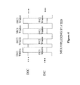
FIG. 4 is a block diagram of an exemplary synchronizing block shown in FIG. 3D.
FIG. 5 is a block diagram of an example of a circuit for generating the control signals of FIG. 3.
FIG. 6 is a timing diagram for illustrating the states of the multiplexers of FIG. 4.
FIG. 7 is a diagram representing discrete values of four output clock phases available from the phase rotator of FIG. 3D.
FIG. 8A is a graph showing test results from the phase rotator of FIG. 3D with no control inputs applied.
FIG. 8B is an exemplary layout of a phase rotator in accordance with one aspect of the invention.
FIG. 9 is a graph showing test results from the phase rotator of FIG. 3D with an increment pulses applied at 1/16th of the clock frequency.
FIG. 10 is a graph showing test results from the phase rotator of FIG. 3D with decrement pulses applied at 1/16th of the clock frequency.
FIG. 11A is a graph showing test results from the phase rotator of FIG. 3D with two decrement pulses applied at 1/16th of the clock frequency.
FIG. 11B is a graph showing test results from the phase rotator of FIG. 3D with two increment pulses applied at 1/16th of the clock frequency.
FIGS. 12A, 12B and 12C show illustrations of high-speed test results with a master clock frequency of fm=16.384 GHz.
FIG. 13 shows the use of the phase rotator as part of a direct digital synthesizer.
DETAILED DESCRIPTION OF THE INVENTION
As discussed in the background of the invention, FIG. 1 shows a block diagram of a generic phase rotator or phase generator that has a master clock input, one or more phase-shifted clock outputs, and a control input. The control input may in general be an analog signal but the focus of this invention is on a digital control input signal.
The digital programmable phase generator of Kirichenko is described in pending patent application Ser. No. 11/243,020. As shown in FIG. 2, the phase generator of Kirichenko was able to adjust phase only in a single direction and therefore lacked the flexibility of the present invention.
FIG. 3A is a block diagram of a phase rotator in accordance with one aspect of the invention with one control bit being a decrement input (DEC0) and one bit being an increment input (INC0). The circuit comprises an inverter, toggle flip-flop (TFF), confluence buffer (CB) and latches. A decrement input (DEC0) causes the inverter to delay one pulse interval, retarding the timing of the pulse stream by one master clock period. Similarly an increment (INC0) input bypasses the first TFF to advance the timing of the output pulse stream by one clock period. Thus depending on the control inputs, the phase of the output pulse stream can be shifted by one clock period in any direction. The master clock is applied to a first inverter which is also connected to the DEC0 line. When a DEC0 pulse is present, the output of the inverter is stopped for the interval of a pulse and the decremented clock is then passed to a second inverter connected to the INC0 line. With no INC0 or DEC0 pulses present, the master clock will pass through the inverters without change. When the INC0 pulse is present on the inverter connected to the INC0 line, the bypass line connected to the INC0 line and connecting to the a confluence buffer (CB) as shown will advance the timing of the output pulse stream by one master clock period. Thus, the DEC0 pulse will delay a pulse from the master clock train applied through the TFF to CB and the latch by one clock period and the INC0 pulse will advance the timing of the output pulse train by one clock period. The latch is a type D flip-flop which insures that the pulses generated are synchronized to the master clock. In the preferred embodiment shown in FIG. 3A, a similar clocked latch is included in the bypass line that leads from the INC0 line to the CB. where the clock input to this clocked latch may be provided by the output of the first inverter.
FIG. 3B is a block diagram of a phase rotator that cascades a plurality of single bit phase rotators, such as shown in FIG. 3A to form a multi-bit phase rotator. Two multi-bit binary-weighted words INC, and DEC, serve as digital input words specifying the amount of phase shift increment or decrement respectively. In presence of both (m-bit increment and m-bit decrement) inputs, the resultant shift in phase corresponds to the difference between the increment and decrement number. Thus, N=NINC−NDEC. The bits of each digital word in FIG. 3B are related to the other as bits of a binary word that represent a number, whereas, in FIG. 3A and FIG. 3C the bits represent equal-weighted contributions to increment or decrement. Thus, by sending an m-bit binary number N to the control input of the phase rotator, we achieve a phase shift the output signal by 2πN2−m in any direction. One advantage of this generalized m-bit input is that the phase rotator can be made arbitrarily precise, if m is large enough.
FIG. 3C is a block diagram of a one bit phase rotator of FIG. 3A followed by a frequency divider to generate multiple phases of the output. The number of TFFs in the frequency chain depends on the required output frequency. In the absence of increment or decrement input, the circuit decimates the master clock by a factor of 2m, where m is a number of TFFs.
FIG. 3D is a block diagram of a phase rotator with a synchronizer-multiplexer front end. Four control inputs, namely DEC1, DEC2, INC1 and INC2 serve to control the phase shift. These inputs are applied to the synchronizing block SYNC which also receives an input from the master clock. The SYNC block will be described more hereinafter in conjunction with FIG. 4. Two outputs, a DEC output and an INC output, serve to cause an incrementing of the clock or a decrementing of the clock as discussed more hereinafter. The master clock is applied to an inverter which is also connected to the DEC line. When a DEC pulse is present, the output of the inverter is stopped for a pulse interval (master clock period) and the decremented clock is then passed to an inverter connected to the INC line. With no INC or DEC pulses present, the master clock will pass through the inverters without change. When the INC pulse is present on the inverter connected to the INC line, the bypass line connected to the INC line and connecting to the confluence buffer (CB) as shown will advance a pulse into the output pulse train. Thus, the DEC pulse will effectively delay a pulse from the master clock train applied through the TFF to the latch and the INC pulse will advance a pulse in that pulse train. The latch is a type D flip-flop which insures that the pulses generated are synchronized to the master clock.
The circuit of FIG. 3D is designed for 4 parallel one bit inputs, two each for increment and decrement. The two INC inputs have equal weights, which differs from a 2-binary-bit INC input (as in FIG. 3B) where the most significant bit (MSB) would have twice the weight of the least significant bit (LSB).
Note that in the example in FIG. 3D, the master clock operates at 32 GigaSamples per seconds (GS/s). The 32 GS/s clock is applied to a first toggle flip-flop (TFF) which divides a clock rate down to 16 GS/s. The first TFF after the latch, divides the master clock down to 8 GS/s and the subsequent TFF divides it down to 4 GS/s. The 4 GS/s outputs are applied to respected toggle flip-flops which are fed by regular and inverted outputs from the 4 GS/s TFF, thus producing four output phases at 2 GS/s each with each of the phases from a particular output TFF being in quadrature relationship.
FIG. 4 is a block diagram of an exemplary synchronizing block SYNC shown in FIG. 3. A synchronizer block is optional, but does make the phase rotator work better by reducing phase jitter. A master clock input 400 (e.g. operating at 32 GS/s) feeds a chain of dividers 410 and 420, producing clock signals at 32 GS/sec, 16 GS/sec, 8 GS/sec and 4 GS/sec. The last stage of the divider chain 420 produces regular and inverted outputs CLKφ1 and CLKφ2 each operating at 2 GS/s. In the example shown, the clocks CLKφ1 and CLKφ2 are applied to RSFQ multiplexers 430 and 440. The inputs DEC1 and DEC2 are alternatively selected by the multiplexer and applied to the output line DEC. Similarly, input lines INC1 and INC2 are multiplexed and applied sequentially to the output line INC. The DEC and the INC lines each have an output rate, in this example, at 4 GS/s. A series of latches 450 i and 450 j receive the output of the multiplexer 430 and 440 respectively. These latches serve to synchronize the phase transitions of the multiplexer outputs to the 4 GS/sec, the 8 GS/sec, 16 GS/sec and 32 GS/sec clock signals produced by the chain of dividers.
The multiplexing circuits discussed in conjunction with FIG. 4 operate differently from the confluence buffers of other figures. A confluence buffer (CB) merges two input pulse streams into a single output pulse stream. A confluence buffer has no protection for the case where two pulses come in at the same time—one of the two will be lost. In contrast, a proper multiplexer (MUX) provides for interleaving two input pulse streams together, using a two phase clock and latches to make sure that no pulses get lost. This is more complicated than a CB, but it is still a standard RSFQ circuit that is not the subject of the present invention.
The particular type of driver utilized depends upon the type of control input signal. If the input were analog, the driver could constitute a ΔΣ modulator that applies increment and decrement pulses in response to changes in the input signal. If the control input were a digital input, the INC and DEC pulses could represent whether or not the state of the control input is above or below a threshold level for the digital control input word. The particular type of driver is not important. Rather, the type of driver will vary depending upon the particular application to which the phase rotator is put. The INC and DEC inputs can be simply digital signals generated by a digital signal processor. These INC and DEC inputs may be multi-bit, binary inputs, or else single-bit over-sampled inputs.
FIG. 6 is a timing diagram illustrating the windows during which multiplexers of FIG. 4 permit RSFQ pulses from the various input lines of FIG. 3D, for example, to pass to respective output lines DEC and INC. The top timing line shows that the outputs of multiplexer 430 and 440 of FIG. 4, alternately produces windows during which an output signal corresponding to DEC1 and DEC2 can be applied to the DEC output in a repeated fashion. Similarly, the lower timeline labeled INC shows the output from multiplexer 430 and 440 of FIG. 4, which open windows that permit an alternating sequence of INC1 and INC2 signals to pass to the INC line output.
FIG. 7 is a diagram representing discrete values of four output clock phases available from the phase rotator of FIG. 3D. For the specific example shown in FIG. 3D, FIG. 4 shows the relative phase angles of each of the 4 clock outputs. There are four 1-bit input lines, two for a phase delay (decrement) and two for a phase advance (increment). A digital input on either increment line will advance the phase by one fine unit (360°/16=22.5°); input on both INC lines will advance the phase by two units, and similarly in the reverse direction for the DEC lines. Taking all 4 outputs together, the entire phase range is covered, with a precision of 1/16th. This is not ultra-high precision, but the circuit is optimized for high speed. The phase may be modulated at a rate of 2 GHz, the same rate as the output clock. This is why this circuit is appropriate as a digital phase modulator for a fast DAC. Such a phase rotator with multiple clock phases may also have application in generating a specially shaped output pulse, for equalization of high-speed digital amplifiers.
Several examples of low-frequency test results for the circuit of FIG. 3D are shown in FIGS. 8-11.
FIG. 8A is a graph showing test results from the phase rotator in FIG. 3D with no control inputs applied. Each output clock line generates an output pulse every 16 periods of the master clock. (The output amplifier toggles between voltage levels when an output pulse is generated.) The four clock phases are delayed by 4 master clock periods from each other, as expected.
FIG. 8B shows the chip layout of the entire phase rotator circuit of FIG. 3D, including input and output drivers, which was fabricated as a superconducting integrated circuit on a single mm chip using fabrication technology of 3-1 μm Nb Josephson junctions with critical current density 1 kA/cm2. It was tested in liquid helium at a temperature of 4.2 K, at low speed and at high speed.
FIG. 9 shows the corresponding results with a control input on one of the increment (INC) inputs, at a rate of 1/16th of the master clock. As a result, the output clocks are advanced by 1 master clock period, in the appropriate locations.
FIG. 10 shows the corresponding results for a control input pulse sequence on one of the decrement (DEC) lines, with the output clocks retarded by 1 master clock.
FIGS. 11A and 11B show the corresponding results for inputs on either 2 DEC lines or 2 INC lines. Note that INC and DEC pulses applied simultaneously cancel each other out, producing no net phase shift.
The results of a high-speed test of a circuit of FIG. 3D are shown in FIGS. 12A, 12B, and 12C, with a master clock frequency of fm=16.384 GHz. The power spectrum of the output is shown, with and without input control signals. When there is no input, the output clock frequency is at fc=fy/16=1024 MHz. With an increment input at 1024 MHz, the output frequency is shifted up to 1088 MHz, a fractional increase of 1/16th. With a decrement input at 1024 MHz, the output frequency is shifted down to 960 MHz, a fractional decrease of 1/16th. This is consistent with expectations, and shows how the phase rotator may also be used as a digitally controlled frequency shifter.
In one application of the phase rotator, it is used as part of a direct digital synthesizer.
FIG. 13 shows the use of the phase rotator as part of a waveform generator. The generator comprises a phase rotator, which drives an SFQ output amplifier. This circuit will create an analog waveform from a time-varying signal in digital form. The phase rotator employs a high resolution Digital-To-Phase Converter, in order to finely locate every single edge of the output signal at the right instant in the time domain. The time resolution of the digital-to-phase converter directly determines the spectral purity of the produced output signal. In the semiconductor industry the phase rotator is routinely used in high speed signaling circuits to generate precisely aligned clocks. In the implementation shown, the transmitter synthesis technique is also embedded in the phase rotator. The outputs of the rotator are used to drive the SFQ Output Amplifier for waveform generation.
Depending on the control input, the rotator is capable to shift the phase of the output pulse stream by either one or two clock periods in any direction. The increment inputs cause a negative phase shift shrinking the time period (phase advance) whereas the decrement inputs cause a positive phase shift increasing the time period (phase delay). To ensure extremely high accuracy, the phase rotator includes a synchronizer that synchronizes the low frequency control inputs to a very high frequency clock. The synchronizer consists of a chain of toggle flip-flops (TFF) to subdivide the master clock into its binary sub harmonics. The control inputs are stored in a latch, clocked by the binary sub harmonic of the master clock whose frequency is equal to the maximum control input frequency. The two increment control inputs at maximum rate of 2 GS/s are multiplexed on a single line to give a maximum rate of 4 GS/s. Similarly the decrement control inputs are multiplexed on a single line. The control inputs are further successively re-latched and read by the higher sub harmonic clock until it is finally read by the master clock itself and passed on to the phase modulator. Depending on these control inputs, the modulator either advances or retards the timing of the output pulse stream by one or two clock periods. FIG. 3D shows the conceptual design of the phase modulator used in this application.
To produce a synthesized signal, the phase rotator digitally modulates a pulse train. The modulated pulse train can then be amplified and passed through a low pass filter to generate an analog signal.
The design of the SFQ Output Amplifier is disclosed in U.S. Pat. No. 5,936,458.
While various embodiments of the present invention have been illustrated herein in detail, it should be apparent that modifications and adaptations to those embodiments may occur to those skilled in the art without departing from the scope of the present invention as set forth in the following claims.

Claims (18)

What is claimed is:
1. A digital phase adjustment circuit, configured to generate a multi-GHz signal, comprising:
a clock input port configured to receive a clock input signal;
at least two distinct input ports, comprising:
an advance phase input port configured to receive an advance phase input signal;
a retard phase input port configured to receive a retard phase input signal;
a logical device comprising an integrated circuit having at least two Josephson junctions, having a decimator, configured to respond to the clock input signal, the advance phase input signal, and the retard phase input signal; and
an output port of the logical device, configured to generate the multi-GHz signal representing:
a pulse train corresponding to a clock input signal decimated by the decimator, if neither an advance phase input signal nor a retard phase input signal is active,
a pulse train corresponding to a clock input signal decimated by the decimator, with at least one additional pulse, if the advance phase input signal is active and the retard phase input signal is inactive, and
a pulse train corresponding to the clock input signal decimated by the decimator, delayed by at least one clock input pulse, if the retard phase input signal is active and the advance phase input signal is inactive,
thereby having a phase selectively advanced in response to the advance phase input signal, and selectively retarded in response to the retard phase input signal.
2. The digital phase adjustment circuit of claim 1, wherein the multi-GHz signal is a phase modulated communication signal modulated by the advance phase input signal and the retard phase input signal.
3. The digital phase adjustment circuit of claim 2, further comprising a synchronizer circuit, wherein the advance phase input signal and the retard phase input signal are synchronized to the clock input signal, to reduce phase error in the multi-GHz signal.
4. The digital phase adjustment circuit of claim 2, wherein the clock input signal has a frequency of greater than about 16 GHz.
5. The digital phase adjustment circuit of claim 1, wherein the logical device acts to shift a frequency of the multi-GHz output signal in dependence on a frequency of a digital signal presented to at least one of the advance phase input port and the retard phase input port.
6. The digital phase adjustment circuit of claim 1, wherein the multi-GHz signal comprises a digitally modulated pulse train.
7. The digital phase adjustment circuit of claim 6, further comprising a circuit configured to amplify and filter the digitally modulated pulse train to generate a digitally synthesized analog signal.
8. The digital phase adjustment circuit of claim 1, wherein the Josephson junctions comprise Niobium.
9. The digital phase adjustment circuit of claim 1, further comprising a circuit configured to generate a dynamically equalized output of an amplifier.
10. The digital phase adjustment circuit of claim 1, wherein at least one of the advance phase input port and the retard phase input port is configured to receive a signal comprising a plurality of input bits.
11. The digital phase adjustment circuit of claim 1, wherein at least one of the advance phase input port and the retard phase input port is configured to receive a signal comprising a plurality of concurrent equal-weighted bits.
12. The digital phase adjustment circuit of claim 1, wherein at least one of the advance phase input port and the retard phase input port is configured to receive a signal comprising a plurality of binary-weighted bits.
13. A method of producing digital phase rotation, comprising:
receiving a multi-GHz clock input having a clock period;
receiving a digital control signal comprising an advance phase input signal through an advance phase input signal port and a retard phase input signal through a retard phase input signal port, the advance phase input signal port being distinct from the retard phase input signal port;
decimating the multi-GHz clock input to produce a decimated clock signal;
modulating the decimated clock signal in dependence on the advance phase input signal and the retard phase input signal, wherein if the advance phase input signal is inactive and the retard phase input signal is inactive, the decimated clock signal is produced unmodulated, if the advance phase input signal is active and the retard phase input signal is inactive, at least one pulse is added to the decimated clock signal, and if the advance phase input signal is inactive and the retard phase input signal is active, the decimated clock signal is delayed by at least one clock period; and
outputting the modulated decimated clock signal,
wherein at least one of the decimating and the modulating are performed using Rapid Single Flux Quantum logic.
14. The method according to claim 13, wherein the advance phase input signal and the retard phase input signal each comprise a plurality of digital signal bits.
15. The method of claim 13, wherein the modulated decimated clock signal is further decimated to produce a plurality of signals having a reduced frequency with respect to the decimated clock signal, having respectively different relative phases.
16. The method of claim 13, wherein the digital control signal comprises a concurrent plurality of bits acting to define a modulation of the phase of the modulated decimated clock signal.
17. The method of claim 13, wherein at least one of the decimating and the modulating are performed using a plurality of flip-flops, clocked inverters, and clocked latches.
18. A method of producing digital phase rotation, comprising:
receiving a clock input at a frequency of at least about 16 GHz;
receiving a multibit parallel representation of a digital phase control signal;
subdividing the clock to generate a reduced-frequency decimated output of at least about 1 GHz; and
modulating a phase of the reduced frequency decimated output in multiples of the clock input, to advance and retard the phase of the reduced frequency output selectively in dependence on the multibit parallel representation of the digital control signal having at least four parallel input signals,
wherein in at least one first state of the multibit parallel representation of the digital control signal, at least one additional pulse of the clock input is added to the reduced frequency decimated output, in at least one second state of the multibit parallel representation of the digital control signal, the reduced frequency decimated output is delayed by a period of the clock input, and in at least one third state of the multibit parallel representation of the digital control signal, the reduced frequency decimated output is unchanged, such that the at least one first state produces an advanced phase of the reduced frequency decimated output, and the at least one second state produces a retarded phase of the reduced frequency decimated output,
wherein at least one of the subdividing and the modulating are performed using Rapid Single Flux Quantum logic.
US13/073,942 2005-10-04 2011-03-28 Superconducting digital phase rotator Active 2029-07-24 US9065452B1 (en)

Priority Applications (4)

Application Number Priority Date Filing Date Title
US13/073,942 US9065452B1 (en) 2006-12-29 2011-03-28 Superconducting digital phase rotator
US14/743,409 US9344069B1 (en) 2005-10-04 2015-06-18 Superconducting digital phase rotator
US15/155,687 US9748937B1 (en) 2006-08-25 2016-05-16 Superconducting digital phase rotator
US15/687,020 US10355681B1 (en) 2006-08-25 2017-08-25 Superconducting digital phase rotator

Applications Claiming Priority (3)

Application Number Priority Date Filing Date Title
US61780606A 2006-12-29 2006-12-29
US11/625,013 US7917798B2 (en) 2005-10-04 2007-01-19 Superconducting digital phase rotator
US13/073,942 US9065452B1 (en) 2006-12-29 2011-03-28 Superconducting digital phase rotator

Related Parent Applications (1)

Application Number Title Priority Date Filing Date
US11/625,013 Continuation US7917798B2 (en) 2005-10-04 2007-01-19 Superconducting digital phase rotator

Related Child Applications (1)

Application Number Title Priority Date Filing Date
US14/743,409 Continuation US9344069B1 (en) 2005-10-04 2015-06-18 Superconducting digital phase rotator

Publications (1)

Publication Number Publication Date
US9065452B1 true US9065452B1 (en) 2015-06-23

Family

ID=53397240

Family Applications (5)

Application Number Title Priority Date Filing Date
US11/625,013 Expired - Fee Related US7917798B2 (en) 2005-10-04 2007-01-19 Superconducting digital phase rotator
US13/073,942 Active 2029-07-24 US9065452B1 (en) 2005-10-04 2011-03-28 Superconducting digital phase rotator
US14/743,409 Active US9344069B1 (en) 2005-10-04 2015-06-18 Superconducting digital phase rotator
US15/155,687 Active US9748937B1 (en) 2006-08-25 2016-05-16 Superconducting digital phase rotator
US15/687,020 Expired - Fee Related US10355681B1 (en) 2006-08-25 2017-08-25 Superconducting digital phase rotator

Family Applications Before (1)

Application Number Title Priority Date Filing Date
US11/625,013 Expired - Fee Related US7917798B2 (en) 2005-10-04 2007-01-19 Superconducting digital phase rotator

Family Applications After (3)

Application Number Title Priority Date Filing Date
US14/743,409 Active US9344069B1 (en) 2005-10-04 2015-06-18 Superconducting digital phase rotator
US15/155,687 Active US9748937B1 (en) 2006-08-25 2016-05-16 Superconducting digital phase rotator
US15/687,020 Expired - Fee Related US10355681B1 (en) 2006-08-25 2017-08-25 Superconducting digital phase rotator

Country Status (1)

Country Link
US (5) US7917798B2 (en)

Cited By (2)

* Cited by examiner, † Cited by third party
Publication number Priority date Publication date Assignee Title
US9473124B1 (en) 2009-10-12 2016-10-18 Hypres, Inc. Low-power biasing networks for superconducting integrated circuits
US9748937B1 (en) 2006-08-25 2017-08-29 Hypres, Inc. Superconducting digital phase rotator

Families Citing this family (11)

* Cited by examiner, † Cited by third party
Publication number Priority date Publication date Assignee Title
US7991101B2 (en) * 2006-12-20 2011-08-02 Broadcom Corporation Multiple channel synchronized clock generation scheme
US8045660B1 (en) 2007-05-23 2011-10-25 Hypres, Inc. Wideband digital spectrometer
CA2962732C (en) * 2014-10-29 2020-02-18 Northrop Grumman Systems Corporation Reciprocal quantum logic (rql) circuit synthesis
KR102298160B1 (en) 2015-08-13 2021-09-03 삼성전자주식회사 Semiconductor device and the communication system including thereof
US10622032B2 (en) 2015-12-08 2020-04-14 Rambus Inc. Low power signaling interface
US10587245B1 (en) * 2018-11-13 2020-03-10 Northrop Grumman Systems Corporation Superconducting transmission line driver system
CN110311662A (en) * 2019-05-27 2019-10-08 中国科学院计算技术研究所 Superconducting ring and superconduction high-frequency clock generator
US11030369B2 (en) * 2019-09-04 2021-06-08 Microsoft Technology Licensing, Llc Superconducting circuit with virtual timing elements and related methods
US11545288B2 (en) 2020-04-15 2023-01-03 Northrop Grumman Systems Corporation Superconducting current control system
US20220344563A1 (en) * 2021-04-27 2022-10-27 Microsoft Technology Licensing, Llc Interfacing with superconducting circuitry
US11757467B2 (en) 2021-08-13 2023-09-12 Northrop Grumman Systems Corporation Circuits for converting SFQ-based RZ and NRZ signaling to bilevel voltage NRZ signaling

Citations (11)

* Cited by examiner, † Cited by third party
Publication number Priority date Publication date Assignee Title
US5355092A (en) * 1992-06-26 1994-10-11 Sanyo Electric Co., Ltd. Relatively simple QPSK demodulator, that uses substantially all digital circuitry and an internally generated symbol clock, and circuitry for use therein
US20020009170A1 (en) * 2000-05-26 2002-01-24 International Business Machines Corporation Phase rotator and data recovery receiver incorporating said phase rotator
US20020191256A1 (en) * 2001-05-31 2002-12-19 Schemmann Marcel F.C. Method and system for 80 and 160 gigabit-per-second QRZ transmission in 100 GHz optical bandwidth with enhanced receiver performance
US6756925B1 (en) * 2003-04-18 2004-06-29 Northrop Grumman Corporation PSK RSFQ output interface
US20040152965A1 (en) * 1997-04-14 2004-08-05 Diab Mohamed K. Method and apparatus for demodulating signals in a pulse oximetry system
US20050062526A1 (en) * 2003-06-02 2005-03-24 Morris Bradley John High-efficiency amplifier, converter and methods
US20060083293A1 (en) * 2004-10-18 2006-04-20 Keegan Richard G Phase multi-path mitigation
US20060208811A1 (en) * 2005-03-21 2006-09-21 An-Ming Lee Multi-phase clock generator and method thereof
US20070127600A1 (en) * 2005-12-06 2007-06-07 Fujitsu Limited Timing recovery circuit
US20070160168A1 (en) * 2006-01-11 2007-07-12 Beukema Troy J Apparatus and method for signal phase control in an integrated radio circuit
US7953174B2 (en) 2002-03-20 2011-05-31 The Regents Of The University Of California Radio transmission frequency digital signal generation

Family Cites Families (97)

* Cited by examiner, † Cited by third party
Publication number Priority date Publication date Assignee Title
FR2296322A1 (en) 1974-12-27 1976-07-23 Ibm France DIGITAL DATA DETECTION SYSTEM TRANSMITTED BY MODULATION OF A CARRIER
FR2335109A1 (en) * 1975-12-09 1977-07-08 Ibm France STATISTICAL DATA DETECTION METHOD AND DEVICE
GB2172719B (en) 1985-03-22 1988-10-05 Stc Plc Digital phase rotation of signals
US5134464A (en) 1990-11-16 1992-07-28 North American Philips Corporation Method and apparatus for the transmission and reception of a multicarrier digital television signal
US5282019A (en) 1988-10-03 1994-01-25 Carlo Basile Method and apparatus for the transmission and reception of a multicarrier digital television signal
US6693951B1 (en) 1990-06-25 2004-02-17 Qualcomm Incorporated System and method for generating signal waveforms in a CDMA cellular telephone system
US5103459B1 (en) 1990-06-25 1999-07-06 Qualcomm Inc System and method for generating signal waveforms in a cdma cellular telephone system
SE469616B (en) 1991-12-23 1993-08-02 Ellemtel Utvecklings Ab DEVICE FOR TRANSFER OF THE PHASE OF A CLOCK SIGNAL AND SET AND DEVICE FOR TASK RECOVERY OF A DIGITAL DATA SIGNAL
US5202693A (en) 1992-03-25 1993-04-13 Rockwell International Corporation GPS signal processing with 5-level carrier injection demodulation function using dual 3-level single sideband mixers
US5272479A (en) * 1992-07-22 1993-12-21 Trw Inc. High sensitivity superconductive digitizer
US5451894A (en) * 1993-02-24 1995-09-19 Advanced Micro Devices, Inc. Digital full range rotating phase shifter
MY112371A (en) 1993-07-20 2001-05-31 Qualcomm Inc System and method for orthogonal spread spectrum sequence generation in variable data rate systems
US5471497A (en) 1993-11-01 1995-11-28 Zehavi; Ephraim Method and apparatus for variable rate signal transmission in a spread spectrum communication system using coset coding
US5414728A (en) 1993-11-01 1995-05-09 Qualcomm Incorporated Method and apparatus for bifurcating signal transmission over in-phase and quadrature phase spread spectrum communication channels
US5793656A (en) 1994-06-30 1998-08-11 Hughes Electronics Corporation Application-specific integrated circuits having programming functions
AU3361095A (en) 1994-08-05 1996-03-04 Acuson Corporation Method and apparatus for transmit beamformer system
US5928152A (en) 1994-08-05 1999-07-27 Acuson Corporation Method and apparatus for a baseband processor of a receive beamformer system
US5581517A (en) 1994-08-05 1996-12-03 Acuson Corporation Method and apparatus for focus control of transmit and receive beamformer systems
US5675554A (en) 1994-08-05 1997-10-07 Acuson Corporation Method and apparatus for transmit beamformer
US5685308A (en) 1994-08-05 1997-11-11 Acuson Corporation Method and apparatus for receive beamformer system
US5555534A (en) 1994-08-05 1996-09-10 Acuson Corporation Method and apparatus for doppler receive beamformer system
US6029116A (en) 1994-08-05 2000-02-22 Acuson Corporation Method and apparatus for a baseband processor of a receive beamformer system
US5600675A (en) 1994-09-07 1997-02-04 General Electric Company Ultrasonic imager having improved bandwidth
US6185246B1 (en) 1994-09-21 2001-02-06 Qualcomm Incorporated System and method for orthogonal spread spectrum sequence generation in variable data rate systems
US5565866A (en) * 1994-10-04 1996-10-15 The United States Of America As Represented By The Secretary Of Commerce Digital-to-analog converter with voltage defined by Josephson frequency voltage relation
DE69534422T2 (en) * 1994-12-05 2006-07-06 Ntt Mobile Communications Network Inc. Signal multiplexer
US5602833A (en) 1994-12-19 1997-02-11 Qualcomm Incorporated Method and apparatus for using Walsh shift keying in a spread spectrum communication system
US5691974A (en) 1995-01-04 1997-11-25 Qualcomm Incorporated Method and apparatus for using full spectrum transmitted power in a spread spectrum communication system for tracking individual recipient phase, time and energy
US5577025A (en) 1995-06-30 1996-11-19 Qualcomm Incorporated Signal acquisition in a multi-user communication system using multiple walsh channels
US6393046B1 (en) 1996-04-25 2002-05-21 Sirf Technology, Inc. Spread spectrum receiver with multi-bit correlator
JPH09270827A (en) 1996-04-01 1997-10-14 Advantest Corp Parameter measurement instrument for digital orthogonal modulation signal
US6047017A (en) 1996-04-25 2000-04-04 Cahn; Charles R. Spread spectrum receiver with multi-path cancellation
US5798722A (en) * 1997-02-13 1998-08-25 Northrop Grumman Corporation UHF digital to analog converter for cryogenic radar system
TW465234B (en) * 1997-02-18 2001-11-21 Discovision Ass Single chip VLSI implementation of a digital receiver employing orthogonal frequency division multiplexing
US6249542B1 (en) 1997-03-28 2001-06-19 Sirf Technology, Inc. Multipath processing for GPS receivers
US5812078A (en) * 1997-05-22 1998-09-22 Northrop Grumman Corporation Josephson junction digital to analog converter for accurate AC waveform synthesis
US5936458A (en) 1997-07-21 1999-08-10 Hypres, Inc. Superconducting analog amplifier circuits
US6236344B1 (en) * 1998-07-02 2001-05-22 The United States Of America, As Represented By The Secretary Of Commerce AC and DC bipolar voltage source using quantized pulses
GB9818378D0 (en) 1998-08-21 1998-10-21 Nokia Mobile Phones Ltd Receiver
US6128678A (en) * 1998-08-28 2000-10-03 Theseus Logic, Inc. FIFO using asynchronous logic to interface between clocked logic circuits
US6310869B1 (en) 1998-08-31 2001-10-30 Qualcomm Incorporated Method and apparatus for reducing amplitude variations and interference in communication signals, such as in wireless communication signals employing inserted pilot symbols
US6466630B1 (en) 1999-01-27 2002-10-15 The Johns Hopkins University Symbol synchronization in a continuous phase modulation communications receiver
US6225936B1 (en) * 1999-06-04 2001-05-01 Trw Inc. Direct digital downconverter and method for converting an analog signal to a digital signal
US6463266B1 (en) 1999-08-10 2002-10-08 Broadcom Corporation Radio frequency control for communications systems
US6480529B1 (en) 1999-12-21 2002-11-12 Qualcomm, Incorporated Programmable matched filter searcher for multiple pilot searching
AU2820701A (en) 2000-01-18 2001-07-31 National Research Council Of Canada Parallel correlator archtitecture
US7376206B1 (en) 2000-11-06 2008-05-20 Qualcomm Incorporated Method and apparatus for adjusting the phase of a received signal
US6559800B2 (en) 2001-02-02 2003-05-06 Rosum Corporation Position location using broadcast analog television signals
US6518786B2 (en) * 2001-06-15 2003-02-11 Trw Inc. Combinational logic using asynchronous single-flux quantum gates
US7183971B1 (en) 2001-09-26 2007-02-27 Interstate Electronics Corporation Hybrid translator in a global positioning system (GPS)
JP3488224B2 (en) * 2001-11-16 2004-01-19 沖電気工業株式会社 Transition signal control device, DMA controller and transition signal control processor using the same
US6775530B2 (en) 2001-11-27 2004-08-10 Qualcomm Inc. Direct conversion of narrow-band RF signals
US7313199B2 (en) * 2002-03-21 2007-12-25 Hypres, Inc. Power amplifier linearization
US20040037311A1 (en) 2002-08-07 2004-02-26 Phonex Broadband Corporation Digital narrow band power line communication system
US7440490B2 (en) * 2002-12-18 2008-10-21 Anna Kidiyarova-Shevchenko Method and apparatus for multi-user detection using RSFQ successive interference cancellation in CDMA wireless systems
US6917216B2 (en) * 2003-04-11 2005-07-12 Northrop Grumman Corporation Superconductor output amplifier
US6750794B1 (en) * 2003-05-05 2004-06-15 Northrop Grumman Corporation Application of single flux quantum pulse interaction to the simultaneous sampling in-phase and quadrature analog-to-digital converter
US6917537B2 (en) * 2003-08-11 2005-07-12 Northrop Grumman Corporation RSFQ Batcher-banyan switching network
US7002499B2 (en) * 2004-01-21 2006-02-21 Hrl Laboratories, Llc Clocked D/A converter
US7486747B1 (en) 2004-07-09 2009-02-03 L-3 Communications Corporation Digital timing recovery operable at very low or less than zero dB Eb/No
US7522899B1 (en) 2004-07-15 2009-04-21 Marvell International Ltd. Image rejection scheme for receivers
US7505310B2 (en) * 2005-03-14 2009-03-17 Nec Corporation Method of configuring superconducting random access memory, device structure of the same, and superconducting drive circuit
US7593454B2 (en) 2005-07-28 2009-09-22 Itt Manufacturing Enterprises, Inc. Enhanced QPSK or DQPSK data demodulation for direct sequence spreading (DSS) system waveforms using orthogonal or near-orthogonal spreading sequences
US7609755B2 (en) 2005-07-28 2009-10-27 Itt Manufacturing Enterprises, Inc. Simplified timing correction for data despreading of serial offset quadrature pulse-shaped spread signals
US7529320B2 (en) 2005-09-16 2009-05-05 Agere Systems Inc. Format efficient timing acquisition for magnetic recording read channels
US7508230B2 (en) 2005-10-04 2009-03-24 Hypres, Inc. Digital programmable phase generator
US7917798B2 (en) 2005-10-04 2011-03-29 Hypres, Inc. Superconducting digital phase rotator
KR100724098B1 (en) * 2006-05-10 2007-06-04 한국표준과학연구원 A analogue-digital converter using josephson dac and method thereof
US8090043B2 (en) 2006-11-20 2012-01-03 Broadcom Corporation Apparatus and methods for compensating for signal imbalance in a receiver
US7724840B2 (en) 2006-12-19 2010-05-25 Crestcom, Inc. RF transmitter with predistortion and method therefor
US20080285640A1 (en) 2007-05-15 2008-11-20 Crestcom, Inc. RF Transmitter With Nonlinear Predistortion and Method Therefor
US8509208B2 (en) 2008-02-01 2013-08-13 Qualcomm Incorporated Frequency error estimation
US8885738B2 (en) 2008-03-26 2014-11-11 Csr Technology Inc. Unified single and multiple carrier receiver architecture
US8401108B1 (en) 2008-09-11 2013-03-19 L-3 Communications Corp Modulation and demodulation of band-limited signals using near-Nyquist sampling
EP2457328B1 (en) 2009-07-24 2014-03-26 Technion Research and Development Foundation, Ltd. Ultra-high-speed photonic-enabled adc based on multi-phase interferometry
US7978009B2 (en) 2009-08-03 2011-07-12 Telefonaktiebolaget Lm Ericsson (Publ) Digital modulated RF power amplifier with impedance compensation circuit
US8391426B2 (en) 2009-11-18 2013-03-05 California Institute Of Technology Broadband phase synthesis network with self-healing capability
US8724739B2 (en) 2010-11-09 2014-05-13 Raytheon Company Variable phase shifter-attenuator
US9503284B2 (en) 2011-06-10 2016-11-22 Technion Research And Development Foundation Ltd. Receiver, transmitter and a method for digital multiple sub-band processing
WO2013048525A1 (en) 2011-10-01 2013-04-04 Intel Corporation Digital fractional frequency divider
US8896474B2 (en) 2012-02-16 2014-11-25 Stichting Voor De Technische Wetenschappen Two-stage phase digitizer
US8461901B1 (en) 2012-02-17 2013-06-11 Raytheon Company Harmonic reject mixer with active phase mismatch compensation in the local oscillator path
US9557243B2 (en) 2012-03-14 2017-01-31 Axonoptics Llc Integrated optics reflectometer
US9222850B2 (en) 2013-03-14 2015-12-29 Axonoptics, Llc Integrated optics reflectometer
US8938043B2 (en) 2012-03-29 2015-01-20 Terasquare Co., Ltd. Adaptive optimum CDR bandwidth estimation by using a kalman gain extractor
US9201412B2 (en) 2012-05-01 2015-12-01 John G. Posa Wireless remote with control code learning
US8786337B2 (en) 2012-05-14 2014-07-22 Ensphere Solutions, Inc. Low jitter clock generator for multiple lanes high speed data transmitter
US8990864B2 (en) 2012-06-12 2015-03-24 Maxlinear, Inc. Method and system for receiver configuration based on a priori knowledge of noise
EP2887881A4 (en) 2012-08-24 2016-09-28 Volcano Corp System and method for focusing ultrasound image data
US9334069B1 (en) 2012-10-23 2016-05-10 The Boeing Company Propellant gauging at microgravity within the pressure—temperature—density inflection zone of xenon
US20140211779A1 (en) 2013-01-31 2014-07-31 University Of Southern California Scalable synchronization for distributed multiuser mimo
US9876501B2 (en) 2013-05-21 2018-01-23 Mediatek Inc. Switching power amplifier and method for controlling the switching power amplifier
US9048847B2 (en) 2013-09-24 2015-06-02 Analog Devices Global Apparatus and methods for synchronizing phase-locked loops
US9065653B2 (en) 2013-11-01 2015-06-23 Korea Advanced Institute Of Science & Technology Internal jitter tolerance tester with an internal jitter generator
US9407274B2 (en) 2014-04-29 2016-08-02 Telefonaktiebolaget L M Ericsson (Publ) Local oscillator interference cancellation
US9276792B1 (en) 2014-09-20 2016-03-01 Stiching Vour de Technische Wetenschappen Phase-domain digitizer
US9385651B2 (en) 2014-10-03 2016-07-05 Short Circuit Technologies Llc 60 GHz frequency generator incorporating third harmonic boost and extraction

Patent Citations (11)

* Cited by examiner, † Cited by third party
Publication number Priority date Publication date Assignee Title
US5355092A (en) * 1992-06-26 1994-10-11 Sanyo Electric Co., Ltd. Relatively simple QPSK demodulator, that uses substantially all digital circuitry and an internally generated symbol clock, and circuitry for use therein
US20040152965A1 (en) * 1997-04-14 2004-08-05 Diab Mohamed K. Method and apparatus for demodulating signals in a pulse oximetry system
US20020009170A1 (en) * 2000-05-26 2002-01-24 International Business Machines Corporation Phase rotator and data recovery receiver incorporating said phase rotator
US20020191256A1 (en) * 2001-05-31 2002-12-19 Schemmann Marcel F.C. Method and system for 80 and 160 gigabit-per-second QRZ transmission in 100 GHz optical bandwidth with enhanced receiver performance
US7953174B2 (en) 2002-03-20 2011-05-31 The Regents Of The University Of California Radio transmission frequency digital signal generation
US6756925B1 (en) * 2003-04-18 2004-06-29 Northrop Grumman Corporation PSK RSFQ output interface
US20050062526A1 (en) * 2003-06-02 2005-03-24 Morris Bradley John High-efficiency amplifier, converter and methods
US20060083293A1 (en) * 2004-10-18 2006-04-20 Keegan Richard G Phase multi-path mitigation
US20060208811A1 (en) * 2005-03-21 2006-09-21 An-Ming Lee Multi-phase clock generator and method thereof
US20070127600A1 (en) * 2005-12-06 2007-06-07 Fujitsu Limited Timing recovery circuit
US20070160168A1 (en) * 2006-01-11 2007-07-12 Beukema Troy J Apparatus and method for signal phase control in an integrated radio circuit

Cited By (3)

* Cited by examiner, † Cited by third party
Publication number Priority date Publication date Assignee Title
US9748937B1 (en) 2006-08-25 2017-08-29 Hypres, Inc. Superconducting digital phase rotator
US10355681B1 (en) 2006-08-25 2019-07-16 Hypres, Inc. Superconducting digital phase rotator
US9473124B1 (en) 2009-10-12 2016-10-18 Hypres, Inc. Low-power biasing networks for superconducting integrated circuits

Also Published As

Publication number Publication date
US20080049885A1 (en) 2008-02-28
US7917798B2 (en) 2011-03-29
US9344069B1 (en) 2016-05-17
US9748937B1 (en) 2017-08-29
US10355681B1 (en) 2019-07-16

Similar Documents

Publication Publication Date Title
US10355681B1 (en) Superconducting digital phase rotator
US8183902B2 (en) Methods and systems for digital pulse width modulator
US6781435B1 (en) Apparatus and method for converting a multi-bit signal to a serial pulse stream
US7365663B2 (en) Flux-quantizing superconducting analog to digital converter (ADC)
US7554369B2 (en) Digital programmable frequency divider
US6002279A (en) Clock recovery circuit
JP5749372B2 (en) Time / digital conversion using analog dithering
US8537953B2 (en) Time-interleaved clock-data recovery and method thereof
US10840917B1 (en) Clock alignment system having a dual-loop delay-locked loop
EP0813153A3 (en) Serial-to-parallel converter in a data communication system
Wu et al. A 1–16 Gb/s all-digital clock and data recovery with a wideband high-linearity phase interpolator
US20080310568A1 (en) Digital Sampling Apparatuses and Methods
CN107222210B (en) DDS system capable of configuring digital domain clock phase by SPI
US8031783B1 (en) Phase noise shaping using sigma delta modulation in a timing recovery unit
Turner et al. Phase coherent frequency hopping in direct digital synthesizers and phase locked loops
Cheng et al. A high resolution DPWM based on synchronous phase-shifted circuit and delay line
US6035409A (en) 1000 mb phase picker clock recovery architecture using interleaved phase detectors
US8164501B2 (en) Method and system for time interleaved digital to analog conversion for a cable modem
Lin et al. A 5-bit phase-interpolator-based fractional-N frequency divider for digital phase-locked loops
CN109889197B (en) Multi-path coherent frequency synthesis circuit based on linear frequency modulation continuous waveform
Kaplunenko et al. Superconducting single flux quantum 20 Gb/s clock recovery circuit
JPH0222926A (en) Semiconductor integrated circuit device
EP2355351A1 (en) Improved RTZ pulse generator
JPH0661993A (en) Clock extracting circuit and method therefor
JPS588179B2 (en) Digital jitter generator

Legal Events

Date Code Title Description
STCF Information on status: patent grant

Free format text: PATENTED CASE

MAFP Maintenance fee payment

Free format text: PAYMENT OF MAINTENANCE FEE, 4TH YR, SMALL ENTITY (ORIGINAL EVENT CODE: M2551); ENTITY STATUS OF PATENT OWNER: SMALL ENTITY

Year of fee payment: 4

AS Assignment

Owner name: AVIDBANK, CALIFORNIA

Free format text: SECURITY INTEREST;ASSIGNOR:HYPRES, INC.;REEL/FRAME:056617/0116

Effective date: 20200518

MAFP Maintenance fee payment

Free format text: PAYMENT OF MAINTENANCE FEE, 8TH YR, SMALL ENTITY (ORIGINAL EVENT CODE: M2552); ENTITY STATUS OF PATENT OWNER: SMALL ENTITY

Year of fee payment: 8