US9071126B2 - Wireless power transmission device - Google Patents

Wireless power transmission device Download PDF

Info

Publication number
US9071126B2
US9071126B2 US13/751,131 US201313751131A US9071126B2 US 9071126 B2 US9071126 B2 US 9071126B2 US 201313751131 A US201313751131 A US 201313751131A US 9071126 B2 US9071126 B2 US 9071126B2
Authority
US
United States
Prior art keywords
phase
power
signal
voltage
feedback
Prior art date
Legal status (The legal status is an assumption and is not a legal conclusion. Google has not performed a legal analysis and makes no representation as to the accuracy of the status listed.)
Active, expires
Application number
US13/751,131
Other versions
US20140092659A1 (en
Inventor
Huang-Ti Lin
Yueh-Han Li
Tsung-Shiun Lee
Jia-Wei Liu
Current Assignee (The listed assignees may be inaccurate. Google has not performed a legal analysis and makes no representation or warranty as to the accuracy of the list.)
AU Optronics Corp
Original Assignee
AU Optronics Corp
Priority date (The priority date is an assumption and is not a legal conclusion. Google has not performed a legal analysis and makes no representation as to the accuracy of the date listed.)
Filing date
Publication date
Application filed by AU Optronics Corp filed Critical AU Optronics Corp
Assigned to AU OPTRONICS CORP. reassignment AU OPTRONICS CORP. ASSIGNMENT OF ASSIGNORS INTEREST (SEE DOCUMENT FOR DETAILS). Assignors: LEE, TSUNG-SHIUN, LI, YUEH-HAN, LIN, HUANG-TI, LIU, Jia-wei
Publication of US20140092659A1 publication Critical patent/US20140092659A1/en
Priority to US14/712,897 priority Critical patent/US20150270721A1/en
Application granted granted Critical
Publication of US9071126B2 publication Critical patent/US9071126B2/en
Active legal-status Critical Current
Adjusted expiration legal-status Critical

Links

Images

Classifications

    • HELECTRICITY
    • H02GENERATION; CONVERSION OR DISTRIBUTION OF ELECTRIC POWER
    • H02JCIRCUIT ARRANGEMENTS OR SYSTEMS FOR SUPPLYING OR DISTRIBUTING ELECTRIC POWER; SYSTEMS FOR STORING ELECTRIC ENERGY
    • H02J50/00Circuit arrangements or systems for wireless supply or distribution of electric power
    • H02J50/10Circuit arrangements or systems for wireless supply or distribution of electric power using inductive coupling
    • HELECTRICITY
    • H02GENERATION; CONVERSION OR DISTRIBUTION OF ELECTRIC POWER
    • H02MAPPARATUS FOR CONVERSION BETWEEN AC AND AC, BETWEEN AC AND DC, OR BETWEEN DC AND DC, AND FOR USE WITH MAINS OR SIMILAR POWER SUPPLY SYSTEMS; CONVERSION OF DC OR AC INPUT POWER INTO SURGE OUTPUT POWER; CONTROL OR REGULATION THEREOF
    • H02M7/00Conversion of ac power input into dc power output; Conversion of dc power input into ac power output
    • H02M7/02Conversion of ac power input into dc power output without possibility of reversal
    • H02M7/04Conversion of ac power input into dc power output without possibility of reversal by static converters
    • H02M7/06Conversion of ac power input into dc power output without possibility of reversal by static converters using discharge tubes without control electrode or semiconductor devices without control electrode
    • H02J5/005

Definitions

  • Taiwan Patent Application No. 101135998 filed Sep. 28, 2012 and now Taiwan Patent No. 1473382, both included herein by reference in their entireties.
  • the present invention is related to a wireless power transmission device, and more particularly, to a wireless power transmission device having feedback control.
  • Wireless charging technology which utilizes non-contact wireless power transmission has been widely applied to mobile devices such as consumer electronics, smart phones, and tablet computers.
  • FIG. 1 is a diagram illustrating a prior art wireless charging module 100 .
  • the wireless charging module 100 includes a power transmitter 102 , a power receiver 104 , and a transmission unit 106 .
  • the transmission unit 106 utilizes inductive coils 108 and 110 as an antenna for transmitting and receiving power.
  • a radio frequency identification (RFID) system is included in the design of the wireless charging module 100 in order that an RFID feedback signal from the power receiver 104 can be transmitted to the power transmitter 102 by utilizing the same inductive coils 108 and 110 for controlling power transfer between the power transmitter 102 and the power receiver 104 .
  • RFID radio frequency identification
  • the RFID feedback signal's operating frequency is about several megahertz (MHz) and the RFID feedback signal is transmitted via the same inductive coils used to transmit power, the same inductive coils are required to transfer power and the RFID feedback signal.
  • the RFID feedback signal waveforms may be distorted by voltages induced by the power transmission on the inductive coils, thereby interfering the RFID feedback signal and causing control errors and instability of the wireless charging module 100 .
  • An embodiment of the present invention discloses a wireless power transmission device.
  • the wireless power transmission device comprises a power transmitter, a first transmission unit, a power receiver, a feedback regulator, a receive controller, and a second transmission unit.
  • the power transmitter generates power.
  • the first transmission unit is coupled to the power transmitter for wirelessly transmitting the power generated by the power transmitter.
  • the power receiver is coupled to the first transmission unit for receiving and rectifying the power from the first transmission unit.
  • the feedback regulator comprises a feedback receiver and a command adjuster.
  • the feedback receiver is coupled to the power receiver for receiving a feedback signal from the power receiver.
  • the command adjuster is coupled to the feedback receiver for generating an AC control signal.
  • the receive controller comprises a feedback judge controller and a control adjuster.
  • the feedback judge controller receives the control signal.
  • the control adjuster is coupled between the feedback judge controller and the power transmitter for generating a driving signal.
  • the second transmission unit is coupled between the feedback regulator and the receive controller for wirelessly transmitting the control signal to
  • the wireless power transmission device comprises a power transmitter, a first transmission unit, a power receiver, a feedback circuit, a phase feedback circuit, a controller, and a regulator device.
  • the power transmitter generates power.
  • the first transmission unit is coupled to the power transmitter for wirelessly transmitting the power generated by the power transmitter.
  • the power receiver is coupled to the first transmission unit for receiving and rectifying the power from the first transmission unit.
  • the feedback circuit is coupled to the power receiver for detecting a rectified output voltage of the power receiver to generate a feedback control signal.
  • the phase feedback circuit is coupled to the power receiver for detecting a phase of an input voltage of the power receiver to generate a phase signal.
  • the controller is coupled between the feedback circuit and the phase feedback circuit for generating a compensating voltage according to the feedback control signal and the phase signal.
  • the regulator device is coupled between the controller and the power receiver for generating a regulating voltage according to the compensating voltage to regulate a pre-rectified output voltage of the power receiver by an in phase form or an out of phase form.
  • FIG. 1 is a diagram illustrating a prior art wireless charging module.
  • FIG. 2 is a diagram illustrating a wireless power transmission device according to an embodiment of the present invention.
  • FIG. 3A is a diagram illustrating the power transmitter according to an embodiment.
  • FIG. 3B is a diagram illustrating the power transmitter according to another embodiment.
  • FIG. 4A is a diagram illustrating the first compensating circuit according to an embodiment.
  • FIG. 4B is a diagram illustrating the first compensating circuit according to another embodiment.
  • FIG. 5A is a diagram illustrating the power receiver according to an embodiment.
  • FIG. 5B is a diagram illustrating the power receiver according to another embodiment.
  • FIG. 6A is a diagram illustrating the feedback regulator according to an embodiment.
  • FIG. 6B is a diagram illustrating the feedback regulator according to another embodiment.
  • FIG. 6C is a diagram illustrating the feedback regulator according to another embodiment.
  • FIG. 7 is a diagram illustrating the receive controller according to an embodiment.
  • FIG. 8 is a diagram illustrating a wireless power transmission device.
  • FIG. 9 is a diagram illustrating the feedback circuit according to an embodiment.
  • FIG. 10A is a diagram illustrating the phase feedback circuit according to an embodiment.
  • FIG. 10B is a diagram illustrating the phase feedback circuit according to another embodiment.
  • FIG. 10C is a diagram illustrating the phase feedback circuit according to another embodiment.
  • FIG. 10D is a diagram illustrating the phase feedback circuit according to another embodiment.
  • FIG. 10E is a diagram illustrating operations of the phase regulator.
  • FIG. 11 is a diagram illustrating the controller according to an embodiment.
  • FIG. 12A is a diagram illustrating the regulator device according to an embodiment.
  • FIG. 12B is a diagram illustrating the regulator device according to another embodiment.
  • FIG. 12C is a diagram illustrating operations of the regulator device.
  • FIG. 12D is another diagram illustrating operations of the regulator device.
  • the wireless power transmission device 200 may include a power transmitter 202 , a first transmission unit 206 , a power receiver 204 , a feedback regulator 212 , a receive controller 214 , and a second transmission unit 216 .
  • the first transmission unit 206 may include a first inductive element 2062 and a second inductive element 2064 .
  • the feedback regulator 212 may include a feedback receiver 2122 and a command adjuster 2124 .
  • the receive controller 214 may include a feedback judge controller 2142 and a control adjuster 2144 .
  • the second transmission unit may include a first conductive element 2162 and a second conductive element 2164 .
  • the power transmitter 202 is used to convert DC voltage to AC voltage having a predetermined frequency and amplitude.
  • FIG. 3A is a diagram illustrating the power transmitter 202 according to an embodiment.
  • FIG. 3A shows a full bridge converter 302 and a first compensating circuit 304 .
  • FIG. 3B is a diagram illustrating the power transmitter 202 according to another embodiment.
  • FIG. 3B shows a half bridge converter 312 and the first compensating circuit 304 .
  • PMOSs 306 and NMOSs 308 may be MOSFET, BJT, or IGBT transistors.
  • V outa is AC voltage outputting from the power transmitter 202 to the first inductive element 2062 .
  • FIG. 4A is a diagram illustrating the first compensating circuit 304 according to an embodiment.
  • the first compensating circuit 304 in FIG. 4A includes a capacitor and an inductor connected in parallel with the converter.
  • FIG. 4B is a diagram illustrating the first compensating circuit 304 according to another embodiment.
  • the first compensating circuit 304 in FIG. 4B includes a capacitor and an inductor connected in series with the converter. The inductor may be removed from the first compensating circuit 304 , leaving only the capacitor connected in parallel or in series with the converter to form the first compensating circuit 304 .
  • the first transmission unit 206 wirelessly transmits power generated by the power transmitter 202 .
  • the first inductive element 2062 is coupled to the power transmitter 202 .
  • the second inductive element 2064 is coupled to the power receiver 204 .
  • the first inductive element 2062 and the second inductive element 2064 may be inductive coils wound by multi-stranded wires and may induce the power to the power receiver 204 via magnetic coupling by continuously alternating magnetic field directions.
  • Each inductive element may be formed respectively by connecting a plurality of inductive coils in series or in parallel.
  • the power receiver 204 is used to convert AC voltage to DC voltage.
  • the power receiver 204 is coupled to the first transmission unit 206 for receiving and rectifying the power from the first transmission unit 206 .
  • FIG. 5A is a diagram illustrating the power receiver 204 according to an embodiment.
  • FIG. 5A shows a full bridge rectifier 502 and a second compensating circuit 504 .
  • FIG. 5B is a diagram illustrating the power receiver 204 according to another embodiment.
  • FIG. 5B shows a half bridge rectifier 512 and the second compensating circuit 504 .
  • Rectifiers in the power receiver 204 may be composed of other active components such as MOSFET or IGBT rectifiers.
  • V in is AC voltage inputting from the second inductive element 2064 to the power receiver 204
  • V dca is DC voltage outputting from the power receiver 204
  • the second compensating circuit 504 may be composed of a capacitor and an inductor connected in parallel or in series with the converter. The inductor may be removed from the second compensating circuit 504 , leaving only the capacitor connected in parallel or in series with the converter to form the second compensating circuit 504 .
  • the feedback receiver 2122 of the feedback regulator 212 is coupled to the power receiver 204 for receiving a feedback signal S fb from the power receiver 204 .
  • the feedback signal S fb may be a signal at any circuit node of the power receiver 204 , so the feedback signal S fb may be a DC signal or an AC signal and may be a voltage type or a current type.
  • the command adjuster 2124 of the feedback regulator 212 is coupled to the feedback receiver 2122 for generating an AC control signal S c .
  • FIG. 6A is a diagram illustrating the feedback regulator 212 according to an embodiment.
  • the feedback receiver 2122 of FIG. 6A may include a rectifier coupled to the power receiver 204 for receiving and rectifying the feedback signal S fb to be a first DC signal V dc1 .
  • the rectifier may include a first diode D 1 , a second diode D 2 , and a first capacitor C 1 .
  • the first diode D 1 has a first end coupled to the power receiver 204 for receiving the feedback signal S fb , and a second end for receiving a reference voltage GND.
  • the second diode D 2 has a first end and a second end, the second end being coupled to the first end of the first diode D 1 .
  • the first capacitor C 1 has a first end coupled to the first end of the second diode D 2 , and a second end for receiving the reference voltage GND.
  • the command adjuster 2124 of FIG. 6A may include a digital frequency modulator FM 1 and a resonant tank.
  • the digital frequency modulator FM 1 is coupled between the feedback receiver 2122 and the first conductive element 2162 for generating a first frequency signal V fre1 according to the first DC signal V dc1 .
  • the digital frequency modulator FM 1 modulates the first frequency signal V fre1 corresponding to a varying voltage level of the first DC signal V dc1 .
  • the resonant tank is composed of a second capacitor C 2 and a first inductor L 1 and is coupled to the digital frequency modulator FM 1 for generating the control signal S c according to the first frequency signal V fre1 .
  • FIG. 6B is a diagram illustrating the feedback regulator 212 according to another embodiment.
  • the feedback receiver 2122 of FIG. 6B may include the same components as shown in FIG. 6A and is coupled to the power receiver 204 for receiving and rectifying the feedback signal S fb to be the first DC signal V dc1 .
  • the command adjuster 2124 of FIG. 6B may include the digital frequency modulator FM 1 and a first amplify circuit.
  • the digital frequency modulator FM 1 of FIG. 6B is coupled in the same way as in FIG. 6A and detailed description will be omitted.
  • the first amplify circuit may include a first amplifier OP 1 , a first resistor R 1 , and a second resistor R 2 .
  • the first amplify circuit is coupled to the digital frequency modulator FM 1 for generating the control signal S c by amplifying the first frequency signal V fre1 .
  • FIG. 6C is a diagram illustrating the feedback regulator 212 according to another embodiment.
  • the feedback receiver 2122 of FIG. 6C may include the rectifier, a duty modulator DM 1 , a second inductor L 2 , and a switch Q 1 .
  • the rectifier may include the same components as shown in FIG. 6A and is coupled to the power receiver 204 for receiving and rectifying the feedback signal S fb to be a second DC signal V dc2 .
  • a circuit formed by the duty modulator DM 1 , the second inductor L 2 , and the switch Q 1 may be used to receive the second DC signal V dc2 for generating a duty signal V fre2 corresponding to the second DC signal V dc2 .
  • the duty modulator DM 1 generates a duty cycle corresponding to a varying voltage level of the second DC signal V dc2 and the duty signal V fre2 is then generated by the circuit formed by the second inductor L 2 and the switch Q 1 so that duty cycle of the duty signal V fre2 varies corresponding to the voltage level of the second DC signal V dc2 .
  • the command adjuster 2124 of FIG. 6C may include a second amplify circuit.
  • the second amplify circuit may include a second amplifier OP 2 , a third resistor R 3 , and a fourth resistor R 4 .
  • the second amplify circuit is coupled to the feedback receiver 2122 for generating the control signal S c by amplifying the duty signal V fre2 .
  • the feedback judge controller 2142 of the receive controller 214 is for receiving the control signal S c .
  • the control adjuster 2144 of the receive controller 214 is coupled between the feedback judge controller 2142 and the power transmitter 202 for generating a driving signal S drv to adjust the power generated by the power transmitter 202 .
  • FIG. 7 is a diagram illustrating the receive controller 214 according to an embodiment.
  • the feedback judge controller 2142 in FIG. 7 may include a comparator CMP 1 and a rectifier.
  • the comparator CMP 1 is coupled between the second conductive element 2164 of the second transmission unit 216 and the control adjuster 2144 for receiving the AC control signal S c from the second transmission unit 216 and generating a phase signal V phase according to a voltage phase of the control signal S c .
  • the rectifier may include the same components as shown in FIG. 6A .
  • the rectifier is coupled between the second conductive element 2164 of the second transmission unit 216 and the control adjuster 2144 for generating an amplitude signal V amp according to a voltage amplitude of the control signal S c .
  • the control adjuster 2144 of FIG. 7 may be an analog circuit or a digital integrated circuit for interpreting a command implied in the voltage amplitude and frequency of the control signal S c so as to generate a driving signal S drv according to the phase signal V phase and the amplitude signal V amp .
  • the driving signal S drv contains plural sets of signals having continuously changing duty cycle and frequency for driving the converter of the power transmitter 202 to convert DC voltage to AC voltage.
  • the first conductive element 2162 of the second transmission unit 216 is coupled to the feedback regulator 212 .
  • the second conductive element 2164 is coupled to the receive controller 214 .
  • the first conductive element 2162 and the second conductive element 2164 are used to wirelessly transmit the control signal S c , and the first conductive element 2162 and the second conductive element 2164 do not contact physically.
  • a distance d between the first conductive element 2162 and the second conductive element 2164 may be an arbitrary value. Transmission of the control signal S c must be accurate and not be interfered, and power loss in the transmission should be as low as possible.
  • the first conductive element 2162 and the second conductive element 2164 may be conductive boards such as printed circuit boards, or metal probes in order to reduce interference and power loss.
  • the first conductive element 2162 and the second conductive element 2164 are respectively disposed in different housings, which are separated physically.
  • the control signal S c can be transmitted from the power receiver 204 to the power transmitter 202 without using RFID system and can be transmitted in a separate transmission unit other than the first transmission unit 206 used to the power transmission. In so doing, interference caused by coils may be reduced and control errors and instability may be alleviated, thereby increasing stability and power level that can be transferred.
  • FIG. 8 is a diagram illustrating a wireless power transmission device 800 .
  • the wireless power transmission device 800 may include a power transmitter 802 , a first transmission unit 806 , a power receiver 804 , a feedback circuit 812 , a phase feedback circuit 814 , a controller 816 , and a regulator device 810 .
  • the first transmission unit 806 may include a first inductive element 8062 and a second inductive element 8064 .
  • the feedback circuit 812 , the phase feedback circuit 814 , and the controller 816 may be an analog circuit, or be integrated in an analog integrated circuit or a digital integrated circuit.
  • Circuit structures of the power transmitter 802 and the first transmission unit 806 are the same as the power transmitter 202 and the first transmission unit 206 , detailed description being omitted.
  • the power receiver 804 is coupled to the first transmission unit 806 for receiving and rectifying the power from the first transmission unit 806 .
  • V in is an input voltage of the power receiver 804
  • V out is a pre-rectified output voltage of the power receiver 804
  • V dc is a rectified output voltage of the power receiver 804 .
  • the feedback circuit 812 is coupled to the power receiver 804 for detecting the rectified output voltage V dc of the power receiver 804 to generate a feedback control signal V fb .
  • the feedback control signal V fb may be a DC voltage signal.
  • FIG. 9 is a diagram illustrating the feedback circuit 812 according to an embodiment.
  • the feedback circuit 812 may include a third amplify circuit.
  • the third amplify circuit includes a third amplifier OP 3 , a first resistor R 1 , a second resistor R 2 , and a plurality of resistors R.
  • the first resistor R 1 and the second resistor R 2 of the feedback circuit 812 is used to divide the rectified output voltage V dc .
  • the third amplifier OP 3 compares the divided V dc with a predetermined voltage level V com and outputs a difference signal at an output end of the third amplifier OP 3 to be the feedback control signal V fb for the controller 816 .
  • the difference signal may be a positive voltage signal or a negative voltage signal so that the controller 816 may output a compensating voltage V d either in phase or out of phase to the regulator device 810 in order to control the rectified output voltage V dc of the power receiver 804 .
  • Amplitude of the feedback control signal V fb may be adjusted by adjusting values of the plurality of resistors R.
  • the feedback circuit 812 may be a subtractor.
  • the phase feedback circuit 814 is coupled to the power receiver 804 for detecting a phase of the input voltage V in of the power receiver 804 to generate a phase signal V p .
  • the phase signal V p may be an AC voltage signal.
  • FIG. 10A is a diagram illustrating the phase feedback circuit 814 according to an embodiment.
  • the phase feedback circuit 814 of FIG. 10A may include a fourth amplify circuit.
  • the fourth amplify circuit may include a fourth amplifier OP 4 and a plurality of resistors R, which form a non-inverting amplifier.
  • the phase signal V p may be adjusted to be bigger than the input voltage V in by adjusting values of the plurality of resistors R.
  • FIG. 10B is a diagram illustrating the phase feedback circuit 814 according to another embodiment.
  • the phase feedback circuit 814 of FIG. 10B may include a fifth and a sixth amplify circuits, which form two sets of inverting amplifiers.
  • the fifth amplify circuit may include a fifth amplifier OP 5 and a plurality of resistors R
  • the sixth amplify circuit may include a sixth amplifier OP 6 and a plurality of resistors R.
  • the phase signal V p may be adjusted to be smaller than the input voltage V in by adjusting values of the plurality of resistors R.
  • the purpose of adjusting the phase signal V p is that the controller 816 and the regulator device 810 can operate in a wider voltage range.
  • FIG. 10C is a diagram illustrating the phase feedback circuit 814 according to another embodiment.
  • the phase feedback circuit 814 of FIG. 10C may include the fourth amplify circuit of FIG. 10A and a phase regulator PR 1 .
  • the phase regulator PR 1 includes a zero cross detector and a bandpass filter (BPF). A zero cross of the input voltage V in is detected by the zero cross detector, then a phase of the zero cross is adjusted by the bandpass filter so that a phase adjusting signal V phe outputted by the phase regulator PR 1 has a phase different from the zero cross of the input voltage V in .
  • BPF bandpass filter
  • FIG. 10D is a diagram illustrating the phase feedback circuit 814 according to another embodiment.
  • the phase feedback circuit 814 of FIG. 10D may include the fifth and the sixth amplify circuits of FIG. 10B and the phase regulator PR 1 .
  • the phase regulator PR 1 is coupled to the fifth amplify circuit and has the same structure and purpose as set forth in FIG. 10C .
  • FIG. 10E is a diagram illustrating operations of the phase regulator PR 1 .
  • a square wave signal V z is generated when the input voltage V in passes through the zero cross detector, then a phase and an amplitude of the square wave signal V z is adjusted by the bandpass filter to generate the phase adjusting signal V phe outputted to the amplify circuits.
  • the phase adjusting signal V phe and the phase signal V p have phases different from the input voltage V in so that the controller 816 may output the compensating voltage V d having a phase difference to the regulator device 810 .
  • the controller 816 is coupled between the feedback circuit 812 and the phase feedback circuit 814 for generating the compensating voltage V d according to the feedback control signal V fb and the phase signal V p .
  • the feedback control signal V fb may be a DC voltage signal and the phase signal V p may be an AC voltage signal.
  • FIG. 11 is a diagram illustrating the controller 816 according to an embodiment.
  • the controller 816 may include a multiplier M 1 , a seventh amplifier OP 7 , an eighth amplifier OPA, and a plurality of resistors R.
  • the multiplier M 1 of the controller 816 multiplies the feedback control signal V fb and the phase signal V p to derive a predetermined compensating voltage.
  • a non-inverting amplifier composed of the seventh amplifier OP 7 , the eighth amplifier OPA, which is a high power amplifier, and a plurality of resistors R amplifies the predetermined compensating voltage to be the compensating voltage V d .
  • the seventh amplifier OP 7 is a voltage follower for stabilizing the predetermined compensating voltage
  • the eighth amplifier OPA is a high power amplifier for outputting the compensating voltage V d to the regulator device 810 so as to stabilize the pre-rectified output voltage V out .
  • the regulator device 810 is coupled between the controller 816 and the power receiver 804 for generating a regulating voltage V reg , which is in phase or out of phase with the input voltage V in , according to the compensating voltage V d to regulate the pre-rectified output voltage V out of the power receiver 804 .
  • FIG. 12A is a diagram illustrating the regulator device 810 according to an embodiment.
  • the regulator device 810 of FIG. 12A is a transformer having a primary winding PRI and a secondary winding SEC.
  • the primary winding PRI receives the compensating voltage V d from the controller 816 and the secondary winding SEC is connected in series between the input voltage V in and the pre-rectified output voltage V out .
  • FIG. 12B is a diagram illustrating the regulator device 810 according to another embodiment.
  • the regulator device 810 of FIG. 12B is a capacitor directly connected in series between the input voltage V in and the pre-rectified output voltage V out .
  • the compensating voltage V d in the case of FIG. 12B is substantially equal to the regulating voltage V reg .
  • the regulator device 810 may be composed of other passive components or coupling components other than those in FIG. 12A and FIG. 12B .
  • FIG. 12C is a diagram illustrating operations of the regulator device 810 .
  • the input voltage V in is lower than voltage required by the pre-rectified output voltage V out , so the regulator device 810 connected in series may add the regulating voltage V reg in phase with the input voltage V in to stabilize the pre-rectified output voltage V out .
  • FIG. 12D is another diagram illustrating operations of the regulator device 810 .
  • the input voltage V in is higher than voltage required by the pre-rectified output voltage V out , so the regulator device 810 connected in series may add the regulating voltage V reg out of phase with the input voltage V in to stabilize the pre-rectified output voltage V out .
  • the phase feedback circuit 814 may generate the phase signal V p having a phase different from the input voltage V in after detecting the phase of the input voltage V in , and the phase signal V p may be used to generate the regulating voltage V reg having a phase different from the input voltage V in through the controller 816 and the regulator device 810 to regulate the pre-rectified output voltage V out in order to compensate a power factor of the wireless power transmission device 800 .
  • embodiments of the present invention can transmit the control signal S c from the power transmitter 204 to the power receiver 202 without employing additional RFID chips and do not share the same first transmission unit 206 used for the power transmission.
  • the present invention can reduce interference, control errors, and instability, thereby increasing stability and power level of wireless power transmission.
  • Embodiments of the present invention also provide simple circuit structures as the regulator device 810 to regulate the pre-rectified output voltage V out by using a voltage in phase or out of phase with the input voltage V in so as to stabilize the pre-rectified output voltage V out and the rectified output voltage V dc /thus no additional DC to DC converter is required to be employed in the power receiver 804 .

Abstract

A wireless power transmission device includes a power transmitter, a first transmission unit, a power receiver, a feedback regulator, a receive controller, and a second transmission unit. The power transmitter is for generating power, and the first transmission unit is for wirelessly transmitting power generated by the power transmitter. The power receiver is for receiving and rectifying the power from the first transmission unit. The feedback regulator is for receiving a feedback signal from the power receiver to generate an AC control signal. The receive controller is for receiving the control signal to generate a driving signal. The second transmission unit is for wirelessly transmitting the control signal to the receive controller.

Description

CROSS-REFERENCE TO RELATED APPLICATIONS
This application claims the benefit of priority to Taiwan Patent Application No. 101135998, filed Sep. 28, 2012 and now Taiwan Patent No. 1473382, both included herein by reference in their entireties.
BACKGROUND OF THE INVENTION
1. Field of the Invention
The present invention is related to a wireless power transmission device, and more particularly, to a wireless power transmission device having feedback control.
2. Related Art
Wireless charging technology which utilizes non-contact wireless power transmission has been widely applied to mobile devices such as consumer electronics, smart phones, and tablet computers.
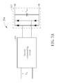
Please refer to FIG. 1. FIG. 1 is a diagram illustrating a prior art wireless charging module 100. The wireless charging module 100 includes a power transmitter 102, a power receiver 104, and a transmission unit 106. The transmission unit 106 utilizes inductive coils 108 and 110 as an antenna for transmitting and receiving power. A radio frequency identification (RFID) system is included in the design of the wireless charging module 100 in order that an RFID feedback signal from the power receiver 104 can be transmitted to the power transmitter 102 by utilizing the same inductive coils 108 and 110 for controlling power transfer between the power transmitter 102 and the power receiver 104.
Due to the fact that the RFID feedback signal's operating frequency is about several megahertz (MHz) and the RFID feedback signal is transmitted via the same inductive coils used to transmit power, the same inductive coils are required to transfer power and the RFID feedback signal. Thus the RFID feedback signal waveforms may be distorted by voltages induced by the power transmission on the inductive coils, thereby interfering the RFID feedback signal and causing control errors and instability of the wireless charging module 100. The higher the power transmission is, the more severe the interference becomes. As a result, applications of wireless charging technology are limited and cannot be applied to higher power transfer.
SUMMARY OF THE INVENTION
An embodiment of the present invention discloses a wireless power transmission device. The wireless power transmission device comprises a power transmitter, a first transmission unit, a power receiver, a feedback regulator, a receive controller, and a second transmission unit. The power transmitter generates power. The first transmission unit is coupled to the power transmitter for wirelessly transmitting the power generated by the power transmitter. The power receiver is coupled to the first transmission unit for receiving and rectifying the power from the first transmission unit. The feedback regulator comprises a feedback receiver and a command adjuster. The feedback receiver is coupled to the power receiver for receiving a feedback signal from the power receiver. The command adjuster is coupled to the feedback receiver for generating an AC control signal. The receive controller comprises a feedback judge controller and a control adjuster. The feedback judge controller receives the control signal. The control adjuster is coupled between the feedback judge controller and the power transmitter for generating a driving signal. The second transmission unit is coupled between the feedback regulator and the receive controller for wirelessly transmitting the control signal to the receive controller.
Another embodiment of the present invention discloses a wireless power transmission device. The wireless power transmission device comprises a power transmitter, a first transmission unit, a power receiver, a feedback circuit, a phase feedback circuit, a controller, and a regulator device. The power transmitter generates power. The first transmission unit is coupled to the power transmitter for wirelessly transmitting the power generated by the power transmitter. The power receiver is coupled to the first transmission unit for receiving and rectifying the power from the first transmission unit. The feedback circuit is coupled to the power receiver for detecting a rectified output voltage of the power receiver to generate a feedback control signal. The phase feedback circuit is coupled to the power receiver for detecting a phase of an input voltage of the power receiver to generate a phase signal. The controller is coupled between the feedback circuit and the phase feedback circuit for generating a compensating voltage according to the feedback control signal and the phase signal. The regulator device is coupled between the controller and the power receiver for generating a regulating voltage according to the compensating voltage to regulate a pre-rectified output voltage of the power receiver by an in phase form or an out of phase form.
These and other objectives of the present invention will no doubt become obvious to those of ordinary skill in the art after reading the following detailed description of the preferred embodiment that is illustrated in the various figures and drawings.
BRIEF DESCRIPTION OF THE DRAWINGS
FIG. 1 is a diagram illustrating a prior art wireless charging module.
FIG. 2 is a diagram illustrating a wireless power transmission device according to an embodiment of the present invention.
FIG. 3A is a diagram illustrating the power transmitter according to an embodiment.
FIG. 3B is a diagram illustrating the power transmitter according to another embodiment.
FIG. 4A is a diagram illustrating the first compensating circuit according to an embodiment.
FIG. 4B is a diagram illustrating the first compensating circuit according to another embodiment.
FIG. 5A is a diagram illustrating the power receiver according to an embodiment.
FIG. 5B is a diagram illustrating the power receiver according to another embodiment.
FIG. 6A is a diagram illustrating the feedback regulator according to an embodiment.
FIG. 6B is a diagram illustrating the feedback regulator according to another embodiment.
FIG. 6C is a diagram illustrating the feedback regulator according to another embodiment.
FIG. 7 is a diagram illustrating the receive controller according to an embodiment.
FIG. 8 is a diagram illustrating a wireless power transmission device.
FIG. 9 is a diagram illustrating the feedback circuit according to an embodiment.
FIG. 10A is a diagram illustrating the phase feedback circuit according to an embodiment.
FIG. 10B is a diagram illustrating the phase feedback circuit according to another embodiment.
FIG. 10C is a diagram illustrating the phase feedback circuit according to another embodiment.
FIG. 10D is a diagram illustrating the phase feedback circuit according to another embodiment.
FIG. 10E is a diagram illustrating operations of the phase regulator.
FIG. 11 is a diagram illustrating the controller according to an embodiment.
FIG. 12A is a diagram illustrating the regulator device according to an embodiment.
FIG. 12B is a diagram illustrating the regulator device according to another embodiment.
FIG. 12C is a diagram illustrating operations of the regulator device.
FIG. 12D is another diagram illustrating operations of the regulator device.
DETAILED DESCRIPTION
Please refer to FIG. 2, which is a diagram illustrating a wireless power transmission device 200 according to an embodiment of the present invention. The wireless power transmission device 200 may include a power transmitter 202, a first transmission unit 206, a power receiver 204, a feedback regulator 212, a receive controller 214, and a second transmission unit 216. The first transmission unit 206 may include a first inductive element 2062 and a second inductive element 2064. The feedback regulator 212 may include a feedback receiver 2122 and a command adjuster 2124. The receive controller 214 may include a feedback judge controller 2142 and a control adjuster 2144. The second transmission unit may include a first conductive element 2162 and a second conductive element 2164.
The power transmitter 202 is used to convert DC voltage to AC voltage having a predetermined frequency and amplitude. FIG. 3A is a diagram illustrating the power transmitter 202 according to an embodiment. FIG. 3A shows a full bridge converter 302 and a first compensating circuit 304. FIG. 3B is a diagram illustrating the power transmitter 202 according to another embodiment. FIG. 3B shows a half bridge converter 312 and the first compensating circuit 304. PMOSs 306 and NMOSs 308 may be MOSFET, BJT, or IGBT transistors. Vouta is AC voltage outputting from the power transmitter 202 to the first inductive element 2062. FIG. 4A is a diagram illustrating the first compensating circuit 304 according to an embodiment. The first compensating circuit 304 in FIG. 4A includes a capacitor and an inductor connected in parallel with the converter. FIG. 4B is a diagram illustrating the first compensating circuit 304 according to another embodiment. The first compensating circuit 304 in FIG. 4B includes a capacitor and an inductor connected in series with the converter. The inductor may be removed from the first compensating circuit 304, leaving only the capacitor connected in parallel or in series with the converter to form the first compensating circuit 304.
The first transmission unit 206 wirelessly transmits power generated by the power transmitter 202. The first inductive element 2062 is coupled to the power transmitter 202. The second inductive element 2064 is coupled to the power receiver 204. The first inductive element 2062 and the second inductive element 2064 may be inductive coils wound by multi-stranded wires and may induce the power to the power receiver 204 via magnetic coupling by continuously alternating magnetic field directions. Each inductive element may be formed respectively by connecting a plurality of inductive coils in series or in parallel.
The power receiver 204 is used to convert AC voltage to DC voltage. The power receiver 204 is coupled to the first transmission unit 206 for receiving and rectifying the power from the first transmission unit 206. FIG. 5A is a diagram illustrating the power receiver 204 according to an embodiment. FIG. 5A shows a full bridge rectifier 502 and a second compensating circuit 504. FIG. 5B is a diagram illustrating the power receiver 204 according to another embodiment. FIG. 5B shows a half bridge rectifier 512 and the second compensating circuit 504. Rectifiers in the power receiver 204 may be composed of other active components such as MOSFET or IGBT rectifiers. Vin is AC voltage inputting from the second inductive element 2064 to the power receiver 204, and Vdca is DC voltage outputting from the power receiver 204. The second compensating circuit 504 may be composed of a capacitor and an inductor connected in parallel or in series with the converter. The inductor may be removed from the second compensating circuit 504, leaving only the capacitor connected in parallel or in series with the converter to form the second compensating circuit 504.
The feedback receiver 2122 of the feedback regulator 212 is coupled to the power receiver 204 for receiving a feedback signal Sfb from the power receiver 204. The feedback signal Sfb may be a signal at any circuit node of the power receiver 204, so the feedback signal Sfb may be a DC signal or an AC signal and may be a voltage type or a current type. The command adjuster 2124 of the feedback regulator 212 is coupled to the feedback receiver 2122 for generating an AC control signal Sc.
FIG. 6A is a diagram illustrating the feedback regulator 212 according to an embodiment. The feedback receiver 2122 of FIG. 6A may include a rectifier coupled to the power receiver 204 for receiving and rectifying the feedback signal Sfb to be a first DC signal Vdc1. The rectifier may include a first diode D1, a second diode D2, and a first capacitor C1. The first diode D1 has a first end coupled to the power receiver 204 for receiving the feedback signal Sfb, and a second end for receiving a reference voltage GND. The second diode D2 has a first end and a second end, the second end being coupled to the first end of the first diode D1. The first capacitor C1 has a first end coupled to the first end of the second diode D2, and a second end for receiving the reference voltage GND. The command adjuster 2124 of FIG. 6A may include a digital frequency modulator FM1 and a resonant tank. The digital frequency modulator FM1 is coupled between the feedback receiver 2122 and the first conductive element 2162 for generating a first frequency signal Vfre1 according to the first DC signal Vdc1. The digital frequency modulator FM1 modulates the first frequency signal Vfre1 corresponding to a varying voltage level of the first DC signal Vdc1. The resonant tank is composed of a second capacitor C2 and a first inductor L1 and is coupled to the digital frequency modulator FM1 for generating the control signal Sc according to the first frequency signal Vfre1.
FIG. 6B is a diagram illustrating the feedback regulator 212 according to another embodiment. The feedback receiver 2122 of FIG. 6B may include the same components as shown in FIG. 6A and is coupled to the power receiver 204 for receiving and rectifying the feedback signal Sfb to be the first DC signal Vdc1. The command adjuster 2124 of FIG. 6B may include the digital frequency modulator FM1 and a first amplify circuit. The digital frequency modulator FM1 of FIG. 6B is coupled in the same way as in FIG. 6A and detailed description will be omitted. The first amplify circuit may include a first amplifier OP1, a first resistor R1, and a second resistor R2. The first amplify circuit is coupled to the digital frequency modulator FM1 for generating the control signal Sc by amplifying the first frequency signal Vfre1.
FIG. 6C is a diagram illustrating the feedback regulator 212 according to another embodiment. The feedback receiver 2122 of FIG. 6C may include the rectifier, a duty modulator DM1, a second inductor L2, and a switch Q1. The rectifier may include the same components as shown in FIG. 6A and is coupled to the power receiver 204 for receiving and rectifying the feedback signal Sfb to be a second DC signal Vdc2. A circuit formed by the duty modulator DM1, the second inductor L2, and the switch Q1 may be used to receive the second DC signal Vdc2 for generating a duty signal Vfre2 corresponding to the second DC signal Vdc2. The duty modulator DM1 generates a duty cycle corresponding to a varying voltage level of the second DC signal Vdc2 and the duty signal Vfre2 is then generated by the circuit formed by the second inductor L2 and the switch Q1 so that duty cycle of the duty signal Vfre2 varies corresponding to the voltage level of the second DC signal Vdc2. The command adjuster 2124 of FIG. 6C may include a second amplify circuit. The second amplify circuit may include a second amplifier OP2, a third resistor R3, and a fourth resistor R4. The second amplify circuit is coupled to the feedback receiver 2122 for generating the control signal Sc by amplifying the duty signal Vfre2.
The feedback judge controller 2142 of the receive controller 214 is for receiving the control signal Sc. The control adjuster 2144 of the receive controller 214 is coupled between the feedback judge controller 2142 and the power transmitter 202 for generating a driving signal Sdrv to adjust the power generated by the power transmitter 202. FIG. 7 is a diagram illustrating the receive controller 214 according to an embodiment. The feedback judge controller 2142 in FIG. 7 may include a comparator CMP1 and a rectifier. The comparator CMP1 is coupled between the second conductive element 2164 of the second transmission unit 216 and the control adjuster 2144 for receiving the AC control signal Sc from the second transmission unit 216 and generating a phase signal Vphase according to a voltage phase of the control signal Sc. The rectifier may include the same components as shown in FIG. 6A. The rectifier is coupled between the second conductive element 2164 of the second transmission unit 216 and the control adjuster 2144 for generating an amplitude signal Vamp according to a voltage amplitude of the control signal Sc. The control adjuster 2144 of FIG. 7 may be an analog circuit or a digital integrated circuit for interpreting a command implied in the voltage amplitude and frequency of the control signal Sc so as to generate a driving signal Sdrv according to the phase signal Vphase and the amplitude signal Vamp. The driving signal Sdrv contains plural sets of signals having continuously changing duty cycle and frequency for driving the converter of the power transmitter 202 to convert DC voltage to AC voltage.
The first conductive element 2162 of the second transmission unit 216 is coupled to the feedback regulator 212. The second conductive element 2164 is coupled to the receive controller 214. The first conductive element 2162 and the second conductive element 2164 are used to wirelessly transmit the control signal Sc, and the first conductive element 2162 and the second conductive element 2164 do not contact physically. A distance d between the first conductive element 2162 and the second conductive element 2164 may be an arbitrary value. Transmission of the control signal Sc must be accurate and not be interfered, and power loss in the transmission should be as low as possible. Since transmission via inductive coils may result in greater power loss, the first conductive element 2162 and the second conductive element 2164 may be conductive boards such as printed circuit boards, or metal probes in order to reduce interference and power loss. The first conductive element 2162 and the second conductive element 2164 are respectively disposed in different housings, which are separated physically. Thus the control signal Sc can be transmitted from the power receiver 204 to the power transmitter 202 without using RFID system and can be transmitted in a separate transmission unit other than the first transmission unit 206 used to the power transmission. In so doing, interference caused by coils may be reduced and control errors and instability may be alleviated, thereby increasing stability and power level that can be transferred.
Please refer to FIG. 8, which is a diagram illustrating a wireless power transmission device 800. The wireless power transmission device 800 may include a power transmitter 802, a first transmission unit 806, a power receiver 804, a feedback circuit 812, a phase feedback circuit 814, a controller 816, and a regulator device 810. The first transmission unit 806 may include a first inductive element 8062 and a second inductive element 8064. The feedback circuit 812, the phase feedback circuit 814, and the controller 816 may be an analog circuit, or be integrated in an analog integrated circuit or a digital integrated circuit.
Circuit structures of the power transmitter 802 and the first transmission unit 806 are the same as the power transmitter 202 and the first transmission unit 206, detailed description being omitted.
The power receiver 804 is coupled to the first transmission unit 806 for receiving and rectifying the power from the first transmission unit 806. Vin is an input voltage of the power receiver 804, Vout is a pre-rectified output voltage of the power receiver 804, and Vdc is a rectified output voltage of the power receiver 804.
The feedback circuit 812 is coupled to the power receiver 804 for detecting the rectified output voltage Vdc of the power receiver 804 to generate a feedback control signal Vfb. The feedback control signal Vfb may be a DC voltage signal. FIG. 9 is a diagram illustrating the feedback circuit 812 according to an embodiment. The feedback circuit 812 may include a third amplify circuit. The third amplify circuit includes a third amplifier OP3, a first resistor R1, a second resistor R2, and a plurality of resistors R. The first resistor R1 and the second resistor R2 of the feedback circuit 812 is used to divide the rectified output voltage Vdc. The third amplifier OP3 compares the divided Vdc with a predetermined voltage level Vcom and outputs a difference signal at an output end of the third amplifier OP3 to be the feedback control signal Vfb for the controller 816. The difference signal may be a positive voltage signal or a negative voltage signal so that the controller 816 may output a compensating voltage Vd either in phase or out of phase to the regulator device 810 in order to control the rectified output voltage Vdc of the power receiver 804. Amplitude of the feedback control signal Vfb may be adjusted by adjusting values of the plurality of resistors R. In another embodiment, the feedback circuit 812 may be a subtractor.
The phase feedback circuit 814 is coupled to the power receiver 804 for detecting a phase of the input voltage Vin of the power receiver 804 to generate a phase signal Vp. The phase signal Vp may be an AC voltage signal.
FIG. 10A is a diagram illustrating the phase feedback circuit 814 according to an embodiment. The phase feedback circuit 814 of FIG. 10A may include a fourth amplify circuit. The fourth amplify circuit may include a fourth amplifier OP4 and a plurality of resistors R, which form a non-inverting amplifier. The phase signal Vp may be adjusted to be bigger than the input voltage Vin by adjusting values of the plurality of resistors R.
FIG. 10B is a diagram illustrating the phase feedback circuit 814 according to another embodiment. The phase feedback circuit 814 of FIG. 10B may include a fifth and a sixth amplify circuits, which form two sets of inverting amplifiers. The fifth amplify circuit may include a fifth amplifier OP5 and a plurality of resistors R, and the sixth amplify circuit may include a sixth amplifier OP6 and a plurality of resistors R. The phase signal Vp may be adjusted to be smaller than the input voltage Vin by adjusting values of the plurality of resistors R. The purpose of adjusting the phase signal Vp is that the controller 816 and the regulator device 810 can operate in a wider voltage range.
FIG. 10C is a diagram illustrating the phase feedback circuit 814 according to another embodiment. The phase feedback circuit 814 of FIG. 10C may include the fourth amplify circuit of FIG. 10A and a phase regulator PR1. The phase regulator PR1 includes a zero cross detector and a bandpass filter (BPF). A zero cross of the input voltage Vin is detected by the zero cross detector, then a phase of the zero cross is adjusted by the bandpass filter so that a phase adjusting signal Vphe outputted by the phase regulator PR1 has a phase different from the zero cross of the input voltage Vin.
FIG. 10D is a diagram illustrating the phase feedback circuit 814 according to another embodiment. The phase feedback circuit 814 of FIG. 10D may include the fifth and the sixth amplify circuits of FIG. 10B and the phase regulator PR1. The phase regulator PR1 is coupled to the fifth amplify circuit and has the same structure and purpose as set forth in FIG. 10C.
FIG. 10E is a diagram illustrating operations of the phase regulator PR1. As shown in FIG. 10E, a square wave signal Vz is generated when the input voltage Vin passes through the zero cross detector, then a phase and an amplitude of the square wave signal Vz is adjusted by the bandpass filter to generate the phase adjusting signal Vphe outputted to the amplify circuits. Thus the phase adjusting signal Vphe and the phase signal Vp have phases different from the input voltage Vin so that the controller 816 may output the compensating voltage Vd having a phase difference to the regulator device 810.
The controller 816 is coupled between the feedback circuit 812 and the phase feedback circuit 814 for generating the compensating voltage Vd according to the feedback control signal Vfb and the phase signal Vp. The feedback control signal Vfb may be a DC voltage signal and the phase signal Vp may be an AC voltage signal. FIG. 11 is a diagram illustrating the controller 816 according to an embodiment. The controller 816 may include a multiplier M1, a seventh amplifier OP7, an eighth amplifier OPA, and a plurality of resistors R. The multiplier M1 of the controller 816 multiplies the feedback control signal Vfb and the phase signal Vp to derive a predetermined compensating voltage. A non-inverting amplifier composed of the seventh amplifier OP7, the eighth amplifier OPA, which is a high power amplifier, and a plurality of resistors R amplifies the predetermined compensating voltage to be the compensating voltage Vd. The higher the feedback control signal Vfb is, the higher the predetermined compensating voltage will be. If the feedback control signal Vfb is positive, the predetermined compensating voltage will be in phase. If the feedback control signal Vfb is negative, the predetermined compensating voltage will be out of phase. The seventh amplifier OP7 is a voltage follower for stabilizing the predetermined compensating voltage, and the eighth amplifier OPA is a high power amplifier for outputting the compensating voltage Vd to the regulator device 810 so as to stabilize the pre-rectified output voltage Vout.
The regulator device 810 is coupled between the controller 816 and the power receiver 804 for generating a regulating voltage Vreg, which is in phase or out of phase with the input voltage Vin, according to the compensating voltage Vd to regulate the pre-rectified output voltage Vout of the power receiver 804. FIG. 12A is a diagram illustrating the regulator device 810 according to an embodiment. The regulator device 810 of FIG. 12A is a transformer having a primary winding PRI and a secondary winding SEC. The primary winding PRI receives the compensating voltage Vd from the controller 816 and the secondary winding SEC is connected in series between the input voltage Vin and the pre-rectified output voltage Vout. A turn ratio of the transformer may be used to adjust ratios between the compensating voltage Vd and the regulating voltage Vreg so that the regulator device may regulate a wider voltage range. FIG. 12B is a diagram illustrating the regulator device 810 according to another embodiment. The regulator device 810 of FIG. 12B is a capacitor directly connected in series between the input voltage Vin and the pre-rectified output voltage Vout. The compensating voltage Vd in the case of FIG. 12B is substantially equal to the regulating voltage Vreg. The regulator device 810 may be composed of other passive components or coupling components other than those in FIG. 12A and FIG. 12B.
FIG. 12C is a diagram illustrating operations of the regulator device 810. In FIG. 12C, the input voltage Vin is lower than voltage required by the pre-rectified output voltage Vout, so the regulator device 810 connected in series may add the regulating voltage Vreg in phase with the input voltage Vin to stabilize the pre-rectified output voltage Vout. FIG. 12D is another diagram illustrating operations of the regulator device 810. In FIG. 12D, the input voltage Vin is higher than voltage required by the pre-rectified output voltage Vout, so the regulator device 810 connected in series may add the regulating voltage Vreg out of phase with the input voltage Vin to stabilize the pre-rectified output voltage Vout. In addition to operations illustrated in FIG. 12C and FIG. 12D, the phase feedback circuit 814 may generate the phase signal Vp having a phase different from the input voltage Vin after detecting the phase of the input voltage Vin, and the phase signal Vp may be used to generate the regulating voltage Vreg having a phase different from the input voltage Vin through the controller 816 and the regulator device 810 to regulate the pre-rectified output voltage Vout in order to compensate a power factor of the wireless power transmission device 800.
In summary, embodiments of the present invention can transmit the control signal Sc from the power transmitter 204 to the power receiver 202 without employing additional RFID chips and do not share the same first transmission unit 206 used for the power transmission. Thus the present invention can reduce interference, control errors, and instability, thereby increasing stability and power level of wireless power transmission. Embodiments of the present invention also provide simple circuit structures as the regulator device 810 to regulate the pre-rectified output voltage Vout by using a voltage in phase or out of phase with the input voltage Vin so as to stabilize the pre-rectified output voltage Vout and the rectified output voltage Vdc/thus no additional DC to DC converter is required to be employed in the power receiver 804.
Those skilled in the art will readily observe that numerous modifications and alterations of the device and method may be made while retaining the teachings of the invention. Accordingly, the above disclosure should be construed as limited only by the metes and bounds of the appended claims.

Claims (6)

What is claimed is:
1. A wireless power transmission device comprising:
a power transmitter for generating power;
a first transmission unit coupled to the power transmitter for wirelessly transmitting the power generated by the power transmitter;
a power receiver coupled to the first transmission unit for receiving and rectifying the power from the first transmission unit;
a feedback circuit coupled to the power receiver for detecting a rectified output voltage of the power receiver to generate a feedback control signal;
a phase feedback circuit coupled to the power receiver for detecting a phase of an input voltage of the power receiver to generate a phase signal, wherein the phase signal is an AC signal and the phase feedback circuit comprises at least one amplify circuit for detecting input voltage of the power receiver to generate the phase signal and further comprises a phase regulator coupled between the power receiver and the at least one amplify circuit, the phase regulator comprising a zero cross detector and a bandpass filter for detecting a zero cross of the input voltage and generating a phase regulating signal through the bandpass filter;
a controller coupled between the feedback circuit and the phase feedback circuit for generating a compensating voltage according to the feedback control signal and the phase signal; and
a regulator device coupled between the controller and the power receiver for generating a regulating voltage according to the compensating voltage to regulate a pre-rectified output voltage of the power receiver by an in phase form or an out of phase form.
2. The wireless power transmission device of claim 1 wherein the feedback circuit comprises:
an amplifier;
a first resistor and a second resistor coupled to the amplifier for dividing the rectified output voltage of the power receiver; and
a plurality of resistors coupled to the amplifier.
3. The wireless power transmission device of claim 1 wherein the feedback control signal is a DC voltage signal.
4. The wireless power transmission device of claim 1 wherein generating the compensating voltage according to the feedback control signal and the phase signal is performed by computing the feedback control signal and the phase signal to derive a predetermined compensating voltage and outputting the predetermined compensating voltage via a set of amplify circuits to generate the compensating voltage.
5. The wireless power transmission device of claim 1 wherein the regulator device is a transformer or a capacitor.
6. The wireless power transmission device of claim 1 wherein the rectified output voltage of the power receiver is a DC voltage.
US13/751,131 2012-09-28 2013-01-27 Wireless power transmission device Active 2033-09-26 US9071126B2 (en)

Priority Applications (1)

Application Number Priority Date Filing Date Title
US14/712,897 US20150270721A1 (en) 2012-09-28 2015-05-14 Wireless power transmission device

Applications Claiming Priority (3)

Application Number Priority Date Filing Date Title
TW101135998 2012-09-28
TW101135998A 2012-09-28
TW101135998A TWI473382B (en) 2012-09-28 2012-09-28 Wireless power transmission device

Related Child Applications (1)

Application Number Title Priority Date Filing Date
US14/712,897 Division US20150270721A1 (en) 2012-09-28 2015-05-14 Wireless power transmission device

Publications (2)

Publication Number Publication Date
US20140092659A1 US20140092659A1 (en) 2014-04-03
US9071126B2 true US9071126B2 (en) 2015-06-30

Family

ID=48207272

Family Applications (2)

Application Number Title Priority Date Filing Date
US13/751,131 Active 2033-09-26 US9071126B2 (en) 2012-09-28 2013-01-27 Wireless power transmission device
US14/712,897 Abandoned US20150270721A1 (en) 2012-09-28 2015-05-14 Wireless power transmission device

Family Applications After (1)

Application Number Title Priority Date Filing Date
US14/712,897 Abandoned US20150270721A1 (en) 2012-09-28 2015-05-14 Wireless power transmission device

Country Status (3)

Country Link
US (2) US9071126B2 (en)
CN (1) CN103094995B (en)
TW (1) TWI473382B (en)

Cited By (1)

* Cited by examiner, † Cited by third party
Publication number Priority date Publication date Assignee Title
US10097029B2 (en) * 2016-07-26 2018-10-09 Nxp B.V. Wireless charging transmitter

Families Citing this family (32)

* Cited by examiner, † Cited by third party
Publication number Priority date Publication date Assignee Title
US9413197B2 (en) 2010-05-31 2016-08-09 Fu Da Tong Technology Co., Ltd. Inductive power supply system and intruding metal detection method thereof
US9831687B2 (en) 2011-02-01 2017-11-28 Fu Da Tong Technology Co., Ltd. Supplying-end module for induction-type power supply system and signal analysis circuit therein
US9600021B2 (en) 2011-02-01 2017-03-21 Fu Da Tong Technology Co., Ltd. Operating clock synchronization adjusting method for induction type power supply system
US10038338B2 (en) 2011-02-01 2018-07-31 Fu Da Tong Technology Co., Ltd. Signal modulation method and signal rectification and modulation device
US10615645B2 (en) 2011-02-01 2020-04-07 Fu Da Tong Technology Co., Ltd Power supply device of induction type power supply system and NFC device identification method of the same
US10056944B2 (en) 2011-02-01 2018-08-21 Fu Da Tong Technology Co., Ltd. Data determination method for supplying-end module of induction type power supply system and related supplying-end module
US9671444B2 (en) 2011-02-01 2017-06-06 Fu Da Tong Technology Co., Ltd. Current signal sensing method for supplying-end module of induction type power supply system
US10289142B2 (en) 2011-02-01 2019-05-14 Fu Da Tong Technology Co., Ltd. Induction type power supply system and intruding metal detection method thereof
US10630113B2 (en) 2011-02-01 2020-04-21 Fu Da Tong Technology Co., Ltd Power supply device of induction type power supply system and RF magnetic card identification method of the same
US9628147B2 (en) 2011-02-01 2017-04-18 Fu Da Tong Technology Co., Ltd. Method of automatically adjusting determination voltage and voltage adjusting device thereof
TWI570427B (en) 2015-10-28 2017-02-11 富達通科技股份有限公司 Induction type power supply system and intruding metal detection method thereof
JP6370795B2 (en) * 2012-10-29 2018-08-08 アップル インコーポレイテッド Inductive power transfer system receiver and method for controlling the receiver
CN103312050B (en) * 2013-06-14 2016-02-24 清华大学 Active initiatively accepts wireless energy transfer method and device
JP6298710B2 (en) * 2013-08-26 2018-03-20 ルネサスエレクトロニクス株式会社 Wireless communication system and data transmitter
WO2015105334A1 (en) * 2014-01-08 2015-07-16 엘지이노텍 주식회사 Wireless power transfer device and wireless power transfer system
TWI520462B (en) * 2014-07-24 2016-02-01 友達光電股份有限公司 System and method for wirelessly transmitting power
KR102208692B1 (en) * 2014-08-26 2021-01-28 한국전자통신연구원 Apparatus and method for charging energy
KR102332172B1 (en) * 2014-09-26 2021-11-29 삼성전자주식회사 Wireless power transmitter and wireless power receiver
US9762222B2 (en) * 2015-02-02 2017-09-12 Wistron Neweb Corp. Wireless transmission apparatus, phase compensating apparatus and phase compensating method thereof
WO2016147707A1 (en) * 2015-03-17 2016-09-22 ソニー株式会社 Communication device and communication method
WO2016205426A1 (en) * 2015-06-15 2016-12-22 The Regents Of The University Of California Resonant regulating rectifier with an integrated antenna
US10137788B2 (en) * 2015-09-16 2018-11-27 General Electric Company Power electronic device and method
US20170187219A1 (en) * 2015-12-24 2017-06-29 Intel Corporation Wireless charging system
US10545907B2 (en) 2015-12-24 2020-01-28 Intel Corporation Adjustable power delivery scheme for universal serial bus
US20170244254A1 (en) * 2016-02-18 2017-08-24 Qualcomm Incorporated Devices, systems, and methods for adjusting output power using synchronous rectifier control
CN107342631B (en) * 2016-04-29 2020-07-24 吴俊颖 Power supply device, wireless power transmission system and method thereof
CN109412276B (en) 2017-08-15 2022-08-12 泰达电子股份有限公司 Control circuit and control method suitable for wireless power transmission device
JP7158834B2 (en) 2017-09-07 2022-10-24 キヤノン株式会社 Communication device
KR102095185B1 (en) * 2019-07-23 2020-04-24 (주)시그너스 Remote diagnostic system with multiple wireless communication devices and method therefor
CN110789370B (en) * 2019-10-25 2021-01-22 清华大学 Parameter compensation method in wireless charging system and wireless charging system
WO2021083287A1 (en) * 2019-10-30 2021-05-06 华为技术有限公司 Wireless charging receiver, system and control method
CN110808625B (en) * 2019-10-30 2021-07-16 华为技术有限公司 Wireless charging receiving end, system and control method

Citations (11)

* Cited by examiner, † Cited by third party
Publication number Priority date Publication date Assignee Title
US20040047166A1 (en) * 2002-01-25 2004-03-11 Precor Incorporated Power supply controller for exercise equipment drive motor
US7023713B2 (en) * 2003-05-23 2006-04-04 Linear Technology Corporation Voltage overshoot reduction circuits
TWM298279U (en) 2005-12-12 2006-09-21 Rung-Tsung Lin IC device for modulating resonant point
US20070109708A1 (en) * 2003-05-23 2007-05-17 Auckland Uniservices Limited Methods and apparatus for control of inductively coupled power transfer systems
US20080157735A1 (en) 2006-12-28 2008-07-03 Industrial Technology Research Institute Adaptive pole and zero and pole zero cancellation control low drop-out voltage regulator
US20090278666A1 (en) * 2008-05-09 2009-11-12 Seiko Epson Corporation Power reception device, electronic apparatus, and non-contact power transmission system
CN101645619A (en) 2008-08-05 2010-02-10 美国博通公司 Integrated wireless resonant power charging and communication channel
WO2011099071A1 (en) 2010-02-10 2011-08-18 富士通株式会社 Resonance frequency control method, power transmission device, and power reception device for magnetic-resonant-coupling type power transmission system
CN102195366A (en) 2010-03-19 2011-09-21 Tdk株式会社 Wireless power feeder, wireless power receiver, and wireless power transmission system
US20120161536A1 (en) 2010-12-24 2012-06-28 Semiconductor Energy Laboratory Co., Ltd. Wireless power feeding system
CN202384849U (en) 2011-09-20 2012-08-15 深圳市欧昂电子厂 Wireless rechargeable battery electromagnetic emitter, receiver and battery charging device

Family Cites Families (8)

* Cited by examiner, † Cited by third party
Publication number Priority date Publication date Assignee Title
DE102006022845B4 (en) * 2005-05-23 2016-01-07 Infineon Technologies Ag A drive circuit for a switch unit of a clocked power supply circuit and resonance converter
EP1909384A3 (en) * 2006-10-06 2015-11-25 Semiconductor Energy Laboratory Co., Ltd. Rectifier circuit with variable capacitor, semiconductor device using the circuit, and driving method therefor
US9094054B2 (en) * 2009-11-30 2015-07-28 Broadcom Corporation IC controlled wireless power operation and applications thereof including control channel communication configuration
US8729735B2 (en) * 2009-11-30 2014-05-20 Tdk Corporation Wireless power feeder, wireless power receiver, and wireless power transmission system
US8373543B2 (en) * 2009-12-22 2013-02-12 Bae Systems Information And Electronic Systems Integrations Inc. RFID transponder using ambient radiation
JP5640530B2 (en) * 2010-07-30 2014-12-17 ソニー株式会社 Wireless power supply system
JP5490046B2 (en) * 2011-03-22 2014-05-14 株式会社東芝 Transmission equipment
US8333166B2 (en) * 2011-05-04 2012-12-18 Nordson Corporation Plasma treatment systems and methods for uniformly distributing radiofrequency power between multiple electrodes

Patent Citations (17)

* Cited by examiner, † Cited by third party
Publication number Priority date Publication date Assignee Title
US20040047166A1 (en) * 2002-01-25 2004-03-11 Precor Incorporated Power supply controller for exercise equipment drive motor
US8093758B2 (en) * 2003-05-23 2012-01-10 Auckland Uniservices Limited Method and apparatus for control of inductively coupled power transfer systems
US7023713B2 (en) * 2003-05-23 2006-04-04 Linear Technology Corporation Voltage overshoot reduction circuits
US20070109708A1 (en) * 2003-05-23 2007-05-17 Auckland Uniservices Limited Methods and apparatus for control of inductively coupled power transfer systems
TWM298279U (en) 2005-12-12 2006-09-21 Rung-Tsung Lin IC device for modulating resonant point
US20080157735A1 (en) 2006-12-28 2008-07-03 Industrial Technology Research Institute Adaptive pole and zero and pole zero cancellation control low drop-out voltage regulator
TWI332134B (en) 2006-12-28 2010-10-21 Ind Tech Res Inst Adaptive pole and zero & pole zero cancellation control low drop-out voltage regulator
US20090278666A1 (en) * 2008-05-09 2009-11-12 Seiko Epson Corporation Power reception device, electronic apparatus, and non-contact power transmission system
CN101645619A (en) 2008-08-05 2010-02-10 美国博通公司 Integrated wireless resonant power charging and communication channel
US20120164943A1 (en) 2008-08-05 2012-06-28 Broadcom Corporation Integrated wireless resonant power charging and communication channel
WO2011099071A1 (en) 2010-02-10 2011-08-18 富士通株式会社 Resonance frequency control method, power transmission device, and power reception device for magnetic-resonant-coupling type power transmission system
US20130015720A1 (en) 2010-02-10 2013-01-17 Fujitsu Limited Resonant frequency control method, electric power transmitting device, electric power receiving device in magnetic resonant type power transmission system
US20110227420A1 (en) 2010-03-19 2011-09-22 Tdk Corporation Wireless power feeder, wireless power receiver, and wireless power transmission system
CN102195366A (en) 2010-03-19 2011-09-21 Tdk株式会社 Wireless power feeder, wireless power receiver, and wireless power transmission system
US20120161536A1 (en) 2010-12-24 2012-06-28 Semiconductor Energy Laboratory Co., Ltd. Wireless power feeding system
TW201236302A (en) 2010-12-24 2012-09-01 Semiconductor Energy Lab Wireless power feeding system
CN202384849U (en) 2011-09-20 2012-08-15 深圳市欧昂电子厂 Wireless rechargeable battery electromagnetic emitter, receiver and battery charging device

Cited By (1)

* Cited by examiner, † Cited by third party
Publication number Priority date Publication date Assignee Title
US10097029B2 (en) * 2016-07-26 2018-10-09 Nxp B.V. Wireless charging transmitter

Also Published As

Publication number Publication date
CN103094995B (en) 2015-04-29
US20140092659A1 (en) 2014-04-03
CN103094995A (en) 2013-05-08
TW201414130A (en) 2014-04-01
TWI473382B (en) 2015-02-11
US20150270721A1 (en) 2015-09-24

Similar Documents

Publication Publication Date Title
US9071126B2 (en) Wireless power transmission device
US10491183B2 (en) Power feeding device and wireless power feeding system
JP6110236B2 (en) Power receiving device and non-contact power feeding system
US11159051B2 (en) Resonant contactless power supply equipment, electrical transmitter and contactless power supply method
US9531441B2 (en) Wireless power receiver and method of managing power thereof
KR101976909B1 (en) Wireless power reception apparatus, and circuit and method for controlling same
US10270168B2 (en) Non-contact communication apparatus, antenna circuit, antenna drive apparatus, non-contact feeding apparatus, electronic device, tuning method, discovery method, and programs for achieving those methods
US10199173B2 (en) Variable capacitance element, packaged circuit, resonant circuit, communication apparatus, communication system, wireless charging system, power supply apparatus, and electronic apparatus
JP6185291B2 (en) Wireless power transmission apparatus, control circuit and control method thereof
CN107919738B (en) Wireless power transmission device
KR20160053962A (en) Position deviation detection device and electronic apparatus
CN112136263A (en) Wireless power transmission control method and device
US9973010B2 (en) Control circuit, resonance circuit, electronic device, control method, control program, and semiconductor element
US10840742B2 (en) Wireless power receiver synchronization detection circuit
JP6392771B2 (en) Wireless power receiving apparatus, control circuit thereof, electronic device using the same, and method for calculating received power
JP6507836B2 (en) Receiver and charging system
US20210036740A1 (en) Power supply circuit that sources energy from an nfc antenna
WO2017078543A1 (en) Inductive power receiver
JP2019208313A (en) Wireless power transmission device, control circuit thereof, and wireless charging device
US20230147880A1 (en) Wireless power transmission apparatus and wireless power supply system
US20230369917A1 (en) Power contract policy for wireless charging
JP2015100256A (en) Non-contact power supply device

Legal Events

Date Code Title Description
AS Assignment

Owner name: AU OPTRONICS CORP., TAIWAN

Free format text: ASSIGNMENT OF ASSIGNORS INTEREST;ASSIGNORS:LIN, HUANG-TI;LI, YUEH-HAN;LEE, TSUNG-SHIUN;AND OTHERS;REEL/FRAME:029699/0959

Effective date: 20130117

STCF Information on status: patent grant

Free format text: PATENTED CASE

MAFP Maintenance fee payment

Free format text: PAYMENT OF MAINTENANCE FEE, 4TH YEAR, LARGE ENTITY (ORIGINAL EVENT CODE: M1551); ENTITY STATUS OF PATENT OWNER: LARGE ENTITY

Year of fee payment: 4

MAFP Maintenance fee payment

Free format text: PAYMENT OF MAINTENANCE FEE, 8TH YEAR, LARGE ENTITY (ORIGINAL EVENT CODE: M1552); ENTITY STATUS OF PATENT OWNER: LARGE ENTITY

Year of fee payment: 8