US9072150B2 - Thiadiazole-based compound, light emitting element compound, light emitting element, light emitting device, authentication device, and electronic apparatus - Google Patents
Thiadiazole-based compound, light emitting element compound, light emitting element, light emitting device, authentication device, and electronic apparatus Download PDFInfo
- Publication number
- US9072150B2 US9072150B2 US13/445,523 US201213445523A US9072150B2 US 9072150 B2 US9072150 B2 US 9072150B2 US 201213445523 A US201213445523 A US 201213445523A US 9072150 B2 US9072150 B2 US 9072150B2
- Authority
- US
- United States
- Prior art keywords
- light emitting
- emitting element
- compound
- formula
- element according
- Prior art date
- Legal status (The legal status is an assumption and is not a legal conclusion. Google has not performed a legal analysis and makes no representation as to the accuracy of the status listed.)
- Active, expires
Links
- 0 *C1=C2N=C3C=CC4=C(C=CC=C4)C3=NC2=C(*)C2=NSN=C21 Chemical compound *C1=C2N=C3C=CC4=C(C=CC=C4)C3=NC2=C(*)C2=NSN=C21 0.000 description 14
- KBLGKZRXJVVJAV-UHFFFAOYSA-N C1=CC=C2C=C3C=C4C=CC=CC4=CC3=CC2=C1.CC Chemical compound C1=CC=C2C=C3C=C4C=CC=CC4=CC3=CC2=C1.CC KBLGKZRXJVVJAV-UHFFFAOYSA-N 0.000 description 3
- YNFJSGVHIBZEKC-UHFFFAOYSA-N BrB(Br)Br.BrC1=CC=C(C2=CC=CC=C2)C=C1.C1=CC=C(C2=C3C=CC=CC3=C(C3=CC=CC=C3)O2)C=C1.C1=CC=C(C2=CC=C(C3=C4C(C5=CC=CC=C5)=C5C=CC=CC5=C(C5=CC=CC=C5)C4=C(C4=CC=C(C5=CC=CC=C5)C=C4)C4=CC=CC=C43)C=C2)C=C1.ClCCl.I.O=C1C2=C(C=CC=C2)C(=O)C2=C1C(C1=CC=CC=C1)=C1C=CC=CC1=C2C1=CC=CC=C1.O=C1C=CC(=O)C2=C1C=CC=C2.OC1(C2=CC=C(C3=CC=CC=C3)C=C2)C2=C(C=CC=C2)C(O)(C2=CC=C(C3=CC=CC=C3)C=C2)C2=C1C(C1=CC=CC=C1)=C1C=CC=CC1=C2C1=CC=CC=C1.[Li]C1=CC=C(C2=CC=CC=C2)C=C1.[Li]CCCC Chemical compound BrB(Br)Br.BrC1=CC=C(C2=CC=CC=C2)C=C1.C1=CC=C(C2=C3C=CC=CC3=C(C3=CC=CC=C3)O2)C=C1.C1=CC=C(C2=CC=C(C3=C4C(C5=CC=CC=C5)=C5C=CC=CC5=C(C5=CC=CC=C5)C4=C(C4=CC=C(C5=CC=CC=C5)C=C4)C4=CC=CC=C43)C=C2)C=C1.ClCCl.I.O=C1C2=C(C=CC=C2)C(=O)C2=C1C(C1=CC=CC=C1)=C1C=CC=CC1=C2C1=CC=CC=C1.O=C1C=CC(=O)C2=C1C=CC=C2.OC1(C2=CC=C(C3=CC=CC=C3)C=C2)C2=C(C=CC=C2)C(O)(C2=CC=C(C3=CC=CC=C3)C=C2)C2=C1C(C1=CC=CC=C1)=C1C=CC=CC1=C2C1=CC=CC=C1.[Li]C1=CC=C(C2=CC=CC=C2)C=C1.[Li]CCCC YNFJSGVHIBZEKC-UHFFFAOYSA-N 0.000 description 1
- NAZJAJPLHHHWQV-UHFFFAOYSA-N BrC1=C(C2=CC=CC=C2)C=C(C2=CC=CC=C2)C=C1.C.C1=CC=C(C2=CC(C3=CC=CC=C3)=C(C3=C4C=C5C=CC=CC5=CC4=C(C4=C(C5=CC=CC=C5)C=C(C5=CC=CC=C5)C=C4)C4=CC=CC=C43)C=C2)C=C1.O=C1C2=C(C=CC=C2)C(=O)C2=C1C=C1C=CC=CC1=C2.OC1(C2=CC=C(C3=CC=CC=C3)C=C2C2=CC=CC=C2)C2=C(C=CC=C2)C(O)(C2=CC=C(C3=CC=CC=C3)C=C2C2=CC=CC=C2)C2=C1C=C1C=CC=CC1=C2.[Li]C1=C(C2=CC=CC=C2)C=C(C2=CC=CC=C2)C=C1.[Li]CCCC Chemical compound BrC1=C(C2=CC=CC=C2)C=C(C2=CC=CC=C2)C=C1.C.C1=CC=C(C2=CC(C3=CC=CC=C3)=C(C3=C4C=C5C=CC=CC5=CC4=C(C4=C(C5=CC=CC=C5)C=C(C5=CC=CC=C5)C=C4)C4=CC=CC=C43)C=C2)C=C1.O=C1C2=C(C=CC=C2)C(=O)C2=C1C=C1C=CC=CC1=C2.OC1(C2=CC=C(C3=CC=CC=C3)C=C2C2=CC=CC=C2)C2=C(C=CC=C2)C(O)(C2=CC=C(C3=CC=CC=C3)C=C2C2=CC=CC=C2)C2=C1C=C1C=CC=CC1=C2.[Li]C1=C(C2=CC=CC=C2)C=C(C2=CC=CC=C2)C=C1.[Li]CCCC NAZJAJPLHHHWQV-UHFFFAOYSA-N 0.000 description 1
- ODIOJPWCDNPAFV-UHFFFAOYSA-N BrC1=CC=C(Br)C2=NSN=C12.C1=CC=C(C2=C3N=C4C=CC5=C(C=CC=C5)C4=NC3=C(C3=CC=CC=C3)C3=NSN=C32)C=C1.NC1=C(C2=CC=CC=C2)C2=NSN=C2C(C2=CC=CC=C2)=C1N.O=C1C=CC2=C(C=CC=C2)C1=O.O=[N+]([O-])C1=C(Br)C2=NSN=C2C(Br)=C1[N+](=O)[O-].O=[N+]([O-])C1=C(C2=CC=CC=C2)C2=NSN=C2C(C2=CC=CC=C2)=C1[N+](=O)[O-].OB(O)C1=CC=CC=C1 Chemical compound BrC1=CC=C(Br)C2=NSN=C12.C1=CC=C(C2=C3N=C4C=CC5=C(C=CC=C5)C4=NC3=C(C3=CC=CC=C3)C3=NSN=C32)C=C1.NC1=C(C2=CC=CC=C2)C2=NSN=C2C(C2=CC=CC=C2)=C1N.O=C1C=CC2=C(C=CC=C2)C1=O.O=[N+]([O-])C1=C(Br)C2=NSN=C2C(Br)=C1[N+](=O)[O-].O=[N+]([O-])C1=C(C2=CC=CC=C2)C2=NSN=C2C(C2=CC=CC=C2)=C1[N+](=O)[O-].OB(O)C1=CC=CC=C1 ODIOJPWCDNPAFV-UHFFFAOYSA-N 0.000 description 1
- YIUXPSRQBXDWJY-UHFFFAOYSA-N BrC1=CC=C(Br)C2=NSN=C12.C1=CC=C(N(C2=CC=CC=C2)C2=C3N=C4C=CC5=C(C=CC=C5)C4=NC3=C(N(C3=CC=CC=C3)C3=CC=CC=C3)C3=NSN=C32)C=C1.C1=CC=C(NC2=CC=CC=C2)C=C1.NC1=C(N(C2=CC=CC=C2)C2=CC=CC=C2)C2=NSN=C2C(N(C2=CC=CC=C2)C2=CC=CC=C2)=C1N.O=C1C=CC2=C(C=CC=C2)C1=O.O=[N+]([O-])C1=C(Br)C2=NSN=C2C(Br)=C1[N+](=O)[O-].O=[N+]([O-])C1=C(N(C2=CC=CC=C2)C2=CC=CC=C2)C2=NSN=C2C(N(C2=CC=CC=C2)C2=CC=CC=C2)=C1[N+](=O)[O-] Chemical compound BrC1=CC=C(Br)C2=NSN=C12.C1=CC=C(N(C2=CC=CC=C2)C2=C3N=C4C=CC5=C(C=CC=C5)C4=NC3=C(N(C3=CC=CC=C3)C3=CC=CC=C3)C3=NSN=C32)C=C1.C1=CC=C(NC2=CC=CC=C2)C=C1.NC1=C(N(C2=CC=CC=C2)C2=CC=CC=C2)C2=NSN=C2C(N(C2=CC=CC=C2)C2=CC=CC=C2)=C1N.O=C1C=CC2=C(C=CC=C2)C1=O.O=[N+]([O-])C1=C(Br)C2=NSN=C2C(Br)=C1[N+](=O)[O-].O=[N+]([O-])C1=C(N(C2=CC=CC=C2)C2=CC=CC=C2)C2=NSN=C2C(N(C2=CC=CC=C2)C2=CC=CC=C2)=C1[N+](=O)[O-] YIUXPSRQBXDWJY-UHFFFAOYSA-N 0.000 description 1
- BZQVDAMTLHPVJI-UHFFFAOYSA-N BrC1=CC=C(Br)C2=NSN=C12.O=[N+]([O-])C1=C(Br)C2=NSN=C2C(Br)=C1[N+](=O)[O-].O=[N+]([O-])C1=C(C2=CC=C(N(C3=CC=CC=C3)C3=CC=CC=C3)C=C2)C2=NSN=C2C(C2=CC=C(N(C3=CC=CC=C3)C3=CC=CC=C3)C=C2)=C1[N+](=O)[O-].OB(O)C1=CC=C(N(C2=CC=CC=C2)C2=CC=CC=C2)C=C1 Chemical compound BrC1=CC=C(Br)C2=NSN=C12.O=[N+]([O-])C1=C(Br)C2=NSN=C2C(Br)=C1[N+](=O)[O-].O=[N+]([O-])C1=C(C2=CC=C(N(C3=CC=CC=C3)C3=CC=CC=C3)C=C2)C2=NSN=C2C(C2=CC=C(N(C3=CC=CC=C3)C3=CC=CC=C3)C=C2)=C1[N+](=O)[O-].OB(O)C1=CC=C(N(C2=CC=CC=C2)C2=CC=CC=C2)C=C1 BZQVDAMTLHPVJI-UHFFFAOYSA-N 0.000 description 1
- QPGQSZJMJPREBO-UHFFFAOYSA-N BrC1=CC=C(C2=CC=CC=C2)C=C1.C.C1=CC=C(C2=CC=C(C3=C4C=C5C=CC=CC5=CC4=C(C4=CC=C(C5=CC=CC=C5)C=C4)C4=CC=CC=C43)C=C2)C=C1.O=C1C2=C(C=CC=C2)C(=O)C2=C1C=C1C=CC=CC1=C2.OC1(C2=CC=C(C3=CC=CC=C3)C=C2)C2=C(C=CC=C2)C(O)(C2=CC=C(C3=CC=CC=C3)C=C2)C2=C1C=C1C=CC=CC1=C2.[Li]C1=CC=C(C2=CC=CC=C2)C=C1.[Li]CCCC Chemical compound BrC1=CC=C(C2=CC=CC=C2)C=C1.C.C1=CC=C(C2=CC=C(C3=C4C=C5C=CC=CC5=CC4=C(C4=CC=C(C5=CC=CC=C5)C=C4)C4=CC=CC=C43)C=C2)C=C1.O=C1C2=C(C=CC=C2)C(=O)C2=C1C=C1C=CC=CC1=C2.OC1(C2=CC=C(C3=CC=CC=C3)C=C2)C2=C(C=CC=C2)C(O)(C2=CC=C(C3=CC=CC=C3)C=C2)C2=C1C=C1C=CC=CC1=C2.[Li]C1=CC=C(C2=CC=CC=C2)C=C1.[Li]CCCC QPGQSZJMJPREBO-UHFFFAOYSA-N 0.000 description 1
- BCVUYYFTWZMRTC-UHFFFAOYSA-N C1=CC=C(/C2=C(C3=CC=C(C4=C5C=CC=CC5=C(C5=C6C=CC=CC6=C(C6=CC=C7C=CC=CC7=C6)C6=CC=CC=C65)C5=CC=CC=C54)C=C3)/N=C3/C=CC=CN32)C=C1.C1=CC=C(C2=C/C3=N/C(C4=CC=C(C5=C6C=CC=CC6=C(C6=C7C=CC=CC7=C(C7=CC=C8C=CC=CC8=C7)C7=CC=CC=C76)C6=CC=CC=C65)C=C4)=C\N3C=C2)C=C1.C1=CC=C(C2=C/C3=N/C(C4=CC=C(C5=C6C=CC=CC6=C(C6=C7C=CC=CC7=C(C7=CC=CC=C7)C7=CC=CC=C76)C6=CC=CC=C65)C=C4)=C\N3C=C2)C=C1.C1=CC=C(C2=C3C=CC=CC3=C(C3=C4C=CC=CC4=C(C4=CC=C(C5=C(\C6=CC=CC=C6)N6C=CC=C\C6=N\5)C=C4)C4=CC=CC=C43)C3=CC=CC=C32)C=C1.C1=CC=C(C2=C3C=CC=CC3=C(C3=C4C=CC=CC4=C(C4=CC=C(C5=C/N6C=CC=C\C6=N\5)C=C4)C4=CC=CC=C43)C3=CC=CC=C32)C=C1.C1=CC=C(C2=CN3/C=C(C4=CC=C(C5=C6C=CC=CC6=C(C6=C7C=CC=CC7=C(C7=CC=C8C=CC=CC8=C7)C7=CC=CC=C76)C6=CC=CC=C65)C=C4)\N=C/3C=C2)C=C1.C1=CC=C(C2=CN3/C=C(C4=CC=C(C5=C6C=CC=CC6=C(C6=C7C=CC=CC7=C(C7=CC=CC=C7)C7=CC=CC=C76)C6=CC=CC=C65)C=C4)\N=C/3C=C2)C=C1.C1=CC=C2C(=C1)C(C1=CC=C(C3=C/N4C=CC=C\C4=N\3)C=C1)=C1C=CC=CC1=C2C1=C2C=CC=CC2=C(C2=CC=C3C=CC=CC3=C2)C2=CC=CC=C21 Chemical compound C1=CC=C(/C2=C(C3=CC=C(C4=C5C=CC=CC5=C(C5=C6C=CC=CC6=C(C6=CC=C7C=CC=CC7=C6)C6=CC=CC=C65)C5=CC=CC=C54)C=C3)/N=C3/C=CC=CN32)C=C1.C1=CC=C(C2=C/C3=N/C(C4=CC=C(C5=C6C=CC=CC6=C(C6=C7C=CC=CC7=C(C7=CC=C8C=CC=CC8=C7)C7=CC=CC=C76)C6=CC=CC=C65)C=C4)=C\N3C=C2)C=C1.C1=CC=C(C2=C/C3=N/C(C4=CC=C(C5=C6C=CC=CC6=C(C6=C7C=CC=CC7=C(C7=CC=CC=C7)C7=CC=CC=C76)C6=CC=CC=C65)C=C4)=C\N3C=C2)C=C1.C1=CC=C(C2=C3C=CC=CC3=C(C3=C4C=CC=CC4=C(C4=CC=C(C5=C(\C6=CC=CC=C6)N6C=CC=C\C6=N\5)C=C4)C4=CC=CC=C43)C3=CC=CC=C32)C=C1.C1=CC=C(C2=C3C=CC=CC3=C(C3=C4C=CC=CC4=C(C4=CC=C(C5=C/N6C=CC=C\C6=N\5)C=C4)C4=CC=CC=C43)C3=CC=CC=C32)C=C1.C1=CC=C(C2=CN3/C=C(C4=CC=C(C5=C6C=CC=CC6=C(C6=C7C=CC=CC7=C(C7=CC=C8C=CC=CC8=C7)C7=CC=CC=C76)C6=CC=CC=C65)C=C4)\N=C/3C=C2)C=C1.C1=CC=C(C2=CN3/C=C(C4=CC=C(C5=C6C=CC=CC6=C(C6=C7C=CC=CC7=C(C7=CC=CC=C7)C7=CC=CC=C76)C6=CC=CC=C65)C=C4)\N=C/3C=C2)C=C1.C1=CC=C2C(=C1)C(C1=CC=C(C3=C/N4C=CC=C\C4=N\3)C=C1)=C1C=CC=CC1=C2C1=C2C=CC=CC2=C(C2=CC=C3C=CC=CC3=C2)C2=CC=CC=C21 BCVUYYFTWZMRTC-UHFFFAOYSA-N 0.000 description 1
- GQFWTLSHCDJCQG-UHFFFAOYSA-N C1=CC=C(/C2=C(C3=CC=C(C4=C5C=CC=CC5=C(C5=C6C=CC=CC6=CC=C5)C5=CC=CC=C54)C=C3)/N=C3/C=CC=CN32)C=C1.C1=CC=C(/C2=C(C3=CC=C(C4=C5C=CC=CC5=C(C5=CC=C6C=CC=CC6=C5)C5=CC=CC=C54)C=C3)/N=C3/C=CC=CN32)C=C1.C1=CC=C(C2=C/C3=N/C(C4=CC=C(C5=C6C=CC=CC6=C(C6=C7C=CC=CC7=CC=C6)C6=CC=CC=C65)C=C4)=C\N3C=C2)C=C1.C1=CC=C(C2=C/C3=N/C(C4=CC=C(C5=C6C=CC=CC6=C(C6=CC=CC=C6)C6=CC=CC=C65)C=C4)=C\N3C=C2)C=C1.C1=CC=C(C2=CC=C/C3=N/C(C4=CC=C(C5=C6C=CC=CC6=C(C6=C7C=CC=CC7=CC=C6)C6=CC=CC=C65)C=C4)=C\N23)C=C1.C1=CC=C(C2=CC=C/C3=N/C(C4=CC=C(C5=C6C=CC=CC6=C(C6=CC=C7C=CC=CC7=C6)C6=CC=CC=C65)C=C4)=C\N23)C=C1.C1=CC=C(C2=CC=CN3/C=C(C4=CC=C(C5=C6C=CC=CC6=C(C6=C7C=CC=CC7=CC=C6)C6=CC=CC=C65)C=C4)\N=C\23)C=C1.C1=CC=C(C2=CC=CN3/C=C(C4=CC=C(C5=C6C=CC=CC6=C(C6=CC=CC=C6)C6=CC=CC=C65)C=C4)\N=C\23)C=C1.C1=CC=C(C2=CN3/C=C(C4=CC=C(C5=C6C=CC=CC6=C(C6=C7C=CC=CC7=CC=C6)C6=CC=CC=C65)C=C4)\N=C/3C=C2)C=C1.C1=CC=C(C2=CN3/C=C(C4=CC=C(C5=C6C=CC=CC6=C(C6=CC=C7C=CC=CC7=C6)C6=CC=CC=C65)C=C4)\N=C/3C=C2)C=C1 Chemical compound C1=CC=C(/C2=C(C3=CC=C(C4=C5C=CC=CC5=C(C5=C6C=CC=CC6=CC=C5)C5=CC=CC=C54)C=C3)/N=C3/C=CC=CN32)C=C1.C1=CC=C(/C2=C(C3=CC=C(C4=C5C=CC=CC5=C(C5=CC=C6C=CC=CC6=C5)C5=CC=CC=C54)C=C3)/N=C3/C=CC=CN32)C=C1.C1=CC=C(C2=C/C3=N/C(C4=CC=C(C5=C6C=CC=CC6=C(C6=C7C=CC=CC7=CC=C6)C6=CC=CC=C65)C=C4)=C\N3C=C2)C=C1.C1=CC=C(C2=C/C3=N/C(C4=CC=C(C5=C6C=CC=CC6=C(C6=CC=CC=C6)C6=CC=CC=C65)C=C4)=C\N3C=C2)C=C1.C1=CC=C(C2=CC=C/C3=N/C(C4=CC=C(C5=C6C=CC=CC6=C(C6=C7C=CC=CC7=CC=C6)C6=CC=CC=C65)C=C4)=C\N23)C=C1.C1=CC=C(C2=CC=C/C3=N/C(C4=CC=C(C5=C6C=CC=CC6=C(C6=CC=C7C=CC=CC7=C6)C6=CC=CC=C65)C=C4)=C\N23)C=C1.C1=CC=C(C2=CC=CN3/C=C(C4=CC=C(C5=C6C=CC=CC6=C(C6=C7C=CC=CC7=CC=C6)C6=CC=CC=C65)C=C4)\N=C\23)C=C1.C1=CC=C(C2=CC=CN3/C=C(C4=CC=C(C5=C6C=CC=CC6=C(C6=CC=CC=C6)C6=CC=CC=C65)C=C4)\N=C\23)C=C1.C1=CC=C(C2=CN3/C=C(C4=CC=C(C5=C6C=CC=CC6=C(C6=C7C=CC=CC7=CC=C6)C6=CC=CC=C65)C=C4)\N=C/3C=C2)C=C1.C1=CC=C(C2=CN3/C=C(C4=CC=C(C5=C6C=CC=CC6=C(C6=CC=C7C=CC=CC7=C6)C6=CC=CC=C65)C=C4)\N=C/3C=C2)C=C1 GQFWTLSHCDJCQG-UHFFFAOYSA-N 0.000 description 1
- NYJHFKDZBDURFP-UHFFFAOYSA-N C1=CC=C(C2=C(C3=CC4=CC=C(C5=C6C=CC=CC6=C(C6=CC=C7C=C(C8=C(\C9=CC=CC=C9)N9C=CC=C\C9=N\8)C=CC7=C6)C6=CC=CC=C65)C=C4C=C3)N=C3C=CC=CN32)C=C1.C1=CC=C(C2=CC=CC3=NC(C4=CC5=CC=C(C6=C7C=CC=CC7=C(C7=CC=C8C=C(C9=C/N%10C(C%11=CC=CC=C%11)=CC=C\C%10=N\9)C=CC8=C7)C7=CC=CC=C76)C=C5C=C4)=CN23)C=C1.C1=CC=C(C2=CC=CN3C=C(C4=CC=C(C5=C6C=CC=CC6=C(C6=CC=C(C7=C/N8C=CC=C(C9=CC=CC=C9)\C8=N\7)C=C6)C6=CC=CC=C65)C=C4)N=C23)C=C1.C1=CC=C2C(=C1)C(C1=CC=C3C=C(C4=CN5C=CC=CC5=N4)C=CC3=C1)=C1C=CC=CC1=C2C1=CC=C2C=C(C3=C/N4C=CC=C\C4=N\3)C=CC2=C1 Chemical compound C1=CC=C(C2=C(C3=CC4=CC=C(C5=C6C=CC=CC6=C(C6=CC=C7C=C(C8=C(\C9=CC=CC=C9)N9C=CC=C\C9=N\8)C=CC7=C6)C6=CC=CC=C65)C=C4C=C3)N=C3C=CC=CN32)C=C1.C1=CC=C(C2=CC=CC3=NC(C4=CC5=CC=C(C6=C7C=CC=CC7=C(C7=CC=C8C=C(C9=C/N%10C(C%11=CC=CC=C%11)=CC=C\C%10=N\9)C=CC8=C7)C7=CC=CC=C76)C=C5C=C4)=CN23)C=C1.C1=CC=C(C2=CC=CN3C=C(C4=CC=C(C5=C6C=CC=CC6=C(C6=CC=C(C7=C/N8C=CC=C(C9=CC=CC=C9)\C8=N\7)C=C6)C6=CC=CC=C65)C=C4)N=C23)C=C1.C1=CC=C2C(=C1)C(C1=CC=C3C=C(C4=CN5C=CC=CC5=N4)C=CC3=C1)=C1C=CC=CC1=C2C1=CC=C2C=C(C3=C/N4C=CC=C\C4=N\3)C=CC2=C1 NYJHFKDZBDURFP-UHFFFAOYSA-N 0.000 description 1
- BVLUUVKOZUTGGV-UHFFFAOYSA-N C1=CC=C(C2=C(C3=CC=C(C4=C5=CC=CC=C5=C(C5=C6C=CC=CC6=C(C6=CC=C(C7=C(\C8=CC=CC=C8)N8C=CC=C\C8=N\7)C=C6)C6=CC=CC=C65)C5=C4C=CC=C5)C=C3)N=C3C=CC=CN32)C=C1.C1=CC=C(C2=C/C3=N/C(C4=CC=C(C5=C6C=CC=CC6=C(C6=C7=CC=CC=C7=C(C7=CC=C(C8=CN9C=CC=CC9=N8)C=C7)C7=C6C=CC=C7)C6=CC=CC=C65)C=C4)=C\N3C=C2)C=C1.C1=CC=C(C2=CN3/C=C(C4=CC=C(C5=C6C=CC=CC6=C(C6=C7=CC=CC=C7=C(C7=CC=C(C8=CN9C=CC=CC9=N8)C=C7)C7=C6C=CC=C7)C6=CC=CC=C65)C=C4)\N=C/3C=C2)C=C1.C1=CC=C2C(=C1)C(C1=CC=C(C3=C/N4C=CC=C\C4=N\3)C=C1)=C1C=CC=CC1=C2C1=C2=CC=CC=C2=C(C2=CC=C(C3=CN4C=CC=CC4=N3)C=C2)C2=C1C=CC=C2 Chemical compound C1=CC=C(C2=C(C3=CC=C(C4=C5=CC=CC=C5=C(C5=C6C=CC=CC6=C(C6=CC=C(C7=C(\C8=CC=CC=C8)N8C=CC=C\C8=N\7)C=C6)C6=CC=CC=C65)C5=C4C=CC=C5)C=C3)N=C3C=CC=CN32)C=C1.C1=CC=C(C2=C/C3=N/C(C4=CC=C(C5=C6C=CC=CC6=C(C6=C7=CC=CC=C7=C(C7=CC=C(C8=CN9C=CC=CC9=N8)C=C7)C7=C6C=CC=C7)C6=CC=CC=C65)C=C4)=C\N3C=C2)C=C1.C1=CC=C(C2=CN3/C=C(C4=CC=C(C5=C6C=CC=CC6=C(C6=C7=CC=CC=C7=C(C7=CC=C(C8=CN9C=CC=CC9=N8)C=C7)C7=C6C=CC=C7)C6=CC=CC=C65)C=C4)\N=C/3C=C2)C=C1.C1=CC=C2C(=C1)C(C1=CC=C(C3=C/N4C=CC=C\C4=N\3)C=C1)=C1C=CC=CC1=C2C1=C2=CC=CC=C2=C(C2=CC=C(C3=CN4C=CC=CC4=N3)C=C2)C2=C1C=CC=C2 BVLUUVKOZUTGGV-UHFFFAOYSA-N 0.000 description 1
- FDOMRWQTLKTOQI-UHFFFAOYSA-N C1=CC=C(C2=C(C3=CC=C(C4=C5C=CC=CC5=C(C5=CC=C(C6=C(\C7=CC=CC=C7)N7C=CC=C\C7=N\6)C=C5)C5=CC=CC=C54)C=C3)N=C3C=CC=CN32)C=C1.C1=CC=C(C2=C/C3=N/C(C4=CC=C(C5=C6C=CC=CC6=C(C6=CC=C7C=CC=CC7=C6)C6=CC=CC=C65)C=C4)=C\N3C=C2)C=C1.C1=CC=C(C2=CC3=NC(C4=CC=C(C5=C6C=CC=CC6=C(C6=CC=C(C7=C/N8C=CC(C9=CC=CC=C9)=C\C8=N\7)C=C6)C6=CC=CC=C65)C=C4)=CN3C=C2)C=C1.C1=CC=C(C2=CC=CC3=NC(C4=CC=C(C5=C6C=CC=CC6=C(C6=CC=C(C7=C/N8C(C9=CC=CC=C9)=CC=C\C8=N\7)C=C6)C6=CC=CC=C65)C=C4)=CN23)C=C1.C1=CC=C(C2=CC=CN3/C=C(C4=CC=C(C5=C6C=CC=CC6=C(C6=CC=C7C=CC=CC7=C6)C6=CC=CC=C65)C=C4)\N=C\23)C=C1.C1=CC=C(C2=CN3C=C(C4=CC=C(C5=C6C=CC=CC6=C(C6=CC=C(C7=C/N8C=C(C9=CC=CC=C9)C=C\C8=N\7)C=C6)C6=CC=CC=C65)C=C4)N=C3C=C2)C=C1.C1=CC=C2C(=C1)C(C1=CC=C(C3=CN4C=CC=CC4=N3)C=C1)=C1C=CC=CC1=C2C1=CC=C(C2=C/N3C=CC=C\C3=N\2)C=C1 Chemical compound C1=CC=C(C2=C(C3=CC=C(C4=C5C=CC=CC5=C(C5=CC=C(C6=C(\C7=CC=CC=C7)N7C=CC=C\C7=N\6)C=C5)C5=CC=CC=C54)C=C3)N=C3C=CC=CN32)C=C1.C1=CC=C(C2=C/C3=N/C(C4=CC=C(C5=C6C=CC=CC6=C(C6=CC=C7C=CC=CC7=C6)C6=CC=CC=C65)C=C4)=C\N3C=C2)C=C1.C1=CC=C(C2=CC3=NC(C4=CC=C(C5=C6C=CC=CC6=C(C6=CC=C(C7=C/N8C=CC(C9=CC=CC=C9)=C\C8=N\7)C=C6)C6=CC=CC=C65)C=C4)=CN3C=C2)C=C1.C1=CC=C(C2=CC=CC3=NC(C4=CC=C(C5=C6C=CC=CC6=C(C6=CC=C(C7=C/N8C(C9=CC=CC=C9)=CC=C\C8=N\7)C=C6)C6=CC=CC=C65)C=C4)=CN23)C=C1.C1=CC=C(C2=CC=CN3/C=C(C4=CC=C(C5=C6C=CC=CC6=C(C6=CC=C7C=CC=CC7=C6)C6=CC=CC=C65)C=C4)\N=C\23)C=C1.C1=CC=C(C2=CN3C=C(C4=CC=C(C5=C6C=CC=CC6=C(C6=CC=C(C7=C/N8C=C(C9=CC=CC=C9)C=C\C8=N\7)C=C6)C6=CC=CC=C65)C=C4)N=C3C=C2)C=C1.C1=CC=C2C(=C1)C(C1=CC=C(C3=CN4C=CC=CC4=N3)C=C1)=C1C=CC=CC1=C2C1=CC=C(C2=C/N3C=CC=C\C3=N\2)C=C1 FDOMRWQTLKTOQI-UHFFFAOYSA-N 0.000 description 1
- LJDYCVUSMVPRQM-UHFFFAOYSA-N C1=CC=C(C2=C(C3=CC=C(C4=C5C=CC=CC5=C(C5=CC=C(C6=C(\C7=CC=CC=C7)N7C=CC=C\C7=N\6)C=C5)C5=CC=CC=C54)C=C3)N=C3C=CC=CN32)C=C1.C1=CC=C(C2=CC3=NC(C4=CC5=CC=C(C6=C7C=CC=CC7=C(C7=CC=C8C=C(C9=C/N%10C=CC(C%11=CC=CC=C%11)=C\C%10=N\9)C=CC8=C7)C7=CC=CC=C76)C=C5C=C4)=CN3C=C2)C=C1.C1=CC=C(C2=CC=CC3=NC(C4=CC=C(C5=C6C=CC=CC6=C(C6=CC=C(C7=C/N8C(C9=CC=CC=C9)=CC=C\C8=N\7)C=C6)C6=CC=CC=C65)C=C4)=CN23)C=C1.C1=CC=C(C2=CC=CN3C=C(C4=CC5=CC=C(C6=C7C=CC=CC7=C(C7=CC=C8C=C(C9=C/N%10C=CC=C(C%11=CC=CC=C%11)\C%10=N\9)C=CC8=C7)C7=CC=CC=C76)C=C5C=C4)N=C23)C=C1.C1=CC=C(C2=CN3C=C(C4=CC5=CC=C(C6=C7C=CC=CC7=C(C7=CC=C8C=C(C9=C/N%10C=C(C%11=CC=CC=C%11)C=C\C%10=N\9)C=CC8=C7)C7=CC=CC=C76)C=C5C=C4)N=C3C=C2)C=C1.C1=CC=C(C2=CN3C=C(C4=CC=C(C5=C6C=CC=CC6=C(C6=CC=C(C7=C/N8C=C(C9=CC=CC=C9)C=C\C8=N\7)C=C6)C6=CC=CC=C65)C=C4)N=C3C=C2)C=C1.C1=CC=C2C(=C1)C(C1=CC=C(C3=CN4C=CC=CC4=N3)C=C1)=C1C=CC=CC1=C2C1=CC=C(C2=C/N3C=CC=C\C3=N\2)C=C1 Chemical compound C1=CC=C(C2=C(C3=CC=C(C4=C5C=CC=CC5=C(C5=CC=C(C6=C(\C7=CC=CC=C7)N7C=CC=C\C7=N\6)C=C5)C5=CC=CC=C54)C=C3)N=C3C=CC=CN32)C=C1.C1=CC=C(C2=CC3=NC(C4=CC5=CC=C(C6=C7C=CC=CC7=C(C7=CC=C8C=C(C9=C/N%10C=CC(C%11=CC=CC=C%11)=C\C%10=N\9)C=CC8=C7)C7=CC=CC=C76)C=C5C=C4)=CN3C=C2)C=C1.C1=CC=C(C2=CC=CC3=NC(C4=CC=C(C5=C6C=CC=CC6=C(C6=CC=C(C7=C/N8C(C9=CC=CC=C9)=CC=C\C8=N\7)C=C6)C6=CC=CC=C65)C=C4)=CN23)C=C1.C1=CC=C(C2=CC=CN3C=C(C4=CC5=CC=C(C6=C7C=CC=CC7=C(C7=CC=C8C=C(C9=C/N%10C=CC=C(C%11=CC=CC=C%11)\C%10=N\9)C=CC8=C7)C7=CC=CC=C76)C=C5C=C4)N=C23)C=C1.C1=CC=C(C2=CN3C=C(C4=CC5=CC=C(C6=C7C=CC=CC7=C(C7=CC=C8C=C(C9=C/N%10C=C(C%11=CC=CC=C%11)C=C\C%10=N\9)C=CC8=C7)C7=CC=CC=C76)C=C5C=C4)N=C3C=C2)C=C1.C1=CC=C(C2=CN3C=C(C4=CC=C(C5=C6C=CC=CC6=C(C6=CC=C(C7=C/N8C=C(C9=CC=CC=C9)C=C\C8=N\7)C=C6)C6=CC=CC=C65)C=C4)N=C3C=C2)C=C1.C1=CC=C2C(=C1)C(C1=CC=C(C3=CN4C=CC=CC4=N3)C=C1)=C1C=CC=CC1=C2C1=CC=C(C2=C/N3C=CC=C\C3=N\2)C=C1 LJDYCVUSMVPRQM-UHFFFAOYSA-N 0.000 description 1
- JGIUYOZGKYDGCO-UHFFFAOYSA-N C1=CC=C(C2=C(C3=CC=C(C4=C5C=CC=CC5=C(C5=CC=C(C6=C7C=CC=CC7=C(C7=CC=C(C8=C(C9=CC=CC=C9)N9C=CC=CC9=N8)C=C7)C7CC=CC=C67)C=C5)C5=CCCC=C54)C=C3)N=C3C=CC=CN32)C=C1.C1=CCC2C(=C1)C(C1=CC=C(C3=C4C=CC=CC4=C(C4=CC=C(C5=CN6C=CC=CC6=N5)C=C4)C4=CCCC=C43)C=C1)=C1C=CC=CC1=C2C1=CC=C(C2=CN3C=CC=CC3=N2)C=C1 Chemical compound C1=CC=C(C2=C(C3=CC=C(C4=C5C=CC=CC5=C(C5=CC=C(C6=C7C=CC=CC7=C(C7=CC=C(C8=C(C9=CC=CC=C9)N9C=CC=CC9=N8)C=C7)C7CC=CC=C67)C=C5)C5=CCCC=C54)C=C3)N=C3C=CC=CN32)C=C1.C1=CCC2C(=C1)C(C1=CC=C(C3=C4C=CC=CC4=C(C4=CC=C(C5=CN6C=CC=CC6=N5)C=C4)C4=CCCC=C43)C=C1)=C1C=CC=CC1=C2C1=CC=C(C2=CN3C=CC=CC3=N2)C=C1 JGIUYOZGKYDGCO-UHFFFAOYSA-N 0.000 description 1
- SNSINZCEAGFRNG-UHFFFAOYSA-N C1=CC=C(C2=C(C3=CC=CC=C3)C=C(C3=C4C=C5C=CC=CC5=CC4=C(C4=CC(C5=CC=CC=C5)=C(C5=CC=CC=C5)C=C4)C4=CC=CC=C43)C=C2)C=C1.C1=CC=C(C2=CC(C3=CC=CC=C3)=CC(C3=C4C=C5C=CC=CC5=CC4=C(C4=CC(C5=CC=CC=C5)=CC(C5=CC=CC=C5)=C4)C4=CC=CC=C43)=C2)C=C1.C1=CC=C(C2=CC=CC(C3=CC=CC=C3)=C2C2=C3C=C4C=CC=CC4=CC3=C(C3=C(C4=CC=CC=C4)C=CC=C3C3=CC=CC=C3)C3=CC=CC=C32)C=C1 Chemical compound C1=CC=C(C2=C(C3=CC=CC=C3)C=C(C3=C4C=C5C=CC=CC5=CC4=C(C4=CC(C5=CC=CC=C5)=C(C5=CC=CC=C5)C=C4)C4=CC=CC=C43)C=C2)C=C1.C1=CC=C(C2=CC(C3=CC=CC=C3)=CC(C3=C4C=C5C=CC=CC5=CC4=C(C4=CC(C5=CC=CC=C5)=CC(C5=CC=CC=C5)=C4)C4=CC=CC=C43)=C2)C=C1.C1=CC=C(C2=CC=CC(C3=CC=CC=C3)=C2C2=C3C=C4C=CC=CC4=CC3=C(C3=C(C4=CC=CC=C4)C=CC=C3C3=CC=CC=C3)C3=CC=CC=C32)C=C1 SNSINZCEAGFRNG-UHFFFAOYSA-N 0.000 description 1
- RAYJBNWCGVKFRJ-UHFFFAOYSA-N C1=CC=C(C2=C3C=C4C=CC=CC4=CC3=C(C3=CC=CC=C3)C3=CC=CC=C32)C=C1.C1=CC=C(C2=CC=C(C3=C4C=C5C=CC=CC5=CC4=C(C4=CC=C(C5=CC=CC=C5)C=C4)C4=CC=CC=C43)C=C2)C=C1.C1=CC=C(C2=CC=CC=C2C2=C3C=C4C=CC=CC4=CC3=C(C3=C(C4=CC=CC=C4)C=CC=C3)C3=CC=CC=C32)C=C1 Chemical compound C1=CC=C(C2=C3C=C4C=CC=CC4=CC3=C(C3=CC=CC=C3)C3=CC=CC=C32)C=C1.C1=CC=C(C2=CC=C(C3=C4C=C5C=CC=CC5=CC4=C(C4=CC=C(C5=CC=CC=C5)C=C4)C4=CC=CC=C43)C=C2)C=C1.C1=CC=C(C2=CC=CC=C2C2=C3C=C4C=CC=CC4=CC3=C(C3=C(C4=CC=CC=C4)C=CC=C3)C3=CC=CC=C32)C=C1 RAYJBNWCGVKFRJ-UHFFFAOYSA-N 0.000 description 1
- OYEUBAPBDORVQF-UHFFFAOYSA-N C1=CC=C(C2=C3C=CC=CC3=C(C3=C4C=CC=CC4=C(C4=C/N5C=CC=C\C5=N\4)C=C3)C3=CC=CC=C32)C=C1.C1=CC=C(C2=C3C=CC=CC3=C(C3=CC=C(C4=C(\C5=CC=CC=C5)N5C=CC=C\C5=N\4)C=C3)C3=CC=CC=C32)C=C1.C1=CC=C(C2=C3C=CC=CC3=C(C3=CC=C(C4=C/N5C=CC=C\C5=N\4)C=C3)C3=CC=CC=C32)C=C1.C1=CC=C(C2=C3C=CC=CC3=C(C3=CC=C4C=C(C5=C/N6C=CC=C\C6=N\5)C=CC4=C3)C3=CC=CC=C32)C=C1.C1=CC=C(C2=CC=C(C3=C4C=CC=CC4=C(C4=C5C=CC=CC5=C(C5=C/N6C=CC=C\C6=N\5)C=C4)C4=CC=CC=C43)C=C2)C=C1.C1=CC=C(C2=CC=C(C3=C4C=CC=CC4=C(C4=CC=C5C=C(C6=C/N7C=CC=C\C7=N\6)C=CC5=C4)C4=CC=CC=C43)C=C2)C=C1.C1=CC=C(C2=CC=C/C3=N/C(C4=CC=C(C5=C6C=CC=CC6=C(C6=CC=CC=C6)C6=CC=CC=C65)C=C4)=C\N23)C=C1.C1=CC=C(C2=CN3/C=C(C4=CC=C(C5=C6C=CC=CC6=C(C6=CC=CC=C6)C6=CC=CC=C65)C=C4)\N=C/3C=C2)C=C1.C1=CC=C2C(=C1)C(C1=C3C=CC=CC3=CC=C1)=C1C=CC=CC1=C2C1=C2C=CC=CC2=C(C2=C/N3C=CC=C\C3=N\2)C=C1.C1=CC=C2C(=C1)C(C1=CC=C(C3=C/N4C=CC=C\C4=N\3)C=C1)=C1C=CC=CC1=C2C1=C2C=CC=CC2=CC=C1.C1=CC=C2C(=C1)C(C1=CC=C(C3=C/N4C=CC=C\C4=N\3)C=C1)=C1C=CC=CC1=C2C1=CC=C2C=CC=CC2=C1.C1=CC=C2C(=C1)C(C1=CC=C3C=CC=CC3=C1)=C1C=CC=CC1=C2C1=C2C=CC=CC2=C(C2=C/N3C=CC=C\C3=N\2)C=C1 Chemical compound C1=CC=C(C2=C3C=CC=CC3=C(C3=C4C=CC=CC4=C(C4=C/N5C=CC=C\C5=N\4)C=C3)C3=CC=CC=C32)C=C1.C1=CC=C(C2=C3C=CC=CC3=C(C3=CC=C(C4=C(\C5=CC=CC=C5)N5C=CC=C\C5=N\4)C=C3)C3=CC=CC=C32)C=C1.C1=CC=C(C2=C3C=CC=CC3=C(C3=CC=C(C4=C/N5C=CC=C\C5=N\4)C=C3)C3=CC=CC=C32)C=C1.C1=CC=C(C2=C3C=CC=CC3=C(C3=CC=C4C=C(C5=C/N6C=CC=C\C6=N\5)C=CC4=C3)C3=CC=CC=C32)C=C1.C1=CC=C(C2=CC=C(C3=C4C=CC=CC4=C(C4=C5C=CC=CC5=C(C5=C/N6C=CC=C\C6=N\5)C=C4)C4=CC=CC=C43)C=C2)C=C1.C1=CC=C(C2=CC=C(C3=C4C=CC=CC4=C(C4=CC=C5C=C(C6=C/N7C=CC=C\C7=N\6)C=CC5=C4)C4=CC=CC=C43)C=C2)C=C1.C1=CC=C(C2=CC=C/C3=N/C(C4=CC=C(C5=C6C=CC=CC6=C(C6=CC=CC=C6)C6=CC=CC=C65)C=C4)=C\N23)C=C1.C1=CC=C(C2=CN3/C=C(C4=CC=C(C5=C6C=CC=CC6=C(C6=CC=CC=C6)C6=CC=CC=C65)C=C4)\N=C/3C=C2)C=C1.C1=CC=C2C(=C1)C(C1=C3C=CC=CC3=CC=C1)=C1C=CC=CC1=C2C1=C2C=CC=CC2=C(C2=C/N3C=CC=C\C3=N\2)C=C1.C1=CC=C2C(=C1)C(C1=CC=C(C3=C/N4C=CC=C\C4=N\3)C=C1)=C1C=CC=CC1=C2C1=C2C=CC=CC2=CC=C1.C1=CC=C2C(=C1)C(C1=CC=C(C3=C/N4C=CC=C\C4=N\3)C=C1)=C1C=CC=CC1=C2C1=CC=C2C=CC=CC2=C1.C1=CC=C2C(=C1)C(C1=CC=C3C=CC=CC3=C1)=C1C=CC=CC1=C2C1=C2C=CC=CC2=C(C2=C/N3C=CC=C\C3=N\2)C=C1 OYEUBAPBDORVQF-UHFFFAOYSA-N 0.000 description 1
- DGVTVXYQQFZEKJ-UHFFFAOYSA-N C1=CC=C(C2=C3C=CC=CC3=C(C3=CC=CC=C3)C3=C(C4=CC=CC=C4)C4=CC=CC=C4C(C4=CC=CC=C4)=C23)C=C1.C1=CC=C(C2=CC(C3=C4C=C5C=CC=CC5=CC4=C(C4=CC(C5=CC=CC=C5)=C(C5=CC=CC=C5)C(C5=CC=CC=C5)=C4)C4=CC=CC=C43)=CC(C3=CC=CC=C3)=C2C2=CC=CC=C2)C=C1.C1=CC=C(C2=CC(C3=CC=CC=C3)=C(C3=CC=CC=C3)C=C2C2=C3C=C4C=CC=CC4=CC3=C(C3=CC(C4=CC=CC=C4)=C(C4=CC=CC=C4)C=C3C3=CC=CC=C3)C3=CC=CC=C32)C=C1 Chemical compound C1=CC=C(C2=C3C=CC=CC3=C(C3=CC=CC=C3)C3=C(C4=CC=CC=C4)C4=CC=CC=C4C(C4=CC=CC=C4)=C23)C=C1.C1=CC=C(C2=CC(C3=C4C=C5C=CC=CC5=CC4=C(C4=CC(C5=CC=CC=C5)=C(C5=CC=CC=C5)C(C5=CC=CC=C5)=C4)C4=CC=CC=C43)=CC(C3=CC=CC=C3)=C2C2=CC=CC=C2)C=C1.C1=CC=C(C2=CC(C3=CC=CC=C3)=C(C3=CC=CC=C3)C=C2C2=C3C=C4C=CC=CC4=CC3=C(C3=CC(C4=CC=CC=C4)=C(C4=CC=CC=C4)C=C3C3=CC=CC=C3)C3=CC=CC=C32)C=C1 DGVTVXYQQFZEKJ-UHFFFAOYSA-N 0.000 description 1
- QIAIHORESPQYBL-UHFFFAOYSA-N C1=CC=C(C2=C3N=C4C=CC5=C(C=CC=C5)C4=NC3=C(C3=CC=CC=C3)C3=NSN=C32)C=C1.C1=CC=C(N(C2=CC=CC=C2)C2=C3N=C4C=CC5=C(C=CC=C5)C4=NC3=C(N(C3=CC=CC=C3)C3=CC=CC=C3)C3=NSN=C32)C=C1.C1=CC=C(N(C2=CC=CC=C2)C2=CC=C(C3=C4N=C5C=CC6=C(C=CC=C6)C5=NC4=C(C4=CC=C(N(C5=CC=CC=C5)C5=CC=CC=C5)C=C4)C4=NSN=C43)C=C2)C=C1 Chemical compound C1=CC=C(C2=C3N=C4C=CC5=C(C=CC=C5)C4=NC3=C(C3=CC=CC=C3)C3=NSN=C32)C=C1.C1=CC=C(N(C2=CC=CC=C2)C2=C3N=C4C=CC5=C(C=CC=C5)C4=NC3=C(N(C3=CC=CC=C3)C3=CC=CC=C3)C3=NSN=C32)C=C1.C1=CC=C(N(C2=CC=CC=C2)C2=CC=C(C3=C4N=C5C=CC6=C(C=CC=C6)C5=NC4=C(C4=CC=C(N(C5=CC=CC=C5)C5=CC=CC=C5)C=C4)C4=NSN=C43)C=C2)C=C1 QIAIHORESPQYBL-UHFFFAOYSA-N 0.000 description 1
- KSMRMWRTDSZLTR-UHFFFAOYSA-N C1=CC=C(C2=CC3=C(C4=CC=CC=C4)C4=C(C5=CC=CC=C5)C5=CC=CC=C5C(C5=CC=CC=C5)=C4C(C4=CC=CC=C4)=C3C=C2C2=CC=CC=C2)C=C1.C1=CC=C(C2=CC=C(C3=C4C(C5=CC=CC=C5)=C5C=C(C6=CC=CC=C6)C(C6=CC=CC=C6)=CC5=C(C5=CC=CC=C5)C4=C(C4=CC=C(C5=CC=CC=C5)C=C4)C4=CC=CC=C43)C=C2)C=C1.C1=CC=C(C2=CC=CC(C3=C4C(C5=CC=CC=C5)=C5C=C(C6=CC=CC=C6)C(C6=CC=CC=C6)=CC5=C(C5=CC=CC=C5)C4=C(C4=CC=CC(C5=CC=CC=C5)=C4)C4=CC=CC=C43)=C2)C=C1 Chemical compound C1=CC=C(C2=CC3=C(C4=CC=CC=C4)C4=C(C5=CC=CC=C5)C5=CC=CC=C5C(C5=CC=CC=C5)=C4C(C4=CC=CC=C4)=C3C=C2C2=CC=CC=C2)C=C1.C1=CC=C(C2=CC=C(C3=C4C(C5=CC=CC=C5)=C5C=C(C6=CC=CC=C6)C(C6=CC=CC=C6)=CC5=C(C5=CC=CC=C5)C4=C(C4=CC=C(C5=CC=CC=C5)C=C4)C4=CC=CC=C43)C=C2)C=C1.C1=CC=C(C2=CC=CC(C3=C4C(C5=CC=CC=C5)=C5C=C(C6=CC=CC=C6)C(C6=CC=CC=C6)=CC5=C(C5=CC=CC=C5)C4=C(C4=CC=CC(C5=CC=CC=C5)=C4)C4=CC=CC=C43)=C2)C=C1 KSMRMWRTDSZLTR-UHFFFAOYSA-N 0.000 description 1
- KOKZXDXVCIMRLB-UHFFFAOYSA-N C1=CC=C(C2=CC3=C(C4=CC=CC=C4)C4=C(C5=CC=CC=C5C5=CC=CC=C5)C5=CC=CC=C5C(C5=C(C6=CC=CC=C6)C=CC=C5)=C4C(C4=CC=CC=C4)=C3C=C2C2=CC=CC=C2)C=C1.C1=CC=C(C2=CC=C(C3=C4C(C5=CC=CC=C5)=C5C=CC=CC5=C(C5=CC=CC=C5)C4=C(C4=C(C5=CC=CC=C5)C=C(C5=CC=CC=C5)C=C4)C4=CC=CC=C43)C(C3=CC=CC=C3)=C2)C=C1.CC1=CC=C(C2=C3C(C4=CC=CC=C4)=C4C=CC=CC4=C(C4=CC=CC=C4)C3=C(C3=CC=C(C)C=C3)C3=CC=CC=C32)C=C1 Chemical compound C1=CC=C(C2=CC3=C(C4=CC=CC=C4)C4=C(C5=CC=CC=C5C5=CC=CC=C5)C5=CC=CC=C5C(C5=C(C6=CC=CC=C6)C=CC=C5)=C4C(C4=CC=CC=C4)=C3C=C2C2=CC=CC=C2)C=C1.C1=CC=C(C2=CC=C(C3=C4C(C5=CC=CC=C5)=C5C=CC=CC5=C(C5=CC=CC=C5)C4=C(C4=C(C5=CC=CC=C5)C=C(C5=CC=CC=C5)C=C4)C4=CC=CC=C43)C(C3=CC=CC=C3)=C2)C=C1.CC1=CC=C(C2=C3C(C4=CC=CC=C4)=C4C=CC=CC4=C(C4=CC=CC=C4)C3=C(C3=CC=C(C)C=C3)C3=CC=CC=C32)C=C1 KOKZXDXVCIMRLB-UHFFFAOYSA-N 0.000 description 1
- ACASFVAKTWLDED-UHFFFAOYSA-N C1=CC=C(C2=CC3=NC(C4=CC=C(C5=C6C=CC=CC6=C(C6=CC=C(C7=C8C=CC=CC8=C(C8=CC=C(C9=CN%10C=CC=CC%10=N9)C=C8)C8CC=CC=C78)C=C6)C6=CCCC=C65)C=C4)=CN3C=C2)C=C1.C1=CC=C(C2=CN3C=C(C4=CC=C(C5=C6C=CC=CC6=C(C6=CC=C(C7=C8C=CC=CC8=C(C8=CC=C(C9=CN%10C=C(C%11=CC=CC=C%11)C=CC%10=N9)C=C8)C8CC=CC=C78)C=C6)C6=CCCC=C65)C=C4)N=C3C=C2)C=C1 Chemical compound C1=CC=C(C2=CC3=NC(C4=CC=C(C5=C6C=CC=CC6=C(C6=CC=C(C7=C8C=CC=CC8=C(C8=CC=C(C9=CN%10C=CC=CC%10=N9)C=C8)C8CC=CC=C78)C=C6)C6=CCCC=C65)C=C4)=CN3C=C2)C=C1.C1=CC=C(C2=CN3C=C(C4=CC=C(C5=C6C=CC=CC6=C(C6=CC=C(C7=C8C=CC=CC8=C(C8=CC=C(C9=CN%10C=C(C%11=CC=CC=C%11)C=CC%10=N9)C=C8)C8CC=CC=C78)C=C6)C6=CCCC=C65)C=C4)N=C3C=C2)C=C1 ACASFVAKTWLDED-UHFFFAOYSA-N 0.000 description 1
- HSSMIMSJCJDXBM-UHFFFAOYSA-N C1=CC=C(C2=CC=C(C3=C4C(C5=CC=CC=C5)=C5C=CC=CC5=C(C5=CC=CC=C5)C4=C(C4=CC=C(C5=CC=CC=C5)C=C4)C4=CC=CC=C43)C=C2)C=C1.C1=CC=C(C2=CC=CC(C3=C4C(C5=CC=CC=C5)=C5C=CC=CC5=C(C5=CC=CC=C5)C4=C(C4=CC=CC(C5=CC=CC=C5)=C4)C4=CC=CC=C43)=C2)C=C1.C1=CC=C(C2=CC=CC=C2C2=C3C(C4=CC=CC=C4)=C4C=CC=CC4=C(C4=CC=CC=C4)C3=C(C3=C(C4=CC=CC=C4)C=CC=C3)C3=CC=CC=C32)C=C1 Chemical compound C1=CC=C(C2=CC=C(C3=C4C(C5=CC=CC=C5)=C5C=CC=CC5=C(C5=CC=CC=C5)C4=C(C4=CC=C(C5=CC=CC=C5)C=C4)C4=CC=CC=C43)C=C2)C=C1.C1=CC=C(C2=CC=CC(C3=C4C(C5=CC=CC=C5)=C5C=CC=CC5=C(C5=CC=CC=C5)C4=C(C4=CC=CC(C5=CC=CC=C5)=C4)C4=CC=CC=C43)=C2)C=C1.C1=CC=C(C2=CC=CC=C2C2=C3C(C4=CC=CC=C4)=C4C=CC=CC4=C(C4=CC=CC=C4)C3=C(C3=C(C4=CC=CC=C4)C=CC=C3)C3=CC=CC=C32)C=C1 HSSMIMSJCJDXBM-UHFFFAOYSA-N 0.000 description 1
- DQYHIVNRBYQOOU-UHFFFAOYSA-N C1=CC=C(C2=CC=C(C3=C4C=C5C=CC=CC5=CC4=C(C4=C(C5=CC=CC=C5)C=C(C5=CC=CC=C5)C=C4)C4=CC=CC=C43)C(C3=CC=CC=C3)=C2)C=C1.C1=CC=C(C2=CC=C(C3=CC=CC=C3)C(C3=C4C=C5C=CC=CC5=CC4=C(C4=C(C5=CC=CC=C5)C=CC(C5=CC=CC=C5)=C4)C4=CC=CC=C43)=C2)C=C1.C1=CC=C(C2=CC=CC(C3=C4C=C5C=CC=CC5=CC4=C(C4=CC(C5=CC=CC=C5)=CC=C4)C4=CC=CC=C43)=C2)C=C1 Chemical compound C1=CC=C(C2=CC=C(C3=C4C=C5C=CC=CC5=CC4=C(C4=C(C5=CC=CC=C5)C=C(C5=CC=CC=C5)C=C4)C4=CC=CC=C43)C(C3=CC=CC=C3)=C2)C=C1.C1=CC=C(C2=CC=C(C3=CC=CC=C3)C(C3=C4C=C5C=CC=CC5=CC4=C(C4=C(C5=CC=CC=C5)C=CC(C5=CC=CC=C5)=C4)C4=CC=CC=C43)=C2)C=C1.C1=CC=C(C2=CC=CC(C3=C4C=C5C=CC=CC5=CC4=C(C4=CC(C5=CC=CC=C5)=CC=C4)C4=CC=CC=C43)=C2)C=C1 DQYHIVNRBYQOOU-UHFFFAOYSA-N 0.000 description 1
- HXUUEPPVGGORAS-UHFFFAOYSA-N C1=CC=C(N(C2=CC=CC=C2)C2=CC=C(C3=C4N=C5C=CC6=C(C=CC=C6)C5=NC4=C(C4=CC=C(N(C5=CC=CC=C5)C5=CC=CC=C5)C=C4)C4=NSN=C43)C=C2)C=C1.NC1=C(C2=CC=C(N(C3=CC=CC=C3)C3=CC=CC=C3)C=C2)C2=NSN=C2C(C2=CC=C(N(C3=CC=CC=C3)C3=CC=CC=C3)C=C2)=C1N.O=C1C=CC2=C(C=CC=C2)C1=O Chemical compound C1=CC=C(N(C2=CC=CC=C2)C2=CC=C(C3=C4N=C5C=CC6=C(C=CC=C6)C5=NC4=C(C4=CC=C(N(C5=CC=CC=C5)C5=CC=CC=C5)C=C4)C4=NSN=C43)C=C2)C=C1.NC1=C(C2=CC=C(N(C3=CC=CC=C3)C3=CC=CC=C3)C=C2)C2=NSN=C2C(C2=CC=C(N(C3=CC=CC=C3)C3=CC=CC=C3)C=C2)=C1N.O=C1C=CC2=C(C=CC=C2)C1=O HXUUEPPVGGORAS-UHFFFAOYSA-N 0.000 description 1
- PTACDECZKSDKMC-UHFFFAOYSA-N CC1=CC2=C(C3=CC=CC=C3)C3=C(C4=CC=C(C5=CC=CC=C5)C=C4)C4=CC=CC=C4C(C4=CC=C(C5=CC=CC=C5)C=C4)=C3C(C3=CC=CC=C3)=C2C=C1C.CC1=CC2=C(C3=CC=CC=C3)C3=C(C4=CC=CC=C4)C4=CC=CC=C4C(C4=CC=CC=C4)=C3C(C3=CC=CC=C3)=C2C=C1C.CC1=CC=CC(C2=C3C(C4=CC=CC=C4)=C4C=CC=CC4=C(C4=CC=CC=C4)C3=C(C3=CC=CC(C)=C3)C3=CC=CC=C32)=C1.CC1=CC=CC(C2=C3C(C4=CC=CC=C4)=C4C=CC=CC4=C(C4=CC=CC=C4)C3=C(C3=CC=CC=C3C)C3=CC=CC=C32)=C1 Chemical compound CC1=CC2=C(C3=CC=CC=C3)C3=C(C4=CC=C(C5=CC=CC=C5)C=C4)C4=CC=CC=C4C(C4=CC=C(C5=CC=CC=C5)C=C4)=C3C(C3=CC=CC=C3)=C2C=C1C.CC1=CC2=C(C3=CC=CC=C3)C3=C(C4=CC=CC=C4)C4=CC=CC=C4C(C4=CC=CC=C4)=C3C(C3=CC=CC=C3)=C2C=C1C.CC1=CC=CC(C2=C3C(C4=CC=CC=C4)=C4C=CC=CC4=C(C4=CC=CC=C4)C3=C(C3=CC=CC(C)=C3)C3=CC=CC=C32)=C1.CC1=CC=CC(C2=C3C(C4=CC=CC=C4)=C4C=CC=CC4=C(C4=CC=CC=C4)C3=C(C3=CC=CC=C3C)C3=CC=CC=C32)=C1 PTACDECZKSDKMC-UHFFFAOYSA-N 0.000 description 1
- DVMDUNXWUSTSLI-UHFFFAOYSA-N CC1=CC2=C(C3=CC=CC=C3)C3=C(C4=CC=CC(C5=CC=CC=C5)=C4)C4=CC=CC=C4C(C4=CC(C5=CC=CC=C5)=CC=C4)=C3C(C3=CC=CC=C3)=C2C=C1C.CC1=CC2=C(C3=CC=CC=C3)C3=C(C4=CC=CC=C4C4=CC=CC=C4)C4=CC=CC=C4C(C4=C(C5=CC=CC=C5)C=CC=C4)=C3C(C3=CC=CC=C3)=C2C=C1C Chemical compound CC1=CC2=C(C3=CC=CC=C3)C3=C(C4=CC=CC(C5=CC=CC=C5)=C4)C4=CC=CC=C4C(C4=CC(C5=CC=CC=C5)=CC=C4)=C3C(C3=CC=CC=C3)=C2C=C1C.CC1=CC2=C(C3=CC=CC=C3)C3=C(C4=CC=CC=C4C4=CC=CC=C4)C4=CC=CC=C4C(C4=C(C5=CC=CC=C5)C=CC=C4)=C3C(C3=CC=CC=C3)=C2C=C1C DVMDUNXWUSTSLI-UHFFFAOYSA-N 0.000 description 1
Images


Classifications
-
- H—ELECTRICITY
- H05—ELECTRIC TECHNIQUES NOT OTHERWISE PROVIDED FOR
- H05B—ELECTRIC HEATING; ELECTRIC LIGHT SOURCES NOT OTHERWISE PROVIDED FOR; CIRCUIT ARRANGEMENTS FOR ELECTRIC LIGHT SOURCES, IN GENERAL
- H05B33/00—Electroluminescent light sources
- H05B33/12—Light sources with substantially two-dimensional radiating surfaces
- H05B33/14—Light sources with substantially two-dimensional radiating surfaces characterised by the chemical or physical composition or the arrangement of the electroluminescent material, or by the simultaneous addition of the electroluminescent material in or onto the light source
-
- C—CHEMISTRY; METALLURGY
- C07—ORGANIC CHEMISTRY
- C07D—HETEROCYCLIC COMPOUNDS
- C07D471/00—Heterocyclic compounds containing nitrogen atoms as the only ring hetero atoms in the condensed system, at least one ring being a six-membered ring with one nitrogen atom, not provided for by groups C07D451/00 - C07D463/00
- C07D471/02—Heterocyclic compounds containing nitrogen atoms as the only ring hetero atoms in the condensed system, at least one ring being a six-membered ring with one nitrogen atom, not provided for by groups C07D451/00 - C07D463/00 in which the condensed system contains two hetero rings
- C07D471/04—Ortho-condensed systems
-
- C—CHEMISTRY; METALLURGY
- C07—ORGANIC CHEMISTRY
- C07D—HETEROCYCLIC COMPOUNDS
- C07D513/00—Heterocyclic compounds containing in the condensed system at least one hetero ring having nitrogen and sulfur atoms as the only ring hetero atoms, not provided for in groups C07D463/00, C07D477/00 or C07D499/00 - C07D507/00
- C07D513/02—Heterocyclic compounds containing in the condensed system at least one hetero ring having nitrogen and sulfur atoms as the only ring hetero atoms, not provided for in groups C07D463/00, C07D477/00 or C07D499/00 - C07D507/00 in which the condensed system contains two hetero rings
- C07D513/04—Ortho-condensed systems
-
- C—CHEMISTRY; METALLURGY
- C07—ORGANIC CHEMISTRY
- C07D—HETEROCYCLIC COMPOUNDS
- C07D519/00—Heterocyclic compounds containing more than one system of two or more relevant hetero rings condensed among themselves or condensed with a common carbocyclic ring system not provided for in groups C07D453/00 or C07D455/00
-
- C—CHEMISTRY; METALLURGY
- C09—DYES; PAINTS; POLISHES; NATURAL RESINS; ADHESIVES; COMPOSITIONS NOT OTHERWISE PROVIDED FOR; APPLICATIONS OF MATERIALS NOT OTHERWISE PROVIDED FOR
- C09K—MATERIALS FOR MISCELLANEOUS APPLICATIONS, NOT PROVIDED FOR ELSEWHERE
- C09K11/00—Luminescent, e.g. electroluminescent, chemiluminescent materials
- C09K11/06—Luminescent, e.g. electroluminescent, chemiluminescent materials containing organic luminescent materials
-
- H01L51/0061—
-
- H01L51/0071—
-
- H—ELECTRICITY
- H10—SEMICONDUCTOR DEVICES; ELECTRIC SOLID-STATE DEVICES NOT OTHERWISE PROVIDED FOR
- H10K—ORGANIC ELECTRIC SOLID-STATE DEVICES
- H10K85/00—Organic materials used in the body or electrodes of devices covered by this subclass
- H10K85/60—Organic compounds having low molecular weight
- H10K85/631—Amine compounds having at least two aryl rest on at least one amine-nitrogen atom, e.g. triphenylamine
- H10K85/636—Amine compounds having at least two aryl rest on at least one amine-nitrogen atom, e.g. triphenylamine comprising heteroaromatic hydrocarbons as substituents on the nitrogen atom
-
- H—ELECTRICITY
- H10—SEMICONDUCTOR DEVICES; ELECTRIC SOLID-STATE DEVICES NOT OTHERWISE PROVIDED FOR
- H10K—ORGANIC ELECTRIC SOLID-STATE DEVICES
- H10K85/00—Organic materials used in the body or electrodes of devices covered by this subclass
- H10K85/60—Organic compounds having low molecular weight
- H10K85/649—Aromatic compounds comprising a hetero atom
- H10K85/657—Polycyclic condensed heteroaromatic hydrocarbons
-
- C—CHEMISTRY; METALLURGY
- C09—DYES; PAINTS; POLISHES; NATURAL RESINS; ADHESIVES; COMPOSITIONS NOT OTHERWISE PROVIDED FOR; APPLICATIONS OF MATERIALS NOT OTHERWISE PROVIDED FOR
- C09K—MATERIALS FOR MISCELLANEOUS APPLICATIONS, NOT PROVIDED FOR ELSEWHERE
- C09K2211/00—Chemical nature of organic luminescent or tenebrescent compounds
- C09K2211/10—Non-macromolecular compounds
- C09K2211/1003—Carbocyclic compounds
- C09K2211/1007—Non-condensed systems
-
- C—CHEMISTRY; METALLURGY
- C09—DYES; PAINTS; POLISHES; NATURAL RESINS; ADHESIVES; COMPOSITIONS NOT OTHERWISE PROVIDED FOR; APPLICATIONS OF MATERIALS NOT OTHERWISE PROVIDED FOR
- C09K—MATERIALS FOR MISCELLANEOUS APPLICATIONS, NOT PROVIDED FOR ELSEWHERE
- C09K2211/00—Chemical nature of organic luminescent or tenebrescent compounds
- C09K2211/10—Non-macromolecular compounds
- C09K2211/1003—Carbocyclic compounds
- C09K2211/1011—Condensed systems
-
- C—CHEMISTRY; METALLURGY
- C09—DYES; PAINTS; POLISHES; NATURAL RESINS; ADHESIVES; COMPOSITIONS NOT OTHERWISE PROVIDED FOR; APPLICATIONS OF MATERIALS NOT OTHERWISE PROVIDED FOR
- C09K—MATERIALS FOR MISCELLANEOUS APPLICATIONS, NOT PROVIDED FOR ELSEWHERE
- C09K2211/00—Chemical nature of organic luminescent or tenebrescent compounds
- C09K2211/10—Non-macromolecular compounds
- C09K2211/1018—Heterocyclic compounds
- C09K2211/1025—Heterocyclic compounds characterised by ligands
- C09K2211/1059—Heterocyclic compounds characterised by ligands containing three nitrogen atoms as heteroatoms
- C09K2211/1066—Heterocyclic compounds characterised by ligands containing three nitrogen atoms as heteroatoms with sulfur
-
- H01L51/0054—
-
- H01L51/5012—
-
- H01L51/5016—
-
- H—ELECTRICITY
- H10—SEMICONDUCTOR DEVICES; ELECTRIC SOLID-STATE DEVICES NOT OTHERWISE PROVIDED FOR
- H10K—ORGANIC ELECTRIC SOLID-STATE DEVICES
- H10K2101/00—Properties of the organic materials covered by group H10K85/00
- H10K2101/10—Triplet emission
-
- H—ELECTRICITY
- H10—SEMICONDUCTOR DEVICES; ELECTRIC SOLID-STATE DEVICES NOT OTHERWISE PROVIDED FOR
- H10K—ORGANIC ELECTRIC SOLID-STATE DEVICES
- H10K50/00—Organic light-emitting devices
- H10K50/10—OLEDs or polymer light-emitting diodes [PLED]
- H10K50/11—OLEDs or polymer light-emitting diodes [PLED] characterised by the electroluminescent [EL] layers
-
- H—ELECTRICITY
- H10—SEMICONDUCTOR DEVICES; ELECTRIC SOLID-STATE DEVICES NOT OTHERWISE PROVIDED FOR
- H10K—ORGANIC ELECTRIC SOLID-STATE DEVICES
- H10K85/00—Organic materials used in the body or electrodes of devices covered by this subclass
- H10K85/60—Organic compounds having low molecular weight
- H10K85/615—Polycyclic condensed aromatic hydrocarbons, e.g. anthracene
- H10K85/622—Polycyclic condensed aromatic hydrocarbons, e.g. anthracene containing four rings, e.g. pyrene
Definitions
- the present invention relates to a thiadiazole-based compound, a light emitting element compound, a light emitting element, a light emitting device, an authentication device, and an electronic apparatus.
- An organic electroluminescence element (a so-called organic EL element) is a light emitting element with a structure in which at least one layer of a light emitting organic layer is inserted between an anode and a cathode.
- a light emitting element by applying an electric field between the anode and the cathode, electrons are injected into a light emitting layer from the cathode side and holes are inserted from the anode side, excitons are generated by the electrons and the holes recoupling within the light emitting layer, and the energy of the excitons when the excitons return to the ground state is released as light.
- a light emitting element there are those that emit light at wavelength bands exceeding 700 nm (for example, refer to JP-A-2000-091073 and JP-A-2001-110570).
- the light emitting wavelengths are increased by using a material in which an amine group that is an electron donor and a nitrile group that is an electron acceptor coexist as functional groups within a molecule as a dopant of a light emitting layer.
- An advantage of some aspects of the invention is that a thiadiazole-based compound, a light emitting element compound, a light emitting element that emits light at near-infrared bands with high efficiency and long life, a light emitting device, an authentication device, and an electronic apparatus that include the light emitting element are provided.
- a thiadiazole-based compound of an aspect of the invention is represented by Formula 2 below.
- R indicates an aryl group, a diarylamino group, or triarylamine that may respectively independently include a hydrogen atom, an alkyl group, and a substituent.
- the thiadiazole-based compound can be made to emit light at near-infrared bands.
- a thiadiazole-based compound of an aspect of the invention is represented by Formula 3 below.
- R indicates an aryl group that may respectively independently include a hydrogen atom, an alkyl group, and a substituent. Further, the carbon atoms of two adjacent Rs may be cyclic through being coupled.
- the thiadiazole-based compound can be made to emit light at near-infrared bands.
- a thiadiazole-based compound of an aspect of the invention is represented by Formula 4 below.
- R indicates an aryl group that may respectively independently include a hydrogen atom, an alkyl group, and a substituent. Further, the carbon atoms of two adjacent Rs may be cyclic through being coupled.
- the thiadiazole-based compound can be made to emit light at near-infrared bands.
- a light emitting element compound of an aspect of the invention is configured of the thiadiazole-based compound of the invention.
- the light emitting element compound can be made to emit light at near-infrared bands.
- a light emitting element of an aspect of the invention includes: an anode; a cathode; and a light emitting layer that is provided between the anode and the cathode and that emits light through the passage of an electric current between the anode and the cathode, wherein the light emitting element includes the compound represented by Formula 1 below as a light emitting material and includes the compound represented by Formula IRH-1 below as a host material that retains the light emitting material.
- A indicates an aryl group, an arylamino group, or triarylamine that may respectively independently include a hydrogen atom, an alkyl group, and a substituent.
- n indicates a natural number between 1 and 12, and R represents a substituent or a functional group, and indicates an aryl group or an arylamino group that may respectively independently include a hydrogen atom, an alkyl group, and a substituent.
- the compound represented by Formula 1 described above can be used as the light emitting material, light emission at wavelength bands of equal to or greater than 700 nm (near-infrared bands) can be obtained.
- a tetracene-based compound is used as the host material, energy can be effectively transferred from the host material to the light emitting material.
- the light emitting efficiency of the light emitting element can therefore be made excellent.
- a tetracene-based material is excellent in stability (resistance) with respect to electrons and holes, the life of the light emitting layer and the light emitting element can be increased.
- the light emitting layer be configured to include the compound represented by Formula IRH-2 below as the host material.
- R 1 to R 4 indicate aryl groups or arylamino groups that may respectively independently include a hydrogen atom, an alkyl group, and a substituent. Further, R 1 to R 4 may be the same as or different from one another.
- the light emitting layer be configured to include the compound represented by Formula IRH-3 below as the host material.
- R 1 and R 2 indicate aryl groups or arylamino groups that may respectively independently include a hydrogen atom, an alkyl group, and a substituent. Further, R 1 and R 2 may be the same as or different from each another.
- the host material be configured by carbon atoms and hydrogen atoms.
- a light emitting device of an aspect of the invention includes the light emitting element according to the above-described aspects of the invention.
- the light emitting device includes a light emitting element with high efficiency and long life, the light emitting device has excellent reliability.
- An authentication device of the invention includes the light emitting element according to the above-described aspects of the invention.
- Such an authentication device can perform biometric authentication using near-infrared light. Further, since the authentication device includes a light emitting element with high efficiency and long life, the authentication device has excellent reliability.
- An electronic apparatus of the invention includes the light emitting element according to the above-described aspects of the invention.
- FIG. 1 is a diagram that schematically illustrates a longitudinal section of a light emitting element according to an aspect of the invention.
- FIG. 2 is a longitudinal cross-sectional view that illustrates an aspect of a display device to which the light emitting device of the invention is applied.
- FIG. 3 is a diagram that illustrates an aspect of the authentication device of the invention.
- FIG. 4 is a perspective diagram that illustrates the configuration of a mobile (or notebook) personal computer to which the electronic apparatus of the invention is applied.
- FIGS. 5A and 5B are diagrams that illustrate the light emitting spectra of light emitting elements according to an example (Example 1) and a reference example of the invention.
- FIG. 1 is a cross-sectional diagram that schematically illustrates a light emitting element according to an aspect of the invention.
- FIG. 1 is a cross-sectional diagram that schematically illustrates a light emitting element according to an aspect of the invention.
- description will be made below with the upper side of FIG. 1 as “top” and the lower side as “bottom”.
- a light emitting element (electroluminescence element) 1 illustrated in FIG. 1 includes an anode 3 , a hole injection layer 4 , a hole transport layer 5 , a light emitting layer 6 , an electron transport layer 7 , an electron injection layer 8 , and a cathode 9 that are laminated in such an order. That is, the light emitting element 1 has a laminated body 14 in which the hole injection layer 4 , the hole transport layer 5 , the light emitting layer 6 , the electron transport layer 7 , and the electron injection layer 8 are laminated in such an order from the anode 3 side to the cathode 9 side between the anode 3 and the cathode 9 .
- the entirety of the light emitting element 1 is provided on a substrate 2 and sealed by a sealing member 10 .
- a light emitting element 1 With such a light emitting element 1 , by a driving voltage being applied to the anode 3 and the cathode 9 , electrons are supplied (injected) from the cathode 9 side and holes are supplied (injected) from the anode 3 side respectively to the light emitting layer 6 . Furthermore, the holes and the electrons are recoupled at the light emitting layer 6 , excitons are generated by the energy that is released during such recoupling, and energy (fluorescence or phosphorescence) is released (emitted as light) when the excitons return to the ground state. The light emitting element 1 thus emits light.
- the light emitting element 1 emits light at near-infrared bands by using the thiadiazole-based compound (light emitting element compound) as the light emitting material of the light emitting layer 6 as described later.
- near-infrared bands in the present specification refers to wavelength bands that are equal to or greater than 700 nm and equal to or less than 1500 nm.
- the substrate 2 supports the anode 3 . Since the light emitting element 1 of the present aspect has a configuration of taking out light from the substrate 2 side (bottom emission type), the substrate 2 and the anode 3 are respectively substantially transparent (colorless and transparent, colored and transparent, or semitransparent).
- constituent material of the substrate 2 examples include resin materials such as polyethylene terephthalate, polyethylene naphthalate, polypropylene, a cycloolefin polymer, polyamide, polyether sulfone, polymethyl methacrylate, polycarbonate, and polyarylate, glass materials such as quartz glass or soda glass, and the like, and one or two or more types thereof may be used in combination.
- resin materials such as polyethylene terephthalate, polyethylene naphthalate, polypropylene, a cycloolefin polymer, polyamide, polyether sulfone, polymethyl methacrylate, polycarbonate, and polyarylate, glass materials such as quartz glass or soda glass, and the like, and one or two or more types thereof may be used in combination.
- the average thickness of such a substrate 2 is not particularly limited, approximately 0.1 to 30 mm is preferable, and approximately 0.1 to 10 mm is more preferable.
- a transparent substrate or an opaque substrate may be used as the substrate 2 .
- an opaque substrate examples include a substrate that is configured by a ceramic material such as alumina, one that has an oxide film (insulating film) formed on the surface of a metallic substrate such as stainless steel, a substrate that is configured by a resin material, and the like.
- the distance between the anode 3 and the cathode 9 is preferably from 100 to 500 nm, more preferably from 100 to 300 nm, and still more preferably 100 to 250 nm. In so doing, the driving voltage of the light emitting element 1 can be made to be within a practical range easily and securely.
- the anode 3 is an electrode that injects holes into the hole transport layer 5 via the hole injection layer 4 described later.
- a material with a large work function and which is excellent in conductivity is preferable as the constituent material of the anode 3 .
- Examples of the constituent material of the anode 3 include oxides such as ITO (Indium Tin Oxide), IZO (Indium Zinc Oxide), In 3 O 3 , SnO 2 , Sb-containing SnO 2 , and Al-containing ZnO, Au, Pt, Ag, Cu, or an alloy including the above, and one or two or more types thereof may be used in combination.
- oxides such as ITO (Indium Tin Oxide), IZO (Indium Zinc Oxide), In 3 O 3 , SnO 2 , Sb-containing SnO 2 , and Al-containing ZnO, Au, Pt, Ag, Cu, or an alloy including the above, and one or two or more types thereof may be used in combination.
- the anode 3 be configured by ITO.
- ITO is a material that is transparent, has a large work function, and is excellent in conductivity. In so doing, holes can be effectively injected from the anode 3 into the hole injection layer 4 .
- a plasma process is performed on the face of the anode 3 on the hole injection layer 4 side (upper face in FIG. 1 ).
- the chemical and mechanical stability of the joining face of the anode 3 and the hole injection layer 4 can be increased.
- the hole injectability from the anode 3 into the hole injection layer 4 can be improved.
- such a plasma process will be described in detail in the description of the manufacturing method of the light emitting element 1 described later.
- the average thickness of such an anode 3 is not particularly limited, approximately 10 to 200 nm is preferable, and approximately 50 to 150 nm is more preferable.
- the cathode 9 is an electrode that injects electrons into the electron transport layer 7 via the electron injection layer 8 described later. It is preferable that a material with a small work function be used as the constituent material of the cathode 9 .
- Examples of the constituent material of the cathode 9 include Li, Mg, Ca, Sr, La, Ce, Er, Eu, Sc, Y, Yb, Ag, Cu, Al, Cs, Rb, or an alloy including the above, and the like, and one or two or more types thereof may be used in combination (for example, as a laminated body of a plurality of layers, a mixed layer of a plurality of types, or the like).
- an alloy that includes a stable metallic element such as Ag, Al, or Cu, specifically, an alloy such as MgAg, AlLi, and CuLi is preferable.
- an alloy such as MgAg, AlLi, and CuLi is preferable.
- the average thickness of such a cathode 9 is not particularly limited, approximately 100 to 10000 nm is preferable, and approximately 100 to 500 nm is more preferable.
- the light emitting element 1 of the present aspect is a bottom emission type, light transmissivity is not particularly required of the cathode 9 .
- the average thickness of the cathode 9 is preferably approximately 1 to 50 nm.
- the hole injection layer 4 has the function of improving the hole injection efficiency from the anode 3 (that is, has hole injectability).
- the hole injection layer 4 between the anode 3 and the hole transport layer 5 in such a manner, the hole injectability from the anode 3 is improved, and as a result, the light emitting efficiency of the light emitting element 1 can be increased.
- the hole injection layer 4 includes a material with hole injectability (that is, a hole injectable material).
- hole injectable material that is included in the hole injection layer 4 is not particularly limited, examples thereof include copper phthalocyanine, 4,4′4′′-tris(N,N-phenyl-3-methyl-phenylamino)triphenylamine (m-MTDATA), N,N′-bis-(4-diphenyl-amino-phenyl)-N,N′-diphenyl-biphenyl-4-4′-diamine, and the like.
- an amine-based material is preferably used as the hole injectable material that is included in the hole injection layer 4 from the viewpoint that an amine-based material has excellent hole injectability and hole transportability, and a diaminobenzene derivative, a benzidine derivative (material including a benzidine skeleton), a triamine-based compound including both a “diaminobenzene” unit and a “benzidine” unit within a molecule, or a tetraamine-based compound is more preferably used.
- the average thickness of such a hole injection layer 4 is not particularly limited, approximately 5 to 90 nm is preferable, and approximately 10 to 70 nm is more preferable.
- the hole injection layer 4 may be omitted depending on the constituent materials of the anode 3 and the hole transport layer 5 .
- the hole transport layer 5 has a function of transporting the holes that are injected from the anode 3 via the hole injection layer 4 to the light emitting layer 6 (that is, has hole transportability).
- the hole transport layer 5 is configured to include a material with hole transportability (that is, a hole transportable material).
- Various p type high-molecular materials and various p type low-molecular materials may be used alone or in combination as the hole transportable material that is included in the hole transport layer 5 , and examples of such materials include tetraaryl benzidine derivatives such as N,N′-di(1-naphthyl)-N,N′-diphenyl-1,1′-diphenyl-4,4′-diamine (NPD) and N,N′-diphenyl-N,N′-bis(3-methylphenyl)-1,1′-diphenyl-4,4′-diamine (TPD), a tetraaryl diaminofluorene compound or a derivative thereof (amine-based compound), and the like, and one or two or more types thereof may be used in combination.
- NPD N,N′-di(1-naphthyl)-N,N′-diphenyl-1,1′-diphenyl-4,4′-di
- an amine-based material is preferably used as the hole transportable material that is included in the hole transport layer 5 from the viewpoint that an amine-based material has excellent hole injectability and hole transportability, and a benzidine derivative (material including a benzidine skeleton) is more preferably used.
- Such a hole transport layer 5 is not particularly limited, approximately 5 to 90 nm is preferable, and approximately 10 to 70 nm is more preferable.
- the light emitting layer 6 emits light through a current being passed between the anode 3 and the cathode 9 described above.
- Such a light emitting layer 6 is configured to include a light emitting material.
- the light emitting layer 6 is configured to include the compound represented by formula 1 below (hereinafter referred to as a “thiadiazole-based compound”) as the light emitting material.
- A indicates an aryl group, an arylamino group, or triarylamine that may respectively independently include a hydrogen atom, an alkyl group, and a substituent.
- the light emitting layer 6 that includes the thiadiazole-based compound can obtain light emission at wavelength bands of equal to or greater than 700 nm (near-infrared bands).
- the compounds represented by Formulae 2 to 4 below are preferably used, and specifically, in particular, the compounds represented by Formulae D-1 to D-3 are preferably used.
- R indicates an aryl group that may respectively independently include a hydrogen atom, an alkyl group, and a substituent. Further, the carbon atoms of two adjacent Rs may be cyclic through being coupled.
- the light emitting layer 6 may also include a light emitting material other than the light emitting materials described above (various fluorescent materials, various phosphorescent materials).
- a host material in which such light emitting materials are added (supported) as a guest material (dopant) may be used as the constituent material of the light emitting layer 6 .
- the host material generates excitons by recoupling holes and electrons and has a function of exciting the light emitting material by transferring (Förster transfer or Dexter transfer) the energy of the excitons to the light emitting material. It is therefore possible to increase the light emitting efficiency of the light emitting element 1 .
- Such a host material can be used, for example, by doping the light emitting material that is the guest material as the dopant to the host material.
- a tetracene-based material that is an acene-based material may be used as such a host material. If the host material of the light emitting layer 6 is configured to include an acene-based material, electrons can be efficiently passed over from the electron transportable material within the electron transport layer 7 to the scene-based material within the light emitting layer 6 .
- An scene-based material has little spontaneous interaction with the light emitting material described above. Further, if an acene-based material (particularly a tetracene-based material) is used as the host material, energy transfer from the host material to the light emitting material can be performed efficiently. It is considered that the reason is that (a) generation of the light emitting material in a singlet excited state by the energy transfer of the scene-based material in a triplet excited state, (b) the overlap between the ⁇ electron cloud of the acene-based material and the electron cloud of the light emitting material increases, (c) the overlap between the fluorescence spectrum of the acene-based material and the absorption spectrum of the light emitting material increases, and the like.
- the light emitting efficiency of the light emitting element 1 can be increased.
- an acene-based material has excellent resistance to electrons and holes. Furthermore, an acene-based material also has excellent heat stability. It is therefore possible to increase the life of the light emitting element 1 . Further, since an acene-based material has excellent thermal stability, in a case when the light emitting layer is formed using a gaseous phase film formation method, the decomposition of the host material due to the heat of the film formation can be prevented. It is therefore possible to form a light emitting layer with an excellent film quality, and as a result, even in such a regard, the light emitting efficiency and the life of the light emitting element 1 can be increased.
- the host material can be prevented from negatively influencing the light emitting spectrum of the light emitting element 1 .
- tetracene-based material tetracene-based material
- electrons can be efficiently passed over from the anthracene skeleton portion of the electron transportable material within the electron transport layer 7 to the tetracene-based material within the light emitting layer 6 .
- the tetracene-based material is not particularly limited as long as there is at least one tetracene skeleton within one molecule and the function as the host material as described above can be exhibited
- the compound represented by Formula IRH-1 below is preferably used, for example, the compound represented by IRH-2 below is more preferably used, and the compound represented by IRH-3 below is still more preferably used. In so doing, it is possible to suppress a rise in the voltage during continuous driving, the light emitting efficiency of the light emitting element 1 can be increased, and the life of the light emitting element 1 can be increased.
- R represents a substituent or a functional group, and indicates an aryl group or an arylamino group that may respectively independently include a hydrogen atom, an alkyl group, and a substituent.
- R 1 to R 4 indicate aryl groups or arylamino groups that may respectively independently include a hydrogen atom, an alkyl group, and a substituent. Further, R 1 to R 4 may be the same as or different from one another.
- the tetracene-based material that is used as the host material be configured of carbon atoms and hydrogen atoms. In so doing, spontaneous interactions between the host material and the light emitting material can be prevented from taking place. It is therefore possible to increase the light emitting efficiency of the light emitting element 1 . Further, the durability of the host material to electrons and holes can be increased. It is therefore possible to suppress a rise in the voltage during continuous driving, and the life of the light emitting element 1 can be increased.
- the compounds represented by Formulae H1-1 to H1-11 below and the compounds represented by H1-12 to H1-27 below are preferably used as the tetracene-based material.
- the content amount (doping amount) of the light emitting material within the light emitting layer 6 that includes such a light emitting material and the host material is preferably 0.01 to 10 wt %, and 0.1 to 5 wt % is more preferable. By setting the content amount of the light emitting material to such a range, the light emitting efficiency can be optimized.
- the average thickness of the light emitting layer 6 is not particularly limited, approximately 1 to 60 nm is preferable, and approximately 3 to 50 nm is more preferable.
- the electron transport layer 7 has a function of transporting the electrons that are injected from the cathode 9 via the electron injection layer 8 to the light emitting layer 6 .
- Examples of the constituent material (electron transportable material) of the electron transport layer 7 include a phenanthroline derivative such as 2,9-dimethyl-4,7-diphenyl-1,10-phenanthroline (BCP), an 8-quinolinol such as tris(8-quinolinolato)aluminum (Alq 3 ) or a quinoline derivative such as an organometallic complex in which the derivative thereof is the ligand, an azaindolizine derivative, an oxadiazole derivative, a perylene derivative, a pyridine derivative, a pyrimidine derivative, a quinoxaline derivative, a diphenoquinone derivative, a nitro-substituted fluorene derivative, and the like, and one or two or more types thereof may be used in combination.
- a phenanthroline derivative such as 2,9-dimethyl-4,7-diphenyl-1,10-phenanthroline (BCP)
- an azaindolizine derivative is preferably used as the electron transportable material that is used for the electron transport layer 7 , and in particular, a compound that includes an azaindolizine skeleton and an anthracene skeleton within a molecule (hereinafter, simply referred to as an “azaindolizine-based compound”) is more preferably used.
- the driving voltage of the light emitting element 1 can be lowered, and the life of the light emitting element 1 can accordingly be increased.
- a compound that includes an azaindolizine skeleton and an anthracene skeleton within a molecule has excellent stability (resistance) with respect to electrons and holes, the life of the light emitting element 1 can also be increased in such a regard.
- the electron transportable material (azaindolizine-based compound) that is used as the electron transport layer 7 respectively have one or two of an azaindolizine skeleton and an anthracene skeleton within one molecule. In so doing, the electron transport layer 7 obtains excellent electron transportability and electron injectability.
- the compounds represented by Formulae ELT-A1 to ELT-A24 below, the compounds represented by ELT-B1 to ELT-B12 below, and the compounds represented by ELT-C1 to ELT-C20 below be used as the azaindolizine-based compound that is used as the electron transport layer 7 .
- Such an azaindolizine compound has excellent electron transportability and electron injectability. It is therefore possible to improve the light emitting efficiency of the light emitting element 1 .
- the electron cloud is spread across the entirety of the molecule.
- the portion of the azaindolizine skeleton of the azaindolizine-based compound has a function of receiving electrons and a function of sending the received electrons out to the portion of the anthracene skeleton.
- the portion of the anthracene skeleton of the azaindolizine-based compound has a function of receiving the electrons from the portion of the azaindolizine skeleton and a function of passing the received electrons over to the layer that is adjacent to the electron transport layer 7 on the anode 3 side, that is to the light emitting layer 6 .
- the portion of the azaindolizine skeleton of the azaindolizine-based compound includes two nitrogen atoms, wherein one of the nitrogen atoms (on the side near the portion of the anthracene skeleton) has an sp2 hybrid orbital, and the other nitrogen atom (on the side far from the portion of the anthracene skeleton) has an sp3 hybrid orbital. Since the nitrogen atom with the sp2 hybrid orbital configures a portion of the conjugated system of the azaindolizine-based compound molecule, has a higher electronegativity than a carbon atom, and more strongly attracts electrons, the nitrogen atom functions as a portion that receives electrons.
- the electrons of the nitrogen atom function as portions that send out electrons toward the conjugated system of the azaindolizine-based compound molecule.
- the portion of the anthracene skeleton of the azaindolizine-based compound is electrically neutral, such a portion can easily receive electrons from the portion of the azaindolizine skeleton. Further, since the portion of the anthracene skeleton of the azaindolizine-based compound has a large orbital overlap with the constituent material of the light emitting layer 6 , particularly the host material (acene-based material), electrons can be easily passed over to the host material of the light emitting layer 6 .
- the portion of the azaindolizine skeleton is stable even if the nitrogen atom with the sp2 hybrid orbital is reduced and even if the nitrogen atom with the sp3 hybrid orbital is oxidized.
- the azaindolizine-based compound therefore has high stability with respect to electrons and holes. As a result, the life of the light emitting element 1 can be increased.
- the electron transport layer 7 may be configured by a mixed material in which two or more types of electron transportable materials are mixed, or may be configured by laminating a plurality of layers that are configured by different electron transportable materials.
- the average thickness of the electron transportable layer 7 is not particularly limited, approximately 1.0 to 200 nm is preferable, and approximately 10 to 100 nm is more preferable.
- the electron injection layer 8 has a function of improving the electron injection efficiency from the cathode 9 .
- Examples of the constituent material of the electron injection layer 8 include various inorganic insulating materials and various inorganic semiconductor materials.
- organic insulating materials examples include alkali metal chalcogenides (oxides, sulfides, selenides, and tellurides), alkaline earth metal chalcogenides, halides of alkali metals, halides of alkaline earth metals, and the like, and one or two or more types thereof may be used in combination.
- alkali metal chalcogenides oxides, sulfides, selenides, and tellurides
- alkaline earth metal chalcogenides halides of alkali metals, halides of alkaline earth metals, and the like, and one or two or more types thereof may be used in combination.
- an alkali metal compound alkali metal chalcogenides, halides of alkali metals, and the like
- has an extremely small work function and by configuring the electron injection layer 8 using an alkali metal compound, high brightness can be obtained for the light emitting element 1 .
- alkali metal chalcogenides include Li 2 O, LiO, Na 2 S, Na 2 Se, NaO, and the like.
- alkaline earth metal chalcogenides examples include CaO, BaO, SrO, BeO, BaS, MgO, CaSe, and the like.
- alkali metal halides examples include CsF, LiF, NaF, KF, LiCl, KCl, NaCl, and the like.
- alkaline earth metal halides examples include CaF 2 , BaF 2 , SrF 2 , MgF 2 , BeF 2 , and the like.
- examples of inorganic semiconductor materials include an oxide, a nitride, a nitride oxide, or the like that includes at least one of the elements from Li, Na, Ba, Ca, Sr, Yb, Al, Ga, In, Cd, Mg, Si, Ta, Sb, and Zn, and one or two or more types thereof may be used in combination.
- the average thickness of the electron injection layer B is not particularly limited, approximately 0.1 to 1000 nm is preferable, approximately 0.2 to 100 nm is more preferable, and approximately 0.2 to 50 nm is still more preferable.
- the electron injection layer 8 may be omitted depending on the constituent materials, thicknesses, or the like of the cathode 9 and the electron transport layer 7 .
- the sealing member 10 is provided to cover the anode 3 , the laminated body 14 , and the cathode 9 , and has a function of sealing such portions in an airtight manner to block oxygen and moisture.
- effects such as an improvement in the reliability of the light emitting element 1 and prevention of alteration and deterioration (improvement in resistance) can be obtained.
- the constituent material of the sealing member 10 examples include Al, Au, Cr, Nb, Ta, Ti, or an alloy that includes such elements, silicon oxide, various resin materials, and the like.
- an insulating film be provided between the sealing member 10 and the anode 3 and between the laminated body 14 and the cathode 9 as necessary in order to prevent short-circuiting.
- sealing member 10 may be made to oppose the substrate 2 as a flat plate, and the gap between the sealing member 10 and the substrate 2 may be sealed by a sealing material such as, for example, a thermosetting resin.
- the light emitting element 1 that is configured as described above, by using a thiadiazole-based compound as the light emitting material of the light emitting layer 6 and using a tetracene-based material as the host material of the light emitting layer 6 , light emission at near-infrared bands is possible, and it is also possible to increase the efficiency and the life of the light emitting element 1 .
- the light emitting element 1 described above can be manufactured, for example, as below.
- the substrate 2 is prepared, and the anode 3 is formed on the substrate 2 .
- the anode 3 may be formed using, for example, a chemical vapor deposition method (CVD) such as plasma CVD or thermal CVD, a dry plating method such as vacuum deposition, a wet deposition method such as electrolytic plating, a thermal spraying method, a sol or gel method, an MOD method, joining of metallic foils, and the like.
- CVD chemical vapor deposition method
- a dry plating method such as vacuum deposition
- a wet deposition method such as electrolytic plating
- a thermal spraying method a sol or gel method
- an MOD method joining of metallic foils, and the like.
- the hole injection layer 4 is formed on the anode 3 .
- the hole injection layer 4 be formed by a gaseous phase process such as, for example, a CVD method, vacuum deposition, and a dry plating method such as sputtering.
- a gaseous phase process such as, for example, a CVD method, vacuum deposition, and a dry plating method such as sputtering.
- the hole injection layer 4 may also be formed, for example, by drying (reversing the dissolution or the dispersal) the hole injection layer formation material in which the hole injectable material is dissolved in a solvent or dispersed in a dispersal medium after supplying to the anode 3 .
- the hole injection layer formation material for example, various application methods such as a spin coating method, a roll coating method, or an ink jet method may be used. By using such an application method, the hole injection layer 4 can be formed relatively easily.
- Examples of the solution or the dispersal medium that is used in the preparation of the hole injection layer formation material include various inorganic solvents, various organic solvents, a mixed solvent including the above, or the like.
- drying may be performed, for example, by leaving the material in air or a depressurized atmosphere, by a heating process, by the blowing of an inert gas, or the like.
- an oxygen plasma process may be applied on the upper face of the anode 3 ahead of the present process. In so doing, it is possible to make the upper face of the anode 3 lyophilic, to remove (clean) the organic materials that are attached to the upper face of the anode 3 , and to adjust the work function of the vicinity of the upper face of the anode 3 .
- the conditions of the oxygen plasma process are, for example, preferably a plasma power of approximately 100 to 800 W, an oxygen gas flow rate of approximately 50 to 100 mL/min, a transfer speed of the processing target member (anode 3 ) of approximately 0.5 to 10 mm/sec, and a temperature of the substrate 2 of approximately 70 to 90° C.
- the hole transport layer 5 is formed on the hole injection layer 4 .
- the light emitting layer 5 is preferably formed by a gaseous phase process using, for example, a dry plating method such as a CVD method, a vacuum deposition method, or sputtering.
- a dry plating method such as a CVD method, a vacuum deposition method, or sputtering.
- the hole transport layer 5 may also be formed, for example, by drying (reversing the dissolution or the dispersal) the hole transportable material in which the hole transportable material is dissolved in a solvent or dispersed in a dispersal medium after supplying to the hole injection layer 4 .
- the light emitting layer 6 is formed on the hole transport layer 5 .
- the light emitting layer 6 may be formed by a gaseous phase process using a dry plating method such as, for example, vacuum deposition.
- the electron transport layer 7 is formed on the light emitting layer 6 .
- the electron transport layer 7 be formed by a gaseous phase process using a dry plating method such as, for example vacuum deposition.
- the electron transport layer 7 may also be formed, for example, by drying (reversing the dissolution or the dispersal) the electron transport layer formation material in which the electron transportable material is dissolved in a solvent or dispersed in a dispersal medium after supplying to the light emitting layer 6 .
- the electron injection layer 8 is formed on the electron transport layer 7 .
- the electron injection layer 8 may be formed, for example, using a gaseous phase process such as a dry plating method such as a CVD method, vacuum deposition, or sputtering, application and calcination of inorganic microparticle ink, or the like.
- a gaseous phase process such as a dry plating method such as a CVD method, vacuum deposition, or sputtering, application and calcination of inorganic microparticle ink, or the like.
- the cathode 9 is formed on the electron injection layer 8 .
- the cathode 9 may be formed using, for example, a vacuum deposition method, a sputtering method, joining of metallic foils, application and calcination of metallic microparticle ink, or the like.
- the light emitting element 1 is obtained through the processes described above.
- the sealing member 10 is placed over the obtained light emitting element 1 to cover the light emitting element 1 , and the light emitting element 1 is joined to the substrate 2 .
- FIG. 2 is a longitudinal cross-sectional view that illustrates an aspect of a display device to which the light emitting device of the invention is applied.
- a display device 100 illustrated in FIG. 2 includes a substrate 21 , a plurality of light emitting elements 1 A and a plurality of driving transistors 24 for respectively driving each of the light emitting elements 1 A.
- the display device 100 is a display panel of a top emission structure.
- the plurality of driving transistors 24 are provided on the substrate 21 , and a flattening layer 22 that is configured by an insulating material is formed to cover the driving transistors 24 .
- Each driving transistor 24 includes a semiconductor layer 241 made of silicon, a gate insulating layer 242 that is formed on the semiconductor layer 241 , a gate electrode 243 that is formed on the gate insulating layer 242 , a source electrode 244 , and a drain electrode 245 .
- the light emitting elements 1 A are provided on the flattening layer to correspond to each of the driving transistors 24 .
- the light emitting elements 1 A With the light emitting elements 1 A, a reflective film 32 , a corrosion prevention film 33 , the anode 3 , the laminated body (organic EL light emitting unit) 14 , a cathode 13 , and a cathode cover 34 are laminated in such an order on the flattening layer 22 .
- the anode 3 of each light emitting element 1 A configures a pixel electrode, and is electrically connected to the drain electrode 245 of each driving transistor 24 by a conductive unit (wiring) 27 .
- the cathode 13 of each light emitting element 1 A is a common electrode.
- the light emitting elements 1 A of FIG. 2 emit light at near-infrared bands.
- a bulkhead 31 is provided between adjacent light emitting elements 1 A. Further, an epoxy layer 35 that is configured by an epoxy resin is formed on the light emitting elements 1 A to cover such portions.
- a sealing substrate 20 is provided on the epoxy layer 35 to cover such portions.
- the display device 100 described above may be used, for example, as a near-infrared display for military applications and the like.
- the display device 100 According to such a display device 100 , light emission at near-infrared bands is possible. Further, since the display device 100 includes light emitting elements 1 A with high efficiency and long life, the display device 100 has excellent reliability.
- FIG. 3 is a diagram that illustrates the aspect of the authentication device of the invention.
- An authentication device 1000 illustrated in FIG. 3 is a biometric authentication device that authenticates individuals using biometric information of a living body F (a fingertip in the present aspect).
- the authentication device 1000 includes a light source 100 B, a cover glass 1001 , a micro lens array 1002 , a light receiving element group 1003 , a light emitting element driving unit 1006 , a light receiving element driving unit 1004 , and a control unit 1005 .
- the light source 100 B includes a plurality of the light emitting elements 1 described above, and irradiates near-infrared light toward the living body F that is the imaging target.
- the plurality of light emitting elements 1 of the light source 100 B are arranged along the outer circumference portion of the cover glass 1001 .
- the cover glass 1001 is a portion that is in contact with or in the vicinity of the living body F.
- the micro lens array 1002 is provided on the opposite side to the side of the cover glass 1001 which is in contact with or in the vicinity of the living body F.
- the micro lens array 1002 is configured by arranging a plurality of micro lenses in a matrix pattern.
- the light receiving element group 1003 is provided on the opposite side to the cover glass 1001 with respect to the micro lens array 1002 .
- the light receiving element group 1003 is configured by a plurality of light receiving elements that are provided in a matrix pattern corresponding to the plurality of micro lenses of the micro lens array 1002 .
- a CCD Charge Coupled Device
- CMOS complementary metal-oxide-semiconductor
- the light emitting element driving unit 1006 is a driving circuit that drives the light source 100 B.
- the light receiving element driving unit 1004 is a driving circuit that drives the light receiving element group 1003 .
- the control unit 1005 is an MPU, for example, and has a function of controlling the driving of the light emitting element driving unit 1006 and the light receiving element driving unit 1004 .
- control unit 1005 has a function of performing authentication of the living body F by a comparison of the light receiving results of the light receiving element group 1003 and biometric authentication information that is stored in advance.
- control unit 1005 generates an image pattern (for example, a vein pattern) relating to the living body F based on the light receiving results of the light receiving element group 1003 . Furthermore, the control unit 1005 compares such an image pattern with an image pattern that is stored in advance as biometric authentication information, and performs authentication (for example, vein authentication) of the living body F based on the comparison result.
- image pattern for example, a vein pattern
- biometric authentication information for example, vein authentication
- biometric authentication can be performed using near-infrared light. Further, since the authentication device 1000 includes the light emitting element 1 with high efficiency and long life, the authentication device 1000 has excellent reliability.
- Such an authentication device 1000 can be built into various electronic apparatuses.
- FIG. 4 is a perspective diagram that illustrates the configuration of a mobile (or notebook) personal computer to which the electronic apparatus of the invention is applied.
- a personal computer 1100 is configured by a main body portion 1104 that includes a keyboard 1102 and a display unit 1106 that includes a display portion, and the display unit 1106 is supported to be rotatable via a hinge structure portion with respect to the main body portion 1104 .
- the authentication device 1000 described above is provided on the main body portion 1104 .
- Such a personal computer 1100 includes the light emitting element 1 with high efficiency and long life, the personal computer 1100 has excellent reliability.
- the electronic apparatus of the invention can be applied, for example, to a mobile phone, a digital still camera, a television, a video camera, a viewfinder type or monitor direct view type video tape recorder, a laptop personal computer, a car navigation device, a pager, an electronic diary (also including those with a communication function), an electronic dictionary, a calculator, an electronic game console, a word processor, a work station, a television phone, security television monitor, electronic binocular, a POS terminal, an apparatus that includes a touch panel (for example, a cash dispenser of a financial institution, a vending machine), a medical apparatus (for example, an electronic thermometer, a blood pressure meter, a blood sugar meter, a pulse measurement device, a pulse wave measurement device, an electrocardiographic display device, an ultrasonic diagnostic device, an endoscope display device), a fish finder, various measurement apparatuses, meters (for examples, meters for rolling stock, aircraft, and ships
- the light emitting element and the light emitting device of the invention may be used as a light source for illumination.
- Compound e was purified by sublimation at a set temperature of 340° C.
- Compound e after the purification by sublimation had an HPLC purity of 99%.
- the HPLC purity of the obtained boronic acid substance was 99%.
- Compound h was purified by sublimation at a set temperature of 360° C.
- Compound h after the purification by sublimation had an HPLC purity of 99%.
- Compound k was purified by sublimation at a set temperature of 340° C.
- Compound k after the purification by sublimation had an HPLC purity of 99%.
- a transparent glass substrate with an average thickness of 0.5 mm was prepared.
- an ITO electrode (anode) with an average thickness of 100 nm was formed on the substrate.
- the substrate was soaked in order of acetone and 2-propanol, ultrasonically cleaned, oxygen plasma processed, and argon plasma processed.
- plasma processes were respectively performed in a state in which the substrate was heated to 70 to 90° C. at a plasma power of 100 W, a gas flow rate of 20 sccm, and for a processing time of 5 seconds.
- an amine-based hole transport material (tetrakis-p-biphenylyl-benzidine) was deposited on the ITO electrode by a vacuum deposition method to form a hole transport layer with an average thickness of 50 nm.
- the constituent material of the light emitting layer was deposited on the hole transport layer by a vacuum deposition method to form a light emitting layer with an average thickness of 25 nm.
- the compound represented by Formula D-2 above was used as the light emitting material (guest material), and the compound represented by Formula H1-2 above (tetracene-based material) was used as the host material. Further, the content amount (doping concentration) of the light emitting material (dopant) within the light emitting layer was 4.0 wt %.
- BCP 2,9-dimethyl-4,7-diphenyl-1,10-phenanthroline
- lithium fluoride LiF was formed on the electron transport layer by a vacuum deposition method to form an electron injection layer with an average thickness of 1 nm.
- A1 was formed on the electron injection layer by a vacuum deposition method. In so doing, a cathode that was configured by A1 with an average thickness of 100 nm was formed.
- a glass protective cover (sealing member) was placed to cover each of the layers that were formed, fixed by an epoxy resin, and sealed.
- the light emitting element was manufactured by the processes described above.
- the light emitting element was manufactured similarly to Example 1 described above.
- the light emitting element was manufactured similarly to Example 1 described above.
- the light emitting element was manufactured similarly to Example 1 described above.
- the light emitting element was manufactured similarly to Example 1 described above.
- the light emitting element was manufactured similarly to Example 1 described above.
- the light emitting element was manufactured similarly to Example 1 described above.
- the light emitting element was manufactured similarly to Example 1 described above.
- the light emitting element was manufactured similarly to Example 1 described above.
- the light emitting element was manufactured similarly to Example 1 described above.
- the light emitting element was manufactured similarly to Example 1 described above.
- the light emitting element was manufactured similarly to Example 1 described above.
- a constant current of 100 mA/cm 2 was applied using a constant current power source (KEITHLEY 2400 manufactured by TOYO Corporation), and the light emitting peak wavelength at this time was measured using a spectral radiant luminance meter (CS-2000 manufactured by Konica Minolta Sensing, Inc.).
- the light emitting power was measured using a light power measuring machine (Optical Power Meter 8230 manufactured by ADC Corporation).
- S2000 manufactured by Ocean Optics, Inc. was used in the measurement of the light emitting peak wavelength of Reference Example.
- the light emitting element of each Example emits light at near-infrared bands, and compared to the light emitting element of Reference Example, higher light emitting power is obtained. Further, compared to the light emitting element of Reference Example, the light emitting element of each Example can suppress the driving voltage. The light emitting element of each Example has excellent light emitting efficiency in such respects.
- the light emitting element of each Example has a long life.
Abstract

(In Formula 1, A indicates an aryl group, an arylamino group, or triarylamine that may respectively independently include a hydrogen atom, an alkyl group, and a substituent.)

(In Formula IRH-1, n indicates a natural number between 1 and 12, and R represents a substituent or a functional group, and indicates an aryl group or an arylamino group that may respectively independently include a hydrogen atom, an alkyl group, and a substituent.)
Description

(In

(In

(In

(In

(In Formula IRH-1, n indicates a natural number between 1 and 12, and R represents a substituent or a functional group, and indicates an aryl group or an arylamino group that may respectively independently include a hydrogen atom, an alkyl group, and a substituent.)

(In Formula IRH-2, R1 to R4 indicate aryl groups or arylamino groups that may respectively independently include a hydrogen atom, an alkyl group, and a substituent. Further, R1 to R4 may be the same as or different from one another.)

(In Formula IRE-3, R1 and R2 indicate aryl groups or arylamino groups that may respectively independently include a hydrogen atom, an alkyl group, and a substituent. Further, R1 and R2 may be the same as or different from each another.)

(In

(In


(In Formula IRH-1, n indicates a natural number between 1 and 12, and R represents a substituent or a functional group, and indicates an aryl group or an arylamino group that may respectively independently include a hydrogen atom, an alkyl group, and a substituent. Further, in Formulae IRH-2 and IRH-3, R1 to R4 indicate aryl groups or arylamino groups that may respectively independently include a hydrogen atom, an alkyl group, and a substituent. Further, R1 to R4 may be the same as or different from one another.)

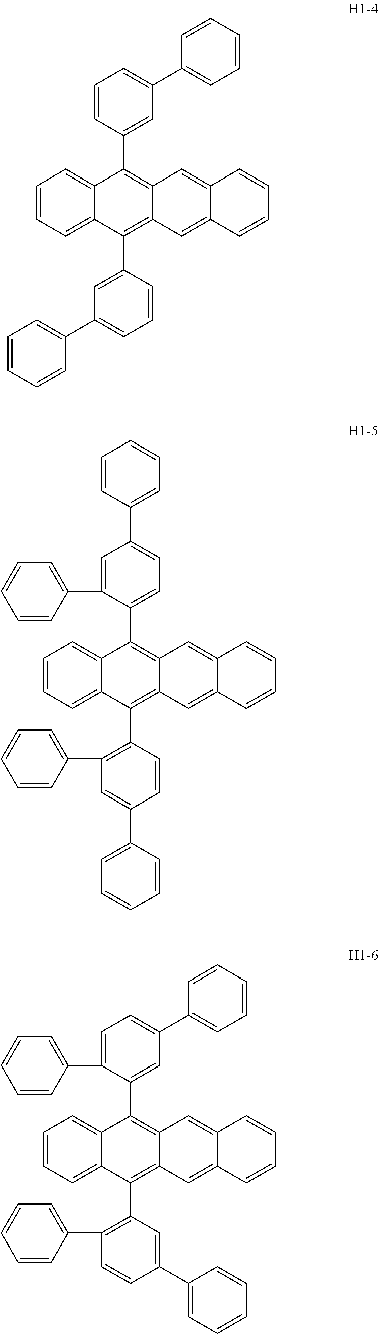


| TABLE 1 | ||
| Evaluation | ||
| Light Emitting Layer | Electron | Light |
| Concentration | Transport Layer | Emitting | Light |
| Light | of Light | Average | Average | Peak | Emitting | ||||||
| Emitting | Host | Emitting | Thickness | Thickness | Wavelength | Power | Voltage | LT80 | |||
| Material | Material | Material [w %] | [nm] | Material | [nm] | [nm] | [mW/cm2] | [V] | [hr] | ||
| Example 1 | D-2 | H1-2 | 4 | 25 | BCP | 80 | 830 | 1.3 | 5.0 | 100 |
| Example 2 | D-2 | H1-5 | 4 | 25 | BCP | 80 | 830 | 1.3 | 5.0 | 130 |
| Example 3 | D-2 | H1-13 | 4 | 25 | BCP | 80 | 830 | 1.5 | 5.1 | 90 |
| Example 4 | D-2 | H1-2 | 1 | 25 | BCP | 80 | 820 | 1.2 | 4.9 | 90 |
| Example 5 | D-2 | H1-2 | 2 | 25 | BCP | 80 | 825 | 1.2 | 5.0 | 100 |
| Example 6 | D-2 | H1-2 | 10 | 25 | BCP | 80 | 835 | 1.0 | 5.2 | 90 |
| Example 7 | D-2 | H1-2 | 4 | 15 | BCP | 90 | 830 | 1.3 | 4.8 | 80 |
| Example 8 | D-2 | H1-2 | 4 | 50 | BCP | 55 | 830 | 1.2 | 5.4 | 120 |
| Example 9 | D-2 | H1-2 | 4 | 70 | |
35 | 830 | 1.2 | 5.7 | 120 |
| Example | D-1 | H1-2 | 4 | 25 | BCP | 80 | 815 | 1.3 | 5.0 | 130 |
| 10 | ||||||||||
| Example | D-3 | H1-2 | 4 | 25 | BCP | 80 | 880 | 0.9 | 5.1 | 110 |
| 11 | ||||||||||
| Reference | D-2 | |
4 | 25 | BCP | 80 | 565, 840 | 0.3 | 6.6 | 20 |
| Example | ||||||||||
Claims (19)


Applications Claiming Priority (2)
| Application Number | Priority Date | Filing Date | Title |
|---|---|---|---|
| JP2011-092427 | 2011-04-18 | ||
| JP2011092427A JP5765034B2 (en) | 2011-04-18 | 2011-04-18 | Thiadiazole compounds, compounds for light emitting devices, light emitting devices, light emitting devices, authentication devices, and electronic devices |
Publications (2)
| Publication Number | Publication Date |
|---|---|
| US20120262057A1 US20120262057A1 (en) | 2012-10-18 |
| US9072150B2 true US9072150B2 (en) | 2015-06-30 |
Family
ID=47005915
Family Applications (1)
| Application Number | Title | Priority Date | Filing Date |
|---|---|---|---|
| US13/445,523 Active 2032-06-09 US9072150B2 (en) | 2011-04-18 | 2012-04-12 | Thiadiazole-based compound, light emitting element compound, light emitting element, light emitting device, authentication device, and electronic apparatus |
Country Status (2)
| Country | Link |
|---|---|
| US (1) | US9072150B2 (en) |
| JP (1) | JP5765034B2 (en) |
Cited By (5)
| Publication number | Priority date | Publication date | Assignee | Title |
|---|---|---|---|---|
| US20150228910A1 (en) * | 2011-08-09 | 2015-08-13 | Seiko Epson Corporation | Thiadiazole, light-emitting element, light-emitting apparatus, authentication apparatus, and electronic device |
| US9324952B2 (en) | 2012-02-28 | 2016-04-26 | Seiko Epson Corporation | Thiadiazole, compound for light-emitting elements, light-emitting element, light-emitting apparatus, authentication apparatus, and electronic device |
| US9401460B2 (en) | 2011-12-28 | 2016-07-26 | Seiko Epson Corporation | Light emitting element |
| US9722184B2 (en) | 2012-10-18 | 2017-08-01 | Seiko Epson Corporation | Thiadiazole, compound for light-emitting elements, light-emitting element, light-emitting apparatus, authentication apparatus, and electronic device |
| US9876177B2 (en) | 2011-04-12 | 2018-01-23 | Seiko Epson Corporation | Thiadiazole-based compound, light emitting element compound, light emitting element, light emitting device, authentication device, and electronic device |
Families Citing this family (17)
| Publication number | Priority date | Publication date | Assignee | Title |
|---|---|---|---|---|
| JP5765034B2 (en) | 2011-04-18 | 2015-08-19 | セイコーエプソン株式会社 | Thiadiazole compounds, compounds for light emitting devices, light emitting devices, light emitting devices, authentication devices, and electronic devices |
| JP5935261B2 (en) * | 2011-08-09 | 2016-06-15 | セイコーエプソン株式会社 | Thiadiazole compounds, compounds for light emitting devices, light emitting devices, light emitting devices, authentication devices, and electronic devices |
| JP5790279B2 (en) * | 2011-08-09 | 2015-10-07 | セイコーエプソン株式会社 | LIGHT EMITTING ELEMENT, LIGHT EMITTING DEVICE, AND ELECTRONIC DEVICE |
| JP6171304B2 (en) * | 2012-10-18 | 2017-08-02 | セイコーエプソン株式会社 | Thiadiazole compounds, compounds for light emitting devices, light emitting devices, light emitting devices, authentication devices, and electronic devices |
| JP5983289B2 (en) * | 2012-10-18 | 2016-08-31 | セイコーエプソン株式会社 | Thiadiazole compounds, compounds for light emitting devices, light emitting devices, light emitting devices, authentication devices, and electronic devices |
| JP6145989B2 (en) * | 2012-10-18 | 2017-06-14 | セイコーエプソン株式会社 | Thiadiazole compounds, compounds for light emitting devices, light emitting devices, light emitting devices, authentication devices, and electronic devices |
| JP2016509621A (en) | 2013-01-04 | 2016-03-31 | 日東電工株式会社 | Highly fluorescent photostable chromophore for wavelength conversion |
| JP6398226B2 (en) * | 2014-02-28 | 2018-10-03 | セイコーエプソン株式会社 | LIGHT EMITTING ELEMENT, LIGHT EMITTING DEVICE, AUTHENTICATION DEVICE, AND ELECTRONIC DEVICE |
| JP6613595B2 (en) | 2014-04-09 | 2019-12-04 | セイコーエプソン株式会社 | LIGHT EMITTING ELEMENT, LIGHT EMITTING DEVICE, AUTHENTICATION DEVICE, AND ELECTRONIC DEVICE |
| JP6459228B2 (en) | 2014-06-02 | 2019-01-30 | セイコーエプソン株式会社 | LIGHT EMITTING DEVICE, ELECTRONIC DEVICE, AND INSPECTION METHOD |
| US10903440B2 (en) * | 2015-02-24 | 2021-01-26 | Semiconductor Energy Laboratory Co., Ltd. | Light-emitting element, light-emitting device, electronic device, and lighting device |
| JP2016006047A (en) * | 2015-06-15 | 2016-01-14 | セイコーエプソン株式会社 | Thiadiazole compound, compound for light emitting element, light emitting element, light emitting device, authentication device and electronic apparatus |
| CN105713016B (en) * | 2016-03-16 | 2018-05-18 | 中节能万润股份有限公司 | A kind of new OLED material and its application |
| JP7043733B2 (en) * | 2017-03-13 | 2022-03-30 | セイコーエプソン株式会社 | Light emitting elements, light emitting devices, light sources, authentication devices and electronic devices |
| JP2018152485A (en) * | 2017-03-14 | 2018-09-27 | セイコーエプソン株式会社 | Light-emitting element, light-emitting device, light source, authentication device and electronic apparatus |
| KR102401011B1 (en) * | 2017-08-16 | 2022-05-24 | 삼성디스플레이 주식회사 | Organic light emitting device and apparatus comprising the same |
| KR20210158460A (en) * | 2020-06-23 | 2021-12-31 | 삼성디스플레이 주식회사 | Organic light emitting device and apparatus including the same |
Citations (75)
| Publication number | Priority date | Publication date | Assignee | Title |
|---|---|---|---|---|
| US4769292A (en) | 1987-03-02 | 1988-09-06 | Eastman Kodak Company | Electroluminescent device with modified thin film luminescent zone |
| JPS63264692A (en) | 1987-03-02 | 1988-11-01 | イーストマン・コダック・カンパニー | Electric field light emitting device having improved membrane light emitting band |
| JPH02255788A (en) | 1989-03-29 | 1990-10-16 | Asahi Chem Ind Co Ltd | Organic el element |
| JPH03792A (en) | 1989-02-17 | 1991-01-07 | Pioneer Electron Corp | Electroluminescent element |
| JPH03791A (en) | 1989-02-20 | 1991-01-07 | Pioneer Electron Corp | Electroluminescent element |
| JPH03162481A (en) | 1989-11-20 | 1991-07-12 | Pioneer Electron Corp | Electroluminescent element |
| JPH03177486A (en) | 1989-12-05 | 1991-08-01 | Pioneer Electron Corp | Electrical field luminescent element |
| JPH0532966A (en) | 1991-07-30 | 1993-02-09 | Sanyo Electric Co Ltd | Organic electrolytically luminescent element |
| JPH05214334A (en) | 1992-02-05 | 1993-08-24 | Konica Corp | Organic thin-film electroluminescent element |
| JPH05258859A (en) | 1991-12-30 | 1993-10-08 | Eastman Kodak Co | Light emitting device and manufacture thereof |
| JPH0673374A (en) | 1992-06-24 | 1994-03-15 | Sumitomo Chem Co Ltd | Organic electroluminescent element |
| JPH0693257A (en) | 1992-09-10 | 1994-04-05 | Kyowa Hakko Kogyo Co Ltd | Organic electroluminescent element |
| JPH06136359A (en) | 1992-10-29 | 1994-05-17 | Sanyo Electric Co Ltd | Electroluminescent element |
| JPH06145146A (en) | 1992-11-06 | 1994-05-24 | Chisso Corp | Oxinate derivative |
| JPH06240246A (en) | 1993-02-17 | 1994-08-30 | Ricoh Co Ltd | Electroluminescent element |
| US5449564A (en) | 1992-10-29 | 1995-09-12 | Sanyo Electric Co., Ltd. | Organic electroluminescent element having improved durability |
| JPH10330295A (en) | 1997-04-04 | 1998-12-15 | Mitsui Chem Inc | Hydrocarbon compound and organic electric field luminous element |
| JPH11233261A (en) | 1997-12-23 | 1999-08-27 | Hewlett Packard Co <Hp> | Organic light emitting diode |
| JP2000091073A (en) | 1998-09-11 | 2000-03-31 | Sony Corp | Organic electroluminescence element |
| JP2001097949A (en) | 1999-09-30 | 2001-04-10 | Idemitsu Kosan Co Ltd | Organic compound and organic electroluminescence element using the same |
| JP2001110570A (en) | 1999-07-30 | 2001-04-20 | Sony Corp | Organic field light emitting element |
| JP2002097465A (en) * | 2000-09-25 | 2002-04-02 | Toyo Ink Mfg Co Ltd | Organic electroluminescence element material and organic electroluminescence element obtained using the same |
| US20030008172A1 (en) | 2001-04-10 | 2003-01-09 | Mario Leclerc | Conjugated polycarbazole derivatives in Organic Light Emitting Diodes |
| US20030027016A1 (en) | 2000-04-21 | 2003-02-06 | Tdk Corporation | Organic EL device |
| JP2003055652A (en) | 2001-06-06 | 2003-02-26 | Sanyo Electric Co Ltd | Organic electroluminescent element and luminescent material |
| JP2003109760A (en) | 2001-09-28 | 2003-04-11 | Canon Inc | Organic light emitting element |
| WO2003095445A1 (en) | 2002-05-07 | 2003-11-20 | Lg Chem, Ltd. | New organic compounds for electroluminescence and organic electroluminescent devices using the same |
| JP2004002297A (en) | 2002-04-11 | 2004-01-08 | Idemitsu Kosan Co Ltd | New nitrogen-containing heterocyclic derivative and organic electroluminescent element using the same |
| US20040018382A1 (en) | 2002-07-29 | 2004-01-29 | Crosslink Polymer Research | Electroluminescent device and methods for its production and use |
| WO2004058911A2 (en) | 2002-12-23 | 2004-07-15 | Covion Organic Semiconductors Gmbh | Organic electroluminescent element |
| JP2005063938A (en) | 2003-05-09 | 2005-03-10 | Fuji Photo Film Co Ltd | Organic electroluminescent element |
| JP2006045398A (en) | 2004-08-06 | 2006-02-16 | Toyo Ink Mfg Co Ltd | Material for use in organic electroluminescent device, and organic electroluminescent device using the material |
| US20060154105A1 (en) | 2003-01-10 | 2006-07-13 | Hiroshi Yamamoto | Nitrogenous heterocyclic derivative and organic elecrtroluminescent element employing the same |
| US20070077453A1 (en) | 2005-10-04 | 2007-04-05 | Fujifilm Corporation | Organic electroluminescent element |
| JP2007115626A (en) | 2005-10-24 | 2007-05-10 | Seiko Epson Corp | Organic el apparatus |
| US20070285005A1 (en) | 2004-03-31 | 2007-12-13 | Fuji Photo Film., Ltd. | Organic Electroluminescent Element and Organic Electroluminescent Display |
| US20080061681A1 (en) | 2006-09-11 | 2008-03-13 | The Trustees Of Princeton University | Near-infrared emitting organic compounds and organic devices using the same |
| US20080067479A1 (en) | 2006-09-14 | 2008-03-20 | Fujifilm Corporation | Near-infrared-absorbing material and near-infrared-absorbing filter |
| JP2008069100A (en) | 2006-09-13 | 2008-03-27 | Tdk Corp | Compound for organic el element and organic el element |
| WO2008069322A1 (en) | 2006-12-08 | 2008-06-12 | National Institute Of Advanced Industrial Science And Technology | Metal coordination compound and light-emitting material using the same |
| US20080230123A1 (en) | 2007-03-12 | 2008-09-25 | Fujifilm Corporation | Photoelectric conversion element and solid-state imaging device |
| JP2009016693A (en) | 2007-07-07 | 2009-01-22 | Idemitsu Kosan Co Ltd | Host material, and organic el element |
| JP2009049094A (en) | 2007-08-16 | 2009-03-05 | Sony Corp | Organic electroluminescent element, and display device |
| US20090079335A1 (en) | 2007-09-21 | 2009-03-26 | Seiko Epson Corporation | Light-emitting device, display, and electronic apparatus |
| US20090091250A1 (en) | 2007-10-03 | 2009-04-09 | Seiko Epson Corporation | Light-emitting device, display, and electronic apparatus |
| US20090115348A1 (en) * | 2000-08-28 | 2009-05-07 | Semiconductor Energy Laboratory Co., Ltd. | Light emitting device |
| US20090243476A1 (en) | 2008-03-28 | 2009-10-01 | Semiconductor Energy Laboratory Co., Ltd. | Acenaphthoquinoxaline Derivative, Light-Emitting Element, Light-Emitting Device, and Electronic Device |
| US20090261360A1 (en) | 2008-01-29 | 2009-10-22 | Seiko Epson Corporation | Light-emitting element, display device, and electronic apparatus |
| US7632579B2 (en) | 2000-07-17 | 2009-12-15 | Fujifilm Corporation | Light emitting element and azole compound |
| US7714099B2 (en) | 2004-10-15 | 2010-05-11 | Hitachi Chemical Co., Ltd. | Luminescent compositions and their uses |
| US20100133434A1 (en) | 2008-11-28 | 2010-06-03 | National Chiao Tung University | Organic semiconductor infrared distance sensing apparatus and organic infrared emitting apparatus thereof |
| US20100155694A1 (en) | 2004-12-09 | 2010-06-24 | 3M Innovative Properties Company | Adapting short-wavelength led's for polychromatic, broadband, or "white" emission |
| JP2010147179A (en) | 2008-12-17 | 2010-07-01 | Sumitomo Chemical Co Ltd | Organic electroluminescent element |
| US20100237338A1 (en) | 2009-03-23 | 2010-09-23 | Seiko Epson Corporation | Light-emitting element, light-emitting device, display, and electronic apparatus |
| US20100237990A1 (en) | 2009-03-12 | 2010-09-23 | Seiko Epson Corporation | Biological information acquiring apparatus, biological information acquiring method and biometric authentication apparatus |
| US20100244671A1 (en) | 2009-03-31 | 2010-09-30 | Semiconductor Energy Laboratory Co., Ltd. | Quinoxaline Derivative, and Light-Emitting Element, Light-Emitting Device, Lighting Device, and Electronic Device Using Quinoxaline Derivative |
| US20100244679A1 (en) | 2009-03-26 | 2010-09-30 | Seiko Epson Corporation | Light-emitting element, light-emitting apparatus, display apparatus, and electronic device |
| US7902542B2 (en) | 2006-06-14 | 2011-03-08 | 3M Innovative Properties Company | Adapted LED device with re-emitting semiconductor construction |
| US7919773B2 (en) | 2006-03-20 | 2011-04-05 | Semiconductor Energy Laboratory Co., Ltd. | Aromatic amine compound, and light-emitting element, light-emitting device, and electronic appliance using the aromatic amine compound |
| US20110087034A1 (en) | 2008-02-06 | 2011-04-14 | Sumitomo Chemical Company Limited | Organic Semiconductor Material |
| US8039128B2 (en) | 2007-05-28 | 2011-10-18 | Canon Kabushiki Kaisha | Fluorene compound, organic light emitting device and display device using the fluorene compound |
| US20110253988A1 (en) | 2010-04-16 | 2011-10-20 | Basf Se | Bridged benzimidazole-carbene complexes and use thereof in oleds |
| US20110279020A1 (en) | 2010-04-20 | 2011-11-17 | Idemitsu Kosan Co., Ltd. | Biscarbazole Derivative, Material for Organic Electroluminescence Device and Organic Electroluminescence Device Using The Same |
| US20110303901A1 (en) | 2010-06-15 | 2011-12-15 | Chien-Hong Cheng | 6H-INDOLO[2,3-b]QUINOXALINE DERIVATIVES AND ORGANIC LIGHT EMITTING DIODE USING THE SAME |
| US20120056213A1 (en) | 2010-09-06 | 2012-03-08 | Seiko Epson Corporation | Light-emitting element, light-emitting device, display device, and electronic apparatus |
| US20120091923A1 (en) | 2008-12-11 | 2012-04-19 | Osram Opto Semiconductors Gmbh | Organic-Light-Emitting Diode and Luminaire |
| US20120262057A1 (en) | 2011-04-18 | 2012-10-18 | Seiko Epson Corporation | Thiadiazole-based compound, light emitting element compound, light emitting element, light emitting device, authentication device, and electronic apparatus |
| US20120267615A1 (en) | 2011-04-12 | 2012-10-25 | Seiko Epson Corporation | Thiadiazole-based compound, light emitting element compound, light emitting element, light emitting device, authentication device, and electronic device |
| US20130009909A1 (en) | 2011-07-08 | 2013-01-10 | Semiconductor Energy Laboratory Co., Ltd. | Display Device |
| US20130032791A1 (en) | 2011-06-24 | 2013-02-07 | Bazan Guillermo C | Conjugated polymers having an imine group at the intrachain electron donor bridgehead position useful in electronic devices |
| US20130037785A1 (en) * | 2011-08-09 | 2013-02-14 | Seiko Epson Corporation | Light emitting element, light emitting device, and electronic device |
| US20130037784A1 (en) | 2011-08-09 | 2013-02-14 | Seiko Epson Corporation | Thiadiazole, light-emitting element, light-emitting apparatus, authentication apparatus, and electronic device |
| US20130099209A1 (en) | 2010-03-31 | 2013-04-25 | Osram Opto Semiconductors Gmbh | Dopant for a Hole Conductor Layer for Organic Semiconductor Components, and Use Thereof |
| US20130168654A1 (en) * | 2011-12-28 | 2013-07-04 | Seiko Epson Corporation | Light emitting element, light emitting device and electronic apparatus |
| US20130221334A1 (en) | 2012-02-28 | 2013-08-29 | Seiko Epson Corporation | Thiadiazole, compound for light-emitting elements, light-emitting element, light-emitting apparatus, authentication apparatus, and electronic device |
Family Cites Families (1)
| Publication number | Priority date | Publication date | Assignee | Title |
|---|---|---|---|---|
| JP3579730B2 (en) * | 1995-06-28 | 2004-10-20 | チッソ株式会社 | Organic electroluminescent device using quinoxaline derivative |
-
2011
- 2011-04-18 JP JP2011092427A patent/JP5765034B2/en active Active
-
2012
- 2012-04-12 US US13/445,523 patent/US9072150B2/en active Active
Patent Citations (90)
| Publication number | Priority date | Publication date | Assignee | Title |
|---|---|---|---|---|
| JPS63264692A (en) | 1987-03-02 | 1988-11-01 | イーストマン・コダック・カンパニー | Electric field light emitting device having improved membrane light emitting band |
| EP0281381B1 (en) | 1987-03-02 | 1992-07-15 | EASTMAN KODAK COMPANY (a New Jersey corporation) | Electroluminescent device with modified thin film luminescent zone |
| US4769292A (en) | 1987-03-02 | 1988-09-06 | Eastman Kodak Company | Electroluminescent device with modified thin film luminescent zone |
| JPH03792A (en) | 1989-02-17 | 1991-01-07 | Pioneer Electron Corp | Electroluminescent element |
| US5104740A (en) | 1989-02-17 | 1992-04-14 | Pioneer Electronic Corporation | Electroluminescent element |
| JPH03791A (en) | 1989-02-20 | 1991-01-07 | Pioneer Electron Corp | Electroluminescent element |
| JPH02255788A (en) | 1989-03-29 | 1990-10-16 | Asahi Chem Ind Co Ltd | Organic el element |
| JPH03162481A (en) | 1989-11-20 | 1991-07-12 | Pioneer Electron Corp | Electroluminescent element |
| JPH03177486A (en) | 1989-12-05 | 1991-08-01 | Pioneer Electron Corp | Electrical field luminescent element |
| JPH0532966A (en) | 1991-07-30 | 1993-02-09 | Sanyo Electric Co Ltd | Organic electrolytically luminescent element |
| US5294869A (en) | 1991-12-30 | 1994-03-15 | Eastman Kodak Company | Organic electroluminescent multicolor image display device |
| JPH05258859A (en) | 1991-12-30 | 1993-10-08 | Eastman Kodak Co | Light emitting device and manufacture thereof |
| JPH05214334A (en) | 1992-02-05 | 1993-08-24 | Konica Corp | Organic thin-film electroluminescent element |
| JPH0673374A (en) | 1992-06-24 | 1994-03-15 | Sumitomo Chem Co Ltd | Organic electroluminescent element |
| JPH0693257A (en) | 1992-09-10 | 1994-04-05 | Kyowa Hakko Kogyo Co Ltd | Organic electroluminescent element |
| JPH06136359A (en) | 1992-10-29 | 1994-05-17 | Sanyo Electric Co Ltd | Electroluminescent element |
| US5449564A (en) | 1992-10-29 | 1995-09-12 | Sanyo Electric Co., Ltd. | Organic electroluminescent element having improved durability |
| JPH06145146A (en) | 1992-11-06 | 1994-05-24 | Chisso Corp | Oxinate derivative |
| JPH06240246A (en) | 1993-02-17 | 1994-08-30 | Ricoh Co Ltd | Electroluminescent element |
| JPH10330295A (en) | 1997-04-04 | 1998-12-15 | Mitsui Chem Inc | Hydrocarbon compound and organic electric field luminous element |
| JPH11233261A (en) | 1997-12-23 | 1999-08-27 | Hewlett Packard Co <Hp> | Organic light emitting diode |
| US6004685A (en) | 1997-12-23 | 1999-12-21 | Hewlett-Packard Company & The Board Of Regents Of The University Of Texas System | LED doped with periflanthene for efficient red emission |
| JP2000091073A (en) | 1998-09-11 | 2000-03-31 | Sony Corp | Organic electroluminescence element |
| JP2001110570A (en) | 1999-07-30 | 2001-04-20 | Sony Corp | Organic field light emitting element |
| US6680131B1 (en) | 1999-07-30 | 2004-01-20 | Sony Corporation | Organic electroluminescent device |
| JP2001097949A (en) | 1999-09-30 | 2001-04-10 | Idemitsu Kosan Co Ltd | Organic compound and organic electroluminescence element using the same |
| US20030027016A1 (en) | 2000-04-21 | 2003-02-06 | Tdk Corporation | Organic EL device |
| US7632579B2 (en) | 2000-07-17 | 2009-12-15 | Fujifilm Corporation | Light emitting element and azole compound |
| US20090115348A1 (en) * | 2000-08-28 | 2009-05-07 | Semiconductor Energy Laboratory Co., Ltd. | Light emitting device |
| JP2002097465A (en) * | 2000-09-25 | 2002-04-02 | Toyo Ink Mfg Co Ltd | Organic electroluminescence element material and organic electroluminescence element obtained using the same |
| US20030008172A1 (en) | 2001-04-10 | 2003-01-09 | Mario Leclerc | Conjugated polycarbazole derivatives in Organic Light Emitting Diodes |
| US20050079381A1 (en) | 2001-06-06 | 2005-04-14 | Yuji Hamada | Organic electroluminescene device and luminance material |
| JP2003055652A (en) | 2001-06-06 | 2003-02-26 | Sanyo Electric Co Ltd | Organic electroluminescent element and luminescent material |
| JP2003109760A (en) | 2001-09-28 | 2003-04-11 | Canon Inc | Organic light emitting element |
| JP2004002297A (en) | 2002-04-11 | 2004-01-08 | Idemitsu Kosan Co Ltd | New nitrogen-containing heterocyclic derivative and organic electroluminescent element using the same |
| WO2003095445A1 (en) | 2002-05-07 | 2003-11-20 | Lg Chem, Ltd. | New organic compounds for electroluminescence and organic electroluminescent devices using the same |
| JP2005531552A (en) | 2002-05-07 | 2005-10-20 | エルジー・ケム・リミテッド | New organic light emitting compound and organic light emitting device using the same |
| US20040018382A1 (en) | 2002-07-29 | 2004-01-29 | Crosslink Polymer Research | Electroluminescent device and methods for its production and use |
| US20060063027A1 (en) | 2002-12-23 | 2006-03-23 | Covion Organic Semiconductors Gmbh | Organic electroluminescent element |
| JP2006511939A (en) | 2002-12-23 | 2006-04-06 | コビオン・オーガニック・セミコンダクターズ・ゲーエムベーハー | Organic electroluminescence device |
| WO2004058911A2 (en) | 2002-12-23 | 2004-07-15 | Covion Organic Semiconductors Gmbh | Organic electroluminescent element |
| US20060154105A1 (en) | 2003-01-10 | 2006-07-13 | Hiroshi Yamamoto | Nitrogenous heterocyclic derivative and organic elecrtroluminescent element employing the same |
| JP2005063938A (en) | 2003-05-09 | 2005-03-10 | Fuji Photo Film Co Ltd | Organic electroluminescent element |
| US20070285005A1 (en) | 2004-03-31 | 2007-12-13 | Fuji Photo Film., Ltd. | Organic Electroluminescent Element and Organic Electroluminescent Display |
| JP2006045398A (en) | 2004-08-06 | 2006-02-16 | Toyo Ink Mfg Co Ltd | Material for use in organic electroluminescent device, and organic electroluminescent device using the material |
| US7714099B2 (en) | 2004-10-15 | 2010-05-11 | Hitachi Chemical Co., Ltd. | Luminescent compositions and their uses |
| US20100155694A1 (en) | 2004-12-09 | 2010-06-24 | 3M Innovative Properties Company | Adapting short-wavelength led's for polychromatic, broadband, or "white" emission |
| US20070077453A1 (en) | 2005-10-04 | 2007-04-05 | Fujifilm Corporation | Organic electroluminescent element |
| JP2007115626A (en) | 2005-10-24 | 2007-05-10 | Seiko Epson Corp | Organic el apparatus |
| US7919773B2 (en) | 2006-03-20 | 2011-04-05 | Semiconductor Energy Laboratory Co., Ltd. | Aromatic amine compound, and light-emitting element, light-emitting device, and electronic appliance using the aromatic amine compound |
| US7902542B2 (en) | 2006-06-14 | 2011-03-08 | 3M Innovative Properties Company | Adapted LED device with re-emitting semiconductor construction |
| US20080061681A1 (en) | 2006-09-11 | 2008-03-13 | The Trustees Of Princeton University | Near-infrared emitting organic compounds and organic devices using the same |
| JP2008069100A (en) | 2006-09-13 | 2008-03-27 | Tdk Corp | Compound for organic el element and organic el element |
| US20080067479A1 (en) | 2006-09-14 | 2008-03-20 | Fujifilm Corporation | Near-infrared-absorbing material and near-infrared-absorbing filter |
| US20100317858A1 (en) | 2006-12-08 | 2010-12-16 | National Institute Of Advance Industrial Science And Technology | Metal coordination compound and light-emitting material containing the same |
| WO2008069322A1 (en) | 2006-12-08 | 2008-06-12 | National Institute Of Advanced Industrial Science And Technology | Metal coordination compound and light-emitting material using the same |
| US20080230123A1 (en) | 2007-03-12 | 2008-09-25 | Fujifilm Corporation | Photoelectric conversion element and solid-state imaging device |
| US8039128B2 (en) | 2007-05-28 | 2011-10-18 | Canon Kabushiki Kaisha | Fluorene compound, organic light emitting device and display device using the fluorene compound |
| JP2009016693A (en) | 2007-07-07 | 2009-01-22 | Idemitsu Kosan Co Ltd | Host material, and organic el element |
| JP2009049094A (en) | 2007-08-16 | 2009-03-05 | Sony Corp | Organic electroluminescent element, and display device |
| US20090079335A1 (en) | 2007-09-21 | 2009-03-26 | Seiko Epson Corporation | Light-emitting device, display, and electronic apparatus |
| US20090091250A1 (en) | 2007-10-03 | 2009-04-09 | Seiko Epson Corporation | Light-emitting device, display, and electronic apparatus |
| US7960912B2 (en) | 2007-10-03 | 2011-06-14 | Seiko Epson Corporation | Light-emitting device that includes a plurality of light-emitting layers stacked on top of each other, display, and electronic apparatus |
| US7947992B2 (en) | 2008-01-29 | 2011-05-24 | Seiko Epson Corporation | Light-emitting element, display device, and electronic apparatus |
| US20090261360A1 (en) | 2008-01-29 | 2009-10-22 | Seiko Epson Corporation | Light-emitting element, display device, and electronic apparatus |
| US20110087034A1 (en) | 2008-02-06 | 2011-04-14 | Sumitomo Chemical Company Limited | Organic Semiconductor Material |
| JP2009256343A (en) | 2008-03-28 | 2009-11-05 | Semiconductor Energy Lab Co Ltd | Acenaphthoquinoxaline derivative, light-emitting element, light-emitting device, and electronic equipment |
| US20090243476A1 (en) | 2008-03-28 | 2009-10-01 | Semiconductor Energy Laboratory Co., Ltd. | Acenaphthoquinoxaline Derivative, Light-Emitting Element, Light-Emitting Device, and Electronic Device |
| US20100133434A1 (en) | 2008-11-28 | 2010-06-03 | National Chiao Tung University | Organic semiconductor infrared distance sensing apparatus and organic infrared emitting apparatus thereof |
| US20120091923A1 (en) | 2008-12-11 | 2012-04-19 | Osram Opto Semiconductors Gmbh | Organic-Light-Emitting Diode and Luminaire |
| JP2010147179A (en) | 2008-12-17 | 2010-07-01 | Sumitomo Chemical Co Ltd | Organic electroluminescent element |
| US20100237990A1 (en) | 2009-03-12 | 2010-09-23 | Seiko Epson Corporation | Biological information acquiring apparatus, biological information acquiring method and biometric authentication apparatus |
| US20100237338A1 (en) | 2009-03-23 | 2010-09-23 | Seiko Epson Corporation | Light-emitting element, light-emitting device, display, and electronic apparatus |
| US20100244679A1 (en) | 2009-03-26 | 2010-09-30 | Seiko Epson Corporation | Light-emitting element, light-emitting apparatus, display apparatus, and electronic device |
| JP2010254674A (en) | 2009-03-31 | 2010-11-11 | Semiconductor Energy Lab Co Ltd | Quinoxaline derivative, light emitting element employing the same, light emitting apparatus, illumination apparatus, and electronic equipment |
| US20100244671A1 (en) | 2009-03-31 | 2010-09-30 | Semiconductor Energy Laboratory Co., Ltd. | Quinoxaline Derivative, and Light-Emitting Element, Light-Emitting Device, Lighting Device, and Electronic Device Using Quinoxaline Derivative |
| US20130099209A1 (en) | 2010-03-31 | 2013-04-25 | Osram Opto Semiconductors Gmbh | Dopant for a Hole Conductor Layer for Organic Semiconductor Components, and Use Thereof |
| US20110253988A1 (en) | 2010-04-16 | 2011-10-20 | Basf Se | Bridged benzimidazole-carbene complexes and use thereof in oleds |
| US20110279020A1 (en) | 2010-04-20 | 2011-11-17 | Idemitsu Kosan Co., Ltd. | Biscarbazole Derivative, Material for Organic Electroluminescence Device and Organic Electroluminescence Device Using The Same |
| US20110303901A1 (en) | 2010-06-15 | 2011-12-15 | Chien-Hong Cheng | 6H-INDOLO[2,3-b]QUINOXALINE DERIVATIVES AND ORGANIC LIGHT EMITTING DIODE USING THE SAME |
| US20120056213A1 (en) | 2010-09-06 | 2012-03-08 | Seiko Epson Corporation | Light-emitting element, light-emitting device, display device, and electronic apparatus |
| US20120267615A1 (en) | 2011-04-12 | 2012-10-25 | Seiko Epson Corporation | Thiadiazole-based compound, light emitting element compound, light emitting element, light emitting device, authentication device, and electronic device |
| US20120262057A1 (en) | 2011-04-18 | 2012-10-18 | Seiko Epson Corporation | Thiadiazole-based compound, light emitting element compound, light emitting element, light emitting device, authentication device, and electronic apparatus |
| US20130032791A1 (en) | 2011-06-24 | 2013-02-07 | Bazan Guillermo C | Conjugated polymers having an imine group at the intrachain electron donor bridgehead position useful in electronic devices |
| US20130009909A1 (en) | 2011-07-08 | 2013-01-10 | Semiconductor Energy Laboratory Co., Ltd. | Display Device |
| US20130037785A1 (en) * | 2011-08-09 | 2013-02-14 | Seiko Epson Corporation | Light emitting element, light emitting device, and electronic device |
| US20130037784A1 (en) | 2011-08-09 | 2013-02-14 | Seiko Epson Corporation | Thiadiazole, light-emitting element, light-emitting apparatus, authentication apparatus, and electronic device |
| US20130168654A1 (en) * | 2011-12-28 | 2013-07-04 | Seiko Epson Corporation | Light emitting element, light emitting device and electronic apparatus |
| US8803138B2 (en) | 2011-12-28 | 2014-08-12 | Seiko Epson Corporation | Light emitting element, light emitting device and electronic apparatus |
| US20130221334A1 (en) | 2012-02-28 | 2013-08-29 | Seiko Epson Corporation | Thiadiazole, compound for light-emitting elements, light-emitting element, light-emitting apparatus, authentication apparatus, and electronic device |
Non-Patent Citations (20)
| Title |
|---|
| Apr. 22, 2015 Office Action issued in U.S. Appl. No. 13/773,033. |
| Aug. 15, 2014 Office Action issued in U.S. Appl. No. 13/564,384. |
| Aug. 21, 2014 Office Action issued in U.S. Appl. No. 13/564,376. |
| Du et al., "Efficient Non-Doped Near Infrared Organic Light-Emitting Devices Based on Fluorophores with Aggregation-Induced Emission Enhancement," Chemistry of Materials, vol. 24 (2012) pp. 2178-2185. |
| Jan. 22, 2015 Office Action issued in U.S. Appl. No. 13/564,384. |
| Jeff D. Debad et al.; Dibenzotetraphenylperiflanthene: Synthesis, Photophysical Properties, and Electrogenerated Chemiluminescence; Journal American Chemical Society; 1996; vol. 118; pp. 2374-2379. |
| Kajii et al., "Visible to Near-Infrared Organic Light-Emitting Diodes Using Phosphorescent Materials by Solution Process," Thin Solid Films, vol. 518 (2009) pp. 551-554. |
| Machine English translation of JP 2002-097465 A. Jan. 3, 2014. * |
| Mar. 26, 2014 Notice of Allowance issued in U.S. Appl. No. 13/727,339. |
| Mitsuo Kawabe et al.; Electroluminescence of Green Light Region in Doped Anthracene; Japan Journal Appl. Phys. vol. 10; (1971); pp. 527-529. |
| Oct. 3, 2014 Office Action issued in U.S. Appl. No. 14/319,410. |
| Pending U.S. Appl. No. 13/444,107, filed on Apr. 11, 2012,. |
| Pending U.S. Appl. No. 13/564,376, filed on Aug. 1, 2012. |
| Pending U.S. Appl. No. 13/564,384, filed on Aug. 1, 2012. |
| Pending U.S. Appl. No. 13/773,033, filed on Feb. 21, 2013. |
| Pending U.S. Appl. No. 14/055,241, filed on Oct. 16, 2013. |
| Pending U.S. Appl. No. 14/319,410, filed on Jun. 30, 2014. |
| Qian, et al., "Synthesis and Application of Thiadiazoloquinoxaline-Containing Chromophores as Dopants for Efficient Near-Infrared Organic Light-Emitting Diodes," J. Phys. Chem. C, vol. 113 (2009) pp. 1589-1595. |
| U.S. Appl. No. 14/693,484, filed Apr. 22, 2015 in the name of Yamamoto et al. |
| U.S. Appl. No. 14/700,751, filed Apr. 30, 2015 in the name of Fujita et al. |
Cited By (6)
| Publication number | Priority date | Publication date | Assignee | Title |
|---|---|---|---|---|
| US9876177B2 (en) | 2011-04-12 | 2018-01-23 | Seiko Epson Corporation | Thiadiazole-based compound, light emitting element compound, light emitting element, light emitting device, authentication device, and electronic device |
| US20150228910A1 (en) * | 2011-08-09 | 2015-08-13 | Seiko Epson Corporation | Thiadiazole, light-emitting element, light-emitting apparatus, authentication apparatus, and electronic device |
| US9741940B2 (en) * | 2011-08-09 | 2017-08-22 | Seiko Epson Corporation | Thiadiazole, light-emitting element, light-emitting apparatus, authentication apparatus, and electronic device |
| US9401460B2 (en) | 2011-12-28 | 2016-07-26 | Seiko Epson Corporation | Light emitting element |
| US9324952B2 (en) | 2012-02-28 | 2016-04-26 | Seiko Epson Corporation | Thiadiazole, compound for light-emitting elements, light-emitting element, light-emitting apparatus, authentication apparatus, and electronic device |
| US9722184B2 (en) | 2012-10-18 | 2017-08-01 | Seiko Epson Corporation | Thiadiazole, compound for light-emitting elements, light-emitting element, light-emitting apparatus, authentication apparatus, and electronic device |
Also Published As
| Publication number | Publication date |
|---|---|
| US20120262057A1 (en) | 2012-10-18 |
| JP5765034B2 (en) | 2015-08-19 |
| JP2012224567A (en) | 2012-11-15 |
Similar Documents
| Publication | Publication Date | Title |
|---|---|---|
| US9072150B2 (en) | Thiadiazole-based compound, light emitting element compound, light emitting element, light emitting device, authentication device, and electronic apparatus | |
| TWI586669B (en) | Thiadiazole, light-emitting element, light-emitting apparatus, authentication apparatus, and electronic device | |
| US20170365793A1 (en) | Thiadiazole-based compound, light emitting element compound, light emitting element, light emitting device, authentication device, and electronic device | |
| JP5682429B2 (en) | Thiadiazole compounds, compounds for light emitting devices, light emitting devices, light emitting devices, authentication devices, and electronic devices | |
| JP6149377B2 (en) | Light emitting element, light emitting device, authentication device, and electronic device | |
| JP6693053B2 (en) | Light emitting element, light emitting device, authentication device, and electronic device | |
| JP7043733B2 (en) | Light emitting elements, light emitting devices, light sources, authentication devices and electronic devices | |
| JP5982867B2 (en) | Thiadiazole compounds, compounds for light emitting devices, light emitting devices, light emitting devices, authentication devices, and electronic devices | |
| JP6885065B2 (en) | Compounds, compounds for light emitting elements, light emitting elements, light emitting devices, light sources, authentication devices and electronic devices | |
| JP5879804B2 (en) | LIGHT EMITTING ELEMENT, LIGHT EMITTING DEVICE, AUTHENTICATION DEVICE, AND ELECTRONIC DEVICE | |
| JP6331779B2 (en) | LIGHT EMITTING ELEMENT, LIGHT EMITTING DEVICE, AUTHENTICATION DEVICE, AND ELECTRONIC DEVICE | |
| JP5935261B2 (en) | Thiadiazole compounds, compounds for light emitting devices, light emitting devices, light emitting devices, authentication devices, and electronic devices | |
| JP6142498B2 (en) | Light emitting element, light emitting device, authentication device, and electronic device | |
| JP6003087B2 (en) | Light emitting element, light emitting device, authentication device, and electronic device | |
| JP6145989B2 (en) | Thiadiazole compounds, compounds for light emitting devices, light emitting devices, light emitting devices, authentication devices, and electronic devices | |
| JP5983289B2 (en) | Thiadiazole compounds, compounds for light emitting devices, light emitting devices, light emitting devices, authentication devices, and electronic devices | |
| JP5799560B2 (en) | LIGHT EMITTING ELEMENT, LIGHT EMITTING DEVICE, AUTHENTICATION DEVICE, AND ELECTRONIC DEVICE | |
| JP6171304B2 (en) | Thiadiazole compounds, compounds for light emitting devices, light emitting devices, light emitting devices, authentication devices, and electronic devices | |
| JP6191714B2 (en) | Light emitting element, light emitting device, authentication device, and electronic device | |
| JP5987885B2 (en) | Electronics | |
| JP5879727B2 (en) | LIGHT EMITTING ELEMENT, LIGHT EMITTING DEVICE, AUTHENTICATION DEVICE, AND ELECTRONIC DEVICE | |
| JP6885066B2 (en) | Compounds, compounds for light emitting elements, light emitting elements, light emitting devices, light sources, authentication devices and electronic devices | |
| JP5831030B2 (en) | LIGHT EMITTING ELEMENT, LIGHT EMITTING DEVICE, AUTHENTICATION DEVICE, AND ELECTRONIC DEVICE | |
| JP2016006047A (en) | Thiadiazole compound, compound for light emitting element, light emitting element, light emitting device, authentication device and electronic apparatus |
Legal Events
| Date | Code | Title | Description |
|---|---|---|---|
| AS | Assignment |
Owner name: SEIKO EPSON CORPORATION, JAPAN Free format text: ASSIGNMENT OF ASSIGNORS INTEREST;ASSIGNORS:FUJITA, TETSUJI;YAMAMOTO, HIDETOSHI;REEL/FRAME:028047/0364 Effective date: 20120323 |
|
| STCF | Information on status: patent grant |
Free format text: PATENTED CASE |
|
| MAFP | Maintenance fee payment |
Free format text: PAYMENT OF MAINTENANCE FEE, 4TH YEAR, LARGE ENTITY (ORIGINAL EVENT CODE: M1551); ENTITY STATUS OF PATENT OWNER: LARGE ENTITY Year of fee payment: 4 |
|
| MAFP | Maintenance fee payment |
Free format text: PAYMENT OF MAINTENANCE FEE, 8TH YEAR, LARGE ENTITY (ORIGINAL EVENT CODE: M1552); ENTITY STATUS OF PATENT OWNER: LARGE ENTITY Year of fee payment: 8 |