US9101005B2 - Package of environmental sensitive element - Google Patents

Package of environmental sensitive element Download PDF

Info

Publication number
US9101005B2
US9101005B2 US13/867,136 US201313867136A US9101005B2 US 9101005 B2 US9101005 B2 US 9101005B2 US 201313867136 A US201313867136 A US 201313867136A US 9101005 B2 US9101005 B2 US 9101005B2
Authority
US
United States
Prior art keywords
package
flexible
thin film
sensitive element
sacrificial
Prior art date
Legal status (The legal status is an assumption and is not a legal conclusion. Google has not performed a legal analysis and makes no representation as to the accuracy of the status listed.)
Active, expires
Application number
US13/867,136
Other versions
US20130229108A1 (en
Inventor
Kuang-Jung Chen
Current Assignee (The listed assignees may be inaccurate. Google has not performed a legal analysis and makes no representation or warranty as to the accuracy of the list.)
Hannstar Display Corp
Original Assignee
Industrial Technology Research Institute ITRI
Priority date (The priority date is an assumption and is not a legal conclusion. Google has not performed a legal analysis and makes no representation as to the accuracy of the date listed.)
Filing date
Publication date
Priority claimed from TW098131092A external-priority patent/TWI407535B/en
Application filed by Industrial Technology Research Institute ITRI filed Critical Industrial Technology Research Institute ITRI
Priority to US13/867,136 priority Critical patent/US9101005B2/en
Assigned to INDUSTRIAL TECHNOLOGY RESEARCH INSTITUTE reassignment INDUSTRIAL TECHNOLOGY RESEARCH INSTITUTE ASSIGNMENT OF ASSIGNORS INTEREST (SEE DOCUMENT FOR DETAILS). Assignors: CHEN, KUANG-JUNG
Publication of US20130229108A1 publication Critical patent/US20130229108A1/en
Priority to US14/730,253 priority patent/US9224700B2/en
Application granted granted Critical
Publication of US9101005B2 publication Critical patent/US9101005B2/en
Priority to US14/948,394 priority patent/US9660218B2/en
Assigned to HANNSTAR DISPLAY CORPORATION reassignment HANNSTAR DISPLAY CORPORATION ASSIGNMENT OF ASSIGNORS INTEREST (SEE DOCUMENT FOR DETAILS). Assignors: INDUSTRIAL TECHNOLOGY RESEARCH INSTITUTE
Active legal-status Critical Current
Adjusted expiration legal-status Critical

Links

Images

Classifications

    • HELECTRICITY
    • H01ELECTRIC ELEMENTS
    • H01LSEMICONDUCTOR DEVICES NOT COVERED BY CLASS H10
    • H01L23/00Details of semiconductor or other solid state devices
    • H01L23/564Details not otherwise provided for, e.g. protection against moisture
    • HELECTRICITY
    • H05ELECTRIC TECHNIQUES NOT OTHERWISE PROVIDED FOR
    • H05BELECTRIC HEATING; ELECTRIC LIGHT SOURCES NOT OTHERWISE PROVIDED FOR; CIRCUIT ARRANGEMENTS FOR ELECTRIC LIGHT SOURCES, IN GENERAL
    • H05B33/00Electroluminescent light sources
    • H05B33/02Details
    • H05B33/04Sealing arrangements, e.g. against humidity
    • HELECTRICITY
    • H01ELECTRIC ELEMENTS
    • H01LSEMICONDUCTOR DEVICES NOT COVERED BY CLASS H10
    • H01L23/00Details of semiconductor or other solid state devices
    • H01L23/562Protection against mechanical damage
    • H01L51/0097
    • H01L51/5253
    • H01L51/5256
    • HELECTRICITY
    • H10SEMICONDUCTOR DEVICES; ELECTRIC SOLID-STATE DEVICES NOT OTHERWISE PROVIDED FOR
    • H10KORGANIC ELECTRIC SOLID-STATE DEVICES
    • H10K50/00Organic light-emitting devices
    • H10K50/80Constructional details
    • HELECTRICITY
    • H10SEMICONDUCTOR DEVICES; ELECTRIC SOLID-STATE DEVICES NOT OTHERWISE PROVIDED FOR
    • H10KORGANIC ELECTRIC SOLID-STATE DEVICES
    • H10K50/00Organic light-emitting devices
    • H10K50/80Constructional details
    • H10K50/84Passivation; Containers; Encapsulations
    • H10K50/844Encapsulations
    • H10K50/8445Encapsulations multilayered coatings having a repetitive structure, e.g. having multiple organic-inorganic bilayers
    • HELECTRICITY
    • H10SEMICONDUCTOR DEVICES; ELECTRIC SOLID-STATE DEVICES NOT OTHERWISE PROVIDED FOR
    • H10KORGANIC ELECTRIC SOLID-STATE DEVICES
    • H10K59/00Integrated devices, or assemblies of multiple devices, comprising at least one organic light-emitting element covered by group H10K50/00
    • H10K59/10OLED displays
    • HELECTRICITY
    • H10SEMICONDUCTOR DEVICES; ELECTRIC SOLID-STATE DEVICES NOT OTHERWISE PROVIDED FOR
    • H10KORGANIC ELECTRIC SOLID-STATE DEVICES
    • H10K77/00Constructional details of devices covered by this subclass and not covered by groups H10K10/80, H10K30/80, H10K50/80 or H10K59/80
    • H10K77/10Substrates, e.g. flexible substrates
    • H10K77/111Flexible substrates
    • H01L2251/5338
    • H01L2251/55
    • HELECTRICITY
    • H01ELECTRIC ELEMENTS
    • H01LSEMICONDUCTOR DEVICES NOT COVERED BY CLASS H10
    • H01L2924/00Indexing scheme for arrangements or methods for connecting or disconnecting semiconductor or solid-state bodies as covered by H01L24/00
    • H01L2924/0001Technical content checked by a classifier
    • H01L2924/0002Not covered by any one of groups H01L24/00, H01L24/00 and H01L2224/00
    • H01L51/5246
    • HELECTRICITY
    • H10SEMICONDUCTOR DEVICES; ELECTRIC SOLID-STATE DEVICES NOT OTHERWISE PROVIDED FOR
    • H10KORGANIC ELECTRIC SOLID-STATE DEVICES
    • H10K2101/00Properties of the organic materials covered by group H10K85/00
    • HELECTRICITY
    • H10SEMICONDUCTOR DEVICES; ELECTRIC SOLID-STATE DEVICES NOT OTHERWISE PROVIDED FOR
    • H10KORGANIC ELECTRIC SOLID-STATE DEVICES
    • H10K2102/00Constructional details relating to the organic devices covered by this subclass
    • H10K2102/301Details of OLEDs
    • H10K2102/311Flexible OLED
    • HELECTRICITY
    • H10SEMICONDUCTOR DEVICES; ELECTRIC SOLID-STATE DEVICES NOT OTHERWISE PROVIDED FOR
    • H10KORGANIC ELECTRIC SOLID-STATE DEVICES
    • H10K50/00Organic light-emitting devices
    • H10K50/80Constructional details
    • H10K50/84Passivation; Containers; Encapsulations
    • H10K50/842Containers
    • H10K50/8426Peripheral sealing arrangements, e.g. adhesives, sealants
    • YGENERAL TAGGING OF NEW TECHNOLOGICAL DEVELOPMENTS; GENERAL TAGGING OF CROSS-SECTIONAL TECHNOLOGIES SPANNING OVER SEVERAL SECTIONS OF THE IPC; TECHNICAL SUBJECTS COVERED BY FORMER USPC CROSS-REFERENCE ART COLLECTIONS [XRACs] AND DIGESTS
    • Y02TECHNOLOGIES OR APPLICATIONS FOR MITIGATION OR ADAPTATION AGAINST CLIMATE CHANGE
    • Y02EREDUCTION OF GREENHOUSE GAS [GHG] EMISSIONS, RELATED TO ENERGY GENERATION, TRANSMISSION OR DISTRIBUTION
    • Y02E10/00Energy generation through renewable energy sources
    • Y02E10/50Photovoltaic [PV] energy
    • Y02E10/549Organic PV cells

Definitions

  • the present disclosure relates to a package of an environmental sensitive element, and more particularly to a package of an environmental sensitive element having a flexible sacrificial layer.
  • the flexible substrates Compared with normal rigid substrates, the flexible substrates have a wider range of applications due to their advantages of flexibility, ease of carriage, safety, and wider product application range.
  • the drawbacks of the flexible substrate include poor resistance to heat, moisture, oxygen, and chemicals and large thermal expansion coefficient. Since typical flexible substrates cannot entirely avoid the transmission of water vapor and oxygen, devices on these substrates experience accelerated aging. Consequently, these short-lived devices fail to meet their commercial needs.
  • the flexible substrate has flexibility, when the flexible substrate is bent, the OLED structure will be damaged by bending force. Thus, the OLED device cannot normally operate.
  • the polymer is used as the packaging material for the organic electro-emitting element.
  • the resistance to moisture and the oxygen of the polymer is relatively better, the conventional technologies never consider the delaminating problem while the OLED device is bent. Therefore, how to improve the delaminating phenomenon of the OLED device while it is bent is one of the immediate problems to be resolved in the current flexibility of the OLED device.
  • the present disclosure provides a package of an environmental sensitive element, wherein the package includes a flexible substrate, an environmental sensitive element, a flexible sacrificial layer and a packaging structure.
  • the environmental sensitive element is disposed on the flexible substrate.
  • the flexible sacrificial layer is disposed on the environmental sensitive element, wherein the environmental sensitive element includes a plurality of first thin films and the flexible sacrificial layer includes a plurality of second thin films, and the bonding strength between two adjacent second thin films is equal to or lower than the bonding strength between two adjacent first thin films.
  • the packaging structure covers the environmental sensitive element and the flexible sacrificial layer.
  • the present disclosure provides a package of an environmental sensitive element, wherein the package includes a flexible substrate, an environmental sensitive element, a flexible sacrificial layer and a packaging structure.
  • the environmental sensitive element is disposed on the flexible substrate.
  • the flexible sacrificial layer is disposed on the environmental sensitive element, wherein the environmental sensitive element comprises a plurality of first thin films, and the flexible sacrificial layer includes a plurality of second thin films, and the bonding strength between two adjacent second thin films is equal to or lower than the bonding strength between two adjacent first thin films.
  • the second thin films in the flexible sacrificial layer comprise at least one sacrificial thin film and at least one flexible protecting thin film.
  • the at least one sacrificial thin film is disposed on the first thin films, wherein the material of the at least one sacrificial thin film includes organic small molecular material with the molecular weight about 10 g/mol ⁇ 5000 g/mol or organic oligomers with the molecular weight about 500 g/mol ⁇ 9000 g/mol.
  • the packaging structure covers the environmental sensitive element and the flexible sacrificial layer.
  • the present disclosure provides a package of an environmental sensitive element, wherein the package includes a flexible substrate, an environmental sensitive element, a first packaging structure and a first flexible sacrificial layer.
  • the environmental sensitive element is disposed on the flexible substrate.
  • the first packaging structure covers the environmental sensitive element.
  • the first flexible sacrificial layer is disposed on the first packaging structure, and the first flexible sacrificial layer and the environmental sensitive element are located on two opposite sides of the first packaging structure, wherein the environmental sensitive element comprises a plurality of first thin films, the first flexible sacrificial layer includes a plurality of second thin films, and the bonding strength between two adjacent second thin films is equal to or lower than the bonding strength between two adjacent first thin films.
  • FIG. 1A , FIG. 1B , FIG. 1C and FIG. 1D are the cross-sectional views of a package of an environmental sensitive element according to the first embodiment of the present disclosure.
  • FIG. 2A and FIG. 2B are the cross-sectional views of a package of an environmental sensitive element according to the second embodiment of the present disclosure.
  • FIG. 3A and FIG. 3B are the cross-sectional views of a package of an environmental sensitive element according to the third embodiment of the present disclosure.
  • FIG. 4A is the cross-sectional view of a package of an environmental sensitive element according to the fourth embodiment of the present disclosure.
  • FIG. 4B is the top view of the package of the environmental sensitive element in FIG. 4A .
  • FIG. 5A is the cross-sectional view of a package of an environmental sensitive element according to the fifth embodiment of the present disclosure.
  • FIG. 5B is the top view of the package of the environmental sensitive element in FIG. 5A .
  • FIG. 6A is the cross-sectional view of a package of an environmental sensitive element according to the sixth embodiment of the present disclosure.
  • FIG. 6B is the top view of the package of the environmental sensitive element in FIG. 6A .
  • FIG. 7 is the cross-sectional view of a package of an environmental sensitive element according to the seventh embodiment of the present disclosure.
  • FIG. 8 is the cross-sectional view of a package of an environmental sensitive element according to the eighth embodiment of the present disclosure.
  • FIG. 9 is the cross-sectional view of a package of an environmental sensitive element according to the ninth embodiment of the present disclosure.
  • FIG. 10 is the cross-sectional view of a package of an environmental sensitive element according to the tenth embodiment of the present disclosure.
  • FIG. 11 is the cross-sectional view of a package of an environmental sensitive element according to the eleventh embodiment of the present disclosure.
  • FIG. 12 is the cross-sectional view of a package of an environmental sensitive element according to the twelfth embodiment of the present disclosure.
  • FIG. 1A and FIG. 1B are the cross-sectional views of a package of an environmental sensitive element according to the second embodiment of the present disclosure.
  • a package 100 of an environmental sensitive element of the present embodiment includes a flexible substrate 110 , an environmental sensitive element 120 , a flexible sacrificial layer 130 and a packaging structure 140 .
  • the environmental sensitive element 120 is disposed on the flexible substrate 110 .
  • the flexible sacrificial layer 130 is disposed on the environmental sensitive element 120 , wherein the environmental sensitive element 120 includes a plurality of first thin films (DM, B, T) and the flexible sacrificial layer 130 includes a plurality of second thin films ( 132 and 134 ) which are stacked on each other.
  • DM, B, T first thin films
  • second thin films 132 and 134
  • the bonding strength between two adjacent second thin films is substantially equal to or lower than the bonding strength between two adjacent first thin films (DM, B, T).
  • the packaging structure 140 covers the environmental sensitive element 120 and the flexible sacrificial layer 130 .
  • material of the flexible substrate 110 can be, for example, plastic material such as PE plastic, PMMA, PC (polycarbonate) or PI (polyimide).
  • the PE plastic can be the flexible plastic material such as PEC, PEN and PES.
  • the material of the flexible substrate 110 comprises metal foil.
  • the environmental sensitive element 120 comprises a bottom electrode layer B, a displaying medium DM and a top electrode layer T.
  • the bottom electrode layer B is disposed on the flexible substrate 110
  • the displaying medium DM is disposed on bottom electrode layer B
  • the top electrode layer T is disposed on the displaying medium DM.
  • the displaying medium DM is composed of a hole injection layer HIL, a hole transporting layer HTL, an organic electro-emitting layer EML and an electron transporting layer ETL.
  • the hole injection layer HIL is disposed on the bottom electrode layer B, the hole transporting layer HTL is disposed on the hole injection layer HIL, the organic electro-emitting layer EML is disposed on the hole transporting layer HTL, and the electron transporting layer ETL is disposed on the organic electro-emitting layer EML. Furthermore, the top electrode layer T is disposed on the electron transporting layer ETL.
  • the environmental sensitive element 120 of the present embodiment can be an active matrix element or a passive matrix element.
  • the bottom electrode layer B can be, for example, a pixel electrode of the thin film transistor array and the top electrode layer can be, for example, a common electrode.
  • the displaying medium between each of the pixel electrodes and the common electrode can be individually driven to emit lights.
  • the bottom electrode layer B and the top electrode layer are the stripe electrodes, and the bottom electrode layer B and the top electrode layer T are arranged in an interlacing manner. Meanwhile, the displaying medium located at the crossover section where each of the top electrode layer T interlaces the bottom electrode layer B can be individually driven to emit lights.
  • the extending direction of the bottom electrode layer B can be, for example, substantially perpendicular to the extending direction of the top electrode layer T.
  • the flexible sacrificial layer 130 comprises a sacrificial thin film 132 and a flexible protecting thin film 134 , wherein the sacrificial thin film 132 is configured on the top electrode layer T of the environmental sensitive element 120 and the flexible protecting thin film 134 is configured on the sacrificial thin film 132 .
  • the sacrificial thin film 132 of the present embodiment is connected to the top electrode layer T, but the flexible protecting thin film 134 is disconnected to the top electrode layer T.
  • the flexible protecting thin film 134 disposed on the sacrificial thin film 132 can be connected to the top electrode layer T.
  • the bonding strength between the sacrificial thin film 132 and the top electrode layer T is substantially equal to or lower than the bonding strength between two adjacent first thin films (DM, B and T) so that the delaminating phenomenon hardly happens between the adjacent first thin films (DM, B and T) but easily happens on the interface between the sacrificial thin film 132 and the top electrode layer T and on the interface between the sacrificial thin film 132 and the flexible protecting thin film 134 when the package of the environmental sensitive element is bent. Therefore, the sacrificial thin film 132 and the flexible protecting thin film 134 can effectively protect the first thin films (DM, B and T) from having delaminating phenomenon during the package is bent.
  • the flexible sacrificial layer 130 further has a UV cutting function so as to increase the life time of the environmental sensitive element 120 .
  • the flexible sacrificial layer 130 further has a light out coupling function so as to increase the light efficiency of the environmental sensitive element 120 .
  • the material of the sacrificial thin films 132 includes organic small molecular compounds, organic oligomers, metal or organic-inorganic co-evaporated material.
  • the molecular weight of the aforementioned organic small molecular material is about 10 g/mol ⁇ 5000 g/mol and the organic small molecular material includes Alq3 (Tris-(8-hydroxyquinoline)aluminum), alpha-NPB (N,N′-Dis(naphthalene-1-yl)-N,N′-diphenyl-benzidine), CuPc (Phalocyanine copper complex).
  • the molecular weight of the organic oligomers is about 500 g/mol ⁇ 9000 g/mol and the organic oligomers include Phenylene Vinylene Oligomers or Fluorene Oligomers.
  • the molecular weight of metal or organic-inorganic co-evaporated material is about 3 g/mol ⁇ 500 g/mol.
  • the aforementioned metal can be, for example, Al, Ag, Be, Cr, Cu, Co, Fe, Ge, Ir, In, Mo, Mn, Mg, Ni, Nb, Pb, Pd, Pt, Ru, Rh, Sn, Si, Sb, Se, Ti, Ta, Te, V, W, Zr, Zn, Mg—Ag, Al—Si, Al—Si—Cu, Au/Ge, Au—Be, Au—Ge—N, Ni—Cr, Pb—sn or In—Sn.
  • the material of the sacrificial thin film 132 further includes a single or a mixture of aromatic tertiary amine compounds.
  • the aromatic tertiary amine compounds may be 1,1-bis(4-di-p-tolylaminophenyl)cyclohexane, 1,1-bis(4-di-p-tolylaminophenyl)-4-phenylcyclohexane, 1,5-bis[N-(1-naphthyl)-N-phenylamino]naphthalene, 2,6-bis(di-p-tolylamino)naphthalene, 2,6-bis[di-(1-naphthyl)amino]naphthalene, 2,6-bis[N-(1-naphthyl)-N-(2-naphthyl)amino]naphthalene, 2,6-bis[N,N-di(2-naphthy
  • the material of the flexible protecting thin film 134 comprises indium tin oxide (ITO), indium zinc oxide (IZO), aluminum doped zinc oxide (AZO), WO 3 , MoO 3 , SiO x , SiN X , SiO x N y , Al 2 O 3 , Al, Ag, Mg—Ag or Mg—Al.
  • ITO indium tin oxide
  • IZO indium zinc oxide
  • AZO aluminum doped zinc oxide
  • WO 3 MoO 3
  • SiO x , SiN X , SiO x N y , Al 2 O 3 , Al, Ag, Mg—Ag or Mg—Al the materials of the sacrificial thin film 132 and the flexible protecting thin film 134 in the flexible sacrificial layer 130 are selected from different material groups such that the bonding strength between the sacrificial thin film 132 and the flexible protecting thin film 134 is substantially equal to or smaller than the bonding strength between the adjacent first thin films (DM,
  • the packaging structure 140 comprises a sealant 142 , an adhesion layer 144 and a flexible cover 146 .
  • the sealant 142 is disposed on the flexible substrate 110 to encircle the environmental sensitive element 120 and the flexible sacrificial layer 130 .
  • the adhesion layer 144 is disposed within the sealant 142 to cover the environmental sensitive element 120 and the flexible sacrificial layer 130 .
  • the flexible cover 146 is connected with the sealant 142 and the adhesion layer 144 .
  • the packaging structure 140 can also be other types of structure.
  • the packaging structure can comprise an adhesion layer 144 and a flexible cover 146 , wherein the adhesion layer 144 covers the environmental sensitive element 120 and the flexible sacrificial layer 130 , and the flexible cover 146 is connected to the adhesion layer 144 .
  • the packaging structure 140 ′ with other packaging structure type is used in the present embodiment.
  • the packaging structure 140 ′ can comprise a plurality of package thin films.
  • the package thin films include a plurality of organic package thin films 148 a and a plurality of inorganic package thin films 148 b .
  • the organic thin films 148 a and the inorganic thin films 148 b are stacked on one another to provide a relatively better moisture-proof ability.
  • the packaging structure 140 ′′ with other packaging structure type is used in the present embodiment.
  • the packaging structure 140 ′′ can comprise a sealant 142 , an adhesion layer 144 , a flexible cover 146 , at least one layer of organic package thin films 148 a and at least one layer of inorganic package thin films 148 b .
  • the organic thin films 148 a and the inorganic thin films 148 b are stacked on one another to provide a relatively better moisture-proof ability.
  • the sealant 142 is disposed on the flexible substrate 110 to encircle the environmental sensitive element 120 and the flexible sacrificial layer 130 .
  • the adhesion layer 144 is disposed within the sealant 142 to cover the organic package thin films 148 a , the inorganic package thin films 148 b and the flexible sacrificial layer 130 . Further, the flexible cover 146 is connected with the sealant 142 and the adhesion layer 144 .
  • organic package thin films 148 a and the inorganic package thin film 148 b can be arranged alone or alternately stacked on one another.
  • the material of the top electrode layer T can be, for example, as same as the material of the flexible protecting thin film 134
  • the material of the sacrificial thin film 132 can be, for example, as same as the material of the hole transporting layer HTL. Therefore, the process for forming the flexible sacrificial layer 130 can be integrated with the process for forming the environmental sensitive element 120 . In other words, the flexible sacrificial layer 130 and the environmental sensitive element 120 can be manufactured in the same process chamber without further modifying the current process procedure.
  • FIG. 2A and FIG. 2B are the cross-sectional views of a package of an environmental sensitive element according to the second embodiment of the present disclosure.
  • the package 100 a of the environmental sensitive element of the present embodiment is similar to the package 100 of the environmental sensitive element of the first embodiment. More clearly, the thin film structure of the flexible sacrificial layer 130 a in the package 100 a is different from that of the flexible sacrificial layer 130 in the package 100 .
  • the flexible sacrificial layer 130 a comprises a plurality of sacrificial thin films 132 and a plurality of flexible protecting thin films 134 , wherein the sacrificial thin films 132 and the flexible protecting thin films 134 are alternately stacked on one another and are configured on the top electrode layer T of the environmental sensitive element 120 and the bottommost sacrificial thin film 132 is connected to the top electrode layer T. Moreover, the flexible protecting thin films 134 of the present embodiment are disconnected to the top electrode layer T.
  • FIG. 3A and FIG. 3B are the cross-sectional views of a package of an environmental sensitive element according to the third embodiment of the present disclosure.
  • the package 100 b of the environmental sensitive element of the present embodiment is similar to the package 100 a of the environmental sensitive element of the second embodiment. More clearly, the thin film structure of the flexible sacrificial layer 130 b in the package 100 b is different from that of the flexible sacrificial layer 130 a in the package 100 a .
  • the flexible sacrificial layer 130 b comprises a plurality of sacrificial thin films 132 and a plurality of flexible protecting thin films 134 , wherein the sacrificial thin films 132 and the flexible protecting thin films 134 are alternately stacked on one another and are configured on the top electrode layer T of the environmental sensitive element 120 and the bottommost sacrificial thin film 132 and all of the flexible protecting thin films 134 are connected to the top electrode layer T.
  • Table 1 is a detailed explanation of the structure of the package of the environmental sensitive element, wherein illuminant area of the package is about 0.3 centimeter ⁇ 0.3 centimeter.
  • the package of the environmental sensitive element manufactured according to the standards of the experimental group I and control group I is normally lighting on before it goes through the bending test. After the bending test (the package is bent for 500 times with a radius of curvature of about 5 centimeter), the package of the environmental sensitive element of the control group I can not light on.
  • the package of the environmental sensitive element of the experimental group I is driven by a voltage of 4V to light on with a brightness about 820Cd/m ⁇ 2 and a light emitting efficiency about 14.0 Cd/A before it goes through the bending test.
  • the package of the environmental sensitive element of the experimental group I is driven by a voltage of 4V to light on with a brightness about 793 Cd/m ⁇ 2 and a light emitting efficiency about 13.9 Cd/A.
  • the light emitting efficiency of the package of the environmental sensitive element of the experimental group I does not significantly decayed.
  • FIG. 4A is the cross-sectional view of a package of an environmental sensitive element according to the fourth embodiment of the present disclosure.
  • FIG. 4B is the top view of the package of the environmental sensitive element in FIG. 4A .
  • the package 100 c of the environmental sensitive element of the present embodiment is similar to the package 100 of the environmental sensitive element of the first embodiment.
  • the first packaging structure 140 ′ covers the environmental sensitive element 120 and a first flexible sacrificial layer 150 is disposed on the first packaging structure 140 ′, wherein the environmental sensitive element 120 and the first flexible sacrificial layer 150 are located on two opposite sides of the first packaging structure 140 ′.
  • the first packaging structure 140 ′ comprises at least one layer of organic package thin films 148 a and at least one layer of inorganic package thin films 148 b.
  • the first flexible sacrificial layer 150 comprises a first sacrificial thin film 152 and a first flexible protecting thin film 154 , wherein the first sacrificial thin film 152 is configured on the first packaging structure 140 ′ and the first flexible protecting thin film 154 is configured on the first sacrificial thin film 152 .
  • the first sacrificial thin film 152 of the present embodiment is connected to the first packaging structure 140 ′, but the first flexible protecting thin film 154 is disconnected to the first packaging structure 140 ′.
  • the first flexible protecting thin film 154 disposed on the first sacrificial thin film 152 can be connected to the first packaging structure 140 ′.
  • the bonding strength between the first sacrificial thin film 152 and the first packaging structure 140 ′ is substantially equal to or lower than the bonding strength between two adjacent first thin films (DM, B and T) so that the delaminating phenomenon hardly happens between the adjacent first thin films (DM, B and T) but easily happens on the interface between the first sacrificial thin film 152 and the first packaging structure 140 ′ and on the interface between the first sacrificial thin film 152 and the first flexible protecting thin film 154 when the package of the environmental sensitive element is bent. Therefore, the first sacrificial thin film 152 and the first flexible protecting thin film 154 can effectively protect the first thin films (DM, B and T) from having delaminating phenomenon during the package is bent.
  • first flexible sacrificial layer 150 further has a UV cutting function so as to increase the life time of the environmental sensitive element 120 .
  • first flexible sacrificial layer 150 further has a light out coupling function so as to increase the light efficiency of the environmental sensitive element 120 .
  • the material of the first sacrificial thin film 152 is identical to the material of the sacrificial thin film 132
  • the material of the first flexible protecting thin film 154 is identical to the material of the flexible protecting thin film 134 . It should be noticed that the materials of the first sacrificial thin film 152 and the first flexible protecting thin film 154 in the first flexible sacrificial layer 150 are selected from different material groups such that the bonding strength between the first sacrificial thin film 152 and the first flexible protecting thin film 154 is substantially equal to or smaller than the bonding strength between the adjacent first thin films (DM, B and T).
  • the first flexible sacrificial layer 150 is greater than the size of the environmental sensitive element 120 in the present embodiment. However, in other embodiments, the size of the first flexible sacrificial layer 150 can be equal to the size of the environmental sensitive element 120 .
  • FIG. 5A is the cross-sectional view of a package of an environmental sensitive element according to the fifth embodiment of the present disclosure.
  • FIG. 5B is the top view of the package of the environmental sensitive element in FIG. 5A .
  • the package 100 d of the environmental sensitive element of the present embodiment is similar to the package 100 c of the environmental sensitive element of the fourth embodiment.
  • the package 100 d of the environmental sensitive element of the present embodiment further comprises a second packaging structure 160 covering the environmental sensitive element 120 , the first packaging structure 140 ′ and the first flexible sacrificial layer 150 .
  • the second packaging structure 160 comprises a sealant 162 , an adhesion layer 164 and a flexible cover 166 .
  • the sealant 162 is disposed on the flexible substrate 110 to encircle the environmental sensitive element 120 and the first flexible sacrificial layer 150 .
  • the adhesion layer 164 is disposed within the sealant 162 to cover the environmental sensitive element 120 and the first flexible sacrificial layer 150 . Further, the flexible cover 166 is connected with the sealant 162 and the adhesion layer 164 .
  • the sealant 162 of the second packaging structure 160 has a continuous pattern encircling the environmental sensitive element 120 .
  • the sealant 162 of the second packaging structure 160 may have a non-continuous pattern encircling the environmental sensitive element 120 .
  • the sealant 162 may includes a plurality of patterns separated from each other, wherein the separated patterns are arranged in a continuous form so as to encircle the environmental sensitive element 120 .
  • the material of the sealant 162 and the material of the adhesion layer 164 are different in the present embodiment. However, in other embodiments, the material of the sealant 162 and the material of the adhesion layer 164 may be identical.
  • FIG. 6A is the cross-sectional view of a package of an environmental sensitive element according to the sixth embodiment of the present disclosure.
  • FIG. 6B is the top view of the package of the environmental sensitive element in FIG. 6A .
  • the package 100 e of the environmental sensitive element of the present embodiment is similar to the package 100 d of the environmental sensitive element of the fifth embodiment.
  • the adhesion layer 164 of a second packaging structure 160 ′ is a film type adhesive.
  • the adhesion layer 164 covers the environmental sensitive element 120 and the first flexible sacrificial layer 150 .
  • the flexible cover 166 is connected with the adhesion layer 164 .
  • FIG. 7 is the cross-sectional view of a package of an environmental sensitive element according to the seventh embodiment of the present disclosure.
  • the package 100 f of the environmental sensitive element of the present embodiment is similar to the package 100 c of the environmental sensitive element of the fourth embodiment.
  • the thin film structure of the first flexible sacrificial layer 150 a in the package 100 f is different from that of the first flexible sacrificial layer 150 in the package 100 c .
  • the first flexible sacrificial layer 150 a comprises a plurality of first sacrificial thin films 152 and a plurality of first flexible protecting thin films 154 , wherein the first sacrificial thin films 152 and the first flexible protecting thin films 154 are alternately stacked on one another and are configured on the first packaging structure 140 ′ and the bottommost first sacrificial thin film 152 is connected to the first packaging structure 140 ′. Moreover, as shown in FIG. 7 , the first flexible protecting thin films 154 of the present embodiment are disconnected to the first packaging structure 140 ′.
  • FIG. 8 is the cross-sectional view of a package of an environmental sensitive element according to the eighth embodiment of the present disclosure.
  • the package 100 g of the environmental sensitive element of the present embodiment is similar to the package 100 f of the environmental sensitive element in FIG. 7 .
  • the thin film structure of the first flexible sacrificial layer 150 b in the package 100 g is different from that of the first flexible sacrificial layer 150 a in the package 100 f .
  • the first flexible sacrificial layer 150 b comprises a plurality of first sacrificial thin films 152 and a plurality of first flexible protecting thin films 154 , wherein the first sacrificial thin films 152 and the first flexible protecting thin films 154 are alternately stacked on one another and are configured on the first packaging structure 140 ′ and the bottommost first sacrificial thin film 152 and the bottommost first flexible protecting thin films 154 are connected to the first packaging structure 140 ′.
  • FIG. 9 is the cross-sectional view of a package of an environmental sensitive element according to the ninth embodiment of the present disclosure.
  • the package 100 h of the environmental sensitive element of the present embodiment is similar to the package 100 c of the environmental sensitive element of the fourth embodiment.
  • the package 100 h further comprises a second flexible sacrificial layer 160 disposed on the environmental sensitive element 120 .
  • the second flexible sacrificial layer 170 comprises a second sacrificial thin film 172 and a second flexible protecting thin film 174 , wherein the second sacrificial thin film 172 is configure on the top electrode layer T of the environmental sensitive element 120 and the second flexible protecting thin film 174 is configured on the second sacrificial thin film 172 .
  • the second sacrificial thin film 172 of the present embodiment is connected to the top electrode layer T, but the second flexible protecting thin film 174 is disconnected to the top electrode layer T.
  • the second flexible protecting thin film 174 disposed on the second sacrificial thin film 172 can be connected to the top electrode layer T.
  • the material of the second sacrificial thin film 172 is identical to the material of the sacrificial thin film 132
  • the material of the second flexible protecting thin film 174 is identical to the material of the flexible protecting thin film 134 . It should be noticed that the materials of the second sacrificial thin film 172 and the second flexible protecting thin film 174 in the second flexible sacrificial layer 170 are selected from different material groups such that the bonding strength between the second sacrificial thin film 172 and the second flexible protecting thin film 174 is substantially equal to or smaller than the bonding strength between the adjacent first thin films (DM, B and T).
  • the bonding strength between the second sacrificial thin film 172 and the top electrode layer T is substantially equal to or lower than the bonding strength between two adjacent first thin films (DM, B and T) so that the delaminating phenomenon hardly happens between the adjacent first thin films (DM, B and T) but easily happens on the interface between the second sacrificial thin film 172 and the top electrode layer T and on the interface between the second sacrificial thin film 172 and the second flexible protecting thin film 174 when the package of the environmental sensitive element is bent. Therefore, the second sacrificial thin film 172 and the second flexible protecting thin film 174 can effectively protect the first thin films (DM, B and T) from having delaminating phenomenon during the package is bent.
  • the second flexible sacrificial layer 170 further has a UV cutting function so as to increase the life time of the environmental sensitive element 120 .
  • the second flexible sacrificial layer 170 further has a light out coupling function so as to increase the light efficiency of the environmental sensitive element 120 .
  • FIG. 10 is the cross-sectional view of a package of an environmental sensitive element according to the tenth embodiment of the present disclosure.
  • the package 100 i of the environmental sensitive element of the present embodiment is similar to the package 100 h of the environmental sensitive element of the ninth embodiment.
  • the package 100 i of the environmental sensitive element of the present embodiment further comprises a second packaging structure 160 covering the environmental sensitive element 120 , the first packaging structure 140 ′, the first flexible sacrificial layer 150 and the second flexible sacrificial layer 170 .
  • FIG. 11 is the cross-sectional view of a package of an environmental sensitive element according to the eleventh embodiment of the present disclosure.
  • the package 100 j of the environmental sensitive element of the present embodiment is similar to the package 100 h of the environmental sensitive element of the ninth embodiment.
  • the thin film structure of the first flexible sacrificial layer 150 a in the package 100 j is different from that of the first flexible sacrificial layer 150 in the package 100 h .
  • the first flexible sacrificial layer 150 a comprises a plurality of first sacrificial thin films 152 and a plurality of first flexible protecting thin films 154 , wherein the first sacrificial thin films 152 and the first flexible protecting thin films 154 are alternately stacked on one another and are configured on the first packaging structure 140 ′ and the bottommost first sacrificial thin film 152 is connected to the first packaging structure 140 ′. Moreover, as shown in FIG. 10 , the first flexible protecting thin films 154 of the present embodiment are disconnected to the first packaging structure 140 ′.
  • the second flexible sacrificial layer 170 a comprises a plurality of second sacrificial thin films 172 and a plurality of second flexible protecting thin films 174 , wherein the second sacrificial thin films 172 and the second flexible protecting thin films 174 are alternately stacked on one another and are configured on the environmental sensitive element 120 , and the bottommost second sacrificial thin film 172 is connected to the environmental sensitive element 120 .
  • the second flexible protecting thin films 174 of the present embodiment are disconnected to the environmental sensitive element 120 .
  • FIG. 12 is the cross-sectional view of a package of an environmental sensitive element according to the twelfth embodiment of the present disclosure.
  • the package 100 k of the environmental sensitive element of the present embodiment is similar to the package 100 j of the environmental sensitive element of the eleventh embodiment.
  • the thin film structures of the first flexible sacrificial layer 150 b in the package 100 k is different from that of the first flexible sacrificial layer 150 a in the package 100 j .
  • the bottommost first sacrificial thin film 152 and the bottommost first flexible protecting thin film 154 are connected to the first packaging structure 140 ′.
  • the thin film structure of the second flexible sacrificial layer 170 b in the package 100 k is different from that of the second flexible sacrificial layer 170 a in the package 100 j .
  • the bottommost second sacrificial thin film 172 and the bottommost second flexible protecting thin film 174 are connected to the environmental sensitive element 120 .
  • the flexible sacrificial layer with various types is formed on the environmental sensitive element, when the environmental sensitive element is exaggeratedly bent, the delaminating happens in the flexible sacrificial layer. Therefore, the environmental sensitive element can be prevented from the delaminating phenomenon due to being bent and the structure of the environmental sensitive element can be prevented from being damaged during it is bent.

Abstract

A package of an environmental sensitive element including a flexible substrate, an environmental sensitive element, a flexible sacrificial layer and a packaging structure is provided. The environmental sensitive element is disposed on the flexible substrate. The flexible sacrificial layer is disposed on the environmental sensitive element, wherein the environmental sensitive element includes a plurality of first thin films and the flexible sacrificial layer includes a plurality of second thin films. The bonding strength between two adjacent second thin films is substantially equal to or lower than the bonding strength between two adjacent first thin films. Further, the packaging structure covers the environmental sensitive element and the flexible sacrificial layer.

Description

CROSS-REFERENCE TO RELATED APPLICATION
This application is a continuation-in-part application of and claims the priority benefit of U.S. application Ser. No. 12/703,155, filed on Feb. 9, 2010, which claims the priority benefit of Taiwan application serial no. 98131092, filed on Sep. 15, 2009. The entirety of each of the above-mentioned patent applications is hereby incorporated by reference herein and made a part of this specification.
BACKGROUND
1. Technical Field
The present disclosure relates to a package of an environmental sensitive element, and more particularly to a package of an environmental sensitive element having a flexible sacrificial layer.
2. Description of Related Art
Compared with normal rigid substrates, the flexible substrates have a wider range of applications due to their advantages of flexibility, ease of carriage, safety, and wider product application range. However, the drawbacks of the flexible substrate include poor resistance to heat, moisture, oxygen, and chemicals and large thermal expansion coefficient. Since typical flexible substrates cannot entirely avoid the transmission of water vapor and oxygen, devices on these substrates experience accelerated aging. Consequently, these short-lived devices fail to meet their commercial needs. Besides, since the flexible substrate has flexibility, when the flexible substrate is bent, the OLED structure will be damaged by bending force. Thus, the OLED device cannot normally operate.
In the conventional technologies, such as those described in the U.S. Pat. No. 6,624,568 and in the US Patent Publication No. 2007/0049155, the polymer is used as the packaging material for the organic electro-emitting element. Although the resistance to moisture and the oxygen of the polymer is relatively better, the conventional technologies never consider the delaminating problem while the OLED device is bent. Therefore, how to improve the delaminating phenomenon of the OLED device while it is bent is one of the immediate problems to be resolved in the current flexibility of the OLED device.
SUMMARY
The present disclosure provides a package of an environmental sensitive element, wherein the package includes a flexible substrate, an environmental sensitive element, a flexible sacrificial layer and a packaging structure. The environmental sensitive element is disposed on the flexible substrate. The flexible sacrificial layer is disposed on the environmental sensitive element, wherein the environmental sensitive element includes a plurality of first thin films and the flexible sacrificial layer includes a plurality of second thin films, and the bonding strength between two adjacent second thin films is equal to or lower than the bonding strength between two adjacent first thin films. The packaging structure covers the environmental sensitive element and the flexible sacrificial layer.
The present disclosure provides a package of an environmental sensitive element, wherein the package includes a flexible substrate, an environmental sensitive element, a flexible sacrificial layer and a packaging structure. The environmental sensitive element is disposed on the flexible substrate. The flexible sacrificial layer is disposed on the environmental sensitive element, wherein the environmental sensitive element comprises a plurality of first thin films, and the flexible sacrificial layer includes a plurality of second thin films, and the bonding strength between two adjacent second thin films is equal to or lower than the bonding strength between two adjacent first thin films. The second thin films in the flexible sacrificial layer comprise at least one sacrificial thin film and at least one flexible protecting thin film. The at least one sacrificial thin film is disposed on the first thin films, wherein the material of the at least one sacrificial thin film includes organic small molecular material with the molecular weight about 10 g/mol˜5000 g/mol or organic oligomers with the molecular weight about 500 g/mol˜9000 g/mol. The packaging structure covers the environmental sensitive element and the flexible sacrificial layer.
The present disclosure provides a package of an environmental sensitive element, wherein the package includes a flexible substrate, an environmental sensitive element, a first packaging structure and a first flexible sacrificial layer. The environmental sensitive element is disposed on the flexible substrate. The first packaging structure covers the environmental sensitive element. The first flexible sacrificial layer is disposed on the first packaging structure, and the first flexible sacrificial layer and the environmental sensitive element are located on two opposite sides of the first packaging structure, wherein the environmental sensitive element comprises a plurality of first thin films, the first flexible sacrificial layer includes a plurality of second thin films, and the bonding strength between two adjacent second thin films is equal to or lower than the bonding strength between two adjacent first thin films.
In order to make the aforementioned and other features and advantages of the disclosure more comprehensible, embodiments accompanying figures are described in detail below.
BRIEF DESCRIPTION OF THE DRAWINGS
The accompanying drawings are included to provide a further understanding of the disclosure, and are incorporated in and constitute a part of this specification. The drawings illustrate embodiments of the disclosure and, together with the description, serve to explain the principles of the disclosure.
FIG. 1A, FIG. 1B, FIG. 1C and FIG. 1D are the cross-sectional views of a package of an environmental sensitive element according to the first embodiment of the present disclosure.
FIG. 2A and FIG. 2B are the cross-sectional views of a package of an environmental sensitive element according to the second embodiment of the present disclosure.
FIG. 3A and FIG. 3B are the cross-sectional views of a package of an environmental sensitive element according to the third embodiment of the present disclosure.
FIG. 4A is the cross-sectional view of a package of an environmental sensitive element according to the fourth embodiment of the present disclosure.
FIG. 4B is the top view of the package of the environmental sensitive element in FIG. 4A.
FIG. 5A is the cross-sectional view of a package of an environmental sensitive element according to the fifth embodiment of the present disclosure.
FIG. 5B is the top view of the package of the environmental sensitive element in FIG. 5A.
FIG. 6A is the cross-sectional view of a package of an environmental sensitive element according to the sixth embodiment of the present disclosure.
FIG. 6B is the top view of the package of the environmental sensitive element in FIG. 6A.
FIG. 7 is the cross-sectional view of a package of an environmental sensitive element according to the seventh embodiment of the present disclosure.
FIG. 8 is the cross-sectional view of a package of an environmental sensitive element according to the eighth embodiment of the present disclosure.
FIG. 9 is the cross-sectional view of a package of an environmental sensitive element according to the ninth embodiment of the present disclosure.
FIG. 10 is the cross-sectional view of a package of an environmental sensitive element according to the tenth embodiment of the present disclosure.
FIG. 11 is the cross-sectional view of a package of an environmental sensitive element according to the eleventh embodiment of the present disclosure.
FIG. 12 is the cross-sectional view of a package of an environmental sensitive element according to the twelfth embodiment of the present disclosure.
DESCRIPTION OF EMBODIMENTS First Embodiment
FIG. 1A and FIG. 1B are the cross-sectional views of a package of an environmental sensitive element according to the second embodiment of the present disclosure. As shown in FIG. 1A and FIG. 1B, a package 100 of an environmental sensitive element of the present embodiment includes a flexible substrate 110, an environmental sensitive element 120, a flexible sacrificial layer 130 and a packaging structure 140. The environmental sensitive element 120 is disposed on the flexible substrate 110. The flexible sacrificial layer 130 is disposed on the environmental sensitive element 120, wherein the environmental sensitive element 120 includes a plurality of first thin films (DM, B, T) and the flexible sacrificial layer 130 includes a plurality of second thin films (132 and 134) which are stacked on each other. Further, the bonding strength between two adjacent second thin films (132 and 134) is substantially equal to or lower than the bonding strength between two adjacent first thin films (DM, B, T). The packaging structure 140 covers the environmental sensitive element 120 and the flexible sacrificial layer 130.
In the present embodiment, material of the flexible substrate 110 can be, for example, plastic material such as PE plastic, PMMA, PC (polycarbonate) or PI (polyimide). For instance, the PE plastic can be the flexible plastic material such as PEC, PEN and PES. Moreover, the material of the flexible substrate 110 comprises metal foil.
As shown in FIG. 1A, the environmental sensitive element 120 comprises a bottom electrode layer B, a displaying medium DM and a top electrode layer T. The bottom electrode layer B is disposed on the flexible substrate 110, the displaying medium DM is disposed on bottom electrode layer B and the top electrode layer T is disposed on the displaying medium DM. More clearly, the displaying medium DM is composed of a hole injection layer HIL, a hole transporting layer HTL, an organic electro-emitting layer EML and an electron transporting layer ETL. The hole injection layer HIL is disposed on the bottom electrode layer B, the hole transporting layer HTL is disposed on the hole injection layer HIL, the organic electro-emitting layer EML is disposed on the hole transporting layer HTL, and the electron transporting layer ETL is disposed on the organic electro-emitting layer EML. Furthermore, the top electrode layer T is disposed on the electron transporting layer ETL.
The environmental sensitive element 120 of the present embodiment can be an active matrix element or a passive matrix element. When the environmental sensitive element 120 is the active matrix element, the bottom electrode layer B can be, for example, a pixel electrode of the thin film transistor array and the top electrode layer can be, for example, a common electrode. Meanwhile, the displaying medium between each of the pixel electrodes and the common electrode can be individually driven to emit lights. When the environmental sensitive element 120 is the passive matrix element, the bottom electrode layer B and the top electrode layer are the stripe electrodes, and the bottom electrode layer B and the top electrode layer T are arranged in an interlacing manner. Meanwhile, the displaying medium located at the crossover section where each of the top electrode layer T interlaces the bottom electrode layer B can be individually driven to emit lights. In the present embodiment, the extending direction of the bottom electrode layer B can be, for example, substantially perpendicular to the extending direction of the top electrode layer T.
As shown in FIG. 1A, the flexible sacrificial layer 130 comprises a sacrificial thin film 132 and a flexible protecting thin film 134, wherein the sacrificial thin film 132 is configured on the top electrode layer T of the environmental sensitive element 120 and the flexible protecting thin film 134 is configured on the sacrificial thin film 132. It should be noticed that, the sacrificial thin film 132 of the present embodiment is connected to the top electrode layer T, but the flexible protecting thin film 134 is disconnected to the top electrode layer T. However, in other embodiments of the present disclosure, the flexible protecting thin film 134 disposed on the sacrificial thin film 132 can be connected to the top electrode layer T. The bonding strength between the sacrificial thin film 132 and the top electrode layer T is substantially equal to or lower than the bonding strength between two adjacent first thin films (DM, B and T) so that the delaminating phenomenon hardly happens between the adjacent first thin films (DM, B and T) but easily happens on the interface between the sacrificial thin film 132 and the top electrode layer T and on the interface between the sacrificial thin film 132 and the flexible protecting thin film 134 when the package of the environmental sensitive element is bent. Therefore, the sacrificial thin film 132 and the flexible protecting thin film 134 can effectively protect the first thin films (DM, B and T) from having delaminating phenomenon during the package is bent. In addition, the flexible sacrificial layer 130 further has a UV cutting function so as to increase the life time of the environmental sensitive element 120. And also the flexible sacrificial layer 130 further has a light out coupling function so as to increase the light efficiency of the environmental sensitive element 120.
In the present embodiment, the material of the sacrificial thin films 132 includes organic small molecular compounds, organic oligomers, metal or organic-inorganic co-evaporated material. The molecular weight of the aforementioned organic small molecular material is about 10 g/mol˜5000 g/mol and the organic small molecular material includes Alq3 (Tris-(8-hydroxyquinoline)aluminum), alpha-NPB (N,N′-Dis(naphthalene-1-yl)-N,N′-diphenyl-benzidine), CuPc (Phalocyanine copper complex). The molecular weight of the organic oligomers is about 500 g/mol˜9000 g/mol and the organic oligomers include Phenylene Vinylene Oligomers or Fluorene Oligomers. The molecular weight of metal or organic-inorganic co-evaporated material is about 3 g/mol˜500 g/mol. More clearly, the aforementioned metal can be, for example, Al, Ag, Be, Cr, Cu, Co, Fe, Ge, Ir, In, Mo, Mn, Mg, Ni, Nb, Pb, Pd, Pt, Ru, Rh, Sn, Si, Sb, Se, Ti, Ta, Te, V, W, Zr, Zn, Mg—Ag, Al—Si, Al—Si—Cu, Au/Ge, Au—Be, Au—Ge—N, Ni—Cr, Pb—sn or In—Sn.
In addition, the material of the sacrificial thin film 132 further includes a single or a mixture of aromatic tertiary amine compounds. More clearly, the aromatic tertiary amine compounds may be 1,1-bis(4-di-p-tolylaminophenyl)cyclohexane, 1,1-bis(4-di-p-tolylaminophenyl)-4-phenylcyclohexane, 1,5-bis[N-(1-naphthyl)-N-phenylamino]naphthalene, 2,6-bis(di-p-tolylamino)naphthalene, 2,6-bis[di-(1-naphthyl)amino]naphthalene, 2,6-bis[N-(1-naphthyl)-N-(2-naphthyl)amino]naphthalene, 2,6-bis[N,N-di(2-naphthyl)amine]fluorene, 4-(di-p-tolylamino)-4′-[4(di-p-tolylamino)-styryl]stilbene, 4,4′-bis(diphenylamino)quadriphenyl, 4,4″-bis[N-(1-anthryl)-N-phenylamino]-p-terphenyl, 4,4′-bis[N-(1-coronenyl)-N-phenylamino]biphenyl, 4,4′-bis[N-(1-naphthyl)-N-phenylamino]biphenyl (NPB), 4,4′-bis[N-(1-naphthyl)-N-(2-naphthyl)amino]biphenyl (TNB), 4,4″-bis[N-(1-naphthyl)-N-phenylamino]p-terphenyl, 4,4′-bis[N-(2-naphthacenyl)-N-phenylamino]biphenyl, 4,4′-bis[N-(2-naphthyl)-N-phenylamino]biphenyl, 4,4′-bis[N-(2-perylenyl)-N-phenylamino]biphenyl, 4,4′-bis[N-(2-phenanthryl)-N-phenylamino]biphenyl, 4,4′-bis[N-(2-pyrenyl)-N-phenylamino]biphenyl, 4,4′-bis[N-(3-acenaphthenyl)-N-phenylamino]biphenyl, 4,4′-bis[N-(3-methylphenyl)-N-phenylamino]biphenyl (TPD), 4,4′-bis[N-(8-fluoranthenyl)-N-phenylamino]biphenyl, 4,4′-bis[N-(9-anthryl)-N-phenylamino]biphenyl, 4,4′-bis{N-phenyl-N-[4-(1-naphthyl)-phenyl]amino}biphenyl, 4,4′-bis[N-phenyl-N-(2-pyrenyl)amino]biphenyl, 4,4′,4″-tris[(3-methylphenyl)phenylamino]triphenylamine (m-TDATA), Bis(4-dimethylamino-2-methylphenyl)-phenylmethane, N-phenylcarbazole, N,N′-bis[4-([1,1′-biphenyl]-4-ylphenylamino)phenyl]-N,N′-di-1-naphthalenyl-[1,1′-biphenyl]-4,4′-diamine, N,N′-bis[4-(di-1-naphtbalenylamino)phenyl]-N,N′-di-1-naphthalenyl-[1,1′-biphenyl]-4,4′-diamine, N,N′-bis[4-[(3-methylphenyl)phenylamino]phenyl]-N,N′-diphenyl-[1,1′-biphenyl]-4,4′-diamine, N,N-bis[4-(diphenylamino)phenyl]-N′,N′-dipheny-[1,1′-biphenyl]-4,4′-diamine, N,N′-di-1-naphthalenyl-N,N′-bis[4-(1-naphthalenylphenylamino)phenyl]-[1,1′-biphenyl]-4,4′-diamine, N,N′-di-1-naphthalenyl-N,N′-bis[4-(2-naphthalenylphenylamino)phenyl]-[1,1′-biphenyl]-4,4′-diamine, N,N,N-tri(p-tolyl)amine, N,N,N′,N′-tetra-p-tolyl-4-4′-diaminobiphenyl, N,N,N′,N′-tetraphenyl-4,4′-diaminobiphenyl, N,N,N′,N′-tetra-1-naphthyl-4,4′-diaminobiphenyl, N,N,N′,N′-tetra-2-naphthyl-4,4′-diaminobiphenyl, or N,N,N′,N′-tetra(2-naphthyl)-4,4″-diamino-p-terphenyl.
Moreover, the material of the flexible protecting thin film 134 comprises indium tin oxide (ITO), indium zinc oxide (IZO), aluminum doped zinc oxide (AZO), WO3, MoO3, SiOx, SiNX, SiOxNy, Al2O3, Al, Ag, Mg—Ag or Mg—Al. It should be noticed that the materials of the sacrificial thin film 132 and the flexible protecting thin film 134 in the flexible sacrificial layer 130 are selected from different material groups such that the bonding strength between the sacrificial thin film 132 and the flexible protecting thin film 134 is substantially equal to or smaller than the bonding strength between the adjacent first thin films (DM, B and T).
As shown in FIG. 1A, the packaging structure 140 comprises a sealant 142, an adhesion layer 144 and a flexible cover 146. The sealant 142 is disposed on the flexible substrate 110 to encircle the environmental sensitive element 120 and the flexible sacrificial layer 130. The adhesion layer 144 is disposed within the sealant 142 to cover the environmental sensitive element 120 and the flexible sacrificial layer 130. Further, the flexible cover 146 is connected with the sealant 142 and the adhesion layer 144.
As shown in FIG. 1B, the packaging structure 140 can also be other types of structure. For instance, the packaging structure can comprise an adhesion layer 144 and a flexible cover 146, wherein the adhesion layer 144 covers the environmental sensitive element 120 and the flexible sacrificial layer 130, and the flexible cover 146 is connected to the adhesion layer 144.
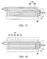
As shown in FIG. 1C, the packaging structure 140′ with other packaging structure type is used in the present embodiment. For instance, the packaging structure 140′ can comprise a plurality of package thin films. The package thin films include a plurality of organic package thin films 148 a and a plurality of inorganic package thin films 148 b. The organic thin films 148 a and the inorganic thin films 148 b are stacked on one another to provide a relatively better moisture-proof ability.
As shown in FIG. 1D, the packaging structure 140″ with other packaging structure type is used in the present embodiment. For instance, the packaging structure 140″ can comprise a sealant 142, an adhesion layer 144, a flexible cover 146, at least one layer of organic package thin films 148 a and at least one layer of inorganic package thin films 148 b. The organic thin films 148 a and the inorganic thin films 148 b are stacked on one another to provide a relatively better moisture-proof ability. The sealant 142 is disposed on the flexible substrate 110 to encircle the environmental sensitive element 120 and the flexible sacrificial layer 130. The adhesion layer 144 is disposed within the sealant 142 to cover the organic package thin films 148 a, the inorganic package thin films 148 b and the flexible sacrificial layer 130. Further, the flexible cover 146 is connected with the sealant 142 and the adhesion layer 144.
It should be noticed that the aforementioned organic package thin films 148 a and the inorganic package thin film 148 b can be arranged alone or alternately stacked on one another.
In a present embodiment, the material of the top electrode layer T can be, for example, as same as the material of the flexible protecting thin film 134, and the material of the sacrificial thin film 132 can be, for example, as same as the material of the hole transporting layer HTL. Therefore, the process for forming the flexible sacrificial layer 130 can be integrated with the process for forming the environmental sensitive element 120. In other words, the flexible sacrificial layer 130 and the environmental sensitive element 120 can be manufactured in the same process chamber without further modifying the current process procedure.
Second Embodiment
FIG. 2A and FIG. 2B are the cross-sectional views of a package of an environmental sensitive element according to the second embodiment of the present disclosure. As shown in FIG. 2A and FIG. 2B, the package 100 a of the environmental sensitive element of the present embodiment is similar to the package 100 of the environmental sensitive element of the first embodiment. More clearly, the thin film structure of the flexible sacrificial layer 130 a in the package 100 a is different from that of the flexible sacrificial layer 130 in the package 100. The flexible sacrificial layer 130 a comprises a plurality of sacrificial thin films 132 and a plurality of flexible protecting thin films 134, wherein the sacrificial thin films 132 and the flexible protecting thin films 134 are alternately stacked on one another and are configured on the top electrode layer T of the environmental sensitive element 120 and the bottommost sacrificial thin film 132 is connected to the top electrode layer T. Moreover, the flexible protecting thin films 134 of the present embodiment are disconnected to the top electrode layer T.
The Third Embodiment
FIG. 3A and FIG. 3B are the cross-sectional views of a package of an environmental sensitive element according to the third embodiment of the present disclosure. As shown in FIG. 3A and FIG. 3B, the package 100 b of the environmental sensitive element of the present embodiment is similar to the package 100 a of the environmental sensitive element of the second embodiment. More clearly, the thin film structure of the flexible sacrificial layer 130 b in the package 100 b is different from that of the flexible sacrificial layer 130 a in the package 100 a. The flexible sacrificial layer 130 b comprises a plurality of sacrificial thin films 132 and a plurality of flexible protecting thin films 134, wherein the sacrificial thin films 132 and the flexible protecting thin films 134 are alternately stacked on one another and are configured on the top electrode layer T of the environmental sensitive element 120 and the bottommost sacrificial thin film 132 and all of the flexible protecting thin films 134 are connected to the top electrode layer T.
Experimental Example
Table 1 is a detailed explanation of the structure of the package of the environmental sensitive element, wherein illuminant area of the package is about 0.3 centimeter×0.3 centimeter.
TABLE 1
Flexible
Lower EML EIL/top Structure Upper
Sustrate Electrode HTL (Dopant:Host) ETL electrode Layer Substrate
Experimental PES ITO NPB Ir(ppy)3 CBP Bphen LiF5 {acute over (Å)}/ NPB/Al Metal
group I 200 {acute over (Å)} 7% 300 {acute over (Å)} 300 {acute over (Å)} Al 1500 {acute over (Å)} 1500 {acute over (Å)}/ Foil
1500 {acute over (Å)}
Control group I PES ITO NPB Ir(ppy)3 CBP Bphen LiF5 {acute over (Å)}/ NPB/Al/ Metal
200 {acute over (Å)} 7% 300 {acute over (Å)} 300 {acute over (Å)} Al 1500 {acute over (Å)} 0 {acute over (Å)}/0 {acute over (Å)} Foil
The package of the environmental sensitive element manufactured according to the standards of the experimental group I and control group I is normally lighting on before it goes through the bending test. After the bending test (the package is bent for 500 times with a radius of curvature of about 5 centimeter), the package of the environmental sensitive element of the control group I can not light on. The package of the environmental sensitive element of the experimental group I is driven by a voltage of 4V to light on with a brightness about 820Cd/m^2 and a light emitting efficiency about 14.0 Cd/A before it goes through the bending test. After the bending test (the package is bent for 500 times with a radius of curvature of about 5 centimeter), the package of the environmental sensitive element of the experimental group I is driven by a voltage of 4V to light on with a brightness about 793 Cd/m^2 and a light emitting efficiency about 13.9 Cd/A. Obviously, the light emitting efficiency of the package of the environmental sensitive element of the experimental group I (i.e. one of the embodiments of the present disclosure) does not significantly decayed.
The Fourth Embodiment
FIG. 4A is the cross-sectional view of a package of an environmental sensitive element according to the fourth embodiment of the present disclosure. FIG. 4B is the top view of the package of the environmental sensitive element in FIG. 4A. As shown in FIG. 4A and FIG. 4B, the package 100 c of the environmental sensitive element of the present embodiment is similar to the package 100 of the environmental sensitive element of the first embodiment. Specifically, the first packaging structure 140′ covers the environmental sensitive element 120 and a first flexible sacrificial layer 150 is disposed on the first packaging structure 140′, wherein the environmental sensitive element 120 and the first flexible sacrificial layer 150 are located on two opposite sides of the first packaging structure 140′. The first packaging structure 140′ comprises at least one layer of organic package thin films 148 a and at least one layer of inorganic package thin films 148 b.
As shown in FIG. 4A, the first flexible sacrificial layer 150 comprises a first sacrificial thin film 152 and a first flexible protecting thin film 154, wherein the first sacrificial thin film 152 is configured on the first packaging structure 140′ and the first flexible protecting thin film 154 is configured on the first sacrificial thin film 152. It should be noticed that, the first sacrificial thin film 152 of the present embodiment is connected to the first packaging structure 140′, but the first flexible protecting thin film 154 is disconnected to the first packaging structure 140′. In other embodiments of the present disclosure, the first flexible protecting thin film 154 disposed on the first sacrificial thin film 152 can be connected to the first packaging structure 140′. The bonding strength between the first sacrificial thin film 152 and the first packaging structure 140′ is substantially equal to or lower than the bonding strength between two adjacent first thin films (DM, B and T) so that the delaminating phenomenon hardly happens between the adjacent first thin films (DM, B and T) but easily happens on the interface between the first sacrificial thin film 152 and the first packaging structure 140′ and on the interface between the first sacrificial thin film 152 and the first flexible protecting thin film 154 when the package of the environmental sensitive element is bent. Therefore, the first sacrificial thin film 152 and the first flexible protecting thin film 154 can effectively protect the first thin films (DM, B and T) from having delaminating phenomenon during the package is bent. In addition, the first flexible sacrificial layer 150 further has a UV cutting function so as to increase the life time of the environmental sensitive element 120. And also the first flexible sacrificial layer 150 further has a light out coupling function so as to increase the light efficiency of the environmental sensitive element 120.
In the present embodiment, the material of the first sacrificial thin film 152 is identical to the material of the sacrificial thin film 132, and the material of the first flexible protecting thin film 154 is identical to the material of the flexible protecting thin film 134. It should be noticed that the materials of the first sacrificial thin film 152 and the first flexible protecting thin film 154 in the first flexible sacrificial layer 150 are selected from different material groups such that the bonding strength between the first sacrificial thin film 152 and the first flexible protecting thin film 154 is substantially equal to or smaller than the bonding strength between the adjacent first thin films (DM, B and T).
As shown in FIG. 4A and FIG. 4B, the first flexible sacrificial layer 150 is greater than the size of the environmental sensitive element 120 in the present embodiment. However, in other embodiments, the size of the first flexible sacrificial layer 150 can be equal to the size of the environmental sensitive element 120.
The Fifth Embodiment
FIG. 5A is the cross-sectional view of a package of an environmental sensitive element according to the fifth embodiment of the present disclosure. FIG. 5B is the top view of the package of the environmental sensitive element in FIG. 5A. As shown in FIG. 5A and FIG. 5B, the package 100 d of the environmental sensitive element of the present embodiment is similar to the package 100 c of the environmental sensitive element of the fourth embodiment. Specifically, the package 100 d of the environmental sensitive element of the present embodiment further comprises a second packaging structure 160 covering the environmental sensitive element 120, the first packaging structure 140′ and the first flexible sacrificial layer 150. The second packaging structure 160 comprises a sealant 162, an adhesion layer 164 and a flexible cover 166. The sealant 162 is disposed on the flexible substrate 110 to encircle the environmental sensitive element 120 and the first flexible sacrificial layer 150. The adhesion layer 164 is disposed within the sealant 162 to cover the environmental sensitive element 120 and the first flexible sacrificial layer 150. Further, the flexible cover 166 is connected with the sealant 162 and the adhesion layer 164.
As shown in FIG. 5A and FIG. 5B, the sealant 162 of the second packaging structure 160 has a continuous pattern encircling the environmental sensitive element 120. However, in other embodiments, the sealant 162 of the second packaging structure 160 may have a non-continuous pattern encircling the environmental sensitive element 120. For example, the sealant 162 may includes a plurality of patterns separated from each other, wherein the separated patterns are arranged in a continuous form so as to encircle the environmental sensitive element 120. In addition, the material of the sealant 162 and the material of the adhesion layer 164 are different in the present embodiment. However, in other embodiments, the material of the sealant 162 and the material of the adhesion layer 164 may be identical.
The Sixth Embodiment
FIG. 6A is the cross-sectional view of a package of an environmental sensitive element according to the sixth embodiment of the present disclosure. FIG. 6B is the top view of the package of the environmental sensitive element in FIG. 6A. As shown in FIG. 6A and FIG. 6B, the package 100 e of the environmental sensitive element of the present embodiment is similar to the package 100 d of the environmental sensitive element of the fifth embodiment. Specifically, the adhesion layer 164 of a second packaging structure 160′ is a film type adhesive. The adhesion layer 164 covers the environmental sensitive element 120 and the first flexible sacrificial layer 150. Further, the flexible cover 166 is connected with the adhesion layer 164.
The Seventh Embodiment
FIG. 7 is the cross-sectional view of a package of an environmental sensitive element according to the seventh embodiment of the present disclosure. As shown in FIG. 7, the package 100 f of the environmental sensitive element of the present embodiment is similar to the package 100 c of the environmental sensitive element of the fourth embodiment. Specifically, the thin film structure of the first flexible sacrificial layer 150 a in the package 100 f is different from that of the first flexible sacrificial layer 150 in the package 100 c. The first flexible sacrificial layer 150 a comprises a plurality of first sacrificial thin films 152 and a plurality of first flexible protecting thin films 154, wherein the first sacrificial thin films 152 and the first flexible protecting thin films 154 are alternately stacked on one another and are configured on the first packaging structure 140′ and the bottommost first sacrificial thin film 152 is connected to the first packaging structure 140′. Moreover, as shown in FIG. 7, the first flexible protecting thin films 154 of the present embodiment are disconnected to the first packaging structure 140′.
The Eighth Embodiment
FIG. 8 is the cross-sectional view of a package of an environmental sensitive element according to the eighth embodiment of the present disclosure. As shown in FIG. 8, the package 100 g of the environmental sensitive element of the present embodiment is similar to the package 100 f of the environmental sensitive element in FIG. 7. Specifically, the thin film structure of the first flexible sacrificial layer 150 b in the package 100 g is different from that of the first flexible sacrificial layer 150 a in the package 100 f. The first flexible sacrificial layer 150 b comprises a plurality of first sacrificial thin films 152 and a plurality of first flexible protecting thin films 154, wherein the first sacrificial thin films 152 and the first flexible protecting thin films 154 are alternately stacked on one another and are configured on the first packaging structure 140′ and the bottommost first sacrificial thin film 152 and the bottommost first flexible protecting thin films 154 are connected to the first packaging structure 140′.
The Ninth Embodiment
FIG. 9 is the cross-sectional view of a package of an environmental sensitive element according to the ninth embodiment of the present disclosure. As shown in FIG. 9, the package 100 h of the environmental sensitive element of the present embodiment is similar to the package 100 c of the environmental sensitive element of the fourth embodiment. Specifically, the package 100 h further comprises a second flexible sacrificial layer 160 disposed on the environmental sensitive element 120.
As shown in FIG. 9, the second flexible sacrificial layer 170 comprises a second sacrificial thin film 172 and a second flexible protecting thin film 174, wherein the second sacrificial thin film 172 is configure on the top electrode layer T of the environmental sensitive element 120 and the second flexible protecting thin film 174 is configured on the second sacrificial thin film 172. It should be noticed that, the second sacrificial thin film 172 of the present embodiment is connected to the top electrode layer T, but the second flexible protecting thin film 174 is disconnected to the top electrode layer T. However, in other embodiments of the present disclosure, the second flexible protecting thin film 174 disposed on the second sacrificial thin film 172 can be connected to the top electrode layer T.
In the present embodiment, the material of the second sacrificial thin film 172 is identical to the material of the sacrificial thin film 132, and the material of the second flexible protecting thin film 174 is identical to the material of the flexible protecting thin film 134. It should be noticed that the materials of the second sacrificial thin film 172 and the second flexible protecting thin film 174 in the second flexible sacrificial layer 170 are selected from different material groups such that the bonding strength between the second sacrificial thin film 172 and the second flexible protecting thin film 174 is substantially equal to or smaller than the bonding strength between the adjacent first thin films (DM, B and T).
Further, the bonding strength between the second sacrificial thin film 172 and the top electrode layer T is substantially equal to or lower than the bonding strength between two adjacent first thin films (DM, B and T) so that the delaminating phenomenon hardly happens between the adjacent first thin films (DM, B and T) but easily happens on the interface between the second sacrificial thin film 172 and the top electrode layer T and on the interface between the second sacrificial thin film 172 and the second flexible protecting thin film 174 when the package of the environmental sensitive element is bent. Therefore, the second sacrificial thin film 172 and the second flexible protecting thin film 174 can effectively protect the first thin films (DM, B and T) from having delaminating phenomenon during the package is bent. In addition, the second flexible sacrificial layer 170 further has a UV cutting function so as to increase the life time of the environmental sensitive element 120. And also the second flexible sacrificial layer 170 further has a light out coupling function so as to increase the light efficiency of the environmental sensitive element 120.
The Tenth Embodiment
FIG. 10 is the cross-sectional view of a package of an environmental sensitive element according to the tenth embodiment of the present disclosure. As shown in FIG. 10, the package 100 i of the environmental sensitive element of the present embodiment is similar to the package 100 h of the environmental sensitive element of the ninth embodiment. Specifically, the package 100 i of the environmental sensitive element of the present embodiment further comprises a second packaging structure 160 covering the environmental sensitive element 120, the first packaging structure 140′, the first flexible sacrificial layer 150 and the second flexible sacrificial layer 170.
The Eleventh Embodiment
FIG. 11 is the cross-sectional view of a package of an environmental sensitive element according to the eleventh embodiment of the present disclosure. As shown in FIG. 11, the package 100 j of the environmental sensitive element of the present embodiment is similar to the package 100 h of the environmental sensitive element of the ninth embodiment. Specifically, the thin film structure of the first flexible sacrificial layer 150 a in the package 100 j is different from that of the first flexible sacrificial layer 150 in the package 100 h. The first flexible sacrificial layer 150 a comprises a plurality of first sacrificial thin films 152 and a plurality of first flexible protecting thin films 154, wherein the first sacrificial thin films 152 and the first flexible protecting thin films 154 are alternately stacked on one another and are configured on the first packaging structure 140′ and the bottommost first sacrificial thin film 152 is connected to the first packaging structure 140′. Moreover, as shown in FIG. 10, the first flexible protecting thin films 154 of the present embodiment are disconnected to the first packaging structure 140′.
Furthermore, the thin film structure of the second flexible sacrificial layer 170 a in the package 100 j is different from that of the second flexible sacrificial layer 170 in the package 100 h. The second flexible sacrificial layer 170 a comprises a plurality of second sacrificial thin films 172 and a plurality of second flexible protecting thin films 174, wherein the second sacrificial thin films 172 and the second flexible protecting thin films 174 are alternately stacked on one another and are configured on the environmental sensitive element 120, and the bottommost second sacrificial thin film 172 is connected to the environmental sensitive element 120. Moreover, as shown in FIG. 10, the second flexible protecting thin films 174 of the present embodiment are disconnected to the environmental sensitive element 120.
The Twelfth Embodiment
FIG. 12 is the cross-sectional view of a package of an environmental sensitive element according to the twelfth embodiment of the present disclosure. As shown in FIG. 12, the package 100 k of the environmental sensitive element of the present embodiment is similar to the package 100 j of the environmental sensitive element of the eleventh embodiment. Specifically, the thin film structures of the first flexible sacrificial layer 150 b in the package 100 k is different from that of the first flexible sacrificial layer 150 a in the package 100 j. The bottommost first sacrificial thin film 152 and the bottommost first flexible protecting thin film 154 are connected to the first packaging structure 140′.
Furthermore, the thin film structure of the second flexible sacrificial layer 170 b in the package 100 k is different from that of the second flexible sacrificial layer 170 a in the package 100 j. The bottommost second sacrificial thin film 172 and the bottommost second flexible protecting thin film 174 are connected to the environmental sensitive element 120.
According to the above embodiments and the experimental example, since the flexible sacrificial layer with various types is formed on the environmental sensitive element, when the environmental sensitive element is exaggeratedly bent, the delaminating happens in the flexible sacrificial layer. Therefore, the environmental sensitive element can be prevented from the delaminating phenomenon due to being bent and the structure of the environmental sensitive element can be prevented from being damaged during it is bent.

Claims (22)

What is claimed is:
1. A package of an environmental sensitive element, comprising:
a flexible substrate;
an environmental sensitive element disposed on the flexible substrate;
a first packaging structure covering the environmental sensitive element; and
a first flexible sacrificial layer disposed on the first packaging structure, and the first flexible sacrificial layer and the environmental sensitive element being located on two opposite sides of the first packaging structure, wherein the environmental sensitive element comprises a plurality of first thin films, the first flexible sacrificial layer includes a plurality of second thin films, and the bonding strength between two adjacent second thin films is equal to or lower than the bonding strength between two adjacent first thin films.
2. The package of claim 1, wherein the first thin films in the environmental sensitive element comprises:
a bottom electrode layer disposed on the flexible substrate;
a displaying medium disposed on bottom electrode layer; and
a top electrode layer disposed on the displaying medium.
3. The package of claim 2, wherein the second thin films in the first flexible sacrificial layer comprises:
at least one first sacrificial thin film disposed on the first packaging structure; and
at least one first flexible protecting thin film disposed on the first sacrificial thin film.
4. The package of claim 3, wherein the first sacrificial thin film is connected to the first packaging structure, and the first flexible protecting thin film is disconnected to the first packaging structure.
5. The package of claim 3, wherein both of the first sacrificial thin film and the first flexible protecting thin film are connected to the first packaging structure.
6. The package of claim 3, wherein the bonding strength between the first sacrificial thin film and the first packaging structure is equal to or lower than the bonding strength between two adjacent first thin films.
7. The package of claim 3, wherein the material of the first sacrificial thin film includes organic small molecular material with the molecular weight about 10 g/mol˜5000 g/mol.
8. The package of claim 3, wherein the material of the first sacrificial thin film includes organic oligomers with the molecular weight about 500 g/mol˜9000 g/mol.
9. The package of claim 3, wherein the material of the first sacrificial thin film includes organic small molecular material or a mixture of oligomers and inorganic material, and the atomic weight or the molecular weight of the inorganic material is about 3 g/mol˜500 g/mol.
10. The package of claim 3, wherein the material of the first sacrificial thin film includes Alq3 (Tris-(8-hydroxyquinoline)aluminum), alpha-NPB (N,N′-Dis(naphthalene-1-yl)-N,N′-diphenyl-benzidine), CuPc (Phalocyanine copper complex).
11. The package of claim 3, wherein the material of the first flexible protecting thin film comprises indium tin oxide (ITO), indium zinc oxide (IZO), aluminum doped zinc oxide (AZO), WO3, MoO3, SiOx, SiNX, SiOxNy, Al2O3, Al, Ag, Mg—Ag or Mg—Al.
12. The package of claim 3, wherein the material of the top electrode layer is equal to the material of the first flexible protecting thin film.
13. The package of claim 3, further comprising a second flexible sacrificial layer disposed on the environmental sensitive element, and the first packaging structure covering the environmental sensitive element and the second flexible sacrificial layer, wherein the second flexible sacrificial layer comprises a plurality of third thin films, and the bonding strength between two adjacent third thin films is equal to or lower than the bonding strength between two adjacent first thin films.
14. The package of claim 13, wherein the third thin films in the second flexible sacrificial layer comprises:
a second sacrificial thin film disposed on the top electrode; and
a second flexible protecting thin film disposed on the second sacrificial thin film.
15. The package of claim 13, wherein the third thin films in the second flexible sacrificial layer comprises:
a plurality of second sacrificial thin films; and
a plurality of second flexible protecting thin films, wherein the second sacrificial thin films and the second flexible protecting thin films are alternately stacked on the environmental sensitive element, and the bottommost second sacrificial thin film is connected to the top electrode layer.
16. The package of claim 1, wherein the material of the flexible substrate comprises plastic material or metal thin film.
17. The package of claim 1, wherein the first packaging structure comprises a plurality of package thin films stacked by one another.
18. The package of claim 17, wherein the package thin films comprises at least a layer of organic package thin film or a least a layer of inorganic package thin film.
19. The package of claim 17, wherein the package thin films comprise:
a plurality of organic package thin films; and
a plurality of inorganic package thin films, wherein the organic package thin films and the inorganic package thin films are alternately stacked on one another.
20. The package of claim 1, further comprising a second packaging structure, wherein the second packaging structure comprises:
a sealant disposed on the flexible substrate to encircle the environmental sensitive element, the first packaging structure and the first flexible sacrificial layer;
an adhesion layer disposed within the sealant to cover the environmental sensitive element, the first packaging structure and the first flexible sacrificial layer; and
a flexible cover connected with the sealant and the adhesion layer.
21. The package of claim 1, further comprising a second packaging structure, wherein the second packaging structure comprises:
an adhesion layer covering the environmental sensitive element, the first packaging structure and the first flexible sacrificial layer; and
a flexible cover connected with the sealant and the adhesion layer.
22. The package of claim 1, wherein the material of the first flexible sacrificial layer includes UV cutting material.
US13/867,136 2009-09-15 2013-04-22 Package of environmental sensitive element Active 2030-09-12 US9101005B2 (en)

Priority Applications (3)

Application Number Priority Date Filing Date Title
US13/867,136 US9101005B2 (en) 2009-09-15 2013-04-22 Package of environmental sensitive element
US14/730,253 US9224700B2 (en) 2009-09-15 2015-06-04 Package of environmental sensitive element
US14/948,394 US9660218B2 (en) 2009-09-15 2015-11-23 Package of environmental sensitive element

Applications Claiming Priority (5)

Application Number Priority Date Filing Date Title
TW98131092 2009-09-15
TW098131092A TWI407535B (en) 2009-09-15 2009-09-15 Package of environmental sensitive element
TW98131092A 2009-09-15
US12/703,155 US8446730B2 (en) 2009-09-15 2010-02-09 Package of environmental sensitive element
US13/867,136 US9101005B2 (en) 2009-09-15 2013-04-22 Package of environmental sensitive element

Related Parent Applications (1)

Application Number Title Priority Date Filing Date
US12/703,155 Continuation-In-Part US8446730B2 (en) 2009-09-15 2010-02-09 Package of environmental sensitive element

Related Child Applications (1)

Application Number Title Priority Date Filing Date
US14/730,253 Division US9224700B2 (en) 2009-09-15 2015-06-04 Package of environmental sensitive element

Publications (2)

Publication Number Publication Date
US20130229108A1 US20130229108A1 (en) 2013-09-05
US9101005B2 true US9101005B2 (en) 2015-08-04

Family

ID=49042444

Family Applications (2)

Application Number Title Priority Date Filing Date
US13/867,136 Active 2030-09-12 US9101005B2 (en) 2009-09-15 2013-04-22 Package of environmental sensitive element
US14/730,253 Active US9224700B2 (en) 2009-09-15 2015-06-04 Package of environmental sensitive element

Family Applications After (1)

Application Number Title Priority Date Filing Date
US14/730,253 Active US9224700B2 (en) 2009-09-15 2015-06-04 Package of environmental sensitive element

Country Status (1)

Country Link
US (2) US9101005B2 (en)

Cited By (1)

* Cited by examiner, † Cited by third party
Publication number Priority date Publication date Assignee Title
WO2020238947A1 (en) * 2019-05-31 2020-12-03 京东方科技集团股份有限公司 Encapsulation cover plate and preparation method of the encapsulation cover plate, display panel and preparation method thereof

Families Citing this family (10)

* Cited by examiner, † Cited by third party
Publication number Priority date Publication date Assignee Title
CN105493627A (en) * 2013-08-28 2016-04-13 夏普株式会社 Electroluminescent device and method for manufacturing same
KR102203446B1 (en) * 2014-05-28 2021-01-18 엘지디스플레이 주식회사 Organic light emitting display device and manufacturing method of the same
JP2016072127A (en) * 2014-09-30 2016-05-09 ソニー株式会社 Organic el display device and manufacturing method of the same and electronic apparatus
US9276236B1 (en) * 2015-02-08 2016-03-01 Shenzhen China Star Optoelectronics Technology Co., Ltd OLED element
CN106783757A (en) * 2015-11-23 2017-05-31 财团法人工业技术研究院 Environment sensitive component encapsulation
CN106684259B (en) * 2017-01-18 2018-08-14 深圳市华星光电技术有限公司 OLED encapsulation method and OLED encapsulating structures
CN108428804A (en) * 2018-04-19 2018-08-21 武汉华星光电技术有限公司 Oled display panel and its packaging method
CN108470854A (en) * 2018-04-25 2018-08-31 深圳市华星光电技术有限公司 WOLED display panels and preparation method thereof
CN109037482A (en) * 2018-08-03 2018-12-18 武汉华星光电半导体显示技术有限公司 The preparation method and OLED display of thin-film encapsulation layer
CN110190032B (en) * 2019-05-16 2020-07-03 昆山国显光电有限公司 Display panel and display device

Citations (28)

* Cited by examiner, † Cited by third party
Publication number Priority date Publication date Assignee Title
US5686360A (en) * 1995-11-30 1997-11-11 Motorola Passivation of organic devices
US5855994A (en) 1996-07-10 1999-01-05 International Business Machines Corporation Siloxane and siloxane derivatives as encapsulants for organic light emitting devices
US20030032210A1 (en) * 2001-07-16 2003-02-13 Semiconductor Energy Laboratory Co., Ltd. Semiconductor device and peeling off method and method of manufacturing semiconductor device
US20030034497A1 (en) * 2001-06-20 2003-02-20 Semiconductor Energy Laboratory Co., Ltd. Light emitting device and method of manufacturing the same
US20030042562A1 (en) 2001-08-30 2003-03-06 Carsten Giebeler Magnetoresistive device and electronic device
US20030048074A1 (en) 2001-09-12 2003-03-13 Jui-Ming Ni Method for packaging organic electroluminescent components with polymer passivation layer and structure thereof
US20030098647A1 (en) * 2001-11-27 2003-05-29 Silvernail Jeffrey Alan Protected organic optoelectronic devices
US20030127973A1 (en) * 2002-01-10 2003-07-10 Weaver Michael Stuart OLEDs having increased external electroluminescence quantum efficiencies
US6624568B2 (en) 2001-03-28 2003-09-23 Universal Display Corporation Multilayer barrier region containing moisture- and oxygen-absorbing material for optoelectronic devices
US20040069985A1 (en) * 2002-10-15 2004-04-15 Eastman Kodak Company Oled display with circular polarizer
US20040189196A1 (en) * 2002-10-15 2004-09-30 Eastman Kodak Company OLED display with circular polarizer
US20040197944A1 (en) 2003-04-04 2004-10-07 Toppoly Optoelectronics Corp. Method of forming encapsulation structure for organic light-emitting device
US20050179379A1 (en) 2004-02-17 2005-08-18 Han-Ki Kim Organic light-emitting device having thin-film encapsulation portion, method of manufacturing the device, and apparatus for forming a film
US20050285520A1 (en) 2004-06-24 2005-12-29 Eastman Kodak Company OLED display having thermally conductive adhesive
US20050285519A1 (en) 2004-06-24 2005-12-29 Eastman Kodak Company OLED display having thermally conductive material
US20060006798A1 (en) 2002-09-30 2006-01-12 Microemissive Displays Limited Passivation layer
US20060269782A1 (en) 2005-05-25 2006-11-30 Eastman Kodak Company OLED electron-transporting layer
US20070049155A1 (en) 2005-08-25 2007-03-01 Vitex Systems, Inc. Encapsulated devices and method of making
US20070241674A1 (en) 2006-04-13 2007-10-18 Au Optronics Corp. Organic electroluminescent display oled and fabrication method thereof
US20080012477A1 (en) 2006-07-12 2008-01-17 Samsung Electronics Co., Ltd. Organic light emitting diode display and method for manufacturing thereof
US20080259576A1 (en) 2005-10-13 2008-10-23 Nxp B.V. Electronic Device or Circuit and Method for Fabricating the Same
US20080303435A1 (en) * 2007-06-11 2008-12-11 Cok Ronald S Led device having improved contrast
US20090072734A1 (en) 2005-03-30 2009-03-19 Pioneer Corporation Organic el display device, method of manufacturing organic el display device, organic transistor, and method of manufacturing organic transistor
US20090278449A1 (en) * 2008-05-06 2009-11-12 Nack Bong Choi Flexible organic electro-luminescence display device and manufacturing method thereof
US20110063808A1 (en) 2009-09-15 2011-03-17 Industrial Technology Research Institute Package of environmental sensitive element
US20120024722A1 (en) 2010-07-29 2012-02-02 Industrial Technology Research Institute Package of environmental sensitive element and encapsulation method of the same
US20120064278A1 (en) 2010-09-10 2012-03-15 Industrial Technology Research Institute Package of environmental sensitive element and encapsulation method thereof
US8366505B2 (en) * 2008-12-30 2013-02-05 Industrial Technology Research Institute Apparatus of organic light emitting diode and packaging method of the same

Family Cites Families (8)

* Cited by examiner, † Cited by third party
Publication number Priority date Publication date Assignee Title
GB2399088B (en) * 2001-11-30 2005-07-13 Sumitomo Chemical Co Electroluminescent element
JPWO2007034647A1 (en) * 2005-09-20 2009-03-19 コニカミノルタホールディングス株式会社 Method for manufacturing organic electroluminescence element, organic electroluminescence display device
JP4702009B2 (en) * 2005-11-22 2011-06-15 セイコーエプソン株式会社 LIGHT EMITTING DEVICE AND ELECTRONIC DEVICE
JP4600254B2 (en) * 2005-11-22 2010-12-15 セイコーエプソン株式会社 LIGHT EMITTING DEVICE AND ELECTRONIC DEVICE
JP5090197B2 (en) * 2007-02-20 2012-12-05 富士フイルム株式会社 LAMINATE MANUFACTURING METHOD, BARRIER FILM SUBSTRATE, DEVICE, AND OPTICAL MEMBER
JP5198131B2 (en) * 2007-05-14 2013-05-15 富士フイルム株式会社 Barrier film and element
JP5140376B2 (en) * 2007-10-16 2013-02-06 富士フイルム株式会社 Gas barrier film and environmentally sensitive device
US8358066B1 (en) * 2011-08-10 2013-01-22 General Electric Company Organic light emitting diode package with energy blocking layer

Patent Citations (33)

* Cited by examiner, † Cited by third party
Publication number Priority date Publication date Assignee Title
US5757126A (en) * 1995-11-30 1998-05-26 Motorola, Inc. Passivated organic device having alternating layers of polymer and dielectric
US5686360A (en) * 1995-11-30 1997-11-11 Motorola Passivation of organic devices
US5855994A (en) 1996-07-10 1999-01-05 International Business Machines Corporation Siloxane and siloxane derivatives as encapsulants for organic light emitting devices
US6624568B2 (en) 2001-03-28 2003-09-23 Universal Display Corporation Multilayer barrier region containing moisture- and oxygen-absorbing material for optoelectronic devices
US20080303408A1 (en) * 2001-06-20 2008-12-11 Semiconductor Energy Laboratory Co., Ltd. Light emitting device and method of manufacturing the same
US20050127371A1 (en) * 2001-06-20 2005-06-16 Semiconductor Energy Laboratory Co., Ltd. Light emitting device and method of manufacturing the same
US20030034497A1 (en) * 2001-06-20 2003-02-20 Semiconductor Energy Laboratory Co., Ltd. Light emitting device and method of manufacturing the same
US20030032210A1 (en) * 2001-07-16 2003-02-13 Semiconductor Energy Laboratory Co., Ltd. Semiconductor device and peeling off method and method of manufacturing semiconductor device
US20030042562A1 (en) 2001-08-30 2003-03-06 Carsten Giebeler Magnetoresistive device and electronic device
US20050145909A1 (en) 2001-08-30 2005-07-07 Carsten Giebeler Magnetoresistive device and electronic device
US20030048074A1 (en) 2001-09-12 2003-03-13 Jui-Ming Ni Method for packaging organic electroluminescent components with polymer passivation layer and structure thereof
US20040150332A1 (en) 2001-09-12 2004-08-05 Windell Corporation Method for packaging organic electroluminescent components with polymer passivation layer and structure thereof
US20030098647A1 (en) * 2001-11-27 2003-05-29 Silvernail Jeffrey Alan Protected organic optoelectronic devices
US20030127973A1 (en) * 2002-01-10 2003-07-10 Weaver Michael Stuart OLEDs having increased external electroluminescence quantum efficiencies
US20060006798A1 (en) 2002-09-30 2006-01-12 Microemissive Displays Limited Passivation layer
US20040189196A1 (en) * 2002-10-15 2004-09-30 Eastman Kodak Company OLED display with circular polarizer
US20040069985A1 (en) * 2002-10-15 2004-04-15 Eastman Kodak Company Oled display with circular polarizer
US20040197944A1 (en) 2003-04-04 2004-10-07 Toppoly Optoelectronics Corp. Method of forming encapsulation structure for organic light-emitting device
US20050179379A1 (en) 2004-02-17 2005-08-18 Han-Ki Kim Organic light-emitting device having thin-film encapsulation portion, method of manufacturing the device, and apparatus for forming a film
US20050285519A1 (en) 2004-06-24 2005-12-29 Eastman Kodak Company OLED display having thermally conductive material
US20050285520A1 (en) 2004-06-24 2005-12-29 Eastman Kodak Company OLED display having thermally conductive adhesive
US20090072734A1 (en) 2005-03-30 2009-03-19 Pioneer Corporation Organic el display device, method of manufacturing organic el display device, organic transistor, and method of manufacturing organic transistor
US20060269782A1 (en) 2005-05-25 2006-11-30 Eastman Kodak Company OLED electron-transporting layer
US20070049155A1 (en) 2005-08-25 2007-03-01 Vitex Systems, Inc. Encapsulated devices and method of making
US20080259576A1 (en) 2005-10-13 2008-10-23 Nxp B.V. Electronic Device or Circuit and Method for Fabricating the Same
US20070241674A1 (en) 2006-04-13 2007-10-18 Au Optronics Corp. Organic electroluminescent display oled and fabrication method thereof
US20080012477A1 (en) 2006-07-12 2008-01-17 Samsung Electronics Co., Ltd. Organic light emitting diode display and method for manufacturing thereof
US20080303435A1 (en) * 2007-06-11 2008-12-11 Cok Ronald S Led device having improved contrast
US20090278449A1 (en) * 2008-05-06 2009-11-12 Nack Bong Choi Flexible organic electro-luminescence display device and manufacturing method thereof
US8366505B2 (en) * 2008-12-30 2013-02-05 Industrial Technology Research Institute Apparatus of organic light emitting diode and packaging method of the same
US20110063808A1 (en) 2009-09-15 2011-03-17 Industrial Technology Research Institute Package of environmental sensitive element
US20120024722A1 (en) 2010-07-29 2012-02-02 Industrial Technology Research Institute Package of environmental sensitive element and encapsulation method of the same
US20120064278A1 (en) 2010-09-10 2012-03-15 Industrial Technology Research Institute Package of environmental sensitive element and encapsulation method thereof

Cited By (1)

* Cited by examiner, † Cited by third party
Publication number Priority date Publication date Assignee Title
WO2020238947A1 (en) * 2019-05-31 2020-12-03 京东方科技集团股份有限公司 Encapsulation cover plate and preparation method of the encapsulation cover plate, display panel and preparation method thereof

Also Published As

Publication number Publication date
US20130229108A1 (en) 2013-09-05
US20150270231A1 (en) 2015-09-24
US9224700B2 (en) 2015-12-29

Similar Documents

Publication Publication Date Title
US9224700B2 (en) Package of environmental sensitive element
US8446730B2 (en) Package of environmental sensitive element
US9660218B2 (en) Package of environmental sensitive element
US7977877B2 (en) Flat panel OLED device having deformable substrate
US7259505B2 (en) OLED display with circular polarizer
EP1463117B1 (en) Oled display with photosensor
US6936964B2 (en) OLED lamp
US7038373B2 (en) Organic light emitting diode display
US6936961B2 (en) Cascaded organic electroluminescent device having connecting units with N-type and P-type organic layers
EP1351323A2 (en) Desiccant structures for oled displays
US20060006792A1 (en) Flat panel light emitting devices with two sided
US6818329B1 (en) Organic electroluminescent devices having a metal sub-layer within a hole-transporting region
TWI640803B (en) Functional polarizing film and organic light-emitting display apparatus including the same
JP5558836B2 (en) Flat panel OLED device with deformable substrate
WO2005078820A1 (en) Full-color organic display having improved blue emission
GB2390215A (en) OLED display with surface plasmon outcoupling
WO2005060016A2 (en) White-emitting microcavity oled device
WO2008140644A1 (en) Electroluminescent device having improved light output
JP2006278139A (en) Spontaneous light emitting panel and manufacturing method of the same
US20060132027A1 (en) Method and display element with reduced thermal stress
US20040069985A1 (en) Oled display with circular polarizer
US20050170551A1 (en) Manufacture of flat panel light emitting devices
WO2014041616A1 (en) Organic el device
CN106783757A (en) Environment sensitive component encapsulation
WO2014041615A1 (en) Organic el device

Legal Events

Date Code Title Description
AS Assignment

Owner name: INDUSTRIAL TECHNOLOGY RESEARCH INSTITUTE, TAIWAN

Free format text: ASSIGNMENT OF ASSIGNORS INTEREST;ASSIGNOR:CHEN, KUANG-JUNG;REEL/FRAME:030290/0711

Effective date: 20130419

STCF Information on status: patent grant

Free format text: PATENTED CASE

MAFP Maintenance fee payment

Free format text: PAYMENT OF MAINTENANCE FEE, 4TH YEAR, LARGE ENTITY (ORIGINAL EVENT CODE: M1551); ENTITY STATUS OF PATENT OWNER: LARGE ENTITY

Year of fee payment: 4

AS Assignment

Owner name: HANNSTAR DISPLAY CORPORATION, TAIWAN

Free format text: ASSIGNMENT OF ASSIGNORS INTEREST;ASSIGNOR:INDUSTRIAL TECHNOLOGY RESEARCH INSTITUTE;REEL/FRAME:059365/0305

Effective date: 20220124

MAFP Maintenance fee payment

Free format text: PAYMENT OF MAINTENANCE FEE, 8TH YEAR, LARGE ENTITY (ORIGINAL EVENT CODE: M1552); ENTITY STATUS OF PATENT OWNER: LARGE ENTITY

Year of fee payment: 8