US9105798B2 - Preparation of CIGS absorber layers using coated semiconductor nanoparticle and nanowire networks - Google Patents
Preparation of CIGS absorber layers using coated semiconductor nanoparticle and nanowire networks Download PDFInfo
- Publication number
- US9105798B2 US9105798B2 US13/893,756 US201313893756A US9105798B2 US 9105798 B2 US9105798 B2 US 9105798B2 US 201313893756 A US201313893756 A US 201313893756A US 9105798 B2 US9105798 B2 US 9105798B2
- Authority
- US
- United States
- Prior art keywords
- cigs
- solution
- ink
- nanoparticles
- precursor
- Prior art date
- Legal status (The legal status is an assumption and is not a legal conclusion. Google has not performed a legal analysis and makes no representation as to the accuracy of the status listed.)
- Active, expires
Links
- 239000002105 nanoparticle Substances 0.000 title claims abstract description 63
- 239000002070 nanowire Substances 0.000 title claims abstract description 46
- 239000006096 absorbing agent Substances 0.000 title claims abstract description 6
- 239000004065 semiconductor Substances 0.000 title abstract description 4
- 238000000034 method Methods 0.000 claims abstract description 66
- 239000002243 precursor Substances 0.000 claims abstract description 60
- 230000002776 aggregation Effects 0.000 claims abstract description 11
- 238000004220 aggregation Methods 0.000 claims abstract description 11
- 229910052733 gallium Inorganic materials 0.000 claims abstract description 11
- 150000003839 salts Chemical class 0.000 claims abstract description 10
- 239000002184 metal Substances 0.000 claims abstract description 8
- 229910052751 metal Inorganic materials 0.000 claims abstract description 8
- OKTJSMMVPCPJKN-UHFFFAOYSA-N Carbon Chemical compound [C] OKTJSMMVPCPJKN-UHFFFAOYSA-N 0.000 claims abstract description 6
- QTBSBXVTEAMEQO-UHFFFAOYSA-M Acetate Chemical compound CC([O-])=O QTBSBXVTEAMEQO-UHFFFAOYSA-M 0.000 claims abstract description 4
- 229910001510 metal chloride Inorganic materials 0.000 claims abstract description 4
- 239000000758 substrate Substances 0.000 claims description 30
- 238000004544 sputter deposition Methods 0.000 claims description 26
- 239000000843 powder Substances 0.000 claims description 23
- 238000005507 spraying Methods 0.000 claims description 19
- 239000011521 glass Substances 0.000 claims description 18
- 238000010438 heat treatment Methods 0.000 claims description 16
- 238000003756 stirring Methods 0.000 claims description 16
- 239000002904 solvent Substances 0.000 claims description 14
- 238000000224 chemical solution deposition Methods 0.000 claims description 13
- 230000002194 synthesizing effect Effects 0.000 claims description 13
- OKKJLVBELUTLKV-UHFFFAOYSA-N Methanol Chemical compound OC OKKJLVBELUTLKV-UHFFFAOYSA-N 0.000 claims description 12
- 238000001704 evaporation Methods 0.000 claims description 12
- 239000011669 selenium Substances 0.000 claims description 12
- 239000007921 spray Substances 0.000 claims description 12
- 239000000654 additive Substances 0.000 claims description 10
- 238000000151 deposition Methods 0.000 claims description 9
- 230000000694 effects Effects 0.000 claims description 9
- 239000002562 thickening agent Substances 0.000 claims description 9
- 239000000203 mixture Substances 0.000 claims description 8
- 230000008719 thickening Effects 0.000 claims description 8
- UMGDCJDMYOKAJW-UHFFFAOYSA-N thiourea Chemical compound NC(N)=S UMGDCJDMYOKAJW-UHFFFAOYSA-N 0.000 claims description 8
- 230000008859 change Effects 0.000 claims description 7
- 229910052802 copper Inorganic materials 0.000 claims description 7
- 238000001035 drying Methods 0.000 claims description 7
- 229910052738 indium Inorganic materials 0.000 claims description 7
- 239000002245 particle Substances 0.000 claims description 7
- 239000011858 nanopowder Substances 0.000 claims description 6
- XLYOFNOQVPJJNP-UHFFFAOYSA-N water Chemical compound O XLYOFNOQVPJJNP-UHFFFAOYSA-N 0.000 claims description 6
- 150000002500 ions Chemical class 0.000 claims description 5
- CSCPPACGZOOCGX-UHFFFAOYSA-N Acetone Chemical compound CC(C)=O CSCPPACGZOOCGX-UHFFFAOYSA-N 0.000 claims description 4
- LFQSCWFLJHTTHZ-UHFFFAOYSA-N Ethanol Chemical compound CCO LFQSCWFLJHTTHZ-UHFFFAOYSA-N 0.000 claims description 4
- 239000001856 Ethyl cellulose Substances 0.000 claims description 4
- ZZSNKZQZMQGXPY-UHFFFAOYSA-N Ethyl cellulose Chemical compound CCOCC1OC(OC)C(OCC)C(OCC)C1OC1C(O)C(O)C(OC)C(CO)O1 ZZSNKZQZMQGXPY-UHFFFAOYSA-N 0.000 claims description 4
- 229910003310 Ni-Al Inorganic materials 0.000 claims description 4
- XSQUKJJJFZCRTK-UHFFFAOYSA-N Urea Natural products NC(N)=O XSQUKJJJFZCRTK-UHFFFAOYSA-N 0.000 claims description 4
- 239000007822 coupling agent Substances 0.000 claims description 4
- 239000002270 dispersing agent Substances 0.000 claims description 4
- 229920001249 ethyl cellulose Polymers 0.000 claims description 4
- 235000019325 ethyl cellulose Nutrition 0.000 claims description 4
- 239000012456 homogeneous solution Substances 0.000 claims description 4
- PSCMQHVBLHHWTO-UHFFFAOYSA-K indium(iii) chloride Chemical compound Cl[In](Cl)Cl PSCMQHVBLHHWTO-UHFFFAOYSA-K 0.000 claims description 4
- 238000002156 mixing Methods 0.000 claims description 4
- 239000003960 organic solvent Substances 0.000 claims description 4
- 238000005303 weighing Methods 0.000 claims description 4
- BUGBHKTXTAQXES-UHFFFAOYSA-N Selenium Chemical compound [Se] BUGBHKTXTAQXES-UHFFFAOYSA-N 0.000 claims description 3
- 229910002804 graphite Inorganic materials 0.000 claims description 3
- 239000010439 graphite Substances 0.000 claims description 3
- FAXDZWQIWUSWJH-UHFFFAOYSA-N 3-methoxypropan-1-amine Chemical compound COCCCN FAXDZWQIWUSWJH-UHFFFAOYSA-N 0.000 claims description 2
- 229910005267 GaCl3 Inorganic materials 0.000 claims description 2
- 229910017906 NH3H2O Inorganic materials 0.000 claims description 2
- 229910052782 aluminium Inorganic materials 0.000 claims description 2
- 238000009835 boiling Methods 0.000 claims description 2
- QCUOBSQYDGUHHT-UHFFFAOYSA-L cadmium sulfate Chemical compound [Cd+2].[O-]S([O-])(=O)=O QCUOBSQYDGUHHT-UHFFFAOYSA-L 0.000 claims description 2
- 229910000369 cadmium(II) sulfate Inorganic materials 0.000 claims description 2
- 238000011010 flushing procedure Methods 0.000 claims description 2
- UPWPDUACHOATKO-UHFFFAOYSA-K gallium trichloride Chemical compound Cl[Ga](Cl)Cl UPWPDUACHOATKO-UHFFFAOYSA-K 0.000 claims description 2
- 238000011068 loading method Methods 0.000 claims description 2
- 229910052759 nickel Inorganic materials 0.000 claims description 2
- 239000006259 organic additive Substances 0.000 claims description 2
- 239000010453 quartz Substances 0.000 claims description 2
- VYPSYNLAJGMNEJ-UHFFFAOYSA-N silicon dioxide Inorganic materials O=[Si]=O VYPSYNLAJGMNEJ-UHFFFAOYSA-N 0.000 claims description 2
- 239000007787 solid Substances 0.000 claims description 2
- RBNWAMSGVWEHFP-UHFFFAOYSA-N trans-p-Menthane-1,8-diol Chemical compound CC(C)(O)C1CCC(C)(O)CC1 RBNWAMSGVWEHFP-UHFFFAOYSA-N 0.000 claims description 2
- 238000005406 washing Methods 0.000 claims description 2
- 238000001816 cooling Methods 0.000 claims 5
- MPTQRFCYZCXJFQ-UHFFFAOYSA-L copper(II) chloride dihydrate Chemical compound O.O.[Cl-].[Cl-].[Cu+2] MPTQRFCYZCXJFQ-UHFFFAOYSA-L 0.000 claims 1
- GCLGEJMYGQKIIW-UHFFFAOYSA-H sodium hexametaphosphate Chemical compound [Na]OP1(=O)OP(=O)(O[Na])OP(=O)(O[Na])OP(=O)(O[Na])OP(=O)(O[Na])OP(=O)(O[Na])O1 GCLGEJMYGQKIIW-UHFFFAOYSA-H 0.000 claims 1
- 235000019982 sodium hexametaphosphate Nutrition 0.000 claims 1
- 230000015572 biosynthetic process Effects 0.000 abstract description 8
- 239000011261 inert gas Substances 0.000 abstract description 5
- 239000003795 chemical substances by application Substances 0.000 abstract description 4
- 229910052799 carbon Inorganic materials 0.000 abstract description 3
- 238000004140 cleaning Methods 0.000 abstract description 3
- 230000008569 process Effects 0.000 description 22
- 239000010408 film Substances 0.000 description 19
- 239000000976 ink Substances 0.000 description 15
- 239000010949 copper Substances 0.000 description 7
- 238000010586 diagram Methods 0.000 description 7
- 238000004519 manufacturing process Methods 0.000 description 7
- 239000010409 thin film Substances 0.000 description 7
- 239000007789 gas Substances 0.000 description 6
- 238000006243 chemical reaction Methods 0.000 description 5
- 238000003786 synthesis reaction Methods 0.000 description 5
- ZWEHNKRNPOVVGH-UHFFFAOYSA-N 2-Butanone Chemical compound CCC(C)=O ZWEHNKRNPOVVGH-UHFFFAOYSA-N 0.000 description 4
- -1 gallium selenides Chemical class 0.000 description 4
- 239000000463 material Substances 0.000 description 4
- 230000008901 benefit Effects 0.000 description 3
- 239000011230 binding agent Substances 0.000 description 3
- 230000008021 deposition Effects 0.000 description 3
- 238000005516 engineering process Methods 0.000 description 3
- OAKJQQAXSVQMHS-UHFFFAOYSA-N Hydrazine Chemical compound NN OAKJQQAXSVQMHS-UHFFFAOYSA-N 0.000 description 2
- 239000012298 atmosphere Substances 0.000 description 2
- 230000004888 barrier function Effects 0.000 description 2
- 239000011258 core-shell material Substances 0.000 description 2
- 230000004048 modification Effects 0.000 description 2
- 238000012986 modification Methods 0.000 description 2
- 238000013341 scale-up Methods 0.000 description 2
- 231100000331 toxic Toxicity 0.000 description 2
- 230000002588 toxic effect Effects 0.000 description 2
- DKIDEFUBRARXTE-UHFFFAOYSA-N 3-mercaptopropanoic acid Chemical compound OC(=O)CCS DKIDEFUBRARXTE-UHFFFAOYSA-N 0.000 description 1
- 241001279686 Allium moly Species 0.000 description 1
- RYGMFSIKBFXOCR-UHFFFAOYSA-N Copper Chemical compound [Cu] RYGMFSIKBFXOCR-UHFFFAOYSA-N 0.000 description 1
- 229910021592 Copper(II) chloride Inorganic materials 0.000 description 1
- 240000005636 Dryobalanops aromatica Species 0.000 description 1
- UFHFLCQGNIYNRP-UHFFFAOYSA-N Hydrogen Chemical compound [H][H] UFHFLCQGNIYNRP-UHFFFAOYSA-N 0.000 description 1
- DGAQECJNVWCQMB-PUAWFVPOSA-M Ilexoside XXIX Chemical compound C[C@@H]1CC[C@@]2(CC[C@@]3(C(=CC[C@H]4[C@]3(CC[C@@H]5[C@@]4(CC[C@@H](C5(C)C)OS(=O)(=O)[O-])C)C)[C@@H]2[C@]1(C)O)C)C(=O)O[C@H]6[C@@H]([C@H]([C@@H]([C@H](O6)CO)O)O)O.[Na+] DGAQECJNVWCQMB-PUAWFVPOSA-M 0.000 description 1
- 238000010521 absorption reaction Methods 0.000 description 1
- 239000003963 antioxidant agent Substances 0.000 description 1
- 235000006708 antioxidants Nutrition 0.000 description 1
- 230000005540 biological transmission Effects 0.000 description 1
- 239000000919 ceramic Substances 0.000 description 1
- DVRDHUBQLOKMHZ-UHFFFAOYSA-N chalcopyrite Chemical compound [S-2].[S-2].[Fe+2].[Cu+2] DVRDHUBQLOKMHZ-UHFFFAOYSA-N 0.000 description 1
- 229910052951 chalcopyrite Inorganic materials 0.000 description 1
- 238000001311 chemical methods and process Methods 0.000 description 1
- 239000003153 chemical reaction reagent Substances 0.000 description 1
- 231100000481 chemical toxicant Toxicity 0.000 description 1
- 238000010549 co-Evaporation Methods 0.000 description 1
- 238000000576 coating method Methods 0.000 description 1
- 239000000084 colloidal system Substances 0.000 description 1
- 238000010276 construction Methods 0.000 description 1
- 229910021419 crystalline silicon Inorganic materials 0.000 description 1
- ZZEMEJKDTZOXOI-UHFFFAOYSA-N digallium;selenium(2-) Chemical compound [Ga+3].[Ga+3].[Se-2].[Se-2].[Se-2] ZZEMEJKDTZOXOI-UHFFFAOYSA-N 0.000 description 1
- 239000003995 emulsifying agent Substances 0.000 description 1
- 239000002360 explosive Substances 0.000 description 1
- XLYOFNOQVPJJNP-ZSJDYOACSA-N heavy water Substances [2H]O[2H] XLYOFNOQVPJJNP-ZSJDYOACSA-N 0.000 description 1
- 229910052739 hydrogen Inorganic materials 0.000 description 1
- 239000001257 hydrogen Substances 0.000 description 1
- APFVFJFRJDLVQX-UHFFFAOYSA-N indium atom Chemical compound [In] APFVFJFRJDLVQX-UHFFFAOYSA-N 0.000 description 1
- AKUCEXGLFUSJCD-UHFFFAOYSA-N indium(3+);selenium(2-) Chemical compound [Se-2].[Se-2].[Se-2].[In+3].[In+3] AKUCEXGLFUSJCD-UHFFFAOYSA-N 0.000 description 1
- 239000004615 ingredient Substances 0.000 description 1
- 230000031700 light absorption Effects 0.000 description 1
- 239000007791 liquid phase Substances 0.000 description 1
- 229910003455 mixed metal oxide Inorganic materials 0.000 description 1
- 239000003973 paint Substances 0.000 description 1
- 239000004014 plasticizer Substances 0.000 description 1
- 239000003755 preservative agent Substances 0.000 description 1
- 238000007639 printing Methods 0.000 description 1
- 230000035484 reaction time Effects 0.000 description 1
- 230000009467 reduction Effects 0.000 description 1
- 238000011946 reduction process Methods 0.000 description 1
- SPVXKVOXSXTJOY-UHFFFAOYSA-N selane Chemical compound [SeH2] SPVXKVOXSXTJOY-UHFFFAOYSA-N 0.000 description 1
- 229910000058 selane Inorganic materials 0.000 description 1
- IRPLSAGFWHCJIQ-UHFFFAOYSA-N selanylidenecopper Chemical compound [Se]=[Cu] IRPLSAGFWHCJIQ-UHFFFAOYSA-N 0.000 description 1
- 150000003346 selenoethers Chemical class 0.000 description 1
- 239000011734 sodium Substances 0.000 description 1
- 229910052708 sodium Inorganic materials 0.000 description 1
- 229910001220 stainless steel Inorganic materials 0.000 description 1
- 239000010935 stainless steel Substances 0.000 description 1
- 239000007858 starting material Substances 0.000 description 1
- 239000000126 substance Substances 0.000 description 1
- 239000004094 surface-active agent Substances 0.000 description 1
- 239000003440 toxic substance Substances 0.000 description 1
Images


Classifications
-
- H—ELECTRICITY
- H01—ELECTRIC ELEMENTS
- H01L—SEMICONDUCTOR DEVICES NOT COVERED BY CLASS H10
- H01L31/00—Semiconductor devices sensitive to infrared radiation, light, electromagnetic radiation of shorter wavelength or corpuscular radiation and specially adapted either for the conversion of the energy of such radiation into electrical energy or for the control of electrical energy by such radiation; Processes or apparatus specially adapted for the manufacture or treatment thereof or of parts thereof; Details thereof
- H01L31/18—Processes or apparatus specially adapted for the manufacture or treatment of these devices or of parts thereof
-
- H—ELECTRICITY
- H01—ELECTRIC ELEMENTS
- H01L—SEMICONDUCTOR DEVICES NOT COVERED BY CLASS H10
- H01L31/00—Semiconductor devices sensitive to infrared radiation, light, electromagnetic radiation of shorter wavelength or corpuscular radiation and specially adapted either for the conversion of the energy of such radiation into electrical energy or for the control of electrical energy by such radiation; Processes or apparatus specially adapted for the manufacture or treatment thereof or of parts thereof; Details thereof
- H01L31/0248—Semiconductor devices sensitive to infrared radiation, light, electromagnetic radiation of shorter wavelength or corpuscular radiation and specially adapted either for the conversion of the energy of such radiation into electrical energy or for the control of electrical energy by such radiation; Processes or apparatus specially adapted for the manufacture or treatment thereof or of parts thereof; Details thereof characterised by their semiconductor bodies
- H01L31/0256—Semiconductor devices sensitive to infrared radiation, light, electromagnetic radiation of shorter wavelength or corpuscular radiation and specially adapted either for the conversion of the energy of such radiation into electrical energy or for the control of electrical energy by such radiation; Processes or apparatus specially adapted for the manufacture or treatment thereof or of parts thereof; Details thereof characterised by their semiconductor bodies characterised by the material
- H01L31/0264—Inorganic materials
- H01L31/032—Inorganic materials including, apart from doping materials or other impurities, only compounds not provided for in groups H01L31/0272 - H01L31/0312
- H01L31/0322—Inorganic materials including, apart from doping materials or other impurities, only compounds not provided for in groups H01L31/0272 - H01L31/0312 comprising only AIBIIICVI chalcopyrite compounds, e.g. Cu In Se2, Cu Ga Se2, Cu In Ga Se2
-
- H—ELECTRICITY
- H01—ELECTRIC ELEMENTS
- H01L—SEMICONDUCTOR DEVICES NOT COVERED BY CLASS H10
- H01L31/00—Semiconductor devices sensitive to infrared radiation, light, electromagnetic radiation of shorter wavelength or corpuscular radiation and specially adapted either for the conversion of the energy of such radiation into electrical energy or for the control of electrical energy by such radiation; Processes or apparatus specially adapted for the manufacture or treatment thereof or of parts thereof; Details thereof
- H01L31/04—Semiconductor devices sensitive to infrared radiation, light, electromagnetic radiation of shorter wavelength or corpuscular radiation and specially adapted either for the conversion of the energy of such radiation into electrical energy or for the control of electrical energy by such radiation; Processes or apparatus specially adapted for the manufacture or treatment thereof or of parts thereof; Details thereof adapted as photovoltaic [PV] conversion devices
- H01L31/06—Semiconductor devices sensitive to infrared radiation, light, electromagnetic radiation of shorter wavelength or corpuscular radiation and specially adapted either for the conversion of the energy of such radiation into electrical energy or for the control of electrical energy by such radiation; Processes or apparatus specially adapted for the manufacture or treatment thereof or of parts thereof; Details thereof adapted as photovoltaic [PV] conversion devices characterised by at least one potential-jump barrier or surface barrier
- H01L31/072—Semiconductor devices sensitive to infrared radiation, light, electromagnetic radiation of shorter wavelength or corpuscular radiation and specially adapted either for the conversion of the energy of such radiation into electrical energy or for the control of electrical energy by such radiation; Processes or apparatus specially adapted for the manufacture or treatment thereof or of parts thereof; Details thereof adapted as photovoltaic [PV] conversion devices characterised by at least one potential-jump barrier or surface barrier the potential barriers being only of the PN heterojunction type
- H01L31/0749—Semiconductor devices sensitive to infrared radiation, light, electromagnetic radiation of shorter wavelength or corpuscular radiation and specially adapted either for the conversion of the energy of such radiation into electrical energy or for the control of electrical energy by such radiation; Processes or apparatus specially adapted for the manufacture or treatment thereof or of parts thereof; Details thereof adapted as photovoltaic [PV] conversion devices characterised by at least one potential-jump barrier or surface barrier the potential barriers being only of the PN heterojunction type including a AIBIIICVI compound, e.g. CdS/CulnSe2 [CIS] heterojunction solar cells
-
- C—CHEMISTRY; METALLURGY
- C09—DYES; PAINTS; POLISHES; NATURAL RESINS; ADHESIVES; COMPOSITIONS NOT OTHERWISE PROVIDED FOR; APPLICATIONS OF MATERIALS NOT OTHERWISE PROVIDED FOR
- C09D—COATING COMPOSITIONS, e.g. PAINTS, VARNISHES OR LACQUERS; FILLING PASTES; CHEMICAL PAINT OR INK REMOVERS; INKS; CORRECTING FLUIDS; WOODSTAINS; PASTES OR SOLIDS FOR COLOURING OR PRINTING; USE OF MATERIALS THEREFOR
- C09D11/00—Inks
- C09D11/02—Printing inks
-
- Y—GENERAL TAGGING OF NEW TECHNOLOGICAL DEVELOPMENTS; GENERAL TAGGING OF CROSS-SECTIONAL TECHNOLOGIES SPANNING OVER SEVERAL SECTIONS OF THE IPC; TECHNICAL SUBJECTS COVERED BY FORMER USPC CROSS-REFERENCE ART COLLECTIONS [XRACs] AND DIGESTS
- Y02—TECHNOLOGIES OR APPLICATIONS FOR MITIGATION OR ADAPTATION AGAINST CLIMATE CHANGE
- Y02E—REDUCTION OF GREENHOUSE GAS [GHG] EMISSIONS, RELATED TO ENERGY GENERATION, TRANSMISSION OR DISTRIBUTION
- Y02E10/00—Energy generation through renewable energy sources
- Y02E10/50—Photovoltaic [PV] energy
- Y02E10/541—CuInSe2 material PV cells
-
- Y—GENERAL TAGGING OF NEW TECHNOLOGICAL DEVELOPMENTS; GENERAL TAGGING OF CROSS-SECTIONAL TECHNOLOGIES SPANNING OVER SEVERAL SECTIONS OF THE IPC; TECHNICAL SUBJECTS COVERED BY FORMER USPC CROSS-REFERENCE ART COLLECTIONS [XRACs] AND DIGESTS
- Y02—TECHNOLOGIES OR APPLICATIONS FOR MITIGATION OR ADAPTATION AGAINST CLIMATE CHANGE
- Y02E—REDUCTION OF GREENHOUSE GAS [GHG] EMISSIONS, RELATED TO ENERGY GENERATION, TRANSMISSION OR DISTRIBUTION
- Y02E10/00—Energy generation through renewable energy sources
- Y02E10/50—Photovoltaic [PV] energy
- Y02E10/544—Solar cells from Group III-V materials
-
- Y—GENERAL TAGGING OF NEW TECHNOLOGICAL DEVELOPMENTS; GENERAL TAGGING OF CROSS-SECTIONAL TECHNOLOGIES SPANNING OVER SEVERAL SECTIONS OF THE IPC; TECHNICAL SUBJECTS COVERED BY FORMER USPC CROSS-REFERENCE ART COLLECTIONS [XRACs] AND DIGESTS
- Y02—TECHNOLOGIES OR APPLICATIONS FOR MITIGATION OR ADAPTATION AGAINST CLIMATE CHANGE
- Y02P—CLIMATE CHANGE MITIGATION TECHNOLOGIES IN THE PRODUCTION OR PROCESSING OF GOODS
- Y02P70/00—Climate change mitigation technologies in the production process for final industrial or consumer products
- Y02P70/50—Manufacturing or production processes characterised by the final manufactured product
Definitions
- the present invention relates to a method synthesizing Cu(In,Ga)S 2 nanoparticles/wires based on metal salts.
- a CIGS thin film is prepared by the formation of semiconductor nanoparticle and nanowire networks and selenization for a light absorption layer of photovoltaic devices.
- Chalcopyrite CuInGaSe 2 CIGSe is a direct band gap semiconductor and has an exceptionally high absorption coefficient of more than 10 5 /cm for 1.5 eV and higher energy photons. According to the recent report from the ZSW, a solar cell based on CIGSe has reached a power conversion efficiency of 20.3%, which is comparable with the energy conversion efficiency of crystalline Si solar cells. Decent conversion efficiency and high chemical stability of CIGSe make itself a promising p-type material for thin film photovoltaic devices.
- Vacuum and non-vacuum technologies are the two main methods of preparing CIGSe thin films.
- Vacuum-based processes including co-evaporation and sputtering, which have been successfully applied in commercial production lines.
- the high cost and complexity of vacuum-based fabrication process become barriers to affordable commercial modules.
- An efficient non-vacuum printing process has the potential to overcome this barrier.
- the low cost technique is inherently suitable for large-scale applications and may benefit from established industries of coatings, paints, inks, electronic ceramics and colloidal systems.
- deposition at atmospheric environment offers an opportunity for the deposition of absorber materials at large scale with high throughput. This provides a potential cost advantage over conventional fabrication process that involves expensive vacuum equipment.
- Kapur et at (U.S. Pat. No. 6,127,202) describe a method for fabricating a CIGSe solar cell based upon the solution-based deposition of a source material comprised of mechanically milled, oxide-containing, sub-micron sized particles, while Eberspacher and Pauls (U.S. Pat. No. 6,268,014); Published U.S. Patent Application No. 2002/0006470) describe the forming of mixed metal oxide, sub-micron sized particles by pyrolizing droplets of a solution, then ultrasonically spraying the resulting particles onto a substrate.
- the high-temperature hydrogen reduction step is potentially explosive and requires substantial time and energy.
- highly toxic H 2 Se gas atmosphere is requested in the selenization process.
- Byoung Koun Min in Published U.S. Patent Application No. 2012/0080091 A1 also involves the reduction process.
- Fuqiang Huang in Published U.S. Patent Application No. 2011/0008927 A1 gets a 14.6% high efficiency employing a non-vacuum liquid-phase chemical technique.
- Nanosolar Inc. in Published U.S. Patent Application No. 2008/0149176 has used binary copper selenide and indium/gallium selenides nanoparticles as starting materials to fabricate 14% thin film CIGSe solar cells.
- Single metallic nanoparticles are the simplest form one could design.
- the structure of nanoparticles used by Nanosolar has a core-shell structure. Copper nanoparticles serve as the cores which are coated with IIIA-VIA shells such as indium selenide, gallium selenide etc.
- selenide nanoparticles are dispersed in organic solution which may contain various ingredients including solvents, surfactants, binders, emulsifiers, thickening agents, film conditioners, anti-oxidants, flow and leveling agents, plasticizers and preservatives.
- organic solution may contain various ingredients including solvents, surfactants, binders, emulsifiers, thickening agents, film conditioners, anti-oxidants, flow and leveling agents, plasticizers and preservatives.
- the subject invention presents a facile way to synthesize soluble CIGS nanoparticles/wires at room temperature under non-vacuum condition and the reaction can finish in 5 minutes.
- high quality Cu(In,Ga)SSe 2 (CIGSS) thin films are prepared.
- the effective solar cells based on the non-vacuum method in accordance with the invention are also achieved.
- the invention allows the drawbacks of the known non-vacuum techniques to be eliminated.
- the invention provides a method for preparing CIGSS absorber layers by using a metal salt, thickening and binding agents to form uniform nanoparticle and nanowire networks and to provide a finished high quality CIGSS film after selenization, in which:
- CIGS nanoparticles and nanowires are produced based on using a metal salt such as metal chloride and acetate at room temperature without inert gas protection;
- a CIGS precursor layer is coated on a Mo glass substrate by ultrasonic spraying of the CIGS nanoparticle and nanowire solution;
- a clean CIGS precursor layer is obtained by cleaning the residue salts and carbon agents at an increased temperature above 200° C.;
- High quality CIGSS film is fabricated after selenizing the pretreated precursor layer at a temperature above 500° C.
- FIG. 1 is a diagram of the fabrication process of CIGS PV device
- FIG. 2 is a diagram of the synthesis process of CIGS nanoparticles/wires
- FIG. 3 is a detailed schematic diagram of the process of preparing CIGSS solar cells based on non-vacuum method.
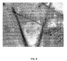
- FIG. 4 is the TEM and the picture of CIGS nanoparticles/wires
- FIG. 5 is the TEM of decomposed CIGS nanowires
- FIG. 6 is a diagram of the selenization temperature profile
- FIG. 7 is cross-sectional TEM of CIGSS films.
- FIG. 8 is the structure diagram and picture of CIGSS device.
- FIG. 1 shows the fabrication process of CIGSS photo-voltaic (“PV”) device.
- CIGS nanoparticles/wires have been synthesized using the low-cost solution route under atmospheric conditions in accordance with the present invention.
- the approach is simpler and less costly than any other non-vacuum methods with the following advantages:
- nanoparticles (3) Formation of amorphous and soluble nanoparticles/wires.
- the nanoparticles can be deposited on various substrates and turn into uniform thin films at low temperature ( ⁇ 350° C.);
- the amorphous CIGS nanoparticles fabricated in our invention melt under low temperature (even below 180V) and crystallize to various sizes of nanoparticles with increasing temperature (above 200° C.).
- Ultrasonic spraying CIGS ink on Mo glass substrate using ultrasonic spray to reduce the aggregation effect of CIGS nanoparticles/nanowires and obtaining uniform CIGS precursor films.
- the process of ultrasonic spraying CIGS-based ink on Mo-coated glass substrate, such as a glass substrate, includes the following steps illustrated in FIG. 3 :
- Preparing CIGSS device uses typical chemical bath deposition and sputtering and evaporating route.
- the whole process of fabricating CIGSS PV device includes the following detailed steps:
- a thickening solution B by: Adding Ethylcellulose (EC) (e.g. 0.3 g) into Terpinol (e.g. 10 mL), stirring overnight and heating to a temperature up to 200° C. until it is completely dissolved.
- Ethylcellulose e.g. 0.3 g
- Terpinol e.g. 10 mL
- CIGS dried powder e.g. 3.0 g
- solvent methyl ethyl ketone (“MEK”) e.g. 70 mL
- PEG e.g. 30 mL
- SHMP sodium hexametaphophate
- monodispersed CIGS ink e.g. 100 mL
- Ts under 300° C. (e.g. 100° C.);
- D less than 150 mm (e.g. 90 mm);
- the procedures of heating treatment are described.
- the process of heat treatment includes the following steps:
- FIG. 5 shown the nanowires begin to decompose under 150° C.
- the temperature is increased up to 500° C. (e.g. 350° C.) and held for half an hour, which will remove all the organic solvents and additives, finally the color changes to a deep black.
- FIG. 6 shows the selenization temperature profile.
- FIG. 8 shows the structure diagram and picture of CIGSS device made in accordance with the invention.
- the invention allows the drawbacks of the known non-vacuum techniques to be eliminated.
- the invention provides a method for preparing CIGSS absorber layers by using a metal salt, thickening and binding agents to form uniform nanoparticle and nanowire networks and to provide a finished high quality CIGSS film after selenization, in which:
- CIGS nanoparticles and nanowires are produced based on using a metal salt such as metal chloride and acetate at room temperature without inert gas protection;
- a CIGS precursor layer is coated on a Mo glass substrate by ultrasonic sprying of the CIGS nanoparticle and nanowire solution;
- a clean CIGS precursor layer is obtained by cleaning the residue salts and carbon agents at an increased temperature above 200° C.
- High quality CIGSS film is fabricated after selenizing the pretreated precursor layer at a temperature above 400° C.
Abstract
Description
Claims (14)
Priority Applications (2)
| Application Number | Priority Date | Filing Date | Title |
|---|---|---|---|
| US13/893,756 US9105798B2 (en) | 2013-05-14 | 2013-05-14 | Preparation of CIGS absorber layers using coated semiconductor nanoparticle and nanowire networks |
| US14/048,285 US20140342496A1 (en) | 2013-05-14 | 2013-12-16 | Preparation of cigs absorber layers using coated semiconductor nanoparticle and nanowire networks |
Applications Claiming Priority (1)
| Application Number | Priority Date | Filing Date | Title |
|---|---|---|---|
| US13/893,756 US9105798B2 (en) | 2013-05-14 | 2013-05-14 | Preparation of CIGS absorber layers using coated semiconductor nanoparticle and nanowire networks |
Related Child Applications (1)
| Application Number | Title | Priority Date | Filing Date |
|---|---|---|---|
| US14/048,285 Continuation US20140342496A1 (en) | 2013-05-14 | 2013-12-16 | Preparation of cigs absorber layers using coated semiconductor nanoparticle and nanowire networks |
Publications (2)
| Publication Number | Publication Date |
|---|---|
| US20140342495A1 US20140342495A1 (en) | 2014-11-20 |
| US9105798B2 true US9105798B2 (en) | 2015-08-11 |
Family
ID=51896089
Family Applications (2)
| Application Number | Title | Priority Date | Filing Date |
|---|---|---|---|
| US13/893,756 Active 2033-05-29 US9105798B2 (en) | 2013-05-14 | 2013-05-14 | Preparation of CIGS absorber layers using coated semiconductor nanoparticle and nanowire networks |
| US14/048,285 Abandoned US20140342496A1 (en) | 2013-05-14 | 2013-12-16 | Preparation of cigs absorber layers using coated semiconductor nanoparticle and nanowire networks |
Family Applications After (1)
| Application Number | Title | Priority Date | Filing Date |
|---|---|---|---|
| US14/048,285 Abandoned US20140342496A1 (en) | 2013-05-14 | 2013-12-16 | Preparation of cigs absorber layers using coated semiconductor nanoparticle and nanowire networks |
Country Status (1)
| Country | Link |
|---|---|
| US (2) | US9105798B2 (en) |
Families Citing this family (2)
| Publication number | Priority date | Publication date | Assignee | Title |
|---|---|---|---|---|
| CN106382757A (en) * | 2016-08-30 | 2017-02-08 | 吉林大学 | In-situ self-growth ultralow reflectivity material and preparing method thereof |
| CN107699870B (en) * | 2017-09-18 | 2020-01-21 | 中山大学 | Method for preparing film in supergravity chemical deposition tube and system required by same |
Citations (34)
| Publication number | Priority date | Publication date | Assignee | Title |
|---|---|---|---|---|
| US6258620B1 (en) * | 1997-10-15 | 2001-07-10 | University Of South Florida | Method of manufacturing CIGS photovoltaic devices |
| US6268014B1 (en) * | 1997-10-02 | 2001-07-31 | Chris Eberspacher | Method for forming solar cell materials from particulars |
| US20070111367A1 (en) * | 2005-10-19 | 2007-05-17 | Basol Bulent M | Method and apparatus for converting precursor layers into photovoltaic absorbers |
| US20080044570A1 (en) * | 2004-05-03 | 2008-02-21 | Solaronix Sa | Method for Producing a Thin-Film Chalcopyrite Compound |
| US20080149176A1 (en) * | 2004-09-18 | 2008-06-26 | Nanosolar Inc. | Coated nanoparticles and quantum dots for solution-based fabrication of photovoltaic cells |
| US20090145482A1 (en) * | 2007-12-06 | 2009-06-11 | Mitzi David B | Photovoltaic Device with Solution-processed Chalcogenide Absorber Layer |
| US20090214763A1 (en) * | 2008-02-27 | 2009-08-27 | Korea Institute Of Science And Technology | Preparation of thin film for solar cell using paste |
| US7604843B1 (en) * | 2005-03-16 | 2009-10-20 | Nanosolar, Inc. | Metallic dispersion |
| US20090260670A1 (en) * | 2008-04-18 | 2009-10-22 | Xiao-Chang Charles Li | Precursor ink for producing IB-IIIA-VIA semiconductors |
| WO2010085553A1 (en) | 2009-01-21 | 2010-07-29 | Purdue Research Foundation | Selenization of precursor layer containing culns2 nanoparticles |
| US20110008927A1 (en) * | 2007-12-29 | 2011-01-13 | Shanghai Institute Of Ceramics, Chinese Academy Of Sciences | Method for preparing light absorption layer of copper-indium-gallium-sulfur-selenium thin film solar cells |
| US20110065228A1 (en) * | 2009-09-15 | 2011-03-17 | Xiao-Chang Charles Li | Manufacture of thin solar cells based on ink printing technology |
| US7915072B1 (en) | 2009-11-19 | 2011-03-29 | Jenn Feng New Energy Co., Ltd. | Non-vacuum coating method for preparing light absorbing layer of solar cell |
| US7922804B2 (en) * | 2009-03-25 | 2011-04-12 | Jenn Feng Industrial Co., Ltd. | Method for preparing sol-gel solution for CIGS solar cell |
| US20110206599A1 (en) * | 2010-02-22 | 2011-08-25 | Keszler Douglas A | Metal chalcogenide aqueous precursors and processes to form metal chalcogenide films |
| US8048477B2 (en) * | 2004-02-19 | 2011-11-01 | Nanosolar, Inc. | Chalcogenide solar cells |
| US20110303122A1 (en) * | 2008-03-07 | 2011-12-15 | National Research Council Of Canada | Sterically bulky stabilizers |
| US8101498B2 (en) * | 2005-04-21 | 2012-01-24 | Pinnington Thomas Henry | Bonded intermediate substrate and method of making same |
| US20120061247A1 (en) * | 2010-09-09 | 2012-03-15 | International Business Machines Corporation | Method and Chemistry for Selenium Electrodeposition |
| US20120080091A1 (en) * | 2010-10-04 | 2012-04-05 | Byoung Koun Min | Fabrication of cis or cigs thin film for solar cells using paste or ink |
| US20120098032A1 (en) | 2010-10-25 | 2012-04-26 | Wei Guo | Non-vacuum method for fabrication of a photovoltaic absorber layer |
| US20120115312A1 (en) * | 2009-05-26 | 2012-05-10 | Purdue Research Foundation | Thin films for photovoltaic cells |
| US20120164762A1 (en) * | 2010-03-09 | 2012-06-28 | University Of Electronic Science And Technology Of China | Active matrix organic electroluminescent device and method of manufacture thereof |
| US8231848B1 (en) * | 2012-04-10 | 2012-07-31 | Sun Harmonics Ltd | One-pot synthesis of chalcopyrite-based semi-conductor nanoparticles |
| US20120192930A1 (en) * | 2011-02-02 | 2012-08-02 | Battelle Energy Alliance, Llc | Methods for forming particles, methods of forming semiconductor materials, methods of forming semiconductor devices, and devices formed using such methods |
| WO2012161401A1 (en) | 2011-05-25 | 2012-11-29 | Korea Institute Of Energy Research | METHOD OF MANUFACTURING DENSE CIGSe/CISe THIN FILM USING SELENIZATION OF CIGS/CIS NANOPARTICLES |
| US20120302002A1 (en) * | 2011-08-15 | 2012-11-29 | Stion Corporation | Method of Manufacture of Sodium Doped CIGS/CIGSS Absorber Layers for High Efficiency Photovoltaic Devices |
| US20130045565A1 (en) * | 2010-07-20 | 2013-02-21 | Se-Jin Ahn | Method of manufacturing high density cis thin film for solar cell and method of manufacturing thin film solar cell using the same |
| US20130059410A1 (en) * | 2004-02-19 | 2013-03-07 | Nanosolar, Inc. | Solution-Based Fabrication of Photovoltaic Cell |
| US20130171768A1 (en) * | 2011-12-30 | 2013-07-04 | Tsung-Shin Wu | Fabriation method for light absorption layer of solar cell |
| US20130206232A1 (en) * | 2010-07-12 | 2013-08-15 | Board Of Regents Of The University Of Texas System | Nanowires and methods of making and using |
| US20130230427A1 (en) * | 2009-08-19 | 2013-09-05 | Kuan-Jiuh Lin | Method for fabricating a biosensor chip and the biosensor chip made thereby |
| US20140109966A1 (en) * | 2012-10-24 | 2014-04-24 | Korea Institute Of Science And Technology | Bifacial thin film solar cell fabricated by paste coating method |
| US20140134791A1 (en) * | 2012-11-10 | 2014-05-15 | Sean Andrew Vail | Solution-Processed Metal-Selenide Semiconductor Using Selenium Nanoparticles |
-
2013
- 2013-05-14 US US13/893,756 patent/US9105798B2/en active Active
- 2013-12-16 US US14/048,285 patent/US20140342496A1/en not_active Abandoned
Patent Citations (35)
| Publication number | Priority date | Publication date | Assignee | Title |
|---|---|---|---|---|
| US6268014B1 (en) * | 1997-10-02 | 2001-07-31 | Chris Eberspacher | Method for forming solar cell materials from particulars |
| US20020006470A1 (en) * | 1997-10-02 | 2002-01-17 | Chris Eberspacher | Method for forming particulate materials |
| US6258620B1 (en) * | 1997-10-15 | 2001-07-10 | University Of South Florida | Method of manufacturing CIGS photovoltaic devices |
| US20130059410A1 (en) * | 2004-02-19 | 2013-03-07 | Nanosolar, Inc. | Solution-Based Fabrication of Photovoltaic Cell |
| US8048477B2 (en) * | 2004-02-19 | 2011-11-01 | Nanosolar, Inc. | Chalcogenide solar cells |
| US20080044570A1 (en) * | 2004-05-03 | 2008-02-21 | Solaronix Sa | Method for Producing a Thin-Film Chalcopyrite Compound |
| US20080149176A1 (en) * | 2004-09-18 | 2008-06-26 | Nanosolar Inc. | Coated nanoparticles and quantum dots for solution-based fabrication of photovoltaic cells |
| US7604843B1 (en) * | 2005-03-16 | 2009-10-20 | Nanosolar, Inc. | Metallic dispersion |
| US8101498B2 (en) * | 2005-04-21 | 2012-01-24 | Pinnington Thomas Henry | Bonded intermediate substrate and method of making same |
| US20070111367A1 (en) * | 2005-10-19 | 2007-05-17 | Basol Bulent M | Method and apparatus for converting precursor layers into photovoltaic absorbers |
| US20090145482A1 (en) * | 2007-12-06 | 2009-06-11 | Mitzi David B | Photovoltaic Device with Solution-processed Chalcogenide Absorber Layer |
| US20110008927A1 (en) * | 2007-12-29 | 2011-01-13 | Shanghai Institute Of Ceramics, Chinese Academy Of Sciences | Method for preparing light absorption layer of copper-indium-gallium-sulfur-selenium thin film solar cells |
| US20090214763A1 (en) * | 2008-02-27 | 2009-08-27 | Korea Institute Of Science And Technology | Preparation of thin film for solar cell using paste |
| US20110303122A1 (en) * | 2008-03-07 | 2011-12-15 | National Research Council Of Canada | Sterically bulky stabilizers |
| US20090260670A1 (en) * | 2008-04-18 | 2009-10-22 | Xiao-Chang Charles Li | Precursor ink for producing IB-IIIA-VIA semiconductors |
| WO2010085553A1 (en) | 2009-01-21 | 2010-07-29 | Purdue Research Foundation | Selenization of precursor layer containing culns2 nanoparticles |
| US7922804B2 (en) * | 2009-03-25 | 2011-04-12 | Jenn Feng Industrial Co., Ltd. | Method for preparing sol-gel solution for CIGS solar cell |
| US20120115312A1 (en) * | 2009-05-26 | 2012-05-10 | Purdue Research Foundation | Thin films for photovoltaic cells |
| US20130230427A1 (en) * | 2009-08-19 | 2013-09-05 | Kuan-Jiuh Lin | Method for fabricating a biosensor chip and the biosensor chip made thereby |
| US20110065228A1 (en) * | 2009-09-15 | 2011-03-17 | Xiao-Chang Charles Li | Manufacture of thin solar cells based on ink printing technology |
| US7915072B1 (en) | 2009-11-19 | 2011-03-29 | Jenn Feng New Energy Co., Ltd. | Non-vacuum coating method for preparing light absorbing layer of solar cell |
| US20110206599A1 (en) * | 2010-02-22 | 2011-08-25 | Keszler Douglas A | Metal chalcogenide aqueous precursors and processes to form metal chalcogenide films |
| US20120164762A1 (en) * | 2010-03-09 | 2012-06-28 | University Of Electronic Science And Technology Of China | Active matrix organic electroluminescent device and method of manufacture thereof |
| US20130206232A1 (en) * | 2010-07-12 | 2013-08-15 | Board Of Regents Of The University Of Texas System | Nanowires and methods of making and using |
| US20130045565A1 (en) * | 2010-07-20 | 2013-02-21 | Se-Jin Ahn | Method of manufacturing high density cis thin film for solar cell and method of manufacturing thin film solar cell using the same |
| US20120061247A1 (en) * | 2010-09-09 | 2012-03-15 | International Business Machines Corporation | Method and Chemistry for Selenium Electrodeposition |
| US20120080091A1 (en) * | 2010-10-04 | 2012-04-05 | Byoung Koun Min | Fabrication of cis or cigs thin film for solar cells using paste or ink |
| US20120098032A1 (en) | 2010-10-25 | 2012-04-26 | Wei Guo | Non-vacuum method for fabrication of a photovoltaic absorber layer |
| US20120192930A1 (en) * | 2011-02-02 | 2012-08-02 | Battelle Energy Alliance, Llc | Methods for forming particles, methods of forming semiconductor materials, methods of forming semiconductor devices, and devices formed using such methods |
| WO2012161401A1 (en) | 2011-05-25 | 2012-11-29 | Korea Institute Of Energy Research | METHOD OF MANUFACTURING DENSE CIGSe/CISe THIN FILM USING SELENIZATION OF CIGS/CIS NANOPARTICLES |
| US20120302002A1 (en) * | 2011-08-15 | 2012-11-29 | Stion Corporation | Method of Manufacture of Sodium Doped CIGS/CIGSS Absorber Layers for High Efficiency Photovoltaic Devices |
| US20130171768A1 (en) * | 2011-12-30 | 2013-07-04 | Tsung-Shin Wu | Fabriation method for light absorption layer of solar cell |
| US8231848B1 (en) * | 2012-04-10 | 2012-07-31 | Sun Harmonics Ltd | One-pot synthesis of chalcopyrite-based semi-conductor nanoparticles |
| US20140109966A1 (en) * | 2012-10-24 | 2014-04-24 | Korea Institute Of Science And Technology | Bifacial thin film solar cell fabricated by paste coating method |
| US20140134791A1 (en) * | 2012-11-10 | 2014-05-15 | Sean Andrew Vail | Solution-Processed Metal-Selenide Semiconductor Using Selenium Nanoparticles |
Non-Patent Citations (19)
| Title |
|---|
| A nanoparticle ink printing process for all printed thin film copper-indium-selenide (CIS) solar cells, X. Charles Li et al. Nanoscale Photonic and Cell Technologies for Photovoltaics, edited by Loucas Tsakalakos, Proc. of SPIE vol. 7047, 70470E, (2008) . 0277-786X/08/$18 . doi: 10.1117/12.794946. |
| A nanoparticle ink printing process for all printed thin film copper-indium-selenide (CIS) solar cells, X. Charles Li et al. Nanoscale Photonic and Cell Technologies for Photovoltaics, edited by Loucas Tsakalakos, Proc. of SPIE vol. 7047, 70470E, (2008) • 0277-786X/08/$18 • doi: 10.1117/12.794946. |
| Ahn et al., Nanoparticle derived Cu(In, Ga)Se2 absorber layer for thin film solar cells, Colloids and Surfaces A: Physicochem. Eng. Aspects 313-314 (2008) 171-174. * |
| Cu (In,Ga)Se2 thin films and solar cells prepared by selenization of metallic precursors Bülent M. Basol et al. Journal of Vacuum Science & Technology A / vol. 14 / Issue 4 (1996). |
| Development of a hybrid sputtering/evaporation process for Cu(In,Ga)Se2 thin film solar cells M. Acciarri et al. Crystal Research and Technology Special Issue: Italien Crystal Growth Conference 2010 (ICG2010) vol. 46, Issue 8, pp. 871-876, Aug. 2011. |
| Development of Low Cost CIGS Solar Cell MNRE Supported Project @ Moser Baer India Ltd R&D Conclave Aug. 9, 2012. |
| Fabrication of CuInGaSe2 Thin Film Solar Cells using Low-cost Air-stable Inks Wei Wang An Abstract of the Dissertation of Wei Wang for the degree of Doctor of Philosophy in Chemical Engineering presented on Jul. 5, 2012. |
| Ham et al., Preparing of CIGS nanoparticles using one step synthesis, 217th ECS Meeting, Abstract #338, © The Electrochemical Society. * |
| Improvement of Film Quality in CuInSe2 Thin Films Fabricated by a Non-Vacuum, Nanoparticle-Based Approach Yiwen Zhang et al. Japanese Journal of Applied Physics 50 (2011) 04DP12. |
| Isothermal and Two-Temperature Zone Selenization ofMo Layers L. Kaupmees et al. Hindawi Publishing Corporation Advances in Materials Science and Engineering vol. 2012, Article ID 345762,11 pages doi:10.1155/2012/345762. |
| Layer-by-Layer Nanoassembly of Copper Indium Gallium Selenium Nanoparticle Films for Solar Cell Applications A. Hemati et al. Journal of Nanomaterials vol. 2012 (2012), Article ID 512409, 6 pages doi:10.1155/2012/512409. |
| Nanoparticle derived Cu(In, Ga)Se2 absorber layer for thin film solar cells SeJin Ahn et al. Colloids and Surfaces A: Physicochemical and Engineering Aspects vols. 313-314, Feb. 1, 2008, pp. 171-174. |
| Nguyen et al., Making nanoparticle ink for compound solar cells, SPIE Newsroom: SPIE, 2013. * |
| Non-vacuum deposition of Cu(In,Ga)Se2 absorber layers from binder free, alcohol solutions, Alexander R. Uhl et al. Progress in Photovoltaics: Research and Applications Prog. Photovolt: Res. Appl. 2012; 20:526-533 Published online Jan. 31, 2012 in Wiley Online Library (wileyonlinelibrary.com). DOI: 10.1002/pip.1246. |
| Non-vacuum methods for formation of Cu(In,Ga)(Se, S)2 thin film photovoltaic absorbers C. J. Hibberd et al. Progress in Photovoltaics: Research and Applications Special Issue: Chalcopyrite Thin Film Solar Cells vol. 18, Issue 6, pp. 434-452, Sep. 2010. |
| Research Project , retrieved from website hunter.cuny.edu/physics/faculty/ren/repository/files/Project1.pdf. * |
| Wang et al., 8.01% CuInGaSe2 solar cells fabricated by air-stable low-cost inks, Phys. Chem. Chem. Phys., 2012, 14, 11154-11159. * |
| Wang et al., Inkjet printed chalcopyrite CulnxGa1-xSe2 thin film solar cells, Solar Energy Materials & Solar Cells 95 (2011) 2616-2620. * |
| Zhang et al., Fabrication and Characterization of Thin Film Solar Cell Made from Culn0.75Ga0.25S2 Wurtzite Nanoparticles, Hindawi Publishing Corporation, Journal of Nanomaterials, vol. 2013, Article ID 320375, 5 pages. * |
Also Published As
| Publication number | Publication date |
|---|---|
| US20140342495A1 (en) | 2014-11-20 |
| US20140342496A1 (en) | 2014-11-20 |
Similar Documents
| Publication | Publication Date | Title |
|---|---|---|
| JP5325874B2 (en) | Method for producing I-III-VI2 nanoparticles and method for producing polycrystalline light absorption layer thin film | |
| US8569102B2 (en) | Method of manufacturing high density CIS thin film for solar cell and method of manufacturing thin film solar cell using the same | |
| KR102037130B1 (en) | Inorganic Salt-Nanoparticle Ink for Thin Film Photovoltaic Devices and Related Methods | |
| US10170651B2 (en) | Metal-doped cu(In,Ga) (S,Se)2 nanoparticles | |
| US9893220B2 (en) | CIGS nanoparticle ink formulation having a high crack-free limit | |
| Patel et al. | Effect of type of solvent on the sol-gel spin coated CZTS thin films | |
| US9105798B2 (en) | Preparation of CIGS absorber layers using coated semiconductor nanoparticle and nanowire networks | |
| Patel et al. | Recent Developments in Cu2 (CZTS) Preparation, Optimization and its Application in Solar Cell Development and Photocatalytic Applications | |
| JP2019024106A (en) | Preparation of copper-rich copper indium (gallium) diselenide/disulphide | |
| JP2017212404A (en) | Method of manufacturing homogeneous coating liquid, method of manufacturing light-absorbing layer for solar battery, and method of manufacturing solar battery | |
| US20200343393A1 (en) | Alkali metal-incorporated chalcopyrite compound-based thin film and method of fabricating the same | |
| KR101137434B1 (en) | Preparation method for cis-based compound thin film by using rapid thermal processing and preparation method for thin film solarcell manufactured by using the cis-based compound thin film | |
| TWI675890B (en) | Cigs nanoparticle ink formulation with a high crack-free limit | |
| KR102379759B1 (en) | Manufacturing method of high quality photo-absorber by alloying alkali elements | |
| KR20130054800A (en) | Manufacturing method for thin film of absorber layer and thin film solar cell comprising it | |
| JP2011099059A (en) | Ink for producing compound semiconductor thin film, compound semiconductor thin film produced by using the same, solar cell having compound semiconductor thin film, and method of manufacturing solar cell | |
| Dhawale et al. | Solution processed CZTSSe thin film solar cell absorber: Ink formulation and characterization | |
| Plazaa et al. | Advances on CdTe thin film deposition using CdTe colloidal dispersions for photovoltaic applications | |
| KR101463327B1 (en) | Preparation Method of Copper Indium Diselenide Thin Film for Solar Cell Using Spray Process | |
| Frenia et al. | Development of Low-cost PV Devices by Using Nanocrystal Ink of Light-absorbing CIGS Semiconductor Layer |
Legal Events
| Date | Code | Title | Description |
|---|---|---|---|
| AS | Assignment |
Owner name: SUN HARMONICS LTD, A CHINESE CORPORATION HEREAFTER Free format text: ASSIGNMENT OF ASSIGNORS INTEREST;ASSIGNORS:REN, YUHANG;LUO, PAIFENG;GAO, BO;AND OTHERS;SIGNING DATES FROM 20130422 TO 20130423;REEL/FRAME:030554/0567 |
|
| STCF | Information on status: patent grant |
Free format text: PATENTED CASE |
|
| FEPP | Fee payment procedure |
Free format text: SURCHARGE FOR LATE PAYMENT, SMALL ENTITY (ORIGINAL EVENT CODE: M2554); ENTITY STATUS OF PATENT OWNER: SMALL ENTITY |
|
| MAFP | Maintenance fee payment |
Free format text: PAYMENT OF MAINTENANCE FEE, 4TH YR, SMALL ENTITY (ORIGINAL EVENT CODE: M2551); ENTITY STATUS OF PATENT OWNER: SMALL ENTITY Year of fee payment: 4 |
|
| MAFP | Maintenance fee payment |
Free format text: PAYMENT OF MAINTENANCE FEE, 8TH YR, SMALL ENTITY (ORIGINAL EVENT CODE: M2552); ENTITY STATUS OF PATENT OWNER: SMALL ENTITY Year of fee payment: 8 |