US9116834B2 - Methods and apparatus for calculating electromagnetic scattering properties of a structure and for reconstruction of approximate structures - Google Patents
Methods and apparatus for calculating electromagnetic scattering properties of a structure and for reconstruction of approximate structures Download PDFInfo
- Publication number
- US9116834B2 US9116834B2 US13/417,759 US201213417759A US9116834B2 US 9116834 B2 US9116834 B2 US 9116834B2 US 201213417759 A US201213417759 A US 201213417759A US 9116834 B2 US9116834 B2 US 9116834B2
- Authority
- US
- United States
- Prior art keywords
- electromagnetic
- field
- scattering property
- normal
- current density
- Prior art date
- Legal status (The legal status is an assumption and is not a legal conclusion. Google has not performed a legal analysis and makes no representation as to the accuracy of the status listed.)
- Active, expires
Links
Images


Classifications
-
- H—ELECTRICITY
- H01—ELECTRIC ELEMENTS
- H01L—SEMICONDUCTOR DEVICES NOT COVERED BY CLASS H10
- H01L21/00—Processes or apparatus adapted for the manufacture or treatment of semiconductor or solid state devices or of parts thereof
- H01L21/02—Manufacture or treatment of semiconductor devices or of parts thereof
- H01L21/027—Making masks on semiconductor bodies for further photolithographic processing not provided for in group H01L21/18 or H01L21/34
- H01L21/0271—Making masks on semiconductor bodies for further photolithographic processing not provided for in group H01L21/18 or H01L21/34 comprising organic layers
- H01L21/0273—Making masks on semiconductor bodies for further photolithographic processing not provided for in group H01L21/18 or H01L21/34 comprising organic layers characterised by the treatment of photoresist layers
- H01L21/0274—Photolithographic processes
-
- G—PHYSICS
- G01—MEASURING; TESTING
- G01N—INVESTIGATING OR ANALYSING MATERIALS BY DETERMINING THEIR CHEMICAL OR PHYSICAL PROPERTIES
- G01N21/00—Investigating or analysing materials by the use of optical means, i.e. using sub-millimetre waves, infrared, visible or ultraviolet light
- G01N21/17—Systems in which incident light is modified in accordance with the properties of the material investigated
- G01N21/47—Scattering, i.e. diffuse reflection
- G01N21/4788—Diffraction
-
- G—PHYSICS
- G01—MEASURING; TESTING
- G01N—INVESTIGATING OR ANALYSING MATERIALS BY DETERMINING THEIR CHEMICAL OR PHYSICAL PROPERTIES
- G01N21/00—Investigating or analysing materials by the use of optical means, i.e. using sub-millimetre waves, infrared, visible or ultraviolet light
- G01N21/84—Systems specially adapted for particular applications
- G01N21/88—Investigating the presence of flaws or contamination
- G01N21/95—Investigating the presence of flaws or contamination characterised by the material or shape of the object to be examined
- G01N21/956—Inspecting patterns on the surface of objects
- G01N21/95607—Inspecting patterns on the surface of objects using a comparative method
-
- G—PHYSICS
- G03—PHOTOGRAPHY; CINEMATOGRAPHY; ANALOGOUS TECHNIQUES USING WAVES OTHER THAN OPTICAL WAVES; ELECTROGRAPHY; HOLOGRAPHY
- G03F—PHOTOMECHANICAL PRODUCTION OF TEXTURED OR PATTERNED SURFACES, e.g. FOR PRINTING, FOR PROCESSING OF SEMICONDUCTOR DEVICES; MATERIALS THEREFOR; ORIGINALS THEREFOR; APPARATUS SPECIALLY ADAPTED THEREFOR
- G03F1/00—Originals for photomechanical production of textured or patterned surfaces, e.g., masks, photo-masks, reticles; Mask blanks or pellicles therefor; Containers specially adapted therefor; Preparation thereof
- G03F1/68—Preparation processes not covered by groups G03F1/20 - G03F1/50
- G03F1/82—Auxiliary processes, e.g. cleaning or inspecting
- G03F1/84—Inspecting
-
- G—PHYSICS
- G03—PHOTOGRAPHY; CINEMATOGRAPHY; ANALOGOUS TECHNIQUES USING WAVES OTHER THAN OPTICAL WAVES; ELECTROGRAPHY; HOLOGRAPHY
- G03F—PHOTOMECHANICAL PRODUCTION OF TEXTURED OR PATTERNED SURFACES, e.g. FOR PRINTING, FOR PROCESSING OF SEMICONDUCTOR DEVICES; MATERIALS THEREFOR; ORIGINALS THEREFOR; APPARATUS SPECIALLY ADAPTED THEREFOR
- G03F7/00—Photomechanical, e.g. photolithographic, production of textured or patterned surfaces, e.g. printing surfaces; Materials therefor, e.g. comprising photoresists; Apparatus specially adapted therefor
- G03F7/70—Microphotolithographic exposure; Apparatus therefor
- G03F7/70483—Information management; Active and passive control; Testing; Wafer monitoring, e.g. pattern monitoring
- G03F7/70491—Information management, e.g. software; Active and passive control, e.g. details of controlling exposure processes or exposure tool monitoring processes
- G03F7/705—Modelling or simulating from physical phenomena up to complete wafer processes or whole workflow in wafer productions
-
- G—PHYSICS
- G03—PHOTOGRAPHY; CINEMATOGRAPHY; ANALOGOUS TECHNIQUES USING WAVES OTHER THAN OPTICAL WAVES; ELECTROGRAPHY; HOLOGRAPHY
- G03F—PHOTOMECHANICAL PRODUCTION OF TEXTURED OR PATTERNED SURFACES, e.g. FOR PRINTING, FOR PROCESSING OF SEMICONDUCTOR DEVICES; MATERIALS THEREFOR; ORIGINALS THEREFOR; APPARATUS SPECIALLY ADAPTED THEREFOR
- G03F7/00—Photomechanical, e.g. photolithographic, production of textured or patterned surfaces, e.g. printing surfaces; Materials therefor, e.g. comprising photoresists; Apparatus specially adapted therefor
- G03F7/70—Microphotolithographic exposure; Apparatus therefor
- G03F7/70483—Information management; Active and passive control; Testing; Wafer monitoring, e.g. pattern monitoring
- G03F7/70605—Workpiece metrology
- G03F7/70616—Monitoring the printed patterns
- G03F7/70625—Dimensions, e.g. line width, critical dimension [CD], profile, sidewall angle or edge roughness
-
- G—PHYSICS
- G06—COMPUTING; CALCULATING OR COUNTING
- G06F—ELECTRIC DIGITAL DATA PROCESSING
- G06F17/00—Digital computing or data processing equipment or methods, specially adapted for specific functions
- G06F17/10—Complex mathematical operations
- G06F17/11—Complex mathematical operations for solving equations, e.g. nonlinear equations, general mathematical optimization problems
-
- G06F17/50—
-
- G—PHYSICS
- G06—COMPUTING; CALCULATING OR COUNTING
- G06F—ELECTRIC DIGITAL DATA PROCESSING
- G06F30/00—Computer-aided design [CAD]
Definitions
- the present invention relates to calculation of electromagnetic scattering properties of structures.
- the invention may be applied for example in metrology of microscopic structures, for example to assess critical dimensions (CD) performance of a lithographic apparatus.
- CD critical dimensions
- a lithographic apparatus is a machine that applies a desired pattern onto a substrate, usually onto a target portion of the substrate.
- a lithographic apparatus can be used, for example, in the manufacture of integrated circuits (ICs).
- a patterning device which is alternatively referred to as a mask or a reticle, may be used to generate a circuit pattern to be formed on an individual layer of the IC.
- This pattern can be transferred onto a target portion (e.g., comprising part of, one, or several dies) on a substrate (e.g., a silicon wafer). Transfer of the pattern is typically via imaging onto a layer of radiation-sensitive material (resist) provided on the substrate.
- resist radiation-sensitive material
- a single substrate will contain a network of adjacent target portions that are successively patterned.
- lithographic apparatus include so-called steppers, in which each target portion is irradiated by exposing an entire pattern onto the target portion at one time, and so-called scanners, in which each target portion is irradiated by scanning the pattern through a radiation beam in a given direction (the “scanning”-direction) while synchronously scanning the substrate parallel or anti-parallel to this direction. It is also possible to transfer the pattern from the patterning device to the substrate by imprinting the pattern onto the substrate.
- a scatterometer in which a beam of radiation is directed onto a target on the surface of the substrate and properties of the scattered or reflected beam are measured. By comparing the properties of the beam before and after it has been reflected or scattered by the substrate, the properties of the substrate can be determined. This can be done, for example, by comparing the reflected beam with data stored in a library of known measurements associated with known substrate properties.
- Two main types of scatterometer are known.
- Spectroscopic scatterometers direct a broadband radiation beam onto the substrate and measure the spectrum (intensity as a function of wavelength) of the radiation scattered into a particular narrow angular range.
- Angularly resolved scatterometers use a monochromatic radiation beam and measure the intensity of the scattered radiation as a function of angle.
- CD reconstruction belongs to a group of problems known under the general name of inverse scattering, in which observed data is matched to a possible physical situation. The aim is to find a physical situation that gives rise to the observed data as closely as possible.
- the electromagnetic theory Maxwell's equations
- the inverse scattering problem is now to find the proper physical situation that corresponds to the actual measured data, which is typically a highly nonlinear problem.
- a nonlinear solver is used that uses the solutions of many forward scattering problems.
- the nonlinear problem is founded on three ingredients:
- the CSI employs a formulation in which the data mismatch and the mismatch in the Maxwell equations are solved simultaneously, i.e. the Maxwell equations are not solved to sufficient precision at each step of the minimization. Further, the CSI employs a pixilated image instead of parameterized shapes.
- the success of the CSI is largely due to the reformulation of the inverse problem in terms of the so-called contrast source J and the contrast function ⁇ as the fundamental unknowns.
- This reformulation makes the mismatch in the measured data independent of ⁇ and a linear problem in J, whereas the mismatch in the Maxwell equations remains nonlinear due to the coupling in ⁇ and J.
- the CSI was successfully combined with a volume-integral method (VIM) [14], a finite element method (FEM) [15], and a finite difference (FD) [16] method.
- VIP volume-integral method
- FEM finite element method
- FD finite difference
- all the underlying numerical methods (VIM, FEM, FD) are based on spatial formulations and spatial discretizations (i.e. pixels or meshes).
- a method of calculating electromagnetic scattering properties of a structure comprising: numerically solving a volume integral equation for a contrast current density by determining components of the contrast current density by using a field-material interaction operator to operate on a continuous component of the electromagnetic field and a continuous component of a scaled electromagnetic flux density corresponding to the electromagnetic field, the scaled electromagnetic flux density being formed as a scaled sum of discontinuous components of the electromagnetic field and of the contrast current density; and calculating electromagnetic scattering properties of the structure using the determined components of the contrast current density.
- a method of reconstructing an approximate structure of an object from a detected electromagnetic scattering property arising from illumination of the object by radiation comprising the steps: estimating at least one structural parameter; determining at least one model electromagnetic scattering property from the at least one structural parameter; comparing the detected electromagnetic scattering property to the at least one model electromagnetic scattering property; and determining an approximate object structure based on the result of the comparison, wherein the model electromagnetic scattering property is determined using a method according to the first aspect.
- an inspection apparatus for reconstructing an approximate structure of an object
- the inspection apparatus comprising: an illumination system configured to illuminate the object with radiation; a detection system configured to detect an electromagnetic scattering property arising from the illumination; a processor configured to estimate at least one structural parameter, determine at least one model electromagnetic scattering property from the at least one structural parameter, compare the detected electromagnetic scattering property to the at least one model electromagnetic scattering property and determine an approximate object structure from a difference between the detected electromagnetic scattering property and the at least one model electromagnetic scattering property, wherein the processor is configured to determine the model electromagnetic scattering property using a method according to the first aspect.
- a computer program product containing one or more sequences of machine-readable instructions for calculating electromagnetic scattering properties of a structure, the instructions being adapted to cause one or more processors to perform a method according to the first aspect.
- FIG. 1 depicts a lithographic apparatus.
- FIG. 2 depicts a lithographic cell or cluster.
- FIG. 3 depicts a first scatterometer
- FIG. 4 depicts a second scatterometer.
- FIG. 5 depicts a first example process using an embodiment of the invention for reconstruction of a structure from scatterometer measurements.
- FIG. 6 depicts a second example process using an embodiment of the invention for reconstruction of a structure from scatterometer measurements.
- FIG. 7 depicts the scattering geometry that may be reconstructed in accordance with an embodiment of the present invention.
- FIG. 8 depicts the structure of the background.
- FIG. 9 illustrates use of a Green's function to calculate the interaction of the scattered field with the layered medium.
- FIG. 10 is a flow chart of the high level method of solving the linear system corresponding to the VIM formula for the contrast current density.
- FIG. 11 is a flow chart of the computation of update vectors using the VIM formula for the contrast current density as known in the prior art.
- FIG. 12 depicts an embodiment of the present invention.
- FIG. 13 a is a flow chart of the computation of update vectors in accordance with an embodiment of present invention.
- FIG. 13 b is a flow chart of the matrix-vector product for the contrast current density used in solving the VIM formula with contrast source inversion in accordance with an embodiment of present invention.
- FIG. 13 c is a flow chart of the operation of material and projection operators used in the matrix-vector product of FIG. 13 b.
- FIG. 14 is a flow chart of a method of calculating electromagnetic scattering properties of a structure in accordance with an embodiment of present invention.
- FIG. 15 a is a definition of global (x, y) and local (x′′, y′′) coordinate systems for the rotated ellipse with offset c 0 .
- FIG. 15 b illustrates a NV field for the elliptical coordinate system.
- FIG. 15 c illustrates conformal mapping for an ellipse.
- FIG. 16 a illustrates continuous NV field for the rectangle.
- FIG. 16 b illustrates discontinuous NV field for the rectangle.
- FIG. 17 illustrates meshing a ‘dogbone’ in elementary shapes.
- FIG. 18 illustrates building the normal-vector field of a prism with a cross section of a rounded rectangle from smaller rectangles and circle segments in accordance with an embodiment of the present invention.
- FIG. 19 illustrates rotated and shifted triangle with NV field and local coordinate system.
- FIG. 20 illustrates a rotated and shifted trapezoid with NV field and local coordinate system.
- FIG. 21 illustrates rotated and shifted circle segment with NV field and local coordinate system.
- FIG. 22 depicts a procedure to approximate an ellipse by a staircased approximation
- FIG. 23 depicts in schematic form a computer system configured with programs and data in order to execute a method in accordance with an embodiment of the present invention.
- Embodiments of the invention may be implemented in hardware, firmware, software, or any combination thereof. Embodiments of the invention may also be implemented as instructions stored on a machine-readable medium, which may be read and executed by one or more processors.
- a machine-readable medium may include any mechanism for storing or transmitting information in a form readable by a machine (e.g., a computing device).
- a machine-readable medium may include read only memory (ROM); random access memory (RAM); magnetic disk storage media; optical storage media; flash memory devices; electrical, optical, acoustical or other forms of propagated signals (e.g., carrier waves, infrared signals, digital signals, etc.), and others.
- firmware, software, routines, instructions may be described herein as performing certain actions. However, it should be appreciated that such descriptions are merely for convenience and that such actions in fact result from computing devices, processors, controllers, or other devices executing the firmware, software, routines, instructions, etc.
- FIG. 1 schematically depicts a lithographic apparatus.
- the apparatus comprises: an illumination system (illuminator) IL configured to condition a radiation beam B (e.g., UV radiation or DUV radiation), a support structure (e.g., a mask table) MT constructed to support a patterning device (e.g., a mask) MA and connected to a first positioner PM configured to accurately position the patterning device in accordance with certain parameters, a substrate table (e.g., a wafer table) WT constructed to hold a substrate (e.g., a resist-coated wafer) W and connected to a second positioner PW configured to accurately position the substrate in accordance with certain parameters, and a projection system (e.g., a refractive projection lens system) PL configured to project a pattern imparted to the radiation beam B by patterning device MA onto a target portion C (e.g., comprising one or more dies) of the substrate W.
- a radiation beam B e.g.,
- the illumination system may include various types of optical components, such as refractive, reflective, magnetic, electromagnetic, electrostatic or other types of optical components, or any combination thereof, for directing, shaping, or controlling radiation.
- optical components such as refractive, reflective, magnetic, electromagnetic, electrostatic or other types of optical components, or any combination thereof, for directing, shaping, or controlling radiation.
- the support structure supports, i.e. bears the weight of, the patterning device. It holds the patterning device in a manner that depends on the orientation of the patterning device, the design of the lithographic apparatus, and other conditions, such as for example whether or not the patterning device is held in a vacuum environment.
- the support structure can use mechanical, vacuum, electrostatic or other clamping techniques to hold the patterning device.
- the support structure may be a frame or a table, for example, which may be fixed or movable as required.
- the support structure may ensure that the patterning device is at a desired position, for example with respect to the projection system. Any use of the terms “reticle” or “mask” herein may be considered synonymous with the more general term “patterning device.”
- patterning device used herein should be broadly interpreted as referring to any device that can be used to impart a radiation beam with a pattern in its cross-section such as to create a pattern in a target portion of the substrate. It should be noted that the pattern imparted to the radiation beam may not exactly correspond to the desired pattern in the target portion of the substrate, for example if the pattern includes phase-shifting features or so called assist features. Generally, the pattern imparted to the radiation beam will correspond to a particular functional layer in a device being created in the target portion, such as an integrated circuit.
- the patterning device may be transmissive or reflective.
- Examples of patterning devices include masks, programmable mirror arrays, and programmable LCD panels.
- Masks are well known in lithography, and include mask types such as binary, alternating phase-shift, and attenuated phase-shift, as well as various hybrid mask types.
- An example of a programmable mirror array employs a matrix arrangement of small mirrors, each of which can be individually tilted so as to reflect an incoming radiation beam in different directions. The tilted mirrors impart a pattern in a radiation beam, which is-reflected by the mirror matrix.
- projection system used herein should be broadly interpreted as encompassing any type of projection system, including refractive, reflective, catadioptric, magnetic, electromagnetic and electrostatic optical systems, or any combination thereof, as appropriate for the exposure radiation being used, or for other factors such as the use of an immersion liquid or the use of a vacuum. Any use of the term “projection lens” herein may be considered as synonymous with the more general term “projection system”.
- the apparatus is of a transmissive type (e.g., employing a transmissive mask).
- the apparatus may be of a reflective type (e.g., employing a programmable mirror array of a type as referred to above, or employing a reflective mask).
- the lithographic apparatus may be of a type having two (dual stage) or more substrate tables (and/or two or more mask tables). In such “multiple stage” machines the additional tables may be used in parallel, or preparatory steps may be carried out on one or more tables while one or more other tables are being used for exposure.
- the lithographic apparatus may also be of a type wherein at least a portion of the substrate may be covered by a liquid having a relatively high refractive index, e.g., water, so as to fill a space between the projection system and the substrate.
- a liquid having a relatively high refractive index e.g., water
- An immersion liquid may also be applied to other spaces in the lithographic apparatus, for example, between the mask and the projection system. Immersion techniques are well known in the art for increasing the numerical aperture of projection systems.
- immersion as used herein does not mean that a structure, such as a substrate, must be submerged in liquid, but rather only means that liquid is located between the projection system and the substrate during exposure.
- the illuminator IL receives a radiation beam from a radiation source SO.
- the source and the lithographic apparatus may be separate entities, for example when the source is an excimer laser. In such cases, the source is not considered to form part of the lithographic apparatus and the radiation beam is passed from the source SO to the illuminator IL with the aid of a beam delivery system BD comprising, for example, suitable directing mirrors and/or a beam expander. In other cases the source may be an integral part of the lithographic apparatus, for example when the source is a mercury lamp.
- the source SO and the illuminator IL, together with the beam delivery system BD if required, may be referred to as a radiation system.
- the illuminator IL may comprise an adjuster AD for adjusting the angular intensity distribution of the radiation beam.
- an adjuster AD for adjusting the angular intensity distribution of the radiation beam.
- the illuminator IL may comprise various other components, such as an integrator IN and a condenser CO.
- the illuminator may be used to condition the radiation beam, to have a desired uniformity and intensity distribution in its cross-section.
- the radiation beam B is incident on the patterning device (e.g., mask MA), which is held on the support structure (e.g., mask table MT), and is patterned by the patterning device. Having traversed the mask MA, the radiation beam B passes through the projection system PL, which focuses the beam onto a target portion C of the substrate W.
- the substrate table WT can be moved accurately, e.g., so as to position different target portions C in the path of the radiation beam B.
- the first positioner PM and another position sensor (which is not explicitly depicted in FIG.
- the mask table MT can be used to accurately position the mask MA with respect to the path of the radiation beam B, e.g., after mechanical retrieval from a mask library, or during a scan.
- movement of the mask table MT may be realized with the aid of a long-stroke module (coarse positioning) and a short-stroke module (fine positioning), which form part of the first positioner PM.
- movement of the substrate table WT may be realized using a long-stroke module and a short-stroke module, which form part of the second positioner PW.
- the mask table MT may be connected to a short-stroke actuator only, or may be fixed.
- Mask MA and substrate W may be aligned using mask alignment marks M 1 , M 2 and substrate alignment marks P 1 , P 2 .
- the substrate alignment marks as illustrated occupy dedicated target portions, they may be located in spaces between target portions (these are known as scribe-lane alignment marks).
- the mask alignment marks may be located between the dies.
- the depicted apparatus could be used in at least one of the following modes:
- the lithographic apparatus LA forms part of a lithographic cell LC, also sometimes referred to a lithocell or cluster, which also includes apparatus to perform pre- and post-exposure processes on a substrate.
- lithographic cell LC also sometimes referred to a lithocell or cluster
- apparatus to perform pre- and post-exposure processes on a substrate include spin coaters SC to deposit resist layers, developers DE to develop exposed resist, chill plates CH and bake plates BK.
- a substrate handler, or robot, RO picks up substrates from input/output ports I/O 1 , I/O 2 , moves them between the different process apparatus and delivers then to the loading bay LB of the lithographic apparatus.
- track control unit TCU which is itself controlled by the supervisory control system SCS, which also controls the lithographic apparatus via lithography control unit LACU.
- SCS supervisory control system
- LACU lithography control unit
- the substrates that are exposed by the lithographic apparatus are exposed correctly and consistently, it is desirable to inspect exposed substrates to measure properties such as overlay errors between subsequent layers, line thicknesses, critical dimensions (CD), etc. If errors are detected, adjustments may be made to exposures of subsequent substrates, especially if the inspection can be done soon and fast enough that other substrates of the same batch are still to be exposed. Also, already exposed substrates may be stripped and reworked—to improve yield—or discarded, thereby avoiding performing exposures on substrates that are known to be faulty. In a case where only some target portions of a substrate are faulty, further exposures can be performed only on those target portions which are good.
- properties such as overlay errors between subsequent layers, line thicknesses, critical dimensions (CD), etc. If errors are detected, adjustments may be made to exposures of subsequent substrates, especially if the inspection can be done soon and fast enough that other substrates of the same batch are still to be exposed. Also, already exposed substrates may be stripped and reworked—to improve yield—or
- An inspection apparatus is used to determine the properties of the substrates, and in particular, how the properties of different substrates or different layers of the same substrate vary from layer to layer.
- the inspection apparatus may be integrated into the lithographic apparatus LA or the lithocell LC or may be a stand-alone device. To enable most rapid measurements, it is desirable that the inspection apparatus measure properties in the exposed resist layer immediately after the exposure.
- the latent image in the resist has a very low contrast—there is only a very small difference in refractive index between the parts of the resist which have been exposed to radiation and those which have not—and not all inspection apparatus have sufficient sensitivity to make useful measurements of the latent image.
- measurements may be taken after the post-exposure bake step (PEB) which is customarily the first step carried out on exposed substrates and increases the contrast between exposed and unexposed parts of the resist.
- PEB post-exposure bake step
- the image in the resist may be referred to as semi-latent. It is also possible to make measurements of the developed resist image—at which point either the exposed or unexposed parts of the resist have been removed—or after a pattern transfer step such as etching. The latter possibility limits the possibilities for rework of faulty substrates but may still provide useful information.
- FIG. 3 depicts a scatterometer which may be used in an embodiment of the present invention. It comprises a broadband (white light) radiation projector 2 which projects radiation onto a substrate W. The reflected radiation is passed to a spectrometer detector 4 , which measures a spectrum 10 (intensity as a function of wavelength) of the specular reflected radiation. From this data, the structure or profile giving rise to the detected spectrum may be reconstructed by processing unit PU, e.g., conventionally by Rigorous Coupled Wave Analysis (RCWA) and non-linear regression or by comparison with a library of simulated spectra as shown at the bottom of FIG. 3 .
- RCWA Rigorous Coupled Wave Analysis
- Such a scatterometer may be configured as a normal-incidence scatterometer or an oblique-incidence scatterometer.
- FIG. 4 Another scatterometer that may be used in an embodiment of the present invention is shown in FIG. 4 .
- the radiation emitted by radiation source 2 is focused using lens system 12 through interference filter 13 and polarizer 17 , reflected by partially reflected surface 16 and is focused onto substrate W via a microscope objective lens 15 , which has a high numerical aperture (NA), preferably at least 0.9 and more preferably at least 0.95.
- NA numerical aperture
- Immersion scatterometers may even have lenses with numerical apertures over 1.
- the reflected radiation then transmits through partially reflective surface 16 into a detector 18 in order to have the scatter spectrum detected.
- the detector may be located in the back-projected pupil plane 11 , which is at the focal length of the lens system 15 , however the pupil plane may instead be re-imaged with auxiliary optics (not shown) onto the detector.
- the pupil plane is the plane in which the radial position of radiation defines the angle of incidence and the angular position defines azimuth angle of the radiation.
- the detector is preferably a two-dimensional detector so that a two-dimensional angular scatter spectrum of a substrate target 30 can be measured.
- the detector 18 may be, for example, an array of CCD or CMOS sensors, and may use an integration time of, for example, 40 milliseconds per frame.
- a reference beam is often used for example to measure the intensity of the incident radiation. To do this, when the radiation beam is incident on the beam splitter 16 part of it is transmitted through the beam splitter as a reference beam towards a reference mirror 14 . The reference beam is then projected onto a different part of the same detector 18 .
- a set of interference filters 13 is available to select a wavelength of interest in the range of, say, 405-790 nm or even lower, such as 200-300 nm.
- the interference filter may be tunable rather than comprising a set of different filters.
- a grating could be used instead of interference filters.
- the detector 18 may measure the intensity of scattered light at a single wavelength (or narrow wavelength range), the intensity separately at multiple wavelengths or integrated over a wavelength range. Furthermore, the detector may separately measure the intensity of transverse magnetic- and transverse electric-polarized light and/or the phase difference between the transverse magnetic- and transverse electric-polarized light.
- a broadband light source i.e. one with a wide range of light frequencies or wavelengths—and therefore of colors
- the plurality of wavelengths in the broadband preferably each has a bandwidth of ⁇ and a spacing of at least 2 ⁇ (i.e., twice the bandwidth).
- sources can be different portions of an extended radiation source which have been split using fiber bundles. In this way, angle resolved scatter spectra can be measured at multiple wavelengths in parallel.
- a 3-D spectrum (wavelength and two different angles) can be measured, which contains more information than a 2-D spectrum. This allows more information to be measured which increases metrology process robustness. This is described in more detail in EP1,628,164A, which is incorporated by reference herein in its entirety.
- the target 30 on substrate W may be a grating, which is printed such that after development, the bars are formed of solid resist lines.
- the bars may alternatively be etched into the substrate.
- This pattern is sensitive to chromatic aberrations in the lithographic projection apparatus, particularly the projection system PL, and illumination symmetry and the presence of such aberrations will manifest themselves in a variation in the printed grating. Accordingly, the scatterometry data of the printed gratings is used to reconstruct the gratings.
- the parameters of the grating such as line widths and shapes, may be input to the reconstruction process, performed by processing unit PU, from knowledge of the printing step and/or other scatterometry processes.
- the target is on the surface of the substrate.
- This target will often take the shape of a series of lines in a grating or substantially rectangular structures in a 2-D array.
- the purpose of rigorous optical diffraction theories in metrology is effectively the calculation of a diffraction spectrum that is reflected from the target.
- target shape information is obtained for CD (critical dimension) uniformity and overlay metrology.
- Overlay metrology is a measuring system in which the overlay of two targets is measured in order to determine whether two layers on a substrate are aligned or not.
- CD uniformity is simply a measurement of the uniformity of the grating on the spectrum to determine how the exposure system of the lithographic apparatus is functioning.
- CD critical dimension
- CD is the width of the object that is “written” on the substrate and is the limit at which a lithographic apparatus is physically able to write on a substrate.
- a diffraction pattern based on a first estimate of the target shape (a first candidate structure) is calculated and compared with the observed diffraction pattern. Parameters of the model are then varied systematically and the diffraction re-calculated in a series of iterations, to generate new candidate structures and so arrive at a best fit.
- a second type of process represented by FIG. 5
- diffraction spectra for many different candidate structures are calculated in advance to create a ‘library’ of diffraction spectra. Then the diffraction pattern observed from the measurement target is compared with the library of calculated spectra to find a best fit. Both methods can be used together: a coarse fit can be obtained from a library, followed by an iterative process to find a best fit.
- the target will be assumed for this description to be a 1-dimensionally (1-D) periodic structure. In practice it may be 2-dimensionally periodic, and the processing will be adapted accordingly.
- step 502 the diffraction pattern of the actual target on the substrate is measured using a scatterometer such as those described above.
- This measured diffraction pattern is forwarded to a calculation system such as a computer.
- the calculation system may be the processing unit PU referred to above, or it may be a separate apparatus.
- a ‘model recipe’ is established which defines a parameterized model of the target structure in terms of a number of parameters p i (p 1 , p 2 , p 3 and so on). These parameters may represent for example, in a 1D periodic structure, the angle of a side wall, the height or depth of a feature, the width of the feature. Properties of the target material and underlying layers are also represented by parameters such as refractive index (at a particular wavelength present in the scatterometry radiation beam). Specific examples will be given below. Importantly, while a target structure may be defined by dozens of parameters describing its shape and material properties, the model recipe will define many of these to have fixed values, while others are to be variable or ‘floating’ parameters for the purpose of the following process steps.
- a model target shape is estimated by setting initial values p i (0) for the floating parameters (i.e. p 1 (0) , p 2 (0) , p 3 (0) and so on). Each floating parameter will be generated within certain predetermined ranges, as defined in the recipe.
- step 506 the parameters representing the estimated shape, together with the optical properties of the different elements of the model, are used to calculate the scattering properties, for example using a rigorous optical diffraction method such as RCWA or any other solver of Maxwell equations. This gives an estimated or model diffraction pattern of the estimated target shape.
- a rigorous optical diffraction method such as RCWA or any other solver of Maxwell equations.
- steps 508 and 510 the measured diffraction pattern and the model diffraction pattern are then compared and their similarities and differences are used to calculate a “merit function” for the model target shape.
- step 512 assuming that the merit function indicates that the model needs to be improved before it represents accurately the actual target shape, new parameters p 1 (1) , p 2 (1) , p 3 (1) , etc. are estimated and fed back iteratively into step 506 . Steps 506 - 512 are repeated.
- the calculations in step 506 may further generate partial derivatives of the merit function, indicating the sensitivity with which increasing or decreasing a parameter will increase or decrease the merit function, in this particular region in the parameter space.
- the calculation of merit functions and the use of derivatives is generally known in the art, and will not be described here in detail.
- step 514 when the merit function indicates that this iterative process has converged on a solution with a desired accuracy, the currently estimated parameters are reported as the measurement of the actual target structure.
- the computation time of this iterative process is largely determined by the forward diffraction model used, i.e., the calculation of the estimated model diffraction pattern using a rigorous optical diffraction theory from the estimated target structure. If more parameters are required, then there are more degrees of freedom. The calculation time increases in principle with the power of the number of degrees of freedom.
- the estimated or model diffraction pattern calculated at 506 can be expressed in various forms. Comparisons are simplified if the calculated pattern is expressed in the same form as the measured pattern generated in step 510 .
- a modeled spectrum can be compared easily with a spectrum measured by the apparatus of FIG. 3 ;
- a modeled pupil pattern can be compared easily with a pupil pattern measured by the apparatus of FIG. 4 .
- the term ‘diffraction pattern’ will be used, on the assumption that the scatterometer of FIG. 4 is used.
- the skilled person can readily adapt the teaching to different types of scatterometer, or even other types of measurement instrument.
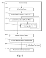
- FIG. 6 illustrates an alternative example process in which plurality of model diffraction patterns for different estimated target shapes (candidate structures) are calculated in advance and stored in a library for comparison with a real measurement.
- the underlying principles and terminology are the same as for the process of FIG. 5 .
- the steps of the FIG. 6 process are:
- step 602 the process of generating the library is performed.
- a separate library may be generated for each type of target structure.
- the library may be generated by a user of the measurement apparatus according to need, or may be pre-generated by a supplier of the apparatus.
- a ‘model recipe’ is established which defines a parameterized model of the target structure in terms of a number of parameters p i (p 1 , p 2 , p 3 and so on). Considerations are similar to those in step 503 of the iterative process.
- a first set of parameters p 1 (0) , p 2 (0) , p 3 (0) , etc. is generated, for example by generating random values of all the parameters, each within its expected range of values.
- a model diffraction pattern is calculated and stored in a library, representing the diffraction pattern expected from a target shape represented by the parameters.
- step 608 a new set of parameters p 1 (1) , p 2 (1) , p 3 (1) , etc. is generated. Steps 606 - 608 are repeated tens, hundreds or even thousands of times, until the library which comprises all the stored modeled diffraction patterns is judged sufficiently complete. Each stored pattern represents a sample point in the multi-dimensional parameter space. The samples in the library should populate the sample space with a sufficient density that any real diffraction pattern will be sufficiently closely represented.
- step 610 after the library is generated (though it could be before), the real target 30 is placed in the scatterometer and its diffraction pattern is measured.
- the measured pattern is compared with the modeled patterns stored in the library to find the best matching pattern.
- the comparison may be made with every sample in the library, or a more systematic searching strategy may be employed, to reduce computational burden.
- the estimated target shape used to generate the matching library pattern can be determined to be the approximate object structure.
- the shape parameters corresponding to the matching sample are output as the measured shape parameters.
- the matching process may be performed directly on the model diffraction signals, or it may be performed on substitute models which are optimized for fast evaluation.
- step 616 optionally, the nearest matching sample is used as a starting point, and a refinement process is used to obtain the final parameters for reporting.
- This refinement process may comprise an iterative process very similar to that shown in FIG. 5 , for example.
- refining step 616 is needed or not is a matter of choice for the implementer. If the library is very densely sampled, then iterative refinement may not be needed because a good match will always be found. On the other hand, such a library might be too large for practical use. A practical solution is thus to use a library search for a coarse set of parameters, followed by one or more iterations using the merit function to determine a more accurate set of parameters to report the parameters of the target substrate with a desired accuracy. Where additional iterations are performed, it would be an option to add the calculated diffraction patterns and associated refined parameter sets as new entries in the library.
- a library can be used initially which is based on a relatively small amount of computational effort, but which builds into a larger library using the computational effort of the refining step 616 .
- Whichever scheme is used a further refinement of the value of one or more of the reported variable parameters can also be obtained based upon the goodness of the matches of multiple candidate structures.
- the parameter values finally reported may be produced by interpolating between parameter values of two or more candidate structures, assuming both or all of those candidate structures have a high matching score.
- the computation time of this iterative process is largely determined by the forward diffraction model at steps 506 and 606 , i.e. the calculation of the estimated model diffraction pattern using a rigorous optical diffraction theory from the estimated target shape.
- RCWA is commonly used in the forward diffraction model, while the Differential Method, the Volume Integral Method (VIM), Finite-difference time-domain (FDTD), and Finite element method (FEM) have also been reported.
- VIP Volume Integral Method
- FDTD Finite-difference time-domain
- FEM Finite element method
- This vector field F is formulated using a so-called normal-vector field, a fictitious vector field that is perpendicular to the material interface.
- Algorithms to generate normal-vector fields have been proposed in [3,5], within the context of RCWA. Normal-vector fields have been used not only in combination with RCWA, but also in combination with the Differential Method.
- RCWA central processing unit
- the linear system that has to be solved for VIM is much larger compared to RCWA, but if it is solved in an iterative way, only the matrix-vector product is needed together with the storage of several vectors. Therefore, the memory usage is typically much lower than for RCWA.
- the potential bottleneck is the speed of the matrix-vector product itself. If the Li rules [10,11] were to be applied in VIM, then the matrix-vector product would be much slower, due to the presence of several inverse sub-matrices. Alternatively, the Li rules can be ignored and FFTs can be used to arrive at a fast matrix-vector product, but the problem of poor convergence remains.
- FIG. 7 illustrates schematically the scattering geometry that may be reconstructed in accordance with an embodiment of the present invention.
- a substrate 802 is the lower part of a medium layered in the z direction. Other layers 804 and 806 are shown.
- a two dimensional grating 808 that is periodic in x and y is shown on top of the layered medium. The x, y and z axes are also shown 810 .
- An incident field 812 interacts with and is scattered by the structure 802 to 808 resulting in a reflected field 814 .
- the structure is periodic in at least one direction, x, y, and includes materials of differing properties such as to cause a discontinuity at a material boundary between the differing materials in an electromagnetic field, E tot , that comprises a total of incident, E inc , and scattered, E ⁇ , electromagnetic field components.
- FIG. 8 shows the structure of the background and FIG. 9 schematically illustrates the Green's function that may be used to calculate the interaction of the incident field with the layered medium.
- the layered medium 802 to 806 corresponds to the same structure as in FIG. 7 .
- the x, y and z axes are also shown 810 along with the incident field 812 .
- a directly reflected field 902 is also shown.
- the point source (x′, y′, z′) 904 represents the Green's function interaction with the background that generates a field 906 . In this case because the point source 904 is above the top layer 806 there is only one background reflection 908 from the top interface of 806 with the surrounding medium. If the point source is within the layered medium then there will be background reflections in both up and down directions (not shown).
- the incident field E inc is a known function of angle of incidence, polarization and amplitude
- E tot is the total electric field that is unknown and for which the solution is calculated
- J c is the contrast current density
- G is the Green's function (a 3 ⁇ 3 matrix)
- ⁇ is the contrast function given by j ⁇ ( ⁇ (x,y,z) ⁇ b (z)), where ⁇ is the permittivity of the structure and ⁇ b is the permittivity of the background medium.
- ⁇ is zero outside the gratings.
- the Green's function G (x,x′,y,y′,z,z′) is known and computable for the layered medium including 802 to 806 .
- the Green's function shows a convolution and/or modal decomposition (m 1 , m 2 ) in the xy plane and the dominant computation burden along the z axis in G are convolutions.
- the total electric field is expanded in Bloch/Floquet modes in the xy plane.
- Multiplication with ⁇ becomes: (a) discrete convolution in the xy plane (2D FFT); and (b) product in z.
- the Green's function interaction in the xy plane is an interaction per mode.
- the Green's function interaction in z is a convolution that may be performed with one-dimensional (1D) FFTs with a complexity O(N log N).
- the number of modes in xy is M 1 M 2 and the number of samples in z is N.
- the efficient matrix-vector product has a complexity O(M 1 M 2 N log(M 1 M 2 N)) and the storage complexity is O(M 1 M 2 N).
- FIG. 10 is a flow chart of the high level method of solving the linear system corresponding to the VIM formula. This is a method of calculating electromagnetic scattering properties of a structure, by numerically solving a volume integral.
- the first step is pre-processing 1002 , including reading the input and preparing FFTs.
- the next step is to compute the solution 1004 .
- post-processing 1006 is performed in which reflection coefficients are computed.
- Step 1004 includes various steps also shown at the right hand side of FIG. 10 . These steps are computing the incident field 1008 , computing the Green's Functions 1010 , computing the update vectors 1012 , updating the solution and residual error (e.g., using BiCGstab) 1014 and testing to see if convergence is reached 1016 . If convergence is not reached control loops back to step 1012 that is the computation of the update vectors.
- FIG. 11 illustrates the steps in computing update vectors corresponding to step 1012 of FIG. 10 using the volume integral method as known in the prior art, which is a method of calculating electromagnetic scattering properties of a structure, by numerically solving a volume integral equation for an electric field, E.
- the integral representation describes the total electric field in terms of the incident field and contrast current density, where the latter interacts with the Green's function, viz
- e i ⁇ ( m 1 , m 2 , z ) e ⁇ ( m 1 , m 2 , z ) - ⁇ - ⁇ ⁇ ⁇ G _ _ ⁇ ( m 1 , m 2 , z , z ′ ) ⁇ j ⁇ ( m 1 , m 2 , z ′ ) ⁇ d z ′ ( 1.1 ) for m 1 ,m 2 ⁇ .
- G denotes the spectral Green's function of the background medium, which is planarly stratified in the z direction
- e(m 1 ,m 2 ,z) denotes a spectral component of total electric field E(x,y,z), written in a spectral base in the xy plane
- j(m 1 ,m 2 ,z) denotes a spectral component of the contrast current density J c (x,y,z), also written in a spectral base in the xy plane.
- J c denotes the contrast current density
- ⁇ is the angular frequency
- ⁇ (x,y,z) is the permittivity of the configuration
- ⁇ b (z) is the permittivity of the stratified background
- E denotes the total electric field, all written in a spatial basis.
- Step 1102 is reorganizing the vector in a four-dimensional (4D) array.
- the first dimension has three elements J x c , J y c and J z c .
- the second dimension has elements for all values of m 1 .
- the third dimension has elements for all values of m 2 .
- the fourth dimension has elements for each value of z.
- the 4D array stores the spectral (in the xy plane) representation of the contrast current density (J x c , J y c , J z c )(m 1 ,m 2 ,z). For each mode (i.e. for all sample points in z, at the same time), steps 1104 to 1112 are performed.
- Equation (1.1) The three dotted parallel arrows descending from beside step 1106 correspond to computing the integral term in Equation (1.1), which is the background interaction with the contrast current density. This is performed by a convolution of (J x c , J y c , J z c )(m 1 ,m 2 ,z) with the spatial (with respect to the z direction) Green's function, using a multiplication in the spectral domain (with respect to the z direction).
- step 1104 the spectral contrast current density (J x c , J y c , J z c )(m 1 ,m 2 ,z) is taken out as three 1D arrays for each of x, y, and z.
- step 1106 the convolution begins by computing the 1D FFT forward for each of the three arrays into the spectral domain with respect to the z direction to produce (J x c , J y c , J z c )(m 1 ,m 2 ,k z ), where k z is the Fourier variable with respect to the z direction.
- step 1108 the truncated Fourier transform of the contrast current density is multiplied in the spectral domain (with respect to the z direction) by the Fourier transform of the spatial Green's function g free .
- step 1110 a 1D FFT backwards is performed into the spatial domain with respect to the z direction.
- background reflections in the spatial domain with respect to z are added. This separation of the background reflections from the Green's function is a conventional technique and the step may be performed by adding rank-1 projections as will be appreciated by one skilled in the art.
- the update vectors for the scattered electric field, (E x , E y , E z )(m 2 , m 2 , z), thus calculated are placed back into the 4D array in step 1114 .
- steps 1116 to 1122 are performed.
- the three parallel dotted arrows descending from step 1114 in FIG. 11 correspond to the processing of three 2D arrays, one each for E x , E y and E z respectively, by steps 1116 to 1122 carried out for each sample point, z.
- step 1116 involves taking out the three 2D arrays (the two dimensions being for m 1 and m 2 ).
- step 1118 a 2D FFT is computed forward for each of the three arrays into the spatial domain.
- step 1120 each of the three arrays is multiplied by the spatial representation of the contrast function ⁇ (x,y,z) that is filtered by the truncation of the Fourier representation.
- the convolution is completed in step 1122 with the 2D FFT backwards into the spectral (in the xy plane) domain yielding the spectral contrast current density with respect to the scattered electric field (J x c,s , J y c,s , J z c,s )(m 1 ,m 2 ,z).
- step 1124 the calculated spectral contrast current density is placed back into the 4D array.
- the next step is reorganizing the 4D array in a vector 1126 , which is different from step 1102 “reorganizing the vector in a 4D array”, in that it is the reverse operation: each one-dimensional index is uniquely related to a four-dimensional index.
- step 1128 the vector output from step 1126 is subtracted from the input vector, corresponding to the subtraction in the right-hand side of Equation (1.1) multiplied by the contrast function ⁇ (x,y,z).
- the input vector is the vector that enters at step 1102 in FIG. 11 and contains (J x c , J y c , J z c )(m 1 ,m 2 ,z).
- a problem with the method described in FIG. 11 is that it leads to poor convergence. This poor convergence is caused by concurrent jumps in permittivity and contrast current density for the truncated Fourier-space representation.
- the Li inverse rule is not suitable for overcoming the convergence problem because in VIM the complexity of the inverse rule leads to a very large computational burden because of the very large number of inverse operations that are needed in the VIM numerical solution.
- Embodiments of the present invention overcome the convergence problems caused by concurrent jumps without resorting to use of the inverse rule as described by Li. By avoiding the inverse rule, embodiments of the present invention do not sacrifice the efficiency of the matrix-vector product that is required for solving the linear system in an iterative manner in the VIM approach.
- FIG. 12 illustrates an embodiment of the present invention. This involves numerically solving a volume integral equation for a contrast current density, J. This is performed by determining components of the contrast current density, J, by using a field-material interaction operator, M, to operate on a continuous component of the electromagnetic field, E S , and a continuous component of a scaled electromagnetic flux density, D S , corresponding to the electromagnetic field, E S , the scaled electromagnetic flux density, D S , being formed as a scaled sum of discontinuous components of the electromagnetic field, E S , and of the contrast current density J.
- M field-material interaction operator
- This embodiment employs the implicit construction of a vector field, F S , that is related to the electric field, E S , and a current density, J, by a selection of components of E and J, the vector field, F, being continuous at one or more material boundaries, so as to determine an approximate solution of a current density, J.
- the vector field, F is represented by at least one finite Fourier series with respect to at least one direction, x, y, and the step of numerically solving the volume integral equation comprises determining a component of a current density, J, by convolution of the vector field, F, with a field-material interaction operator, M.
- the field-material interaction operator, M comprises material and geometric properties of the structure in the at least one direction, x, y.
- the current density, J may be a contrast current density and is represented by at least one finite Fourier series with respect to the at least one direction, x, y.
- the continuous-component-extraction operators are convolution operators, P T and P n , acting on the electric field, E, and a current density, J.
- the convolutions are performed using a transformation such as one selected from a set comprising a fast Fourier transform (FFT) and number-theoretic transform (NTT).
- FFT fast Fourier transform
- NTT number-theoretic transform
- the convolution operator, M operates according to a finite discrete convolution, so as to produce a finite result.
- the structure is periodic in at least one direction and the continuous component of the electromagnetic field, the continuous component of the scaled electromagnetic flux density, the components of the contrast current density and the field-material interaction operator are represented in the spectral domain by at least one respective finite Fourier series with respect to the at least one direction and the method further comprises determining coefficients of the field-material interaction operator by computation of Fourier coefficients.
- the methods described herein are also relevant for expansions based on continuous functions other than those of the Fourier domain, e.g. for expansion in terms of Chebyshev polynomials, as a representative of the general class of pseudo-spectral methods, or for expansions on a Gabor basis.
- FIG. 12 shows the step 1202 of solving the VIM system for a current density, J, by employing an intermediate vector field, F, formed using continuous-component-extraction operators, with a post-processing step 1204 to obtain a total electric field, E, by letting the Green's function operator act on a current density, J.
- FIG. 12 also shows at the right hand side a schematic illustration of performing an efficient matrix-vector product 1206 to 1220 to solve the VIM system iteratively. This starts with a current density, J, in step 1206 . The first time that J is set up, it can be started from zero. After that initial step, the estimates of J are guided by the iterative solver and the residual.
- step 1208 the convolutions and rank-1 projections between the Green's function, G, and the contrast current density, J, are computed to yield the scattered electric field, E S .
- intermediate vector field, F is computed in step 1214 using a convolution with two continuous-component-extraction operators P T and P n acting on the scattered electric field, E S , and the current density, J.
- P T the first continuous-component-extraction operator
- P n is used to extract the continuous component of the scaled electromagnetic flux density, D S , in step 1212 .
- step 1216 the field-material interaction operator (M) operates on the extracted continuous components.
- Step 1214 represents forming a vector field, F S , that is continuous at the material boundary from the continuous component of the electromagnetic field obtained in step 1210 and the continuous component of the scaled electromagnetic flux density obtained in step 1212 .
- the step of determining components of the contrast current density 1216 is performed by using a field-material interaction operator M to operate on the vector field, F S .
- Steps 1210 to 1216 are performed for each sample point in z with the convolutions being performed via FFTs.
- the convolution may be performed using a transformation such as one selected from a set comprising a fast Fourier transform (FFT) and number-theoretic transform (NTT).
- FFT fast Fourier transform
- NTT number-theoretic transform
- Operation 1218 subtracts the two computed results J S from J to obtain an approximation of J inc in 1220 , related to the incident electric field E inc . Because steps 1206 to 1220 produce update vectors then the post-processing step 1204 is used to produce the final value of the total electric field, E.
- the sum of all the update vectors may be recorded at step 1208 in order to calculate the scattered electric field, E S and the post processing step becomes merely adding the incident electric field, E inc , to the scattered electric field.
- that approach increases the storage requirements of the method, whereas the post-processing step 1204 is not costly in storage or processing time, compared to the iterative steps 1206 to 1220 .
- FIG. 13 a is a flow chart of the computation of update vectors in accordance with an embodiment of present invention.
- the flow chart of FIG. 13 corresponds to the right hand side (steps 1206 to 1220 ) of FIG. 12 .
- step 1302 the vector is reorganized in a 4D array.
- step 1304 three 2D arrays are taken out of the 4D array.
- These three 2D arrays (E x , E y , E z )(m 1 , m 2 , z) correspond to the Cartesian components of the scattered electric field, E, each having the 2 dimensions corresponding to m 1 and m 2 .
- step 1306 the convolution of the continuous vector field, represented by (F x , F y , F z )(m 1 , m 2 , z) begins with the computation in step 1306 of the 2D FFT forward into the spatial domain for each of the three arrays, represented by (E x , E y , E z )(m 1 , m 2 , z).
- step 1308 the Fourier transform (E x , E y , E z )(x, y, z) obtained from step 1306 is multiplied in the spatial domain by the spatial multiplication operator MP T (x, y, z), which has two functions: first it filters out the continuous components of the scattered electric field by applying the tangential projection operator P T , thus yielding the tangential components of the continuous vector field, F, and second it performs the multiplication by the contrast function M, which relates the continuous vector field F to the contrast current density J, regarding only the scattered fields.
- MP T x, y, z
- the scattered electric field, (E x , E y , E z )(m 2 , m 2 , z), placed in the 4D array at step 1114 is fed into both step 1304 , as discussed above, and step 1310 , as discussed below.
- step 1310 for each sample point in z (that is, for each layer) a scaled version of the scattered electric flux density, D, is formed as the scaled sum of the scattered electric field, obtained from step 1114 , and the contrast current density, fed forward from step 1302 , after which three 2D arrays are taken out, corresponding to the Cartesian components of D in the spectral domain.
- step 1312 the 2D FFT of these arrays are performed, yielding the Cartesian components (D x , D y , D z )(x, y, z) in the spatial domain.
- step 1314 these arrays are multiplied in the spatial domain by the multiplication operator, MP n , which has two functions: first the normal component of the scaled flux density, which is continuous, is filtered out and yields the normal component of the continuous vector field, F , and second it performs the multiplication by the contrast function M, which relates the continuous vector field F to the contrast current density J, regarding only the scattered fields.
- MP n the multiplication operator
- MF is transformed in step 1318 by a 2D FFT backwards into the spectral domain to yield the approximation of the spectral contrast current density, represented by M F (m 1 , m 2 , z).
- M F the spectral contrast current density related to the scattered field
- step 1320 the resulting spectral contrast current density related to the scattered field, is placed back in the 4D array and subsequently transformed back to a vector in step 1322 .
- step 1324 the calculation of the approximation of the known contrast current density related to the incident electric field, J inc , is completed with the subtraction of the result of step 1322 from the total contrast current density fed forward from the input of step 1302 .
- the vector field, F is formed 1404 from a combination of field components of the electromagnetic field, E, and a corresponding electromagnetic flux density, D, by using a normal-vector field, n, to filter out continuous components of the electromagnetic field, E, tangential to the at least one material boundary, E T , and also to filter out the continuous components of the electromagnetic flux density, D, normal to the at least one material boundary, D n .
- the continuous components of the electromagnetic field, E T are extracted using a first continuous-component-extraction operator, P T .
- the continuous component of the scaled electromagnetic flux density, D n is extracted using a second continuous-component-extraction operator, P n .
- the scaled electromagnetic flux density, D is formed as a scaled sum of discontinuous components of the electromagnetic field, E, and of the contrast current density, J.
- the normal-vector field, n is generated 1402 in a region of the structure defined with reference to the material boundaries, as described herein.
- the region extends to or across the respective boundary.
- the step of generating the localized normal-vector field may comprise decomposing the region into a plurality of sub-regions, each sub-region being an elementary shape selected to have a respective normal-vector field with possibly a corresponding closed-form integral.
- These sub-region normal-vector fields are typically predefined. They can alternatively be defined on-the-fly, but that requires additional processing and therefore extra time.
- the sub-region normal-vector field may be predefined to allow numerical integration by programming a function that gives the (Cartesian) components of the normal-vector field as output, as a function of the position in the sub-region (as input). This function may then be called by a quadrature subroutine to perform the numerical integration. This quadrature rule can be arranged in such a way that all Fourier components are computed with the same sample points (positions in the sub-region), to further reduce computation time.
- a localized integration of the normal-vector field over the region is performed 1406 to determine coefficients of the field-material interaction operator, which is in this embodiment the convolution-and change-of-basis operator, C (C ⁇ in Equation (4)).
- the material convolution operator, M (j ⁇ [ ⁇ C ⁇ ⁇ b C ⁇ ] defined in Equations (4) and (5)), is also constructed using this localized normal-vector field.
- the step of performing the localized integration may comprise using the respective predefined normal-vector field for integrating over each of the sub-regions.
- Components of the contrast current density (J x c,s , J y c,s , J z c,s ), are numerically determined 1408 by using the field-material interaction operator, M, to operate on the vector field, F, and thus on the extracted continuous components of the electromagnetic field, E T , and continuous component of the scaled electromagnetic flux density D n .
- the electromagnetic scattering properties of the structure can therefore be calculated 1410 using the determined components of the contrast current density, (J x c,s , J y c,s , J z c,s ), in this embodiment by solving a volume integral equation for the contrast current density, J c , so as to determine an approximate solution of the contrast current density.
- the region may correspond to the support of the contrast source.
- the step of generating the localized normal-vector field may comprise scaling at least one of the continuous components.
- the step of scaling may comprise using a scaling function ( ⁇ ) that is continuous at the material boundary.
- the scaling function may be constant.
- the scaling function may be equal to the inverse of a background permittivity.
- the step of scaling may further comprise using a scaling operator (S) that is continuous at the material boundary, to account for anisotropic material properties.
- S scaling operator
- the scaling function may be non-zero.
- the scaling function may be constant.
- the scaling function may be equal to the inverse of a background permittivity.
- the scaling may be configured to make the continuous components of the electromagnetic field and the continuous components of the electromagnetic flux density indistinguishable outside the region.
- the step of generating the localized normal-vector field may comprise using a transformation operator (T n ) directly on the vector field to transform the vector field from a basis dependent on the normal-vector field to a basis independent of the normal-vector field.
- T n transformation operator
- the basis independent of the normal-vector field may be the basis of the electromagnetic field and the electromagnetic flux density.
- a spectral-domain volume-integral equation for the electric field may be used to compute the reflection coefficients.
- the key point in a continuous-vector-field VIM approach is to express the electric field E and the contrast current density J in terms of an auxiliary field F.
- the former step is based on the integral representation for the scattered electric field, the relation between the electric field and the electric flux density on the one hand and the contrast current density on the other, and the projection operators P n and P T .
- the corresponding matrix-vector product for the contrast current density is shown in FIG. 13 b.
- the operators MP T and MP n can be implemented as shown in FIG. 13 c.
- An embodiment of the present invention provides a localized normal-vector field. This enables a cut-and-connect technique with basic building blocks that allows for a rapid and flexible generation of a normal-vector field for more complicated shapes. Embodiments of the present invention address the above issues regarding setup time and continuity under parameter changes mentioned above, by employing parameterized building blocks with normal-vector fields that vary continuously as a function of the parameters, such as varying dimensions of a grating structure during iterative reconstruction.
- n x and n y be the x and y components of the normal-vector field
- the vector field t 2 is generated via the cross product between n and t 1 .
- the projection operators P T and P n have some other useful properties.
- P T I ⁇ P n , where I is the identity operator. This property shows that the normal-vector field itself is sufficient to generate both the operator P n and the operator P T , which was already observed from the construction of the tangential-vector fields.
- the first improvement that we introduce to the concept of the normal-vector field formalism [1] is the possibility to scale the components of the vector field F.
- ⁇ is a non-zero scaling function, which is continuous across material interfaces.
- the consequences of this scaling are two-fold. First, it can bring the scale of the components of the vector field F to the same order of magnitude. This will improve the conditioning of the linear systems C ⁇ and ⁇ C ⁇ . Second, and more importantly, it has far-reaching consequences for the locality of the normal-vector field n, as will be demonstrated below. In fact, the second aspect is so important that it will usually guide the choices for scaling, even if it results in a sub-optimal conditioning.
- P T ⁇ D P T ⁇ M ⁇ ⁇ P T ⁇ F + P T ⁇ M ⁇ ⁇ ( P n ⁇ M ⁇ ⁇ P n ) - 1 ⁇ ( 1 ⁇ ⁇ P n - P n ⁇ M ⁇ ⁇ P T ) ⁇ F .
- ⁇ F ⁇ [ 1 ⁇ ⁇ P n + P T ⁇ M ⁇ ⁇ C ⁇ ] ⁇ F .
- the support of the latter operator determines the domain over which the normal-vector field n is required to generate the coefficients of the operators C ⁇ and ⁇ C ⁇ .
- LER line-edge roughness
- line-width roughness LER
- LER line-edge roughness
- This rigorous modeling approach is usually very time consuming. Therefore, LER is typically modeled via an effective medium approximation, in which a transition layer captures the part of the line that contains the roughness. This transition layer is best modeled as an anisotropic medium.
- the directions of anisotropy generally depend on the geometrical features of the roughness, see e.g. [12]. Since a line is automatically aligned with the Cartesian coordinate system, boundary-conforming anisotropy is automatically equal to anisotropy along the coordinate axes.
- anisotropy is defined independent of the scattering geometry.
- edge roughness anisotropic effective-medium models are known for lines but not for other geometrical shapes, e.g. contact holes with a circular or elliptical cross section.
- Embodiments of the present invention employ normal-vector fields to arrive at better numerical convergence.
- Embodiments may have the ability to model bi-refringent media with respect to the horizontal and vertical directions. It is possible to handle more general anisotropic media in which the directions of anisotropy are pointing along the boundary and normal to the boundary of a pattern, i.e. the anisotropy is boundary-conforming.
- anisotropy is boundary-conforming.
- such types of anisotropy provide a natural extension to effective-medium approaches, which are e.g. used to model LER.
- no additional processing is required, since the normal of each boundary is already determined within the normal-vector field approach used as described herein.
- the flux density D and the field strength E on the one hand can be related to the auxiliary field F on the other.
- the electromagnetic flux density is related to the electric field using, in the region in which the localized normal vector field is generated and local to the material boundary, a component of permittivity ⁇ n normal to the material boundary and at least one other, different, component ⁇ t , ⁇ z of permittivity tangential to the material boundary
- This embodiment widens the range of effective-medium approaches, e.g. for edge roughness on curved boundaries. Moreover, no extra processing is required to set up this model since all ingredients are available. Hence no extra time is spent in setting up the corresponding mathematical and numerical problem.
- boundary-conforming anisotropy is a suitable way of dealing with edge roughness, it leads to significant speed-up of a CD reconstruction process involving edge roughness.
- the normal-vector field has the potential to be localized by choosing a proper scaling between the components of the vector field F.
- the tangential-vector fields and normal-vector field are not representative for the components of the solver.
- a Cartesian basis is more suitable, e.g., within VIM, RCWA, or the Differential Method. Since a projection operator does not change the basis of the vector field, an additional transformation of the electric field and the electric flux density may be required, to arrive at the required basis for the Maxwell solver.
- the permittivity operator M ⁇ which is typically expressed in terms of Cartesian coordinates.
- the operator M ⁇ must be transformed too.
- the operator M ⁇ also contains the operator M ⁇ .
- M ⁇ is a scalar multiplication, its final form is independent of the chosen basis.
- the definition of the projection operator P n as given in Eq. (6) is independent of the chosen basis, although its actual matrix representation does depend on the chosen basis for the normal vector field. Therefore, we choose to write P n as a basis-independent operator.
- T n transforms a vector field expressed in terms of the normal and tangential basis into e.g., Cartesian vector fields that are used for the electric field, the electric flux density, and the permittivity operator M ⁇ . Then we can write for the electric field, expressed in Cartesian coordinates
- a second important class of problems is the case in which the grating material(s) have birefringent material properties, where the axis of anisotropy is the z-axis, i.e.
- ⁇ T and ⁇ N are, in principle, functions of x, y, and z.
- the normal-vector field problem in the xy plane is again an isotropic problem and the considerations for the scaling parameter ⁇ are now quite similar to those in Section 2.5, e.g., for a two-media problem one should scale the electric flux density with respect to ⁇ T of the interior or exterior of the object, such that the scaled electric flux density becomes identical to the electric field in a dedicated part of the unit cell.
- the grating For more general grating geometries, one can apply a staircase approximation of the grating, with respect to the z direction. Then, the grating consists of a sequence of binary gratings and for each of these binary gratings the strategy outlined above can be followed.
- b 1 2 ⁇ ⁇ ( a 1 ⁇ x ⁇ a 2 ⁇ y - a 1 ⁇ y ⁇ a 2 ⁇ x ) ⁇ ( a 2 ⁇ y - a 2 ⁇ x 0 )
- b 2 2 ⁇ ⁇ ( a 1 ⁇ x ⁇ a 2 ⁇ y - a 1 ⁇ y ⁇ a 2 ⁇ x ) ⁇ ( - a 1 ⁇ y a 1 ⁇ x 0 ) , ( 59 )
- the diagonal elements contain the Fourier integral of unity over the unit cell and the Fourier integral of the product of normal-vector components and a position-dependent function of the scaling factor ⁇ (x, y, z) and the permittivity ⁇ (x, y, z).
- the first integral i.e. the integral of unity over the unit cell, is equal to ⁇ m 1 ,0 ⁇ m 2 ,0 .
- the second integral can be substantially simplified for the case of an isotropic medium when the scaling factor ⁇ is chosen equal to 1/ ⁇ b . This function is then zero outside and constant inside the support of the contrast source.
- the Fourier coefficients c ij (m 1 , m 2 , z) can now be expressed in terms of the integral
- ⁇ ij ⁇ ( m 1 , m 2 , z ) 1 ( a 1 ⁇ x ⁇ a 2 ⁇ y - a 1 ⁇ y ⁇ a 2 ⁇ x ) ⁇ ⁇ ⁇ support ⁇ n i ⁇ ( x , y , z ) ⁇ n j ⁇ ( x , y , z ) ⁇ e i ⁇ [ b ex ⁇ ( m 1 , m 2 ) ⁇ x + b ey ⁇ ( m 1 , m 2 ) ⁇ y ] ⁇ d x ⁇ d y . ( 66 )
- c ij ⁇ ( m 1 , m 2 , z ) ⁇ ij ⁇ ⁇ m 1 , 0 ⁇ ⁇ m 2 , 0 + ( ⁇ b ⁇ r - 1 ) ⁇ ⁇ ij ⁇ ( m 1 , m 2 , z ) , ( 67 )
- the computation of the ⁇ ij integral can be further simplified by transforming to the local coordinate system.
- FIG. 15 a is a definition of global (x, y) and local (x′′, y′′) coordinate systems for the rotated ellipse with offset c 0 .
- the NV field of the scattering object is only affected by rotation.
- the product of NV components in Eq. (66) in the global (x, y)- and local (x′′, y′′)-system are related by a linear transformation
- M nn′′ is the coupling matrix from Eq. (73)
- ⁇ ij ′′ ⁇ ( m 1 , m 2 ) e i ⁇ [ b c , c 0 ] ( a 1 ⁇ x ⁇ a 2 ⁇ y - a 1 ⁇ y ⁇ a 2 ⁇ x ) ⁇ ⁇ ⁇ support ⁇ n i ′′ ⁇ n j ′′ ⁇ e i ⁇ ( k ex ⁇ ( m 1 , m 2 ) ⁇ x ′′ + k ey ⁇ ( m 1 , m 2 ) ⁇ y ′′ ) ⁇ d x ′′ ⁇ d y ′′ , ( 75 )
- the ⁇ ′′ ij integral is still computed over an area that is equal to the support of the contrast source (translation and rotation do not change that), but in the local coordinate system the integral is more easily evaluated—as we shall see—for the ellipse and the rectangle.
- FIG. 15 b illustrates a NV field for the elliptical coordinate system and FIG. 15 c illustrates conformal mapping.
- the elliptic coordinate system has the advantage that an analytical expression for ⁇ ′′ ij can be derived and that the normal-vector field only has a singularity at (0,0) while the conformal mapping has singular behavior over the line connecting the foci.
- the normal-vector field can be derived as the vector perpendicular to the tangential vector ⁇ r/ ⁇
- n 1 e 2 ⁇ cos 2 ⁇ ⁇ + sin 2 ⁇ ⁇ ⁇ ( e ⁇ ⁇ cos ⁇ ⁇ ⁇ sin ⁇ ⁇ ⁇ ) . ( 79 )
- ⁇ ij ′′ ⁇ ( m 1 , m 2 ) e i ⁇ [ b e ⁇ c 0 ] ( a 1 ⁇ x ⁇ a 2 ⁇ y - a 1 ⁇ y ⁇ a 2 ⁇ x ) ⁇ ⁇ 0 a ⁇ ⁇ 0 2 ⁇ ⁇ ⁇ n i ⁇ ( ⁇ ) ⁇ n j ⁇ ( ⁇ ) ⁇ e i ( k ex ⁇ ( m 1 , m 2 ) ⁇ rcos ⁇ ⁇ ⁇ + ek ey ⁇ ( m 1 , m 2 ) ⁇ rsin ⁇ ⁇ ⁇ ] ⁇ er ⁇ d r ⁇ d ⁇ , ( 81 )
- N b is the number of terms that is retained in the summation over the even
- FIG. 16 a illustrates a corresponding continuous NV field for the rectangle.
- This expression does not lend itself for deriving an analytical expression of the ⁇ ij integral.
- FIG. 16 b illustrates a corresponding discontinuous NV field for the rectangle. This normal-vector field is constant for each triangle which makes the ⁇ ′′ ij integral particularly simple to calculate.
- ⁇ ij ′′ ⁇ ( m 1 , m 2 ) e i ⁇ ( b e ⁇ c 0 ) ( a 1 ⁇ x ⁇ a 2 ⁇ y - a 1 ⁇ y ⁇ a 2 ⁇ x ) ⁇ n i ⁇ n j ⁇ ⁇ ⁇ 1 ⁇ ⁇ 2 ⁇ ⁇ ⁇ 3 ⁇ ⁇ 4 ⁇ e i ⁇ ( k ex ⁇ ( m 1 , m 2 ) ⁇ x + k ey ⁇ ( m 1 , m 2 ) ⁇ y ) ⁇ d x ⁇ d y . ( 92 )
- triangle ⁇ 2 we only need to swap r a r b and k ex k ey .
- the result for triangles ⁇ 3 and ⁇ 4 is simply the complex conjugate of the integral for resp. ⁇ 1 and ⁇ 2 .
- the previous section on the NV field generation for the rectangle shows a very powerful method for generating the NV field for more arbitrary shapes.
- These shapes can be decomposed in elementary shapes for which the ⁇ ij integral has a closed form suited for fast computation. By summing up the relevant ⁇ ij integrals for each elementary shape at a particular Fourier mode index, the spectral representation of C ⁇ and ⁇ C ⁇ can be easily obtained.
- the class of elementary shapes must be large enough to generate all relevant more complex shapes.
- the class of elementary shapes comprises: (A) triangles with a constant NV field: if one interface is a material interface, the NV field must be perpendicular to this interface.
- the NV field can be chosen arbitrarily; (B) trapezoids with a constant NV field (the rectangle is a special case): if one interface is a material interface, the NV field must be perpendicular to this interface. If there is no material interface, the NV field can be chosen arbitrarily; or (C) circle segment with a radial NV field and material interface along the circle edge.
- FIG. 17 illustrates meshing a ‘dogbone’ in these elementary shapes.
- FIG. 18 illustrates building the normal-vector field of a prism with a cross section of a rounded rectangle from smaller rectangles 1802 and circle segments 1804 in accordance with an embodiment of the present invention. Note that the normal-vector field shown by the arrows is perpendicular to the physical interfaces at those physical interfaces.
- a method to construct a normal-vector field locally i.e. over the scattering object or parts thereof
- a cut-and-paste meshing technique where the normal-vector field of an arbitrary shape is composed of the normal-vector fields of two or more elementary shapes selected from: a prism with the following cross section: a triangle; a rectangle; a trapezoid; or a circular segment; a tetrahedron; a bar; a hexahedron with two parallel faces; an apex truncated pyramid with truncation face parallel to the ground plane; and spherical segment.
- the normal-vector field can be very simply and rapidly generated.
- an embodiment of the present invention breaks up the Fourier integrals into several integrals over the support of the various media in the computational domain. For each of these domains, dedicated quadrature rules are applied in combination with an interpolation algorithm to generate the normal-vector field on this domain. Interpolation is applied based on basis functions with periodic continuation, to avoid artificial discontinuities in the integrants, due to a particular choice for the boundaries of unit cell. Further, it is possible to further limit the support of the normal-vector field to a direct neighborhood of a material interface. This leads to an even more parsimonious approach to generate normal-vector fields for more complicated shapes.
- FIG. 19 illustrates rotated and shifted triangle with NV field and local coordinate system.
- FIG. 19 shows an arbitrary triangle with vertices A, B and C.
- the vertex opposite to the material interface, (B ⁇ C) is chosen as the local origin. Note that the vertices are ordered in a counterclockwise direction.
- ⁇ 0 we rotate over angle ⁇ 0 to get to the local coordinate system.
- B′′ and C′′ are given by Eq. (72)
- FIG. 20 illustrates a rotated and shifted trapezoid with NV field and local coordinate system.
- the circle segment is defined as a section from a circle with origin A, lower radius endpoint B and section angle ⁇ s .
- FIG. 21 illustrates rotated and shifted circle segment with NV field and local coordinate system.
- the NV component ⁇ ′′ ij can be computed along the same lines as for the full ellipse in Section 3.3.
- the main difference is that the angular integrals are now evaluated from 0 to an arbitrary angle ⁇ s . This has the effect that the angular integral over the odd terms in the Bessel summation ⁇ ij o (k,0, ⁇ s ) ⁇ 0. Also for the odd terms, the radial integral over the Bessel function has an analytical expression (see Appendix A)
- Standard scattered-data interpolation algorithms use so-called radial basis functions, i.e. basis functions that only depend on the distance between a data point and the interpolation point.
- radial basis functions i.e. basis functions that only depend on the distance between a data point and the interpolation point.
- this is usually a good idea, since it allows nearby data to have a higher impact on the interpolated data as compared to data far away.
- the distance between a data point and an interpolation point also becomes periodic. If we do not take this into account, the interpolation across a periodic boundary can introduce artificial discontinuities, which may deteriorate the convergence of certain quadrature rules or even the convergence of the solution of the electromagnetic fields projected on the normal-vector field. Therefore, we look for alternatives for the scattered-data interpolation with radial basis functions.
- the key idea is to generate a periodic-distance function that exhibits the periodicity of the configuration and to let this function replace the distance function.
- d p ⁇ ( x , x ′ ) ⁇ sin ⁇ ( 2 ⁇ ⁇ ⁇ x - x ′ p ) ⁇ ( 109 ) also satisfies the basic criteria for a distance measure d(x, x′), i.e.
- d ⁇ ⁇ ( r , r ′ ) f ⁇ ( ⁇ 1 - ⁇ 1 ) 2 ⁇ ⁇ a 1 ⁇ 2 + f ⁇ ( ⁇ 2 - ⁇ 2 ) 2 ⁇ ⁇ a 2 ⁇ 2 + 2 ⁇ f ⁇ ( ⁇ 1 - ⁇ 1 ) ⁇ f ⁇ ( ⁇ 2 - ⁇ 2 ) ⁇ ( a 1 , a 2 ) + ( z - z ′ ) 2 , ( 113 )
- ⁇ (x) is for example equal to x mod 1 or sin( ⁇ x).
- the normal-vector field is not required, provided the basis of the vector field F is independent of the normal-vector field, e.g., it is expressed in Cartesian coordinates.
- Another choice for S is to use a smoothed version of the permittivity distribution. For this choice, the region where the normal-vector field is required is shrunk even further.
- the main merits of the localized normal-vector field i.e. the possibility to pre-compute expressions of the coefficients for the operators C ⁇ and ⁇ C ⁇ for each object separately and the possibility to apply the cut-and-connect strategy, are still valid in the general anisotropic case.
- the coefficients of the operators are typically more complicated, since the directions of anisotropy mixes with the direction on the normal-vector field. This can for example be observed from the operator (P n M ⁇ P n ) ⁇ 1 , which was independent of the normal-vector field for isotropic media, whereas it does depend on the normal-vector field and the direction of the anisotropy in the general case.
- Embodiments of the present invention allow for a faster and more flexible setup of normal-vector fields in 2D and 3D, which results in faster CD reconstruction times and faster library recipe generation. For a simple example, we have observed speed up from several minutes to sub-seconds on the same computing hardware.
- E inc E ⁇ GJ (2.69)
- F P T E+P n ( ⁇ b E+J/j ⁇ ) (2.70)
- J j ⁇ ( ⁇ C ⁇ ⁇ b ⁇ C ⁇ )
- F MF (2.71)
- E inc denotes the incident field
- G denotes the matrix representation of the Green's function of the stratified background medium
- M P T , P n , C ⁇ and ( ⁇ C ⁇ ) correspond to efficient matrix-vector products in the form of FFTs.
- Lalanne [13] proposed a weighted-average formula for the permittivity matrix M ⁇ (denoted in [13] as E) and the inverse matrix of the inverse-permittivity matrix (M inv( ⁇ ) ) ⁇ 1 (denoted in [13] as P ⁇ 1 ).
- E permittivity matrix
- M inv( ⁇ ) ) ⁇ 1 inverse-permittivity matrix
- P ⁇ 1 ⁇ 1
- Eqs (2.73) and (2.74) can be implemented as a larger linear system in the form of Eq. (2.72).
- the first set of equations, involving the operators I and G remains untouched.
- the last set of equations, involving C 31 , C 32 , C 33 , and the last row of the right-hand side would be absent.
- This may be implemented in calculating electromagnetic scattering properties of a structure, by including numerically solving a volume integral equation for the current density, J, and the vector field, F, that is related to and different from said electromagnetic field, E, so as to determine an approximate solution of the current density, J.
- the vector field, F is related to the electric field, E, by the invertible operator M inv( ⁇ ) .
- Li [10,11] has shown that the field-material interaction is better captured in a spectral basis when the corresponding interaction matrix is composed of sums of products of (block) Toeplitz and inverse (block) Toeplitz matrices.
- the (block) Toeplitz matrices are usually referred to as a representation of the “Laurent rule”, which corresponds to a standard discrete convolution.
- the inverse (block) Toeplitz matrices are usually referred to as the “inverse rule”.
- the inverse rule should be applied whenever a field component is discontinuous across a material interface and the Laurent rule is applied when the field component is continuous across a material interface. These rules are often referred to as the “Li rules”.
- the (block) Toeplitz matrices allow for efficient matrix-vector products in the form of FFTs, but the inverse Toeplitz matrices do not have the Toeplitz form and therefore a fast matrix-vector product is not easily formed. Therefore, by extending the idea of auxiliary vector fields, we can introduce additional auxiliary fields together with constraints, to arrive at an efficient matrix-vector product that also takes into account the inverse of (block) Toeplitz matrices.
- ⁇ i x D x is factorizable in Fourier space, but ⁇ j y D x is not, as D x has a discontinuity in the y direction at a material interface. Since the functions ⁇ ⁇ ⁇ can be interpreted as projection operators, we can employ the following.
- the functions ⁇ o and ⁇ e can be constructed as continuous functions, e.g. via linear interpolation on segments outside the support of the even and odd projection operators.
- FIG. 22 illustrates a procedure to approximate an ellipse 2202 by a staircased approximation 2204 in the transverse plane by introducing odd 2206 (white support) and even 2208 (solid/shaded support) projection operators per dimension.
- odd 2206 white support
- even 2208 solid/shaded support
- ⁇ ⁇ 1 ⁇ b ⁇ 1 [1+ ⁇ oo ( x,y ) ⁇ o x ( x ) ⁇ o y ( y )+ ⁇ oe ( x,y ) ⁇ o x ( x ) ⁇ e y ( y )+ ⁇ eo ( x,y ) ⁇ e x ( x ) ⁇ o y ( y )+ ⁇ ee ( x,y ) ⁇ e x ( x ) ⁇ e y ( y )]. (2.86) which shows that there are only four two-dimensional projection operators (colors) involved.
- J x - j ⁇ ⁇ ⁇ ⁇ 1 , 1 ⁇ ⁇ 1 x ⁇ ( x ) ⁇ ⁇ J x j ⁇ + ⁇ b ⁇ ⁇ 1 y ⁇ ( y ) ⁇ [ E x inc + ( GJ ) x ] ⁇ , ( 2.98 ) which can be rewritten as the x-component of an integral equation, i.e.
- An advantage of embodiments of the present invention is that they allow for a contrast-source inversion (CSI) algorithm for reconstructing the grating profile in a metrology application.
- CSI contrast-source inversion
- Embodiments of the present invention avoid discontinuous operators operating on discontinuous vector fields and the associated performance penalties, thus providing improved convergence accuracy and speed.
- FIG. 23 shows in schematic form a computer system configured with programs and data in order to execute a method in accordance with an embodiment to the present invention.
- the computer system comprises a central processing unit (CPU) 2302 and random access memory (RAM) 2304 which is used to store the program instructions 2306 and data 2308 during execution of the program.
- the computer system also includes disk storage 2310 that is used to store program instructions and data before and after the execution of the program.
- the program instructions 2306 include Fast Fourier Transform routines 2312 , matrix multiplication functions 2314 , other arithmetic functions such as addition and subtraction 2316 and array organizing functions 2318 .
- the data 2308 comprises the 4D array 2320 and 2D arrays 2322 used during calculation of the solution of the VIM system. Other conventional computer components for input and output are not shown.
- a Fourier series expansion can be used to analyze aperiodic structures by employing perfectly matched layers (PMLs), or other types of absorbing boundary conditions to mimic radiation towards infinity, near the boundary of the unit cell on which the Fourier expansions are used.
- PMLs perfectly matched layers
- Embodiments of the present invention may be implemented in accordance with the reconstruction methods described with reference to FIGS. 5 and 6 to provide a method of reconstructing an approximate structure of an object from a detected electromagnetic scattering property arising from illumination of the object by radiation.
- Embodiments of the present invention may be implemented by implementing the methods described herein on the processing units PU described with reference to FIGS. 3 and 4 to provide an inspection apparatus for reconstructing an approximate structure of an object.
- the processors described with reference to FIGS. 3 , 4 and 23 may operate under the control of computer programs containing one or more sequences of machine-readable instructions for calculating electromagnetic scattering properties of a structure, the instructions being adapted to cause one or more processors to perform the methods described herein.
- any use of the terms “wafer” or “die” herein may be considered as synonymous with the more general terms “substrate” or “target portion”, respectively.
- the substrate referred to herein may be processed, before or after exposure, in for example a track (a tool that typically applies a layer of resist to a substrate and develops the exposed resist), a metrology tool and/or an inspection tool.
- the disclosure herein may be applied to such and other substrate processing tools.
- the substrate may be processed more than once, for example in order to create a multi-layer IC, so that the term substrate used herein may also refer to a substrate that already contains multiple processed layers.
- the methods according to embodiments of the present invention described above may be incorporated into the forward diffraction model for reconstructing an approximate structure of an object (not limited to 1D-periodic) from a detected electromagnetic scattering property, such as a diffraction pattern, arising from illumination of the object by radiation, as described above with reference to FIGS. 5 and 6 .
- the processing unit PU described above with reference to FIGS. 3 and 4 may be configured to reconstruct an approximate structure of an object using this method.
- imprint lithography a topography in a patterning device defines the pattern created on a substrate.
- the topography of the patterning device may be pressed into a layer of resist supplied to the substrate whereupon the resist is cured by applying electromagnetic radiation, heat, pressure or a combination thereof.
- the patterning device is moved out of the resist leaving a pattern in it after the resist is cured.
- UV radiation e.g., having a wavelength of or about 365, 355, 248, 193, 157 or 126 nm
- EUV radiation e.g., having a wavelength in the range of 5-20 nm
- particle beams such as ion beams or electron beams.
- lens may refer to any one or combination of various types of optical components, including refractive, reflective, magnetic, electromagnetic and electrostatic optical components.
- Electromagnetic encompasses electric and magnetic.
- electromagnetic scattering properties encompasses reflection and transmission coefficients and scatterometry measurement parameters including spectra (such as intensity as a function of wavelength), diffraction patterns (intensity as a function of position/angle) and the relative intensity of transverse magnetic- and transverse electric-polarized light and/or the phase difference between the transverse magnetic- and transverse electric-polarized light. Diffraction patterns themselves may be calculated for example using reflection coefficients.
- the invention may take the form of a computer program containing one or more sequences of machine-readable instructions describing a method as disclosed above, or a data storage medium (e.g., semiconductor memory, magnetic or optical disk) having such a computer program stored therein.
- a data storage medium e.g., semiconductor memory, magnetic or optical disk
Abstract
Description
-
- Gauss-Newton minimization of the difference between measured data and data computed from the estimated scattering setup;
- parameterized shapes in the scattering setup, e.g. radius and height of a contact hole;
- sufficiently high accuracy in the solution of the forward problem (e.g. computed reflection coefficients) each time the parameters are updated.
- 1. In step mode, the mask table MT and the substrate table WT are kept essentially stationary, while an entire pattern imparted to the radiation beam is projected onto a target portion C at one time (i.e. a single static exposure). The substrate table WT is then shifted in the X and/or Y direction so that a different target portion C can be exposed. In step mode, the maximum size of the exposure field limits the size of the target portion C imaged in a single static exposure.
- 2. In scan mode, the mask table MT and the substrate table WT are scanned synchronously while a pattern imparted to the radiation beam is projected onto a target portion C (i.e. a single dynamic exposure). The velocity and direction of the substrate table WT relative to the mask table MT may be determined by the (de-)magnification and image reversal characteristics of the projection system PL. In scan mode, the maximum size of the exposure field limits the width (in the non-scanning direction) of the target portion in a single dynamic exposure, whereas the length of the scanning motion determines the height (in the scanning direction) of the target portion.
- 3. In another mode, the mask table MT is kept essentially stationary holding a programmable patterning device, and the substrate table WT is moved or scanned while a pattern imparted to the radiation beam is projected onto a target portion C. In this mode, generally a pulsed radiation source is employed and the programmable patterning device is updated as required after each movement of the substrate table WT or in between successive radiation pulses during a scan. This mode of operation can be readily applied to maskless lithography that utilizes programmable patterning device, such as a programmable mirror array of a type as referred to above.
E inc(x,y,z)=E S(x,y,z)−∫∫∫
J c(x′,y′,z′)=χ(x′,y′,z′)E S(x′,y′,z′) (0.2)
for m1,m2 ε
J c(x,y,z)=jω[ε(x,y,z)−εb(z)]E(x,y,z) (1.2)
where Jc denotes the contrast current density, ω is the angular frequency, ε(x,y,z) is the permittivity of the configuration, εb(z) is the permittivity of the stratified background, and E denotes the total electric field, all written in a spatial basis.
where M1l and M2l are the spectral lower bounds and M1h and M2h the spectral upper bounds that are taken into account for the finite Fourier representation of E and Jc. Further, χs(k,l,z) are the Fourier coefficients of the contrast function χ(x,y,z) with respect to the transverse (xy) plane.
J=MF=M(P T E+αP n D)=M[P T(E inc +GJ)+αP n(εb E inc+εb GJ+J/(jω))]
where G represents the Green's function operator.
M[P T E inc +αP nεb E inc ]=J−M[P T(GJ)+αP n(εb GJ+J/(jω))]
which is a volume integral equation for the contrast current density. This integral equation is different from the classical one by the presence of the projection operators Pn and PT. These operators, like M, have an efficient matrix-vector product in the form of FFTs. By combining the projection operators and M to single operators, i.e. MPT and MPn, the amount of FFTs in the full matrix-vector product is reduced. Since FFTs are the major computational load of the algorithm, this contraction step translates directly into reduction of computation time.
-
- It is pointing orthogonal to every material interface.
- It has unit length at every point in space.
t 1 =−n y u x +n x u y, (1)
where ux and uy denote the unit vectors along the x and y direction, respectively. Finally, the vector field t2 is generated via the cross product between n and t1.
E T=(E,t 1)t 1+(E,t 2)t 2. (2)
F=E T +D n n=(E,t 1)t 1+(E,t 2)t 2+(n,D)n=F t
which is continuous everywhere, with the possible exception of isolated points or lines that correspond to edges and corners in the geometry of the permittivity function.
E=C ε F, (4)
D=εC ε F. (5)
2. Towards Local Normal-Vector Fields
P n v=(n,v)n, (6)
where v is an arbitrary 3D vector field. From the properties of the normal-vector field n, we observe that Pn is a projection operator and therefore it is idempotent, i.e. PnPn=Pn. Similarly, we can introduce the operator PT as
P T v=(v,t 1)t 1+(v,t 2)t 2, (7)
which is also a projection operator. With these projection operators, the vector field F is constructed as
F=P T E+P n D. (8)
F=E T +αD n n, (9)
where α is a non-zero scaling function, which is continuous across material interfaces. The consequences of this scaling are two-fold. First, it can bring the scale of the components of the vector field F to the same order of magnitude. This will improve the conditioning of the linear systems Cε and εCε. Second, and more importantly, it has far-reaching consequences for the locality of the normal-vector field n, as will be demonstrated below. In fact, the second aspect is so important that it will usually guide the choices for scaling, even if it results in a sub-optimal conditioning.
D=M ε E, (10)
E=M ε
F=P T E+αP n D, (12)
where Mε is the spatial multiplication operator that multiplies by the, generally anisotropic, permittivity tensor ε and Mε
where (PnMεPn)−1 is the inverse of (PnMεPn) on the range of Pn, i.e. (PnMεPn)−1(PnMεPn)=Pn.
where we have introduced the notation MξPn=PnMξ=(PnMεPn)−1, where Mξ is a scalar multiplication operator.
P n M ε M ξ P n =P n M ε P n M ξ=(P n M ε P n)P n M ξ =P n, (24)
Hence, in principle, the support of the latter operator determines the domain over which the normal-vector field n is required to generate the coefficients of the operators Cε and εCε.
F=P T E+αP n D (25.1)
and we have the relation between the flux density and the field strength as
D=M ε E (25.2)
M ε=εn P n+εT P T, (25.3)
which can be interpreted as a permittivity along the normal direction of a geometry and a different permittivity along the tangential directions of that same geometry.
M ε=εn P n+εT P T1+εz P z (25.6)
D=T n εC ε F=T n(T n −1 M ε T n)C ε F=M ε T n C ε F=M ε {tilde over (C)} ε T n F=ε{tilde over (C)} ε(T n F), (28)
-
- Choose α to be a constant equal to 1/εb, i.e. the inverse of the (local) background permittivity. This leads to the consequence that the normal-vector field is only required in regions where the permittivity is different from the background permittivity, i.e. in the regions where the contrast function is non-zero. This choice is particularly interesting if there are only two media present in the grating structure, one of which is the background material.
- A second choice is also to choose α as being constant. However, depending on the grating structure, it may be more advantageous to choose a different constant. An important case is a grating where the permittivity of the background occurs in a domain that does not cross the boundaries of the unit cell. This is for instance the case for a circular contact hole in resist, where the filling material of the contact hole is chosen as the background medium. This choice then leads to simpler formulas for the normal-vector field on a circle, as opposed to a normal-vector field for a unit cell with a circle left out, for which it is much harder to compute the resulting integrals.
- A third choice is to let α be a continuous function, such that it is a smoothed version of the original inverse permittivity function, e.g., via tri-linear interpolation or averaging by a Gaussian window. In that case, the normal-vector field is only required in the direct vicinity of the interface between materials and it becomes even more localized. However, the resulting integrals that have to be computed are typically more difficult. By selecting where to start the transition to gradually change from one permittivity to the other, it is possible to end up with localized normal-vector fields that are needed on only one side of the interface between two media.
where S denotes the unit cell in the xy plane and ∥S∥ denotes its area. This means that we have to compute the Fourier integrals in the xy plane of the coefficients Cij and εCij for i, j ε{x, y, z}. For certain combinations of normal-vector fields and scattering geometries, this can be performed in closed form, e.g., for circles and rectangles as shown in
R=n 1 a 1 +n 2 a 2, (56)
e iK·(r+R) =e iK·r
b i ·a j=2πδij, (60)
from which Eq. (2) can be proven. The Fourier integral in an arbitrary 2-dimensional lattice is now defined with respect to the basis of plane waves with wave vectors in the reciprocal lattice.
[εC xx]=εbδm
└εC xy ┘=[εC yx]=(εb−εr)Γxy, (69)
└εC yy┘=εbδm
-
- a constant phase factor to describe the effect of an offset
- an effective wave vector describing the orientation of the object with respect to the Bravais lattice
- Γij becomes a linear combination of all three Γ″ij in the local coordinate system
-
- through the elliptic coordinate system
-
- where α is the radius along the horizontal symmetry axis, b the radius along the vertical symmetry axis, φ the azimuthal angle and
-
- the ellipticity.
- through the conformal mapping
-
- For constant u (0≦u<∞) and 0≦v≦2π this gives an elliptic contour.
z≡r√{square root over ((k ex(m 1 ,m 2))2+(ek ey(m 1 ,m 2))2)}{square root over ((k ex(m 1 ,m 2))2+(ek ey(m 1 ,m 2))2)}. (85)
R≡a√{square root over ((k ex(m 1 ,m 2))2+(ek ey(m 1 ,m 2))2)}{square root over ((k ex(m 1 ,m 2))2+(ek ey(m 1 ,m 2))2)}. (90)
4. Cut-and-Connect Strategy
where Nb is the number of terms that is retained in the summation over the even Bessel functions and
R≡a√{square root over ((k ex(m 1 ,m 2))2+(ek ey(m 1 ,m 2))2)}{square root over ((k ex(m 1 ,m 2))2+(ek ey(m 1 ,m 2))2)}. (104)
r=√{square root over ((x−x′)2+(y−y′)+(z−z′)2)}{square root over ((x−x′)2+(y−y′)+(z−z′)2)}{square root over ((x−x′)2+(y−y′)+(z−z′)2)}, (106)
which is non-negative and only zero when the two points coincide.
where ┌•┐ denotes the ceiling operator. Hence, we have
also satisfies the basic criteria for a distance measure d(x, x′), i.e.
- 1. d(x,x′)≧0 (non-negative),
- 2. d(x, x′)=0 if and only if x=x′ (identity of indiscernibles)
- 3. d(x, x′)=d(x′,x) (symmetry),
- 4. d(x, x″)≦d(x, x′)+d(x′, x″) (triangle inequality).
r=xu x +yu y +zu x=η1 a 1+η2 a 2 +zu z, (110)
where η1 and η2 are the coordinates in the transverse plane that relate to x and y as
for all n=1, . . . , N, where d(rm,rn) denotes the distance between the data points rm and rn. If this set of linear equations is non-singular, the coefficients cn can be determined and the scattered-data interpolation algorithm leads to the following interpolation of F
where jε{x, y, z}. Then we normalize the normal-vector field at position r to 1, i.e. n(r)=ñ(r)/∥ñ(r)∥.
6. Localized Normal-Vector Fields in Arbitrary Anisotropic Media
F=P T E+αP n(D−SP T E), (117)
where S is a additional scaling operator and α is a non-zero scaling function, which are both continuous in the vicinity of material discontinuities. Since both PnD and PTE are continuous vector fields, the vector field F is again continuous under the requirements for α and S.
E inc =E−GJ (2.69)
F=P T E+P n(εb E+J/jω) (2.70)
J=jω(εC ε−εb ·C ε)F=MF (2.71)
where Einc denotes the incident field, G denotes the matrix representation of the Green's function of the stratified background medium, M, PT, Pn, Cε and (εCε) correspond to efficient matrix-vector products in the form of FFTs.
where each of the operators in the matrix equation above allows for an efficient matrix-vector product implementation, e.g. by means of FFTs.
2.1 Rules by Lalanne
J=jω{[αM ε+(1−α)(M inv(ε))−1 ]E−ε b E}=jω[α(M ε−εb I)E+(1−α)F], (2.73)
where F satisfies
M inv(ε) F=E. (2.74)
where Πα β is a pulse function in the direction β with support on the full interval associated with the label α. A pulse function is a function that is one on its associated interval and zero elsewhere. In the x direction, there are I non-overlapping intervals and in the y direction there are J non-overlapping intervals. Further, χij are continuous scalar functions on the support of the function Πi x(x)Πj y(y), and {circumflex over (χ)}ij=−χij/(1+χij).
where, according to Li's line of reasoning [10,11], Πi xDx is factorizable in Fourier space, but Πj yDx is not, as Dx has a discontinuity in the y direction at a material interface. Since the functions Πα β can be interpreted as projection operators, we can employ the following.
has a bounded inverse
where Bi=−Ai(I+Ai)−1.
where the commutation property of Ai and Bi with Pi has been used.
in Eq. (2.78) is replaced by the auxiliary variable Fx,j and the linear equation
which has again an efficient representation of its matrix-vector product in the spectral domain, is incorporated in the linear system (2.72). In that way, we preserve the efficiency of the matrix-vector product in the form of FFTs, at the expense of more variables. This is especially the case if I and J are larger than 1, since each of the inverses increases the amount of auxiliary variables, thereby increasing the size of the total matrix-vector product.
2.3 Reducing the Number of Inverse Operators in the Li Rules
where the support of Πi(x) corresponds to the ith segment.
ƒo(x)={circumflex over (χ)}2k+1 xεS 2k+1,
ƒe(x)={circumflex over (χ)}2k xεS 2k, (2.84)
for k=1, . . . , I. Owing to the fact that the even and odd projection operators do not merge projection operators with adjacent support, the functions ƒo and ƒe can be constructed as continuous functions, e.g. via linear interpolation on segments outside the support of the even and odd projection operators. Hence, the inverse permittivity function can be written as
ε−1=εb −1[1+ƒo(x)Πo(x)+ƒe(x)Πe(x)]. (2.85)
ε−1=εb −1[1+ƒoo(x,y)Πo x(x)Πo y(y)+ƒoe(x,y)Πo x(x)Πe y(y)+ƒeo(x,y)Πe x(x)Πo y(y)+ƒee(x,y)Πe x(x)Πe y(y)]. (2.86)
which shows that there are only four two-dimensional projection operators (colors) involved.
D x=εb{1−[ƒoo(x,y)Πo y(y)+ƒoe(x,y)Πe y(y)]Πo x(x)[I+ƒ oo(x,y)Πo y(y)+ƒoe(x,y)Πe y(y)]−1−[ƒeo(x,y)Πo y(y)+ƒee(x,y)Πe y(y)]Πe x(x)[I+ƒ eo(x,y)Πo y(y)+ƒee(x,y)Πe y(y)]−1 }E x, (2.87)
and a similar expression for the relation between Dy and Ey.
[I+ƒ oo(x,y)Πo y(y)+ƒoe(x,y)Πe y(y)]F x o(x,y)=E x(x,y) (2.88)
[I+ƒ eo(x,y)Πo y(y)+ƒee(x,y)Πe y(y)]F x e(x,y)=E x(x,y) (2.89)
and similar relations for they components. With these conditions, we finally obtain
D x=εb {E x−[ƒoo(x,y)Πo y(y)+ƒoe(x,y)Πe y(y)]Πo x(x)F x o−[ƒeo(x,y)Πo y(y)+ƒee(x,y)Πe y(y)]Πe x(x)F x e}, (2.90)
and a similar relation for the y components. Note that the operators that link F and E have a two-dimensional character, as opposed to the inverse operators in the preceding section. Nevertheless, all operators are now multiplication operators that have an efficient matrix-vector product implementation via 2D (or repeated 1D) FFTs. From these relations, we can again derive the relations between the contrast current density in the usual way, i.e. J=jω[D−εbE], and compose the linear equations in Eq. (2.72).
2.4 Li Rules for a Single Brick
from which we obtain for the contrast current density
J=jωε bχ1,1Π1 x(x)Π1 y(y)E=−jω{circumflex over (χ)} 1,1Π1 x(x)Π1 y(y)D. (2.92)
Further, we have the relations
where G denotes again the Green's function operator. We now look specifically at the x-component of the electric field and flux density to arrive at a factorization rule for the contrast current density in the x direction. i.e.
The second term, between square brackets, is continuous along the y direction for fixed x. Therefore, the product Π1 y(y)[Ex inc+(GJ)x] is Fourier factorizable, i.e. the product between the pulse function and the total electric field, which is given between square brackets, can be computed via a Laurent rule in the spectral domain. Subsequently, we consider the sum
Which is continuous along the x-direction for fixed y. Hence, multiplication by Π1 x(x) in the spatial domain can be represented by the Laurent rule in the spectral domain, i.e. the product is Fourier factorizable. From the spatially valid relations
J x =−jω{circumflex over (χ)} 1,1Π1 x(x)(Π1 y(y)D x), (2.96)
and
J x=Π1 y(y)J x, (2.97)
we obtain
which can be rewritten as the x-component of an integral equation, i.e.
and an analogous equation for the y-component of the contrast current density. Note that the incident electric field is continuous everywhere and therefore the Li rules do not play a role for the incident field. For the z-component, we can immediately write down the standard integral equation, since the z-component of the electric field is continuous for all x and y for fixed z and therefore all products with Π1 x(x) and Π1 y(y) are Fourier factorizable, i.e.
J z −jωε bχ1,1Π1 x(x)Π1 y(y)(GJ)z =jωε bχ1,1Π1 x(x)Π1 y(y)E z inc. (2.100)
- [1] Evgeny Popov and Michel Nevière. Maxwell equations in Fourier space: fast-converging formulation for diffraction by arbitrary shaped, periodic, anisotropic media. J. Opt. Soc. Am. A, 18 (11):2886-2894, November 2001.
- [2] I. S. Gradshteyn and I. M. Ryzhik. Table of Integrals, Series and Products. Academic Press, 1980.
- [3] Thomas Schuster, Johannes Ruoff, Norbert Kerwien, Stephan Rafler, and Wolfgang Osten. Normal vector method for convergence improvement using the RCWA for crossed gratings. J. Opt. Soc. Am. A, 24 (9):2880-2890, September 2007.
- [4] R. V. Churchill. Complex Variables and Applications. McGraw-Hill, 1960.
- [5] Peter Götz, Thomas Schuster, Karsten Frenner, Stephan Rafler, and Wolfgang Osten. Normal vector method for the RCWA with automated vector field generation. OPTICS EXPRESS, 16 (22):17295-17301, October 2008.
- [6] Alvise Sommariva and Marco Vianello. Gauss-Green cubature and moment computation over arbitrary geometries. Journal of Computational and Applied Mathematics, to be published.
- [7] Alvise Sommariva and Marco Vianello. Product Gauss cubature over polygons based on Green's integration formula. BIT Numerical Mathematics, 47 (2):147-177, August 2007.
- [8] G. Gabard. Exact integration of polynomial-exponential products with application to wave-based numerical methods. Commun. Numer. Meth. Engng, 2008.
- [9] Yia-Chung Chang, Guangwei Li, Hanyou Chu, and Jon Opsal. Efficient finite-element, Green's function approach for critical-dimension metrology of three-dimensional gratings on multilayer films. J. Opt. Soc. Am. A, 23 (3):638-6454, March 2006.
- [10] Lifeng Li. Use of Fourier series in the analysis of discontinuous periodic structures. J. Opt. Soc. Am. A, 13 (9):1870-1876, September 1996.
- [11] Lifeng Li. New formulation of the Fourier modal method for crossed surface-relief gratings. J. Opt. Soc. Am. A, 14 (10):2758-2767, October 1997.
- [12] Brent C. Bergner, Thomas A. Germer, and Thomas J. Suleski. Effect of Line Width Roughness on Optical Scatterometry Measurements. Metrology, Inspection, and Process Control for Microlithography XXIII, edited by John A. Allgair, Christopher J. Raymond. Proc. of SPIE Vol. 7272, 72720U, 2009. DOI: 10.1117/12.813770.
- [13] Philippe Lalanne. Improved formulation of the coupled-wave method for two-dimensional gratings. J. Opt. Soc. Am. A, 14 (7):1592-1598, July 1997.
- [14] A contrast source inversion method, P. M. van den Berg and R. E. Kleinman, Inverse Problems vol. 13 (1997), pp. 1607-1620.
- [15] Finite-element contrast source inversion method for microwave imaging, A. Zakaria, C. Gilmore and J. LoVetri, Inverse Problems vol 26 (2010), 115010 (21 pp), doi:10.1088/0266-5611/26/11/115010
- [16] A finite-difference contrast source inversion method, A. Abubakar, W. Hu, P. M. van den Berg, and T. M. Habashy, Inverse Problems vol. 24 (2008), 065004 (17 pp), doi:10.1088/0266-5611/24/6/065004
∫z z′J 2n(z′)dz′ and ∫z z′J 2n+1(z′)dz′ for (n≧0). (A1)
∫zJ 2k(z)dz=2(2k−1)∫J 2k−1(z)dz−∫zJ 2k−2(z)dz. (A4)
∫z J 2k−1(z′)dz′=∫ z J 2k−3(z′)dz′−2J 2k−2(z). (A5)
giving the final closed-form expression for the radial integral over the even Bessel functions
where the summation only applies to n>1.
∫z J 2k+1(z′)dz′=2(2k)∫z J 2k(z′)dz′−∫ z z′J 2k−1(z′)dz′. (A12)
∫z J 2k(z′)dz′=∫ z J 2k−2(z′)dz′−2J 2k−1(z). (A13)
and partially integrating zJ1(z) in Eq. (A16) gives the final expression
where the final summation only applies to n≧1.
where all combinations of the terms between the curly brackets are possible, (0<e=b/a<1) is the ellipticity, φs is the angle of the ellipse or circle segment and c is an angle offset following from geometrical input parameters (see Eq. (83)). Although a closed expression for this integral can be derived, we shall focus for this report on two particular cases,
-
- the circle segment
- the full ellipse
where e refers to the even modes and o to the odd modes. Furthermore, all combinations of terms between the curly brackets are possible. Straightforward integration gives
where the double-angle trigonometric relations have been used to rewrite the squares of the sines and cosines. Further use of the sine-cosine product rules and the fact that all trigonometric function have 2π periodicity, gives
where an elementary integral has been used in Eq, (B17) (see [2, p. 366]).
Claims (23)
Priority Applications (1)
| Application Number | Priority Date | Filing Date | Title |
|---|---|---|---|
| US13/417,759 US9116834B2 (en) | 2011-03-23 | 2012-03-12 | Methods and apparatus for calculating electromagnetic scattering properties of a structure and for reconstruction of approximate structures |
Applications Claiming Priority (2)
| Application Number | Priority Date | Filing Date | Title |
|---|---|---|---|
| US201161466566P | 2011-03-23 | 2011-03-23 | |
| US13/417,759 US9116834B2 (en) | 2011-03-23 | 2012-03-12 | Methods and apparatus for calculating electromagnetic scattering properties of a structure and for reconstruction of approximate structures |
Publications (2)
| Publication Number | Publication Date |
|---|---|
| US20130066597A1 US20130066597A1 (en) | 2013-03-14 |
| US9116834B2 true US9116834B2 (en) | 2015-08-25 |
Family
ID=45977165
Family Applications (1)
| Application Number | Title | Priority Date | Filing Date |
|---|---|---|---|
| US13/417,759 Active 2033-06-25 US9116834B2 (en) | 2011-03-23 | 2012-03-12 | Methods and apparatus for calculating electromagnetic scattering properties of a structure and for reconstruction of approximate structures |
Country Status (8)
| Country | Link |
|---|---|
| US (1) | US9116834B2 (en) |
| EP (1) | EP2515168B1 (en) |
| JP (1) | JP5331221B2 (en) |
| KR (1) | KR101351453B1 (en) |
| CN (1) | CN102692823B (en) |
| IL (1) | IL218588A (en) |
| SG (1) | SG184675A1 (en) |
| TW (1) | TWI456337B (en) |
Cited By (3)
| Publication number | Priority date | Publication date | Assignee | Title |
|---|---|---|---|---|
| US20140129203A1 (en) * | 2012-11-07 | 2014-05-08 | Sony Corporation | Simulation method, simulation program, simulator processing equipment, and method of manufacturing semiconductor device |
| US20150134286A1 (en) * | 2013-11-12 | 2015-05-14 | International Business Machines Corporation | Method for quantification of process non-uniformity using model-based metrology |
| TWI706488B (en) * | 2016-03-29 | 2020-10-01 | 美商克萊譚克公司 | Systems and methods for automated multi-zone detection and modeling |
Families Citing this family (36)
| Publication number | Priority date | Publication date | Assignee | Title |
|---|---|---|---|---|
| NL2005325A (en) * | 2009-09-24 | 2011-03-28 | Asml Netherlands Bv | Methods and apparatus for modeling electromagnetic scattering properties of microscopic structures and methods and apparatus for reconstruction of microscopic structures. |
| US9091942B2 (en) * | 2011-11-18 | 2015-07-28 | International Business Machines Corporation | Scatterometry measurement of line edge roughness in the bright field |
| US9311700B2 (en) | 2012-09-24 | 2016-04-12 | Kla-Tencor Corporation | Model-based registration and critical dimension metrology |
| WO2014062972A1 (en) * | 2012-10-18 | 2014-04-24 | Kla-Tencor Corporation | Symmetric target design in scatterometry overlay metrology |
| US8869081B2 (en) * | 2013-01-15 | 2014-10-21 | International Business Machines Corporation | Automating integrated circuit device library generation in model based metrology |
| US9915522B1 (en) * | 2013-06-03 | 2018-03-13 | Kla-Tencor Corporation | Optimized spatial modeling for optical CD metrology |
| US9383661B2 (en) | 2013-08-10 | 2016-07-05 | Kla-Tencor Corporation | Methods and apparatus for determining focus |
| US10935893B2 (en) * | 2013-08-11 | 2021-03-02 | Kla-Tencor Corporation | Differential methods and apparatus for metrology of semiconductor targets |
| CN105814489B (en) * | 2013-09-09 | 2017-10-27 | Asml荷兰有限公司 | Method and apparatus for calculating the electromagnetic scattering property of structure and the reconstruct of approximate construction |
| CN103543598B (en) * | 2013-09-22 | 2016-04-13 | 华中科技大学 | A kind of optimization design method for lithographic mask |
| US20150113027A1 (en) * | 2013-10-22 | 2015-04-23 | National Tsing Hua University | Method for determining a logarithmic functional unit |
| CN105765463B (en) * | 2013-11-26 | 2018-06-22 | Asml荷兰有限公司 | Method and apparatus for the electromagnetic scattering property for calculating structure and for estimating its geometry and material parameter |
| US9395622B2 (en) * | 2014-02-20 | 2016-07-19 | Globalfoundries Inc. | Synthesizing low mask error enhancement factor lithography solutions |
| JP6779203B2 (en) * | 2014-10-27 | 2020-11-04 | ケーエルエー コーポレイション | Quality estimation and improvement of imaging measurement targets |
| US9772849B2 (en) * | 2014-11-14 | 2017-09-26 | Intel Corporation | Four-dimensional morton coordinate conversion processors, methods, systems, and instructions |
| US9772848B2 (en) | 2014-11-14 | 2017-09-26 | Intel Corporation | Three-dimensional morton coordinate conversion processors, methods, systems, and instructions |
| US9772850B2 (en) | 2014-11-14 | 2017-09-26 | Intel Corporation | Morton coordinate adjustment processors, methods, systems, and instructions |
| JP6602388B6 (en) * | 2015-03-25 | 2020-01-15 | エーエスエムエル ネザーランズ ビー.ブイ. | Metrology method, metrology apparatus, and device manufacturing apparatus |
| WO2017012840A1 (en) | 2015-07-17 | 2017-01-26 | Asml Netherlands B.V. | Methods and apparatus for simulating interaction of radiation with structures, metrology methods and apparatus, device manufacturing method |
| WO2017063839A1 (en) | 2015-10-12 | 2017-04-20 | Asml Netherlands B.V. | Methods and apparatus for simulating interaction of radiation with structures, metrology methods and apparatus, device manufacturing method |
| US9715721B2 (en) | 2015-12-18 | 2017-07-25 | Sony Corporation | Focus detection |
| US11709132B2 (en) * | 2016-05-19 | 2023-07-25 | Regents Of The University Of Colorado, A Body Corporate | Modulus-enforced probe |
| WO2018007126A1 (en) * | 2016-07-07 | 2018-01-11 | Asml Netherlands B.V. | Method and apparatus for calculating electromagnetic scattering properties of finite periodic structures |
| WO2018108503A1 (en) * | 2016-12-13 | 2018-06-21 | Asml Netherlands B.V. | Methods and apparatus for calculating electromagnetic scattering properties of a structure and for reconstruction of approximate structures |
| EP3370114A1 (en) | 2017-03-02 | 2018-09-05 | ASML Netherlands B.V. | Methods and apparatus for calculating electromagnetic scattering properties of a structure and for reconstruction of approximate structures |
| US10382145B2 (en) * | 2017-07-13 | 2019-08-13 | Benjamin J. Egg | System and method for improving wireless data links |
| EP3457211A1 (en) * | 2017-09-13 | 2019-03-20 | ASML Netherlands B.V. | A method of aligning a pair of complementary diffraction patterns and associated metrology method and apparatus |
| EP3480659A1 (en) * | 2017-11-01 | 2019-05-08 | ASML Netherlands B.V. | Estimation of data in metrology |
| US11156548B2 (en) * | 2017-12-08 | 2021-10-26 | Kla-Tencor Corporation | Measurement methodology of advanced nanostructures |
| KR102498694B1 (en) * | 2018-05-07 | 2023-02-10 | 에이에스엠엘 네델란즈 비.브이. | How to determine the electromagnetic field associated with a computational lithography mask model |
| EP3570108A1 (en) * | 2018-05-14 | 2019-11-20 | ASML Netherlands B.V. | Methods and apparatus for calculating electromagnetic scattering properties of a structure |
| KR102546691B1 (en) * | 2018-10-22 | 2023-06-22 | 삼성전자주식회사 | Magnetic property measuring system, a method for measuring magnetic properties, and a method for manufacturing a magnetic memory device using the same |
| US11480868B2 (en) | 2019-03-22 | 2022-10-25 | International Business Machines Corporation | Determination of optical roughness in EUV structures |
| CN112507647B (en) * | 2020-12-15 | 2023-07-21 | 重庆邮电大学 | Electromagnetic coupling time domain modeling analysis method for space electromagnetic field acting bifurcation line |
| CN112632832B (en) * | 2020-12-28 | 2023-10-27 | 中国科学院电工研究所 | Moving electromagnetic field calculation method based on overlapped grid moving boundary reconstruction |
| WO2023063703A1 (en) * | 2021-10-14 | 2023-04-20 | 라이트비전 주식회사 | Taxonomy system for facilitating space group reasoning and method for recommending zone axis in connection therewith |
Citations (11)
| Publication number | Priority date | Publication date | Assignee | Title |
|---|---|---|---|---|
| US20040133086A1 (en) | 2002-09-10 | 2004-07-08 | Ciurczak Emil W. | Apparatus and method for non-invasive measurement of blood constituents |
| US6795801B1 (en) * | 1999-08-13 | 2004-09-21 | Electric Power Research Institute, Inc. | Apparatus and method for analyzing anisotropic particle scattering in three-dimensional geometries |
| US6867866B1 (en) | 2001-08-10 | 2005-03-15 | Therma-Wave, Inc. | CD metrology analysis using green's function |
| US20050185174A1 (en) | 2004-02-23 | 2005-08-25 | Asml Netherlands B.V. | Method to determine the value of process parameters based on scatterometry data |
| EP1628164A2 (en) | 2004-08-16 | 2006-02-22 | ASML Netherlands B.V. | Method and apparatus for angular-resolved spectroscopic lithography characterisation |
| US20070013895A1 (en) * | 2005-07-14 | 2007-01-18 | Canon Kabushiki Kaisha | Driving device, exposure apparatus using the same, and device manufacturing method |
| US7193708B1 (en) * | 2000-03-21 | 2007-03-20 | J.A. Woollam Co., Inc | Time efficient method for investigating sample systems with spectroscopic electromagnetic radiation |
| US20080069430A1 (en) | 2006-08-08 | 2008-03-20 | Asml Netherlands B.V. | Method and apparatus for angular-resolved spectroscopic lithography characterization |
| US7385697B2 (en) * | 2003-02-28 | 2008-06-10 | J.A. Woollam Co., Inc. | Sample analysis methodology utilizing electromagnetic radiation |
| US20090244511A1 (en) * | 2005-05-19 | 2009-10-01 | Searete Llc, A Limited Liability Corporation Of The State Of Delaware | Electroactive polymers for lithography |
| CN102033433A (en) | 2009-09-24 | 2011-04-27 | Asml荷兰有限公司 | Method and apparatus for modeling electromagnetic scattering properties of microscopic structure and method and apparatus for reconstruction of microscopic structure |
Family Cites Families (3)
| Publication number | Priority date | Publication date | Assignee | Title |
|---|---|---|---|---|
| US6609086B1 (en) * | 2002-02-12 | 2003-08-19 | Timbre Technologies, Inc. | Profile refinement for integrated circuit metrology |
| US7388677B2 (en) * | 2004-03-22 | 2008-06-17 | Timbre Technologies, Inc. | Optical metrology optimization for repetitive structures |
| US7274465B2 (en) * | 2005-02-17 | 2007-09-25 | Timbre Technologies, Inc. | Optical metrology of a structure formed on a semiconductor wafer using optical pulses |
-
2012
- 2012-03-12 EP EP12158979.0A patent/EP2515168B1/en active Active
- 2012-03-12 IL IL218588A patent/IL218588A/en active IP Right Grant
- 2012-03-12 US US13/417,759 patent/US9116834B2/en active Active
- 2012-03-16 JP JP2012060219A patent/JP5331221B2/en active Active
- 2012-03-19 SG SG2012019634A patent/SG184675A1/en unknown
- 2012-03-22 KR KR1020120029555A patent/KR101351453B1/en active IP Right Grant
- 2012-03-22 TW TW101109958A patent/TWI456337B/en active
- 2012-03-22 CN CN201210077764.1A patent/CN102692823B/en active Active
Patent Citations (16)
| Publication number | Priority date | Publication date | Assignee | Title |
|---|---|---|---|---|
| US6795801B1 (en) * | 1999-08-13 | 2004-09-21 | Electric Power Research Institute, Inc. | Apparatus and method for analyzing anisotropic particle scattering in three-dimensional geometries |
| US7193708B1 (en) * | 2000-03-21 | 2007-03-20 | J.A. Woollam Co., Inc | Time efficient method for investigating sample systems with spectroscopic electromagnetic radiation |
| US6867866B1 (en) | 2001-08-10 | 2005-03-15 | Therma-Wave, Inc. | CD metrology analysis using green's function |
| US7038850B2 (en) | 2001-08-10 | 2006-05-02 | Therm-Wave, Inc. | CD metrology analysis using green's function |
| US20040133086A1 (en) | 2002-09-10 | 2004-07-08 | Ciurczak Emil W. | Apparatus and method for non-invasive measurement of blood constituents |
| US7385697B2 (en) * | 2003-02-28 | 2008-06-10 | J.A. Woollam Co., Inc. | Sample analysis methodology utilizing electromagnetic radiation |
| US20050185174A1 (en) | 2004-02-23 | 2005-08-25 | Asml Netherlands B.V. | Method to determine the value of process parameters based on scatterometry data |
| TW200538886A (en) | 2004-02-23 | 2005-12-01 | Asml Netherlands Bv | Method to determine the value of process parameters based on scatterometry data |
| EP1628164A2 (en) | 2004-08-16 | 2006-02-22 | ASML Netherlands B.V. | Method and apparatus for angular-resolved spectroscopic lithography characterisation |
| TW200617372A (en) | 2004-08-16 | 2006-06-01 | Asml Netherlands Bv | Method and apparatus for angular-resolved spectroscopic lithography characterization |
| US7791727B2 (en) | 2004-08-16 | 2010-09-07 | Asml Netherlands B.V. | Method and apparatus for angular-resolved spectroscopic lithography characterization |
| US20090244511A1 (en) * | 2005-05-19 | 2009-10-01 | Searete Llc, A Limited Liability Corporation Of The State Of Delaware | Electroactive polymers for lithography |
| US20070013895A1 (en) * | 2005-07-14 | 2007-01-18 | Canon Kabushiki Kaisha | Driving device, exposure apparatus using the same, and device manufacturing method |
| US20080069430A1 (en) | 2006-08-08 | 2008-03-20 | Asml Netherlands B.V. | Method and apparatus for angular-resolved spectroscopic lithography characterization |
| CN102033433A (en) | 2009-09-24 | 2011-04-27 | Asml荷兰有限公司 | Method and apparatus for modeling electromagnetic scattering properties of microscopic structure and method and apparatus for reconstruction of microscopic structure |
| US20110218789A1 (en) | 2009-09-24 | 2011-09-08 | Asml Netherlands B.V. | Methods and Apparatus for Modeling Electromagnetic Scattering Properties of Microscopic Structures and Methods and Apparatus for Reconstruction of Microscopic Structures |
Non-Patent Citations (22)
| Title |
|---|
| Abubakar et al. ("A finite-difference contrast source inversion method", Inverse Problems, vol. 24, 2008; 17 pages). * |
| Abubakar, A., "A finite-difference contrast source inversion method", Inverse Problems, vol. 24, 2008; 17 pages. |
| Belachew, M.T., "Preconditioning Dense Complex Linear Systems from a VIM Discretization," Master's Thesis, Technische Universiteit Eindhoven, Aug. 2009; 94 pages. |
| Bergner, B. C., "Effect of Line Width Roughness on Optical Scatterometry Measurements", Proceedings of the SPIE, Metrology, Inspection, and Process Control for Microlithography XXIII, vol. 7272, 2009; 11 pages. |
| Chandezon et al. ("A new theoretical method for diffraction gratings and its numerical application", J. Opticcs , 1980 vol. 11, pp. 235-241). * |
| Chang, Y.-C., et al., "Efficient finite-element, Green's function approach for critical-dimension metrology of three-dimensional gratings on multilayer films", Journal of the Optical Society of America A., vol. 23, No. 3, Mar. 2006; pp. 638-645. |
| Churchill, R. V., "Chapter 10: The Schwarz-Christoffel Transformation," Complex Variables and Applications, Second Edition, McGraw-Hill Book Company, Inc., 1960; pp. 218-241. |
| Gabard, G., "Exact integration of polynomial-exponential products with application to wave-based numerical methods", Communications in Numerical Methods in Engineering, Vo. 25, No. 3, Mar. 2008; pp. 237-246. |
| Götz, P., et al., "Normal vector method for the RCWA with automated vector field generation", Optics Express, vol. 16, No. 22, Oct. 2008; pp. 17295-17301. |
| Gradshteyn, I. S., et al., "Table of Integrals, Series, and Products," Academic Press, Inc., 1980; pp. 366, 633, 967, and 968. |
| Lalanne, P., "Improved formulation of the coupled-wave method for two-dimensional gratings", Journal of the Optical Society of American A, vol. 14, No. 7, Jul. 1997; pp. 1592-1598. |
| Li, L., "New formulation of the Fourier modal method for crossed surface-relief gratings", Journal of the Optical Society of America A, vol. 14, No. 19, Oct. 1997; pp. 2758-2767. |
| Li, L., "Use of Fourier series in the analysis of discontinuous periodic structures", Journal of the Optical Society of America A, vol. 13, No. 9, Sep. 1996a; pp. 1870-1876. |
| Martijn Sconstant Van Beurden ("Integro-differential equations for electromagnetic scattering", Technische Universiteit Eindhoven, Sep. 2003, pp. 1-180). * |
| Popov et al. ("Maxwell equations in Fourier space: fast-converging formulation for diffraction by arbitrary shaped, periodic, anisotropic media", Journal of the Optical Society of America, vol. 18, No. 11/Nov. 2001, pp. 2886-2894). * |
| Popov, E., et al., "Maxwell equations in Fourier space: fast-converging formulation for diffraction by arbitrary shaped, periodic, anisotropic media", Journal of the Optical Society of America A, vol. 18a, No. 11, Nov. 2001; pp. 2886-2894. |
| Rafler, S., et al., "Investigation of methods to set up the normal vector field for the Differential Method," Proceedings of SPIE, Optical Micro- and Nanometrology in Microsystems Technology II, vol. 6995, 2008; pp. 69950Y-1 to 69950Y-9. |
| Schuster, T., et al., "Normal vector method for convergence improvement using the RCWA for crossed gratings", Journal of the Optical Society of America A, vol. 24, No. 9, Sep. 2007; pp. 2880-2890. |
| Sommariva, A., et al., "Gauss-Green cubature and moment computation over arbitrary geometries", University of Padua, Department of Pure and Applied Mathematics, Mar. 2009; 18 pages. |
| Sommariva, A., et al., "Product Gauss cubature over polygons based on Green's integration formula", BIT Numerical Mathematics, vol. 47, No. 2, Aug. 2007; 13 pages. |
| Van Den Berg, P. M., et al., "A Contrast source inversion method", Inverse Problems, vol. 13, No. 6, Dec. 1997; pp. 1607-1620. |
| Zakaria, A., et al., "Finite-element contrast source inversion method for microwave imaging", Inverse Problems, vol. 26, 2010; 21 pages. |
Cited By (5)
| Publication number | Priority date | Publication date | Assignee | Title |
|---|---|---|---|---|
| US20140129203A1 (en) * | 2012-11-07 | 2014-05-08 | Sony Corporation | Simulation method, simulation program, simulator processing equipment, and method of manufacturing semiconductor device |
| US9881104B2 (en) * | 2012-11-07 | 2018-01-30 | Sony Corporation | Simulating shape of a workpiece based on a flux |
| US20150134286A1 (en) * | 2013-11-12 | 2015-05-14 | International Business Machines Corporation | Method for quantification of process non-uniformity using model-based metrology |
| US10955359B2 (en) * | 2013-11-12 | 2021-03-23 | International Business Machines Corporation | Method for quantification of process non uniformity using model-based metrology |
| TWI706488B (en) * | 2016-03-29 | 2020-10-01 | 美商克萊譚克公司 | Systems and methods for automated multi-zone detection and modeling |
Also Published As
| Publication number | Publication date |
|---|---|
| JP2012204835A (en) | 2012-10-22 |
| CN102692823B (en) | 2014-11-05 |
| EP2515168B1 (en) | 2021-01-20 |
| KR20120108949A (en) | 2012-10-05 |
| IL218588A0 (en) | 2012-07-31 |
| EP2515168A3 (en) | 2012-12-12 |
| SG184675A1 (en) | 2012-10-30 |
| JP5331221B2 (en) | 2013-10-30 |
| IL218588A (en) | 2015-09-24 |
| TW201303482A (en) | 2013-01-16 |
| TWI456337B (en) | 2014-10-11 |
| CN102692823A (en) | 2012-09-26 |
| KR101351453B1 (en) | 2014-01-14 |
| US20130066597A1 (en) | 2013-03-14 |
| EP2515168A2 (en) | 2012-10-24 |
Similar Documents
| Publication | Publication Date | Title |
|---|---|---|
| US9116834B2 (en) | Methods and apparatus for calculating electromagnetic scattering properties of a structure and for reconstruction of approximate structures | |
| US8706455B2 (en) | Methods and apparatus for calculating electromagnetic scattering properties of a structure using a normal-vector field and for reconstruction of approximate structures | |
| EP2302360B1 (en) | Method and apparatus for reconstruction of microscopic structures | |
| US9766552B2 (en) | Methods and apparatus for calculating electromagnetic scattering properties of a structure and for reconstruction of approximate structures | |
| US10408753B2 (en) | Method and apparatus for calculating electromagnetic scattering properties of finite periodic structures | |
| US10948409B2 (en) | Method and apparatus for calculating electromagnetic scattering properties of finite periodic structures | |
| US8875078B2 (en) | Reference library generation method for methods of inspection, inspection apparatus and lithographic apparatus | |
| US11347151B2 (en) | Methods and apparatus for calculating electromagnetic scattering properties of a structure | |
| US11041816B2 (en) | Methods and apparatus for calculating electromagnetic scattering properties of a structure and for reconstruction of approximate structures | |
| EP3370114A1 (en) | Methods and apparatus for calculating electromagnetic scattering properties of a structure and for reconstruction of approximate structures | |
| EP3514629A1 (en) | Methods and apparatus for constructing a parameterized geometric model of a structure and associated inspection apparatus and method |
Legal Events
| Date | Code | Title | Description |
|---|---|---|---|
| AS | Assignment |
Owner name: ASML NETHERLANDS B.V., NETHERLANDS Free format text: ASSIGNMENT OF ASSIGNORS INTEREST;ASSIGNOR:VAN BEURDEN, MARTIJN CONSTANT;REEL/FRAME:028129/0422 Effective date: 20120320 |
|
| STCF | Information on status: patent grant |
Free format text: PATENTED CASE |
|
| FEPP | Fee payment procedure |
Free format text: PAYOR NUMBER ASSIGNED (ORIGINAL EVENT CODE: ASPN); ENTITY STATUS OF PATENT OWNER: LARGE ENTITY |
|
| CC | Certificate of correction | ||
| MAFP | Maintenance fee payment |
Free format text: PAYMENT OF MAINTENANCE FEE, 4TH YEAR, LARGE ENTITY (ORIGINAL EVENT CODE: M1551); ENTITY STATUS OF PATENT OWNER: LARGE ENTITY Year of fee payment: 4 |
|
| MAFP | Maintenance fee payment |
Free format text: PAYMENT OF MAINTENANCE FEE, 8TH YEAR, LARGE ENTITY (ORIGINAL EVENT CODE: M1552); ENTITY STATUS OF PATENT OWNER: LARGE ENTITY Year of fee payment: 8 |