US9142782B2 - Organic light-emitting material, device and method - Google Patents
Organic light-emitting material, device and method Download PDFInfo
- Publication number
- US9142782B2 US9142782B2 US13/805,268 US201113805268A US9142782B2 US 9142782 B2 US9142782 B2 US 9142782B2 US 201113805268 A US201113805268 A US 201113805268A US 9142782 B2 US9142782 B2 US 9142782B2
- Authority
- US
- United States
- Prior art keywords
- triplet
- light
- optionally
- emitting
- polymer
- Prior art date
- Legal status (The legal status is an assumption and is not a legal conclusion. Google has not performed a legal analysis and makes no representation as to the accuracy of the status listed.)
- Active, expires
Links
- 0 [3*]/C(=C\C)C/C([3*])=C/C.[4*].[4*] Chemical compound [3*]/C(=C\C)C/C([3*])=C/C.[4*].[4*] 0.000 description 21
- ZHXXUVVDFWYBAK-UHFFFAOYSA-N BrC1=CC(Br)=CC(/C(C2=CC=CC=C2)=C2/C3=CC=CC=C3C3=C2/C=C\C=C/3)=C1 Chemical compound BrC1=CC(Br)=CC(/C(C2=CC=CC=C2)=C2/C3=CC=CC=C3C3=C2/C=C\C=C/3)=C1 ZHXXUVVDFWYBAK-UHFFFAOYSA-N 0.000 description 2
- FJBBYFCXRAGGJX-CFACCVRASA-N C1=CC=C(C2=CC=C(/C=C/C3=CC=C(/C=C/C4=CC=C(C5=CC=CC=C5)C=C4)C=C3)C=C2)C=C1.CC.CC Chemical compound C1=CC=C(C2=CC=C(/C=C/C3=CC=C(/C=C/C4=CC=C(C5=CC=CC=C5)C=C4)C=C3)C=C2)C=C1.CC.CC FJBBYFCXRAGGJX-CFACCVRASA-N 0.000 description 2
- TZTDPIIGJPEXSI-MLGMXDONSA-N CCCCCCCCC1=CC=C(C2(C3=CC=C(CCCCCCCC)C=C3)C3=C(C=CC=C3)C3=C2C=C(C2=CC=C(/C=C/C4=CC=C(/C=C/C5=CC=C(C6=CC7=C(C=C6)C6=C(C=CC=C6)C7(C6=CC=C(CCCCCCCC)C=C6)C6=CC=C(CCCCCCCC)C=C6)C=C5)C=C4)C=C2)C=C3)C=C1 Chemical compound CCCCCCCCC1=CC=C(C2(C3=CC=C(CCCCCCCC)C=C3)C3=C(C=CC=C3)C3=C2C=C(C2=CC=C(/C=C/C4=CC=C(/C=C/C5=CC=C(C6=CC7=C(C=C6)C6=C(C=CC=C6)C7(C6=CC=C(CCCCCCCC)C=C6)C6=CC=C(CCCCCCCC)C=C6)C=C5)C=C4)C=C2)C=C3)C=C1 TZTDPIIGJPEXSI-MLGMXDONSA-N 0.000 description 2
- IIFXUGLCRQTMIK-UHFFFAOYSA-N BrC1=CC(/C(C2=CC=CC=C2)=C2/C3=C(C=CC=C3)C3=C2/C=C\C=C/3)=CC=C1.BrC1=CC2=C(C=C1)C1=C(/C=C(Br)\C=C/1)C2(C1=CC=CC(C(C2=CC=CC=C2)=C2C3=C(C=CC=C3)C3=C2C=CC=C3)=C1)C1=CC(C(C2=CC=CC=C2)=C2C3=C(C=CC=C3)C3=C2C=CC=C3)=CC=C1.C.C.C1=CC2=C(C=C1)C1=C(/C=C\C=C/1)C2.C1=CC2=C(C=C1)C1=C(/C=C\C=C/1)C2.C1=CC=C(C(C2=CC=CC=C2)=C2C3=C(C=CC=C3)C3=C2/C=C\C=C/3)C=C1.CC(=O)C1=CC(Br)=CC=C1C1=CC=C(Br)C=C1.CC(C)(C)C1=CC2=C(C=C1)C1=C(/C=C(C(C)(C)C)\C=C/1)/C2=C\C1=CC(Br)=CC(Br)=C1.CC(C)(C)C1=CC2=C(C=C1)C1=C(/C=C(C(C)(C)C)\C=C/1)C2.CC(C)(C)C1=CC2=C(C=C1)C1=C(/C=C(C(C)(C)C)\C=C/1)C2[Si](C)(C)C.O=C(C1=CC=CC=C1)C1=CC=CC(Br)=C1.O=C(C1=CC=CC=C1)C1=CC=CC=C1.[H]C(=O)C1=CC(Br)=CC(Br)=C1 Chemical compound BrC1=CC(/C(C2=CC=CC=C2)=C2/C3=C(C=CC=C3)C3=C2/C=C\C=C/3)=CC=C1.BrC1=CC2=C(C=C1)C1=C(/C=C(Br)\C=C/1)C2(C1=CC=CC(C(C2=CC=CC=C2)=C2C3=C(C=CC=C3)C3=C2C=CC=C3)=C1)C1=CC(C(C2=CC=CC=C2)=C2C3=C(C=CC=C3)C3=C2C=CC=C3)=CC=C1.C.C.C1=CC2=C(C=C1)C1=C(/C=C\C=C/1)C2.C1=CC2=C(C=C1)C1=C(/C=C\C=C/1)C2.C1=CC=C(C(C2=CC=CC=C2)=C2C3=C(C=CC=C3)C3=C2/C=C\C=C/3)C=C1.CC(=O)C1=CC(Br)=CC=C1C1=CC=C(Br)C=C1.CC(C)(C)C1=CC2=C(C=C1)C1=C(/C=C(C(C)(C)C)\C=C/1)/C2=C\C1=CC(Br)=CC(Br)=C1.CC(C)(C)C1=CC2=C(C=C1)C1=C(/C=C(C(C)(C)C)\C=C/1)C2.CC(C)(C)C1=CC2=C(C=C1)C1=C(/C=C(C(C)(C)C)\C=C/1)C2[Si](C)(C)C.O=C(C1=CC=CC=C1)C1=CC=CC(Br)=C1.O=C(C1=CC=CC=C1)C1=CC=CC=C1.[H]C(=O)C1=CC(Br)=CC(Br)=C1 IIFXUGLCRQTMIK-UHFFFAOYSA-N 0.000 description 1
- JHJGUJHZGONVGZ-UHFFFAOYSA-N BrC1=CC2=C(C=C1)C1=C(/C=C(Br)\C=C/1)C2(C1=CC=CC(C(C2=CC=CC=C2)=C2C3=C(C=CC=C3)C3=C2C=CC=C3)=C1)C1=CC=CC(C(C2=CC=CC=C2)=C2C3=C(C=CC=C3)C3=C2C=CC=C3)=C1 Chemical compound BrC1=CC2=C(C=C1)C1=C(/C=C(Br)\C=C/1)C2(C1=CC=CC(C(C2=CC=CC=C2)=C2C3=C(C=CC=C3)C3=C2C=CC=C3)=C1)C1=CC=CC(C(C2=CC=CC=C2)=C2C3=C(C=CC=C3)C3=C2C=CC=C3)=C1 JHJGUJHZGONVGZ-UHFFFAOYSA-N 0.000 description 1
- PNKZJNQUYRIGBE-MNUWFLFTSA-N BrC1=CC=C(/C=C/C2=CC=C(/C=C/C3=CC=C(Br)C=C3)C=C2)C=C1.BrP(CC1=CC=C(CBr[PH](C2=CC=CC=C2)(C2=CC=CC=C2)C2=CC=CC=C2)C=C1)(C1=CC=CC=C1)(C1=CC=CC=C1)C1=CC=CC=C1.CC1(C)OB(C2=CC=C(/C=C/C3=CC=C(/C=C/C4=CC=C(B5OC(C)(C)C(C)(C)O5)C=C4)C=C3)C=C2)OC1(C)C.CCCCCCC1=CC(Br)=CC(CCCCCC)=C1.CCCCCCC1=CC(CCCCCC)=CC(B2OC(C)(C)C(C)(C)O2)=C1.CCCCCCC1=CC(CCCCCC)=CC(C2=CC=C(/C=C/C3=CC=C(/C=C/C4=CC=C(C5=CC(CCCCCC)=CC(CCCCCC)=C5)C=C4)C=C3)C=C2)=C1.CCCCCCC1=CC(CCCCCC)=CC(C2=CC=C(Br)C=C2)=C1.CCCCCCC1=CC(CCCCCC)=CC(C2=CC=C(C3=CC=C(/C=C/C4=CC=C(/C=C/C5=CC=C(C6=CC=C(C7=CC(CCCCCC)=CC(CCCCCC)=C7)C=C6)C=C5)C=C4)C=C3)C=C2)=C1.CCCCCCCCC1=CC=C(C2(C3=CC=C(CCCCCCCC)C=C3)C3=C(C=CC(Br)=C3)C3=C2/C=C(Br)/C=C\3)C=C1.CCCCCCCCC1=CC=C(C2(C3=CC=C(CCCCCCCC)C=C3)C3=C(C=CC(Br)=C3)C3=C2/C=C/C=C\3)C=C1 Chemical compound BrC1=CC=C(/C=C/C2=CC=C(/C=C/C3=CC=C(Br)C=C3)C=C2)C=C1.BrP(CC1=CC=C(CBr[PH](C2=CC=CC=C2)(C2=CC=CC=C2)C2=CC=CC=C2)C=C1)(C1=CC=CC=C1)(C1=CC=CC=C1)C1=CC=CC=C1.CC1(C)OB(C2=CC=C(/C=C/C3=CC=C(/C=C/C4=CC=C(B5OC(C)(C)C(C)(C)O5)C=C4)C=C3)C=C2)OC1(C)C.CCCCCCC1=CC(Br)=CC(CCCCCC)=C1.CCCCCCC1=CC(CCCCCC)=CC(B2OC(C)(C)C(C)(C)O2)=C1.CCCCCCC1=CC(CCCCCC)=CC(C2=CC=C(/C=C/C3=CC=C(/C=C/C4=CC=C(C5=CC(CCCCCC)=CC(CCCCCC)=C5)C=C4)C=C3)C=C2)=C1.CCCCCCC1=CC(CCCCCC)=CC(C2=CC=C(Br)C=C2)=C1.CCCCCCC1=CC(CCCCCC)=CC(C2=CC=C(C3=CC=C(/C=C/C4=CC=C(/C=C/C5=CC=C(C6=CC=C(C7=CC(CCCCCC)=CC(CCCCCC)=C7)C=C6)C=C5)C=C4)C=C3)C=C2)=C1.CCCCCCCCC1=CC=C(C2(C3=CC=C(CCCCCCCC)C=C3)C3=C(C=CC(Br)=C3)C3=C2/C=C(Br)/C=C\3)C=C1.CCCCCCCCC1=CC=C(C2(C3=CC=C(CCCCCCCC)C=C3)C3=C(C=CC(Br)=C3)C3=C2/C=C/C=C\3)C=C1 PNKZJNQUYRIGBE-MNUWFLFTSA-N 0.000 description 1
- BJFFPTXTUXENDL-UHFFFAOYSA-N C.C.C[Ar](C)/C([Ar])=C1/C2=CC=CC=C2C2=C1/C=C\C=C/2.C[Ar]C([Ar]C)=C1C2=CC=CC=C2C2=C1/C=C\C=C/2 Chemical compound C.C.C[Ar](C)/C([Ar])=C1/C2=CC=CC=C2C2=C1/C=C\C=C/2.C[Ar]C([Ar]C)=C1C2=CC=CC=C2C2=C1/C=C\C=C/2 BJFFPTXTUXENDL-UHFFFAOYSA-N 0.000 description 1
- UHXOHPVVEHBKKT-UHFFFAOYSA-N C1=CC=C(C(=CC2=CC=C(C3=CC=C(C=C(C4=CC=CC=C4)C4=CC=CC=C4)C=C3)C=C2)C2=CC=CC=C2)C=C1 Chemical compound C1=CC=C(C(=CC2=CC=C(C3=CC=C(C=C(C4=CC=CC=C4)C4=CC=CC=C4)C=C3)C=C2)C2=CC=CC=C2)C=C1 UHXOHPVVEHBKKT-UHFFFAOYSA-N 0.000 description 1
- CGUOPWAERAISDV-UHFFFAOYSA-N C1=CC=C(C(C2=CC=CC=C2)=C2C3=C(C=CC=C3)C3=C2/C=C\C=C/3)C=C1 Chemical compound C1=CC=C(C(C2=CC=CC=C2)=C2C3=C(C=CC=C3)C3=C2/C=C\C=C/3)C=C1 CGUOPWAERAISDV-UHFFFAOYSA-N 0.000 description 1
- DKOWHFFPHJVQPW-UHFFFAOYSA-N CC(C)(C)C1=CC2=C(C=C1)C1=C(/C=C(C(C)(C)C)\C=C/1)/C2=C(/C1=CC=CC=C1)C1=CC(Br)=CC(Br)=C1.CC(C)(C)C1=CC2=C(C=C1)C1=C(/C=C(C(C)(C)C)\C=C/1)C2.O=C(C1=CC=CC=C1)C1=CC(Br)=CC(Br)=C1.O=C(O)C1=CC(Br)=CC(Br)=C1.[MgH]BrC1=CC=CC=C1 Chemical compound CC(C)(C)C1=CC2=C(C=C1)C1=C(/C=C(C(C)(C)C)\C=C/1)/C2=C(/C1=CC=CC=C1)C1=CC(Br)=CC(Br)=C1.CC(C)(C)C1=CC2=C(C=C1)C1=C(/C=C(C(C)(C)C)\C=C/1)C2.O=C(C1=CC=CC=C1)C1=CC(Br)=CC(Br)=C1.O=C(O)C1=CC(Br)=CC(Br)=C1.[MgH]BrC1=CC=CC=C1 DKOWHFFPHJVQPW-UHFFFAOYSA-N 0.000 description 1
- LBAZZWRHMVEWJJ-UHFFFAOYSA-N CC(C)(C)C1=CC=C(C2=CC(C3=CC=C(C(C)(C)C)C=C3)=CC(C3=CC(C4=CC(C5=CC=C(C(C)(C)C)C=C5)=CC(C5=CC=C(C(C)(C)C)C=C5)=C4)=CC(N4C5=CC=C(Br)C=C5OC5=CC(Br)=CC=C54)=C3)=C2)C=C1 Chemical compound CC(C)(C)C1=CC=C(C2=CC(C3=CC=C(C(C)(C)C)C=C3)=CC(C3=CC(C4=CC(C5=CC=C(C(C)(C)C)C=C5)=CC(C5=CC=C(C(C)(C)C)C=C5)=C4)=CC(N4C5=CC=C(Br)C=C5OC5=CC(Br)=CC=C54)=C3)=C2)C=C1 LBAZZWRHMVEWJJ-UHFFFAOYSA-N 0.000 description 1
- AIEIWHZGZJYRNT-UHFFFAOYSA-N CC(C)(C)C1=CC=C2C(=C1)/C(=C(\C1=CC=CC=C1)C1=CC(Br)=CC(Br)=C1)C1=C2/C=C\C(C(C)(C)C)=C/1 Chemical compound CC(C)(C)C1=CC=C2C(=C1)/C(=C(\C1=CC=CC=C1)C1=CC(Br)=CC(Br)=C1)C1=C2/C=C\C(C(C)(C)C)=C/1 AIEIWHZGZJYRNT-UHFFFAOYSA-N 0.000 description 1
- RVFLMSKITNJVRB-UHFFFAOYSA-N CC1(C)C2=CC(B3OC(C)(C)C(C)(C)O3)=CC=C2C2=C1/C=C(B1OC(C)(C)C(C)(C)O1)\C=C/2 Chemical compound CC1(C)C2=CC(B3OC(C)(C)C(C)(C)O3)=CC=C2C2=C1/C=C(B1OC(C)(C)C(C)(C)O1)\C=C/2 RVFLMSKITNJVRB-UHFFFAOYSA-N 0.000 description 1
- ABPDSMWWDSTGRM-UHFFFAOYSA-N CC1=CC(C(C)(C)C)=CC(C)=C1N(C1=CC=C(Br)C=C1)C1=CC=C(N(C2=CC=C(Br)C=C2)C2=C(C)C=C(C(C)(C)C)C=C2C)C=C1 Chemical compound CC1=CC(C(C)(C)C)=CC(C)=C1N(C1=CC=C(Br)C=C1)C1=CC=C(N(C2=CC=C(Br)C=C2)C2=C(C)C=C(C(C)(C)C)C=C2C)C=C1 ABPDSMWWDSTGRM-UHFFFAOYSA-N 0.000 description 1
- PSVNDYYXRVVESV-UHFFFAOYSA-N CCCCCCC1=CC(Br)=CC(CCCCCC)=C1.CCCCCCC1=CC(CCCCCC)=CC(C2(C)C3=CC(Br)=CC=C3C3=C2/C=C(Br)\C=C/3)=C1.CCCCCCC1=CC(CCCCCC)=CC(C2(O)C3=CC(Br)=CC=C3C3=C2/C=C(Br)\C=C/3)=C1.[H]C1(C2=CC(CCCCCC)=CC(CCCCCC)=C2)C2=CC(Br)=CC=C2C2=C1/C=C(Br)\C=C/2 Chemical compound CCCCCCC1=CC(Br)=CC(CCCCCC)=C1.CCCCCCC1=CC(CCCCCC)=CC(C2(C)C3=CC(Br)=CC=C3C3=C2/C=C(Br)\C=C/3)=C1.CCCCCCC1=CC(CCCCCC)=CC(C2(O)C3=CC(Br)=CC=C3C3=C2/C=C(Br)\C=C/3)=C1.[H]C1(C2=CC(CCCCCC)=CC(CCCCCC)=C2)C2=CC(Br)=CC=C2C2=C1/C=C(Br)\C=C/2 PSVNDYYXRVVESV-UHFFFAOYSA-N 0.000 description 1
- VHJZGIAMIUWGPU-UHFFFAOYSA-N CCCCCCC1=CC(Br)=CC=C1.CCCCCCC1=CC(C2(O)C3=CC(Br)=CC=C3C3=C2/C=C(Br)\C=C/3)=CC=C1.CCCCCCC1=CC(C2C3=CC(Br)=CC=C3C3=C2/C=C(Br)\C=C/3)=CC=C1.CCCCCCCCC1(C2=CC=CC(CCCCCC)=C2)C2=CC(Br)=CC=C2C2=C1/C=C(Br)\C=C/2.CC[SiH](CC)CC Chemical compound CCCCCCC1=CC(Br)=CC=C1.CCCCCCC1=CC(C2(O)C3=CC(Br)=CC=C3C3=C2/C=C(Br)\C=C/3)=CC=C1.CCCCCCC1=CC(C2C3=CC(Br)=CC=C3C3=C2/C=C(Br)\C=C/3)=CC=C1.CCCCCCCCC1(C2=CC=CC(CCCCCC)=C2)C2=CC(Br)=CC=C2C2=C1/C=C(Br)\C=C/2.CC[SiH](CC)CC VHJZGIAMIUWGPU-UHFFFAOYSA-N 0.000 description 1
- RPSQQCBSOGJQHL-UHFFFAOYSA-N CCCCCCC1=CC(CCCCCC)=CC(C2(C)C3=C(C=CC(B4OC(C)(C)C(C)(C)O4)=C3)C3=C2/C=C(B2OC(C)(C)C(C)(C)O2)\C=C/3)=C1 Chemical compound CCCCCCC1=CC(CCCCCC)=CC(C2(C)C3=C(C=CC(B4OC(C)(C)C(C)(C)O4)=C3)C3=C2/C=C(B2OC(C)(C)C(C)(C)O2)\C=C/3)=C1 RPSQQCBSOGJQHL-UHFFFAOYSA-N 0.000 description 1
- VQELIKUAPVOYRQ-UHSHLBDVSA-N CCCCCCC1=CC(CCCCCC)=CC(C2=CC=C(/C=C/C3=CC=C(/C=C/C4=CC=C(C5=CC(CCCCCC)=CC(CCCCCC)=C5)C=C4)C=C3)C=C2)=C1.CCCCCCC1=CC(CCCCCC)=CC(C2=CC=C(C3=CC=C(/C=C/C4=CC=C(/C=C/C5=CC=C(C6=CC=C(C7=CC(CCCCCC)=CC(CCCCCC)=C7)C=C6)C=C5)C=C4)C=C3)C=C2)=C1 Chemical compound CCCCCCC1=CC(CCCCCC)=CC(C2=CC=C(/C=C/C3=CC=C(/C=C/C4=CC=C(C5=CC(CCCCCC)=CC(CCCCCC)=C5)C=C4)C=C3)C=C2)=C1.CCCCCCC1=CC(CCCCCC)=CC(C2=CC=C(C3=CC=C(/C=C/C4=CC=C(/C=C/C5=CC=C(C6=CC=C(C7=CC(CCCCCC)=CC(CCCCCC)=C7)C=C6)C=C5)C=C4)C=C3)C=C2)=C1 VQELIKUAPVOYRQ-UHSHLBDVSA-N 0.000 description 1
- XPRUCMXCZHFBKE-UHFFFAOYSA-N CCCCCCCCC1(C2=CC=CC(CCCCCC)=C2)C2=CC(Br)=CC=C2C2=C1/C=C(Br)\C=C/2 Chemical compound CCCCCCCCC1(C2=CC=CC(CCCCCC)=C2)C2=CC(Br)=CC=C2C2=C1/C=C(Br)\C=C/2 XPRUCMXCZHFBKE-UHFFFAOYSA-N 0.000 description 1
- QREFNXDNEVGIOS-UHFFFAOYSA-N CCCCCCCCC1(CCCCCCCC)C2=C(C=CC(C3=CC=C(N(C4=CC=C(C)C=C4)C4=CC=C(C(C)CC)C=C4)C=C3)=C2)C2=C1/C=C(C)\C=C/2.CCCCCCCCC1(CCCCCCCC)C2=C(C=CC(C3=CC=C(N(C4=CC=C(CCCC)C=C4)C4=CC=C(N(C5=CC=C(C)C=C5)C5=CC=C(CCCC)C=C5)C=C4)C=C3)=C2)C2=C1/C=C(C)\C=C/2 Chemical compound CCCCCCCCC1(CCCCCCCC)C2=C(C=CC(C3=CC=C(N(C4=CC=C(C)C=C4)C4=CC=C(C(C)CC)C=C4)C=C3)=C2)C2=C1/C=C(C)\C=C/2.CCCCCCCCC1(CCCCCCCC)C2=C(C=CC(C3=CC=C(N(C4=CC=C(CCCC)C=C4)C4=CC=C(N(C5=CC=C(C)C=C5)C5=CC=C(CCCC)C=C5)C=C4)C=C3)=C2)C2=C1/C=C(C)\C=C/2 QREFNXDNEVGIOS-UHFFFAOYSA-N 0.000 description 1
- NSRWBSROSCKLQS-UHFFFAOYSA-N CCN(C)CC.CCN(C)CN(C)CC.CCN(CC)CN(C)C Chemical compound CCN(C)CC.CCN(C)CN(C)CC.CCN(CC)CN(C)C NSRWBSROSCKLQS-UHFFFAOYSA-N 0.000 description 1
- OKYBGILNYOBQSI-UHFFFAOYSA-N C[Ar]/C([Ar])=C1\C2=CC=CC=C2C2=C1/C=C\C=C/2.C[Ar]C([Ar]C)=C1C2=CC=CC=C2C2=C1/C=C\C=C/2 Chemical compound C[Ar]/C([Ar])=C1\C2=CC=CC=C2C2=C1/C=C\C=C/2.C[Ar]C([Ar]C)=C1C2=CC=CC=C2C2=C1/C=C\C=C/2 OKYBGILNYOBQSI-UHFFFAOYSA-N 0.000 description 1
- GEHLNMXHTAUIHT-UHFFFAOYSA-N [Ar]C([Ar])=C1C2=CC=CC=C2C2=C1/C=C\C=C/2 Chemical compound [Ar]C([Ar])=C1C2=CC=CC=C2C2=C1/C=C\C=C/2 GEHLNMXHTAUIHT-UHFFFAOYSA-N 0.000 description 1
Images


Classifications
-
- H01L51/0058—
-
- H—ELECTRICITY
- H10—SEMICONDUCTOR DEVICES; ELECTRIC SOLID-STATE DEVICES NOT OTHERWISE PROVIDED FOR
- H10K—ORGANIC ELECTRIC SOLID-STATE DEVICES
- H10K71/00—Manufacture or treatment specially adapted for the organic devices covered by this subclass
- H10K71/10—Deposition of organic active material
-
- C—CHEMISTRY; METALLURGY
- C07—ORGANIC CHEMISTRY
- C07C—ACYCLIC OR CARBOCYCLIC COMPOUNDS
- C07C13/00—Cyclic hydrocarbons containing rings other than, or in addition to, six-membered aromatic rings
- C07C13/28—Polycyclic hydrocarbons or acyclic hydrocarbon derivatives thereof
- C07C13/32—Polycyclic hydrocarbons or acyclic hydrocarbon derivatives thereof with condensed rings
- C07C13/54—Polycyclic hydrocarbons or acyclic hydrocarbon derivatives thereof with condensed rings with three condensed rings
- C07C13/547—Polycyclic hydrocarbons or acyclic hydrocarbon derivatives thereof with condensed rings with three condensed rings at least one ring not being six-membered, the other rings being at the most six-membered
- C07C13/567—Polycyclic hydrocarbons or acyclic hydrocarbon derivatives thereof with condensed rings with three condensed rings at least one ring not being six-membered, the other rings being at the most six-membered with a fluorene or hydrogenated fluorene ring system
-
- C—CHEMISTRY; METALLURGY
- C07—ORGANIC CHEMISTRY
- C07C—ACYCLIC OR CARBOCYCLIC COMPOUNDS
- C07C15/00—Cyclic hydrocarbons containing only six-membered aromatic rings as cyclic parts
- C07C15/12—Polycyclic non-condensed hydrocarbons
- C07C15/18—Polycyclic non-condensed hydrocarbons containing at least one group with formula
-
- C—CHEMISTRY; METALLURGY
- C07—ORGANIC CHEMISTRY
- C07C—ACYCLIC OR CARBOCYCLIC COMPOUNDS
- C07C15/00—Cyclic hydrocarbons containing only six-membered aromatic rings as cyclic parts
- C07C15/20—Polycyclic condensed hydrocarbons
-
- C—CHEMISTRY; METALLURGY
- C07—ORGANIC CHEMISTRY
- C07C—ACYCLIC OR CARBOCYCLIC COMPOUNDS
- C07C15/00—Cyclic hydrocarbons containing only six-membered aromatic rings as cyclic parts
- C07C15/40—Cyclic hydrocarbons containing only six-membered aromatic rings as cyclic parts substituted by unsaturated carbon radicals
- C07C15/50—Cyclic hydrocarbons containing only six-membered aromatic rings as cyclic parts substituted by unsaturated carbon radicals polycyclic non-condensed
- C07C15/52—Cyclic hydrocarbons containing only six-membered aromatic rings as cyclic parts substituted by unsaturated carbon radicals polycyclic non-condensed containing a group with formula
-
- C—CHEMISTRY; METALLURGY
- C07—ORGANIC CHEMISTRY
- C07C—ACYCLIC OR CARBOCYCLIC COMPOUNDS
- C07C25/00—Compounds containing at least one halogen atom bound to a six-membered aromatic ring
- C07C25/18—Polycyclic aromatic halogenated hydrocarbons
- C07C25/22—Polycyclic aromatic halogenated hydrocarbons with condensed rings
-
- C—CHEMISTRY; METALLURGY
- C08—ORGANIC MACROMOLECULAR COMPOUNDS; THEIR PREPARATION OR CHEMICAL WORKING-UP; COMPOSITIONS BASED THEREON
- C08G—MACROMOLECULAR COMPOUNDS OBTAINED OTHERWISE THAN BY REACTIONS ONLY INVOLVING UNSATURATED CARBON-TO-CARBON BONDS
- C08G61/00—Macromolecular compounds obtained by reactions forming a carbon-to-carbon link in the main chain of the macromolecule
- C08G61/02—Macromolecular compounds containing only carbon atoms in the main chain of the macromolecule, e.g. polyxylylenes
- C08G61/10—Macromolecular compounds containing only carbon atoms in the main chain of the macromolecule, e.g. polyxylylenes only aromatic carbon atoms, e.g. polyphenylenes
-
- C—CHEMISTRY; METALLURGY
- C08—ORGANIC MACROMOLECULAR COMPOUNDS; THEIR PREPARATION OR CHEMICAL WORKING-UP; COMPOSITIONS BASED THEREON
- C08G—MACROMOLECULAR COMPOUNDS OBTAINED OTHERWISE THAN BY REACTIONS ONLY INVOLVING UNSATURATED CARBON-TO-CARBON BONDS
- C08G61/00—Macromolecular compounds obtained by reactions forming a carbon-to-carbon link in the main chain of the macromolecule
- C08G61/12—Macromolecular compounds containing atoms other than carbon in the main chain of the macromolecule
- C08G61/122—Macromolecular compounds containing atoms other than carbon in the main chain of the macromolecule derived from five- or six-membered heterocyclic compounds, other than imides
-
- C—CHEMISTRY; METALLURGY
- C08—ORGANIC MACROMOLECULAR COMPOUNDS; THEIR PREPARATION OR CHEMICAL WORKING-UP; COMPOSITIONS BASED THEREON
- C08G—MACROMOLECULAR COMPOUNDS OBTAINED OTHERWISE THAN BY REACTIONS ONLY INVOLVING UNSATURATED CARBON-TO-CARBON BONDS
- C08G73/00—Macromolecular compounds obtained by reactions forming a linkage containing nitrogen with or without oxygen or carbon in the main chain of the macromolecule, not provided for in groups C08G12/00 - C08G71/00
- C08G73/02—Polyamines
-
- C—CHEMISTRY; METALLURGY
- C08—ORGANIC MACROMOLECULAR COMPOUNDS; THEIR PREPARATION OR CHEMICAL WORKING-UP; COMPOSITIONS BASED THEREON
- C08L—COMPOSITIONS OF MACROMOLECULAR COMPOUNDS
- C08L65/00—Compositions of macromolecular compounds obtained by reactions forming a carbon-to-carbon link in the main chain; Compositions of derivatives of such polymers
-
- C—CHEMISTRY; METALLURGY
- C09—DYES; PAINTS; POLISHES; NATURAL RESINS; ADHESIVES; COMPOSITIONS NOT OTHERWISE PROVIDED FOR; APPLICATIONS OF MATERIALS NOT OTHERWISE PROVIDED FOR
- C09K—MATERIALS FOR MISCELLANEOUS APPLICATIONS, NOT PROVIDED FOR ELSEWHERE
- C09K11/00—Luminescent, e.g. electroluminescent, chemiluminescent materials
- C09K11/06—Luminescent, e.g. electroluminescent, chemiluminescent materials containing organic luminescent materials
-
- H01L51/0002—
-
- H01L51/0032—
-
- H01L51/0039—
-
- H01L51/005—
-
- H01L51/0052—
-
- H01L51/5012—
-
- H01L51/5016—
-
- H01L51/56—
-
- H—ELECTRICITY
- H05—ELECTRIC TECHNIQUES NOT OTHERWISE PROVIDED FOR
- H05B—ELECTRIC HEATING; ELECTRIC LIGHT SOURCES NOT OTHERWISE PROVIDED FOR; CIRCUIT ARRANGEMENTS FOR ELECTRIC LIGHT SOURCES, IN GENERAL
- H05B33/00—Electroluminescent light sources
- H05B33/12—Light sources with substantially two-dimensional radiating surfaces
- H05B33/14—Light sources with substantially two-dimensional radiating surfaces characterised by the chemical or physical composition or the arrangement of the electroluminescent material, or by the simultaneous addition of the electroluminescent material in or onto the light source
-
- H—ELECTRICITY
- H10—SEMICONDUCTOR DEVICES; ELECTRIC SOLID-STATE DEVICES NOT OTHERWISE PROVIDED FOR
- H10K—ORGANIC ELECTRIC SOLID-STATE DEVICES
- H10K50/00—Organic light-emitting devices
- H10K50/10—OLEDs or polymer light-emitting diodes [PLED]
- H10K50/11—OLEDs or polymer light-emitting diodes [PLED] characterised by the electroluminescent [EL] layers
-
- H—ELECTRICITY
- H10—SEMICONDUCTOR DEVICES; ELECTRIC SOLID-STATE DEVICES NOT OTHERWISE PROVIDED FOR
- H10K—ORGANIC ELECTRIC SOLID-STATE DEVICES
- H10K71/00—Manufacture or treatment specially adapted for the organic devices covered by this subclass
-
- H—ELECTRICITY
- H10—SEMICONDUCTOR DEVICES; ELECTRIC SOLID-STATE DEVICES NOT OTHERWISE PROVIDED FOR
- H10K—ORGANIC ELECTRIC SOLID-STATE DEVICES
- H10K85/00—Organic materials used in the body or electrodes of devices covered by this subclass
-
- H—ELECTRICITY
- H10—SEMICONDUCTOR DEVICES; ELECTRIC SOLID-STATE DEVICES NOT OTHERWISE PROVIDED FOR
- H10K—ORGANIC ELECTRIC SOLID-STATE DEVICES
- H10K85/00—Organic materials used in the body or electrodes of devices covered by this subclass
- H10K85/10—Organic polymers or oligomers
- H10K85/111—Organic polymers or oligomers comprising aromatic, heteroaromatic, or aryl chains, e.g. polyaniline, polyphenylene or polyphenylene vinylene
- H10K85/115—Polyfluorene; Derivatives thereof
-
- H—ELECTRICITY
- H10—SEMICONDUCTOR DEVICES; ELECTRIC SOLID-STATE DEVICES NOT OTHERWISE PROVIDED FOR
- H10K—ORGANIC ELECTRIC SOLID-STATE DEVICES
- H10K85/00—Organic materials used in the body or electrodes of devices covered by this subclass
- H10K85/60—Organic compounds having low molecular weight
- H10K85/615—Polycyclic condensed aromatic hydrocarbons, e.g. anthracene
- H10K85/624—Polycyclic condensed aromatic hydrocarbons, e.g. anthracene containing six or more rings
-
- H—ELECTRICITY
- H10—SEMICONDUCTOR DEVICES; ELECTRIC SOLID-STATE DEVICES NOT OTHERWISE PROVIDED FOR
- H10K—ORGANIC ELECTRIC SOLID-STATE DEVICES
- H10K85/00—Organic materials used in the body or electrodes of devices covered by this subclass
- H10K85/60—Organic compounds having low molecular weight
- H10K85/615—Polycyclic condensed aromatic hydrocarbons, e.g. anthracene
- H10K85/626—Polycyclic condensed aromatic hydrocarbons, e.g. anthracene containing more than one polycyclic condensed aromatic rings, e.g. bis-anthracene
-
- H—ELECTRICITY
- H10—SEMICONDUCTOR DEVICES; ELECTRIC SOLID-STATE DEVICES NOT OTHERWISE PROVIDED FOR
- H10K—ORGANIC ELECTRIC SOLID-STATE DEVICES
- H10K85/00—Organic materials used in the body or electrodes of devices covered by this subclass
- H10K85/60—Organic compounds having low molecular weight
- H10K85/631—Amine compounds having at least two aryl rest on at least one amine-nitrogen atom, e.g. triphenylamine
-
- C07C2103/18—
-
- C—CHEMISTRY; METALLURGY
- C07—ORGANIC CHEMISTRY
- C07C—ACYCLIC OR CARBOCYCLIC COMPOUNDS
- C07C2603/00—Systems containing at least three condensed rings
- C07C2603/02—Ortho- or ortho- and peri-condensed systems
- C07C2603/04—Ortho- or ortho- and peri-condensed systems containing three rings
- C07C2603/06—Ortho- or ortho- and peri-condensed systems containing three rings containing at least one ring with less than six ring members
- C07C2603/10—Ortho- or ortho- and peri-condensed systems containing three rings containing at least one ring with less than six ring members containing five-membered rings
- C07C2603/12—Ortho- or ortho- and peri-condensed systems containing three rings containing at least one ring with less than six ring members containing five-membered rings only one five-membered ring
- C07C2603/18—Fluorenes; Hydrogenated fluorenes
-
- C—CHEMISTRY; METALLURGY
- C08—ORGANIC MACROMOLECULAR COMPOUNDS; THEIR PREPARATION OR CHEMICAL WORKING-UP; COMPOSITIONS BASED THEREON
- C08G—MACROMOLECULAR COMPOUNDS OBTAINED OTHERWISE THAN BY REACTIONS ONLY INVOLVING UNSATURATED CARBON-TO-CARBON BONDS
- C08G2261/00—Macromolecular compounds obtained by reactions forming a carbon-to-carbon link in the main chain of the macromolecule
- C08G2261/10—Definition of the polymer structure
- C08G2261/14—Side-groups
- C08G2261/141—Side-chains having aliphatic units
- C08G2261/1414—Unsaturated aliphatic units
-
- C—CHEMISTRY; METALLURGY
- C08—ORGANIC MACROMOLECULAR COMPOUNDS; THEIR PREPARATION OR CHEMICAL WORKING-UP; COMPOSITIONS BASED THEREON
- C08G—MACROMOLECULAR COMPOUNDS OBTAINED OTHERWISE THAN BY REACTIONS ONLY INVOLVING UNSATURATED CARBON-TO-CARBON BONDS
- C08G2261/00—Macromolecular compounds obtained by reactions forming a carbon-to-carbon link in the main chain of the macromolecule
- C08G2261/10—Definition of the polymer structure
- C08G2261/14—Side-groups
- C08G2261/148—Side-chains having aromatic units
-
- C—CHEMISTRY; METALLURGY
- C08—ORGANIC MACROMOLECULAR COMPOUNDS; THEIR PREPARATION OR CHEMICAL WORKING-UP; COMPOSITIONS BASED THEREON
- C08G—MACROMOLECULAR COMPOUNDS OBTAINED OTHERWISE THAN BY REACTIONS ONLY INVOLVING UNSATURATED CARBON-TO-CARBON BONDS
- C08G2261/00—Macromolecular compounds obtained by reactions forming a carbon-to-carbon link in the main chain of the macromolecule
- C08G2261/10—Definition of the polymer structure
- C08G2261/14—Side-groups
- C08G2261/15—Side-groups conjugated side-chains
-
- C—CHEMISTRY; METALLURGY
- C08—ORGANIC MACROMOLECULAR COMPOUNDS; THEIR PREPARATION OR CHEMICAL WORKING-UP; COMPOSITIONS BASED THEREON
- C08G—MACROMOLECULAR COMPOUNDS OBTAINED OTHERWISE THAN BY REACTIONS ONLY INVOLVING UNSATURATED CARBON-TO-CARBON BONDS
- C08G2261/00—Macromolecular compounds obtained by reactions forming a carbon-to-carbon link in the main chain of the macromolecule
- C08G2261/10—Definition of the polymer structure
- C08G2261/22—Molecular weight
- C08G2261/226—Oligomers, i.e. up to 10 repeat units
-
- C—CHEMISTRY; METALLURGY
- C08—ORGANIC MACROMOLECULAR COMPOUNDS; THEIR PREPARATION OR CHEMICAL WORKING-UP; COMPOSITIONS BASED THEREON
- C08G—MACROMOLECULAR COMPOUNDS OBTAINED OTHERWISE THAN BY REACTIONS ONLY INVOLVING UNSATURATED CARBON-TO-CARBON BONDS
- C08G2261/00—Macromolecular compounds obtained by reactions forming a carbon-to-carbon link in the main chain of the macromolecule
- C08G2261/10—Definition of the polymer structure
- C08G2261/22—Molecular weight
- C08G2261/228—Polymers, i.e. more than 10 repeat units
-
- C—CHEMISTRY; METALLURGY
- C08—ORGANIC MACROMOLECULAR COMPOUNDS; THEIR PREPARATION OR CHEMICAL WORKING-UP; COMPOSITIONS BASED THEREON
- C08G—MACROMOLECULAR COMPOUNDS OBTAINED OTHERWISE THAN BY REACTIONS ONLY INVOLVING UNSATURATED CARBON-TO-CARBON BONDS
- C08G2261/00—Macromolecular compounds obtained by reactions forming a carbon-to-carbon link in the main chain of the macromolecule
- C08G2261/30—Monomer units or repeat units incorporating structural elements in the main chain
- C08G2261/31—Monomer units or repeat units incorporating structural elements in the main chain incorporating aromatic structural elements in the main chain
- C08G2261/312—Non-condensed aromatic systems, e.g. benzene
-
- C—CHEMISTRY; METALLURGY
- C08—ORGANIC MACROMOLECULAR COMPOUNDS; THEIR PREPARATION OR CHEMICAL WORKING-UP; COMPOSITIONS BASED THEREON
- C08G—MACROMOLECULAR COMPOUNDS OBTAINED OTHERWISE THAN BY REACTIONS ONLY INVOLVING UNSATURATED CARBON-TO-CARBON BONDS
- C08G2261/00—Macromolecular compounds obtained by reactions forming a carbon-to-carbon link in the main chain of the macromolecule
- C08G2261/30—Monomer units or repeat units incorporating structural elements in the main chain
- C08G2261/31—Monomer units or repeat units incorporating structural elements in the main chain incorporating aromatic structural elements in the main chain
- C08G2261/316—Monomer units or repeat units incorporating structural elements in the main chain incorporating aromatic structural elements in the main chain bridged by heteroatoms, e.g. N, P, Si or B
- C08G2261/3162—Arylamines
-
- C—CHEMISTRY; METALLURGY
- C08—ORGANIC MACROMOLECULAR COMPOUNDS; THEIR PREPARATION OR CHEMICAL WORKING-UP; COMPOSITIONS BASED THEREON
- C08G—MACROMOLECULAR COMPOUNDS OBTAINED OTHERWISE THAN BY REACTIONS ONLY INVOLVING UNSATURATED CARBON-TO-CARBON BONDS
- C08G2261/00—Macromolecular compounds obtained by reactions forming a carbon-to-carbon link in the main chain of the macromolecule
- C08G2261/30—Monomer units or repeat units incorporating structural elements in the main chain
- C08G2261/32—Monomer units or repeat units incorporating structural elements in the main chain incorporating heteroaromatic structural elements in the main chain
- C08G2261/324—Monomer units or repeat units incorporating structural elements in the main chain incorporating heteroaromatic structural elements in the main chain condensed
- C08G2261/3245—Monomer units or repeat units incorporating structural elements in the main chain incorporating heteroaromatic structural elements in the main chain condensed containing nitrogen and oxygen as heteroatoms
-
- C—CHEMISTRY; METALLURGY
- C08—ORGANIC MACROMOLECULAR COMPOUNDS; THEIR PREPARATION OR CHEMICAL WORKING-UP; COMPOSITIONS BASED THEREON
- C08G—MACROMOLECULAR COMPOUNDS OBTAINED OTHERWISE THAN BY REACTIONS ONLY INVOLVING UNSATURATED CARBON-TO-CARBON BONDS
- C08G2261/00—Macromolecular compounds obtained by reactions forming a carbon-to-carbon link in the main chain of the macromolecule
- C08G2261/30—Monomer units or repeat units incorporating structural elements in the main chain
- C08G2261/34—Monomer units or repeat units incorporating structural elements in the main chain incorporating partially-aromatic structural elements in the main chain
- C08G2261/342—Monomer units or repeat units incorporating structural elements in the main chain incorporating partially-aromatic structural elements in the main chain containing only carbon atoms
- C08G2261/3422—Monomer units or repeat units incorporating structural elements in the main chain incorporating partially-aromatic structural elements in the main chain containing only carbon atoms conjugated, e.g. PPV-type
-
- C—CHEMISTRY; METALLURGY
- C08—ORGANIC MACROMOLECULAR COMPOUNDS; THEIR PREPARATION OR CHEMICAL WORKING-UP; COMPOSITIONS BASED THEREON
- C08G—MACROMOLECULAR COMPOUNDS OBTAINED OTHERWISE THAN BY REACTIONS ONLY INVOLVING UNSATURATED CARBON-TO-CARBON BONDS
- C08G2261/00—Macromolecular compounds obtained by reactions forming a carbon-to-carbon link in the main chain of the macromolecule
- C08G2261/50—Physical properties
- C08G2261/52—Luminescence
- C08G2261/522—Luminescence fluorescent
- C08G2261/5222—Luminescence fluorescent electrofluorescent
-
- C—CHEMISTRY; METALLURGY
- C08—ORGANIC MACROMOLECULAR COMPOUNDS; THEIR PREPARATION OR CHEMICAL WORKING-UP; COMPOSITIONS BASED THEREON
- C08G—MACROMOLECULAR COMPOUNDS OBTAINED OTHERWISE THAN BY REACTIONS ONLY INVOLVING UNSATURATED CARBON-TO-CARBON BONDS
- C08G2261/00—Macromolecular compounds obtained by reactions forming a carbon-to-carbon link in the main chain of the macromolecule
- C08G2261/90—Applications
- C08G2261/95—Use in organic luminescent diodes
-
- C—CHEMISTRY; METALLURGY
- C08—ORGANIC MACROMOLECULAR COMPOUNDS; THEIR PREPARATION OR CHEMICAL WORKING-UP; COMPOSITIONS BASED THEREON
- C08L—COMPOSITIONS OF MACROMOLECULAR COMPOUNDS
- C08L2205/00—Polymer mixtures characterised by other features
- C08L2205/02—Polymer mixtures characterised by other features containing two or more polymers of the same C08L -group
-
- C—CHEMISTRY; METALLURGY
- C09—DYES; PAINTS; POLISHES; NATURAL RESINS; ADHESIVES; COMPOSITIONS NOT OTHERWISE PROVIDED FOR; APPLICATIONS OF MATERIALS NOT OTHERWISE PROVIDED FOR
- C09K—MATERIALS FOR MISCELLANEOUS APPLICATIONS, NOT PROVIDED FOR ELSEWHERE
- C09K2211/00—Chemical nature of organic luminescent or tenebrescent compounds
- C09K2211/14—Macromolecular compounds
- C09K2211/1408—Carbocyclic compounds
- C09K2211/1416—Condensed systems
-
- C—CHEMISTRY; METALLURGY
- C09—DYES; PAINTS; POLISHES; NATURAL RESINS; ADHESIVES; COMPOSITIONS NOT OTHERWISE PROVIDED FOR; APPLICATIONS OF MATERIALS NOT OTHERWISE PROVIDED FOR
- C09K—MATERIALS FOR MISCELLANEOUS APPLICATIONS, NOT PROVIDED FOR ELSEWHERE
- C09K2211/00—Chemical nature of organic luminescent or tenebrescent compounds
- C09K2211/14—Macromolecular compounds
- C09K2211/1408—Carbocyclic compounds
- C09K2211/1425—Non-condensed systems
-
- C—CHEMISTRY; METALLURGY
- C09—DYES; PAINTS; POLISHES; NATURAL RESINS; ADHESIVES; COMPOSITIONS NOT OTHERWISE PROVIDED FOR; APPLICATIONS OF MATERIALS NOT OTHERWISE PROVIDED FOR
- C09K—MATERIALS FOR MISCELLANEOUS APPLICATIONS, NOT PROVIDED FOR ELSEWHERE
- C09K2211/00—Chemical nature of organic luminescent or tenebrescent compounds
- C09K2211/14—Macromolecular compounds
- C09K2211/1408—Carbocyclic compounds
- C09K2211/1433—Carbocyclic compounds bridged by heteroatoms, e.g. N, P, Si or B
-
- H—ELECTRICITY
- H10—SEMICONDUCTOR DEVICES; ELECTRIC SOLID-STATE DEVICES NOT OTHERWISE PROVIDED FOR
- H10K—ORGANIC ELECTRIC SOLID-STATE DEVICES
- H10K2101/00—Properties of the organic materials covered by group H10K85/00
- H10K2101/10—Triplet emission
-
- H—ELECTRICITY
- H10—SEMICONDUCTOR DEVICES; ELECTRIC SOLID-STATE DEVICES NOT OTHERWISE PROVIDED FOR
- H10K—ORGANIC ELECTRIC SOLID-STATE DEVICES
- H10K85/00—Organic materials used in the body or electrodes of devices covered by this subclass
- H10K85/10—Organic polymers or oligomers
- H10K85/151—Copolymers
Definitions
- This invention relates to organic light emitting compositions, devices containing the same, methods of making said devices, and organic compounds therefor.
- Electronic devices comprising active organic materials are attracting increasing attention for use in devices such as organic light emitting diodes, organic photovoltaic devices, organic photosensors, organic transistors and memory array devices.
- Devices comprising organic materials offer benefits such as low weight, low power consumption and flexibility.
- use of soluble organic materials allows use of solution processing in device manufacture, for example inkjet printing or spin-coating.
- OLED organic light-emissive device
- ITO indium-tin-oxide
- a layer of a thin film of at least one electroluminescent organic material is provided over the first electrode.
- a cathode is provided over the layer of electroluminescent organic material.
- Charge transporting, charge injecting or charge blocking layers may be provided between the anode and the light-emitting layer and/or between the cathode and the light-emitting layer.
- holes are injected into the device through the anode and electrons are injected into the device through the cathode.
- the holes and electrons combine in the organic light-emitting layer to form an excitons which then undergo radiative decay to give light.
- the organic light-emissive material is a conjugated polymer such as poly(phenylenevinylene).
- the organic light-emissive material is of the class known as small molecule materials, such as tris-(8-hydroxyquinoline) aluminium (“Alq 3 ”).
- Alq 3 tris-(8-hydroxyquinoline) aluminium
- These materials electroluminesce by radiative decay of singlet excitons (fluorescence) however spin statistics dictate that up to 75% of excitons are triplet excitons which undergo non-radiative decay, i.e. quantum efficiency may be as low as 25% for fluorescent OLEDs—see, for example, Chem. Phys. Lett., 1993, 210, 61, Nature (London), 2001, 409, 494, Synth. Met., 2002, 125, 55 and references therein.
- U.S. Pat. No. 5,121,029 discloses an electroluminescent device comprising light-emitting materials including distyrylbenzenes.
- US 2005/208322 discloses an OLED comprising a light-emitting layer with light emission from 4,4′-bis(2,2′ diphenyl vinyl)-1,1′-biphenyl (DPVBi).
- Polymer (Korea) 2002, 26(4), 543-550 discloses a polymer host blended with DPVBi as emitter. OLEDs have great potential for display and lighting applications. However, there remains a need to improve performance of these devices.
- the present inventors have identified compounds that provide effective triplet acceptance and quenching in OLEDs.
- the invention provides a composition comprising an organic semiconducting material and a triplet-accepting material of formula (I) having a triplet energy level lower than the triplet energy level of the organic semiconducting material:
- the organic semiconducting material is selected from a fluorescent light-emitting material; a hole transporting material; an electron transporting material; a hole blocking material; and an electron blocking material.
- the organic semiconducting material is a polymer, optionally a light-emitting polymer comprising fluorescent light-emitting repeat units.
- the composition comprises a blend of the organic semiconducting material and the triplet-accepting material.
- the triplet-accepting material is chemically bound to the organic semiconducting material or, if present, to another component of the composition.
- the triplet-accepting material is bound in the main chain of the polymer or bound as a side group or end group of the polymer.
- each R 3 is H
- each R 4 is H or —(Ar) m .
- R 3 is (Ar) n
- n 1 or 2.
- the divalent linking group linking any of adjacent Ar groups; R 4 and (Ar) m ; and R 3 and (Ar) n is selected from —(CR 5 R 6 ) p —, —(SiR 5 R 6 ) p —, O, NR 5 and PR 5 , wherein R 5 and R 6 are each independently selected from H or a substituent and p is 1-5, preferably 1 or 2.
- At least one Ar group preferably all Ar groups, are phenyl.
- R 3 and/or R 4 are phenyl.
- R 3 is phenyl
- R 3 and (Ar) n are linked by a direct bond.
- R 3 and (Ar) n are linked to form an optionally substituted fluorene.
- R 5 and R 6 are each independently selected from H or a substituent selected from the group consisting of:
- At least one Ar group is substituted with at least one substituent selected from halogen; cyano; alkyl wherein one or more non-adjacent C atoms may be replaced with O, S, substituted N, C ⁇ O and —COO—; and —(Ar 4 ) z , wherein Ar 4 in each occurrence is independently selected from optionally substituted aryl or heteroaryl and z is at least 1, optionally 1, 2 or 3, and wherein a plurality of Ar4 groups may be linked to form a straight or branched chain of Ar 4 groups in the case where z is greater than 1.
- at least one meta-position of at least one terminal Ar group is substituted with the at least one substituent.
- the organic semiconducting material comprises an amine.
- the organic semiconducting material is a polymer comprising amine repeat units.
- the triplet-accepting material is present in an amount of at least 0.05 mol %, optionally 0.1 mol %, relative to the organic semiconducting material.
- the invention provides a solution comprising a solvent and a composition according to the first aspect of the invention.
- the invention provides an organic light-emitting device comprising an anode, a cathode, a light-emitting layer between the anode and cathode, and optionally one or more layers selected from charge transporting and charge-blocking layers between the anode and cathode, wherein at least one of the light-emitting layer and the one or more optional layers comprises a composition according to the first aspect.
- the invention provides a method of forming an organic light-emitting device according to the third aspect comprising the steps of depositing the composition according to the second aspect and evaporating the solvent.
- the invention provides use of an optionally substituted material of formula (I) for acceptance of triplet excitons generated by a organic semiconducting material in a composition comprising the triplet-accepting unit and the light-emitting material:
- the material of the fifth aspect may be as described with reference to the first aspect of the invention, and may be used as a triplet-absorbing material in a composition with an organic semiconducting material as described with reference to the first aspect.
- the composition comprises a physical mixture of the organic semiconducting material and the material of formula (I).
- the material of formula (I) is chemically bound to the organic semiconducting material.
- the organic semiconducting material is a polymer and the material of formula (I) is bound in the main chain of the polymer or bound as a side group or end group of the polymer.
- the material of formula (I) quenches triplet excitons generated by the organic semiconducting material.
- the material of formula (I) mediates triplet-triplet annihilation of triplet excitons transferred from the organic semiconducting material to the triplet-accepting unit.
- the invention provides a light-emitting composition
- a polymer and a light emitting unit of formula (Ia):
- Ar, n, m, R 3 and R 4 are as described above, and adjacent Ar groups may be linked by a divalent group in the case where n or m is at least 2.
- the composition comprises a blend of the polymer and the material of formula (I).
- the material of formula (I) is bound in the main chain of the polymer or bound as a side group or end group of the polymer.
- the invention provides an organic light-emitting device comprising a light-emitting composition according to the sixth aspect.
- Ar, n, m, R 3 and R 4 are as defined in any one of claims 1 and 6 - 13 and adjacent Ar groups may be linked by a divalent group in the case where n or m is at least 2, and wherein at least one terminal aryl group is substituted with a solubilising substituent.
- the compound has a solubility of at least 10 mg/ml in toluene.
- At least one terminal aryl group is a phenyl and at least one said solubilising substituent is located at a meta position of the phenyl.
- the compound has formula (II):
- R 3 is straight chain or branched alkyl or alkoxy, preferably alkyl.
- each Ar independently represents an aryl or heteroaryl group and wherein the compound may optionally be substituted with one or more substituents.
- the material of the ninth aspect may be used as a triplet-absorbing material in a composition with an organic semiconducting material as described with reference to the first aspect.
- the one or more substituents are each independently selected from alkyl wherein one or more non-adjacent C atoms may be replaced with O, S, substituted N, C ⁇ O and —COO— and one or more H atoms of the alkyl group may be replaced with F; and —(Ar 4 ) z , wherein Ar 4 in each occurrence is independently selected from optionally substituted aryl or heteroaryl and z is at least 1, optionally 1, 2 or 3, and wherein a plurality of Ar4 groups may be linked to form a straight or branched chain of Ar 4 groups in the case where z is greater than 1.
- each Ar is optionally substituted phenyl.
- the invention provides a polymer comprising a repeat unit comprising a compound according to the ninth aspect.
- the repeat unit comprises formula (VIIa) or (VIIb):
- the compound of the ninth aspect is substituted with at least one substituent capable of participating in metal catalysed cross-coupling.
- this substituent is selected from boronic acid and esters thereof, sulfonic acid esters, and halogen, preferably bromine or iodine.
- the substituted compound has formula (VIIIa) or (VIIIb):
- each X independently represents the at least one substituent capable of participating in metal-catalysed cross-coupling and r is 1 or 2.
- the invention provides a method of forming a polymer according to tenth aspect comprising the step of polymerising a compound of formula (VIIIa) wherein r is 2 or a compound of formula (VIIIb) in the presence of a metal catalyst.
- the invention in its first aspect relates to a composition wherein the triplet-accepting unit of formula (I) emits substantially no light.
- the excited singlet state energy level (S 1 ) of the light-emitting material is no higher than, and preferably lower than, the corresponding energy level of triplet-accepting unit in order to prevent any substantial transfer of singlet excitons from the S 1 energy level of the light-emitting material to the S 1 level of the triplet-accepting material.
- Aryl and “heteroaryl” as used herein includes both fused and unfused aryl and heteroaryl groups respectively.
- Triplet accepting unit as used herein means a unit capable of receiving triplet excitons from the light emitting unit. In order to function efficiently, the triplet accepting unit has a triplet excited state energy level T 1 that is lower in energy than that of the light-emitting unit.
- R 3 and R 4 attached to opposite ends of a double bond in compounds of formula (I) may independently in each case be in a cis- or trans-arrangement, as illustrated by the wavy bond of formula (I).
- FIG. 1 is a schematic illustration of triplet quenching by a compound of formula (I);
- FIG. 2 is a schematic illustration of a first triplet-triplet annihilation mechanism involving a by a compound of formula (I);
- FIG. 3 illustrates a second triplet-triplet annihilation mechanism involving a by a compound of formula (I);
- FIG. 4 illustrates an organic light-emitting device according to an embodiment of the invention.
- FIG. 5 illustrates the electroluminescent spectrum of an exemplary OLED of the invention compared to the electroluminescent spectrum of a comparative device
- FIG. 6 illustrates the lifetime of 4 exemplary OLEDs of the invention compared to a comparative device
- FIG. 7 illustrates the current density vs. voltage of an exemplary OLED of the invention compared to a comparative device
- FIG. 8 illustrates the external quantum efficiency vs. voltage of an exemplary OLED of the invention compared to a comparative device
- FIG. 9 is a graph of external quantum efficiency vs voltage for an exemplary device and a comparative device
- FIG. 10 is a graph illustrating triplet density for an exemplary device and a comparative device
- FIG. 11 is a graph of time resolved electroluminescence of an exemplary device
- FIG. 12 is a graph of external quantum efficiency versus time for an exemplary device and a comparative device
- FIG. 13 is a graph of electroluminescence of two exemplary devices and a comparative device
- FIG. 14 is a graph of current density vs. voltage for the exemplary devices and comparative device of FIG. 13 ;
- FIG. 15 is a graph of external quantum efficiency vs. voltage for the exemplary devices and comparative device of FIGS. 13 and 14 ;
- FIG. 16 is a graph illustrating the lifetime of the exemplary devices and comparative device of FIGS. 13 , 14 and 15 ;
- FIG. 17 illustrates a photoluminescence spectrum of an exemplary composition of the invention.
- compositions wherein the compound of formula (I) is a triplet-accepting material
- compositions wherein the compound of formula (I) is a light-emitting material
- the present inventors have identified a number of pathways by which triplet excitons may be caused to undergo decay in order to reduce or eliminate decay by pathways that cause a drop in device lifetime. This includes pathways in which triplet excitons decay non-radiatively by a quenching process and pathways in which triplet excitons undergo triplet-triplet annihilation, resulting in delayed fluorescence that can provide for better device efficiency as compared to non-radiative quenching pathways.
- FIG. 1 illustrates a first energy transfer mechanism for an exemplary OLED.
- FIG. 1 illustrates energy transfer for an OLED provided with a light emitting material having a singlet excited state energy level S 1E and a singlet ground state energy level S 0E .
- Singlet excitons having energy S 1E decay by emission of fluorescent light hv illustrated by the solid arrow between S 1E and S 0E in FIG. 1 .
- Triplet-triplet exciton interactions or triplet-singlet exciton interactions may create “super-excited” states on the light-emitting material.
- triplet accepting unit having an excited triplet state energy level T 1A that is lower than T 1E , it is possible for triplet excitons to be transferred for quenching to the triplet accepting unit, the alternative of radiative decay from T 1E to S 0E , illustrated by a dotted line in FIG. 1 , being a spin-forbidden process.
- S 1 and T 1 levels can be measured from the fluorescence and phosphorescence spectra respectively.
- the triplet accepting unit has a singlet excited state energy level S 1A that is higher than the singlet excited state energy level S 1E in order to substantially or completely prevent transfer of singlet excitons from S 1E to S m .
- S 1A is at least kT higher in energy than S 1E in order to prevent any substantial back-transfer of excitons.
- T 1E is preferably at least kT higher in energy than T 1A .
- FIG. 2 illustrates a second energy transfer mechanism for an exemplary OLED.
- triplet-triplet annihilation caused by an interaction between two triplet-accepting units, results in a triplet-triplet annihilated singlet exciton having an energy of up to 2 ⁇ T 1A , wherein T 1A represents the triplet excited state energy level of the triplet-accepting material.
- This singlet exciton formed on a first of the two triplet-accepting units, has energy level S nA that is higher in energy than S 1A and S 1E and so it may transfer to S 1A and then to S 1E from which light hv may be emitted as delayed fluorescence.
- the triplet exciton on the second of the two triplet-accepting units may decay to the ground state T OA .
- the triplet exciton formed at T 1E is transferred to T 1A .
- T 1A the triplet-accepting material having energy level T 1A that is lower than T 1E
- rapid transfer of excitons from T 1E to T 1A may occur. This transfer is relatively rapid compared to the rate of decay of triplet excitons from T 1E to S 0E , illustrated by a dotted arrow in FIG. 1 , which is a spin-forbidden process.
- the energy gap between T 1E and T 1A is preferably greater than kT in order to avoid back-transfer of excitons from T 1A to T 1E .
- the energy gap between S 1A and S 1E is preferably greater than kT in order to avoid back-transfer of excitons from S 1E to S 1A .
- a pathway for decay of the triplet exciton on T 1A in competition with triplet-triplet annihilation is the non-radiative (quenching) pathway to S 0A described above with reference to FIG. 1 .
- a number of measures may be taken to maximise the probability of TTA rather than decay to S 0A , in particular:
- the triplet-absorbing material may be selected such that triplet excitons on T 1A have a relatively long lifetime ⁇ 1A .
- a relatively long lifetime not only means that the rate of decay to S 0A is relatively slow but also that the likelihood of TTA is relatively high.
- the concentration of triplet-absorbing material in the light-emitting layer may be relatively high, for example greater than 1 mol %, for example in the range of 0.1-10 mol %, or in the range of 1-10 mol %.
- Two or more triplet-accepting materials may be provided in close proximity, for example as described below with reference to units of formula (II).
- FIG. 3 illustrates a third energy transfer mechanism for an exemplary OLED.
- triplet-triplet annihilation occurs between the triplet exciton of energy T 1A located on the triplet accepting triplet-accepting unit and the triplet exciton of energy T 1E located on the light-emitting material. It will be appreciated that this results in a triplet-triplet annihilated singlet exciton (TTAS) having an energy of up to T 1E +T 1A .
- TTAS triplet-triplet annihilated singlet exciton
- This singlet exciton's energy level of S nA is higher in than that of S 1E and so it may transfer its energy to S 1A and from there to S 1E from which light hv may be emitted as delayed fluorescence.
- TTA to produce stable, delayed fluorescence it is possible to improve efficiency as compared to a device in which all triplet excitons are quenched (as illustrated in FIG. 1 ) or as compared to a device in which there is no triplet accepting unit wherein intensity of delayed fluorescence may drop sharply following initial OLED driving.
- the long lifetime of the triplet exciton residing on the triplet accepting unit may serve to increase the probability of TTA occurring, either by annihilation with a triplet exciton resident on another triplet accepting unit or by annihilation with a triplet exciton resident on the light-emitting material, other measures may be employed to yet further increase the likelihood of TTA.
- the triplet accepting units may be provided in close proximity, optionally separated by a spacer, in order to increase the likelihood of TTA.
- the triplet accepting units may be provided in high concentration in order to increase the likelihood of TTA.
- the rate constant for transfer of triplet excitons from the light-emitting material to the triplet-accepting material may be selected so as to be greater than the rate constant for transfer of quenching of triplet excitons.
- triplet accepting materials of formula (I) may be provided in a charge transporting or charge blocking OLED layer.
- triplet excitons may form within, or migrate into, a hole transporting layer and cause degradation of a hole transporting material of the hole transporting layer.
- a triplet accepting material of formula (I) may be provided in the hole transporting material for quenching of these triplet excitons.
- compositions comprising a triplet accepting material of formula (I) and a light-emitting material are described in more detail below, however the triplet accepting material may equally be used in combination with a charge-transporting material (for example, a hole transporting or electron transporting material) that does not luminesce when in use in an OLED.
- a charge-transporting material for example, a hole transporting or electron transporting material
- the triplet-accepting material may be a compound that is chemically unbound to, but physically blended with, the light-emitting material, and the light-emitting composition may comprise one or more further components, for example one or more charge transporting materials, in particular one or more hole transporting or electron transporting materials.
- the triplet-accepting material may be bound to the light-emitting material, or to any of the aforementioned other components, where present.
- triplet-accepting material is blended with the light-emitting material, it is preferably substituted with solubilising groups.
- exemplary triplet-accepting compounds include compounds having the following general formula (II):
- solubilising substituents are straight chain or branched alkyl or alkoxy, preferably alkyl. Two specific examples of such compounds are illustrated below:
- Solubilising substituents in the meta-position of terminal aryl groups may be particularly advantageous for improved solubility.
- Adjacent aryl groups may be linked, as shown in the example below wherein adjacent phenyl groups are linked to form a fluorene unit.
- the bridging carbon atom of the fluorene unit may be provided with substitutents to adjust the solubility, glass transition temperature or other properties of the compound.
- each carbon atom of the double-bond carries only one substituent.
- one or more of these carbon atoms may carry two substituents, as shown in the compound 4,4′-bis(2,2′ diphenyl vinyl)-1,1′-biphenyl (DPVBi) below:
- An exemplary triplet-accepting compound has the following formula in the case where q of formula (I) is 0:
- This compound may optionally be substituted with one or more substituents, such as a substituent R 5 as described above, in particular one or more solubilising substituents such as alkyl.
- the unit of formula (I) may be provided in the form of repeat units in the main chain of the polymer, for example in the form of one of the optionally substituted repeat units illustrated below:
- Exemplary repeat units include the following:
- * denotes the linking points for linking the repeat unit into the polymer chain
- Ak is alkyl, in particular branched or straight chain C 1-10 alkyl. Particularly preferred alkyl groups are n-butyl, t-butyl, n-hexyl and n-octyl.
- R is H or a substituent, optionally alkyl or optionally substituted aryl or heteroaryl, for example phenyl substituted with one or more alkyl groups.
- the triplet-accepting material may be substituted with one or more aryl or heteroaryl groups, such as one or more phenyl groups.
- Multiple aryl or heteroaryl groups may be linked to form a straight or branched chain of arylene or heteroarylene groups, for example a dendritic group.
- Exemplary dendritic groups include the following, each of which may be substituted with one or more substituent groups, for example one or more C 1-20 alkyl or C 1-20 alkoxy groups:
- the triplet-accepting unit may be bound into the main chain of a light-emitting polymer by polymerising a monomer comprising the repeat unit illustrated above substituted with a leaving group capable of participating in a metal-catalysed cross-coupling reaction.
- exemplary leaving groups include halogen and boronic acid or ester groups for use in Suzuki or Yamamoto polymerisation reactions. These reactions are described in more detail below.
- the triplet-accepting unit may be provided in the form of polymer end groups or side-groups pendant from the polymer main chain, for example in the form of an optionally substituted side group or end group as illustrated below:
- the side-group or end-group may be formed by reacting a compound substituted at * with a suitable leaving group capable of participating in a metal-catalysed cross-coupling reaction, such as a halogen or boronic acid or ester, with a leaving group on the polymer.
- a suitable leaving group capable of participating in a metal-catalysed cross-coupling reaction, such as a halogen or boronic acid or ester, with a leaving group on the polymer.
- a side-group may be incorporated into a light-emitting polymer by providing it as a substituent of a monomer as illustrated below:
- PG represents a polymerisable group such as a leaving group as described above, or a polymerisable double bond.
- a spacer group for example an alkylene chain, may separate the polymerisable unit from the triplet-accepting unit.
- Exemplary polymerisable units include optionally substituted arylenes, for example: polyfluorenes, particularly 2,7-linked 9,9 dialkyl polyfluorenes or 2,7-linked 9,9 diaryl polyfluorenes; polyspirofluorenes, particularly 2,7-linked poly-9,9-spirofluorene; polyindenofluorenes, particularly 2,7-linked polyindenofluorenes; polyphenylenes, particularly alkyl or alkoxy substituted poly-1,4-phenylene.
- An exemplary monomer for forming a polymer comprising a triplet-accepting side group has the following formula:
- a fluorene monomer is provided with two triplet accepting units, however it will be appreciated that a fluorene monomer may alternatively be substituted with only one triplet-accepting unit at the fluorene 9-position, the other 9-position being H or a substituent, for example R 1 as described below.
- An exemplary end-capping unit has the following formula:
- a plurality of triplet-accepting units may be provided in close proximity.
- two such units may be provided in an optionally substituted unit having the general formula (III): TAU-Spacer-TAU (III) wherein “TAU” represents a triplet accepting unit of formula (I) and the spacer is a conjugated or non-conjugated spacer group.
- the spacer group separates the two triplet-accepting TAU groups, and preferably separates their electronic characteristics (for example the HOMO and LUMO).
- Sp could optionally comprise one or more arylene or heteroarylene groups such as substituted phenyl, biphenyl or fluorene.
- Sp could optionally comprise a non-conjugated linking group such as alkyl, or another molecular link that does not provide a conjugation path between the TAU groups.
- the unit of formula (II) may be a separate compound physically mixed with the light-emitting material or it may be bound to the light-emitting material.
- the unit of formula (II) may be bound as a main-chain repeat unit, a side group or an end-group as described above.
- the triplet-accepting unit may be an oligomer or polymer, or a component of an oligomer or polymer, comprising a repeat structure of formula (IIb): (TAU-Spacer) m (IIb) wherein m is at least 2.
- This oligomer or polymer may be mixed with the light-emitting material or may be provided within the polymer backbone.
- triplet-accepting unit may be bound to any other component of the composition, where present, in the same way.
- the LUMO level of the triplet-accepting unit of formula (I) may be selected so as to provide an electron trap.
- the triplet accepting unit may be used in combination with an electron transporting material or a light-emitting material comprising electron transporting functionality then the triplet-accepting unit may have a LUMO level that is at least 0.1 eV lower than that of the light-emitting or electron-transporting material.
- Exemplary electron transporting materials comprise chains of arylene repeat units, for example chains of fluorene repeat units as described in more detail below.
- the concentration of the triplet-accepting unit of formula (I) is optionally at least 0.05 mol %, optionally 0.1 mol %, or at least 1 mol %, for example in the range of 0.1-10 mol % or 1-10 mol % relative to the light emitting material.
- a higher concentration of the triplet-accepting material increases the probability of TTA.
- the lifetime of excited state triplets residing on the triplet accepting material is optionally at least 1 microsecond.
- the lifetime of a triplet exciton is its half-life, which may be measured by flash photolysis to measure monomolecular triplet lifetime as described in Handbook of Photochemistry, 2 nd Edition, Steven L Murov, Ian Carmichael and Gordon L Hug and references therein, the contents of which are incorporated herein by reference.
- the triplet-accepting material does not provide an energetically favourable pathway for absorbed triplets to undergo radiative decay, and as a result substantially none of the energy of the triplet exciton absorbed by the triplet-accepting material is lost from the triplet-accepting material in the form of light emission from the triplet-accepting material.
- the density of triplet excitons on a light-emitting material may be measured using quasi-continuous wave (quasi-cw) excited state absorption as described in more detail below.
- FIG. 4 illustrates the structure of an OLED according to an embodiment of the invention.
- the OLED comprises a transparent glass or plastic substrate 1 , an anode 2 , a cathode 4 and a light-emitting layer 3 provided between anode 2 and the cathode 4 .
- Further layers may be located between anode 2 and the cathode, such as charge transporting, charge injecting or charge blocking layers.
- Suitable organic semiconducting materials include small molecule, polymeric and dendrimeric materials, and compositions thereof.
- Suitable light-emitting polymers for use in layer 3 or charge transporting polymers include poly(arylene vinylenes) such as poly(p-phenylene vinylenes) and polyarylenes such as: polyfluorenes, particularly 2,7-linked 9,9 dialkyl polyfluorenes or 2,7-linked 9,9 diaryl polyfluorenes; polyspirofluorenes, particularly 2,7-linked poly-9,9-spirofluorene; polyindenofluorenes, particularly 2,7-linked polyindenofluorenes; polyphenylenes, particularly alkyl or alkoxy substituted poly-1,4-phenylene.
- Such polymers as disclosed in, for example, Adv. Mater. 2000 12(23) 1737-1750 and references therein.
- a suitable light-emitting polymer may be a light-emitting homopolymer comprising light-emitting repeat units, or it may be a copolymer comprising light-emitting repeat units and further repeat units such as hole transporting and/or electron transporting repeat units as disclosed in, for example, WO 00/55927.
- Each repeat unit may be provided in a main chain or side chain of the polymer.
- Polymers for use as charge transporting and/or light-emitting materials in devices according to the present invention preferably comprise a repeat unit selected from arylene repeat units as disclosed in, for example, Adv. Mater. 2000 12(23) 1737-1750 and references therein.
- Exemplary first repeat units include: 1,4-phenylene repeat units as disclosed in J. Appl. Phys. 1996, 79, 934; fluorene repeat units as disclosed in EP 0842208; indenofluorene repeat units as disclosed in, for example, Macromolecules 2000, 33(6), 2016-2020; and spirofluorene repeat units as disclosed in, for example EP 0707020.
- substituents include solubilising groups such as C 1-20 alkyl or alkoxy; electron withdrawing groups such as fluorine, nitro or cyano; and substituents for increasing glass transition temperature (Tg) of the polymer.
- Particularly preferred polymers comprise optionally substituted, 2,7-linked fluorenes, most preferably repeat units of formula IV:
- R 1 and R 2 are independently H or a substituent and wherein R 1 and R 2 may be linked to form a ring.
- R 1 and R 2 are preferably selected from the group consisting of hydrogen; optionally substituted alkyl, e.g. C 1-20 alkyl, wherein one or more non-adjacent C atoms may be replaced with O, S, substituted N, C ⁇ O and —COO—; optionally substituted aryl or heteroaryl, e.g. phenyl, or a linear or branched chain of aryl or heteroaryl groups, e.g.
- phenyl groups each of which groups may independently be substituted, for example a group of formula (Ar 3 ) v as described below; and optionally substituted arylalkyl or heteroarylalkyl. More preferably, at least one of R 1 and R 2 comprises an optionally substituted C 4 -C 20 alkyl or aryl, in particular phenyl, group.
- Ar 3 in each occurrence is independently selected from aryl or heteroaryl and r is at least 1, optionally 1, 2 or 3
- R 1 or R 2 comprises one or more aryl or heteroaryl groups
- those aryl or heteroaryl groups may be substituted with one or more substituents selected from the group R 3 consisting of:
- R 1 or R 2 is aryl or heteroaryl
- preferred optional substituents include alkyl groups wherein one or more non-adjacent C atoms may be replaced with O, S, substituted N, C ⁇ O and —COO—.
- Optional substituents for the fluorene unit are preferably selected from the group consisting of alkyl wherein one or more non-adjacent C atoms may be replaced with O, S, substituted N, C ⁇ O and —COO—, optionally substituted aryl, optionally substituted heteroaryl, alkoxy, alkylthio, fluorine, cyano and arylalkyl.
- the polymer comprises an arylene repeat unit as described above and an arylamine repeat unit, in particular a repeat unit V:
- Ar 1 and Ar 2 are optionally substituted aryl or heteroaryl groups, n is greater than or equal to 1, preferably 1 or 2, R is H or a substituent, preferably a substituent; and x and y are each independently 1, 2 or 3.
- R may be —(Ar 3 ) v , wherein Ar 3 in each occurrence is independently selected from aryl or heteroaryl and v is at least 1, optionally 1, 2 or 3. In the case where v is greater than 1, —(Ar 3 ) v may form a straight or branched chain of Ar 3 groups.
- R is preferably alkyl or aryl or heteroaryl, most preferably aryl or heteroaryl.
- any of the aryl or heteroaryl groups in the unit of formula 1, including the case where R comprises one or more aryl or heteroaryl groups, may be substituted.
- Preferred substituents are selected from alkyl wherein one or more non-adjacent C atoms may be replaced with O, S, substituted N, C ⁇ O and —COO—, optionally substituted aryl, optionally substituted heteroaryl, alkoxy, alkylthio, fluorine, cyano and arylalkyl.
- Preferred substituents include alkyl and alkoxy groups.
- Any of the aryl or heteroaryl groups in the repeat unit of Formula 1 may be linked by a direct bond or a divalent linking atom or group.
- Preferred divalent linking atoms and groups include O, S; substituted N; and substituted C.
- Ar 1 , Ar 2 and Ar 3 in each occurrence are preferably phenyl, and each phenyl which may independently be substituted with one or more substituents as described above.
- exemplary substituents are alkyl, such as C 1-20 alkyl.
- the repeat unit of formula (V) may have the following formula, wherein x and y are both 1:
- Particularly preferred units satisfying Formula 1 include units of Formulae 1-3:
- Ar 1 and Ar 2 are as defined above; and Ar 3 is optionally substituted aryl or heteroaryl. Where present, preferred substituents for Ar 3 include alkyl and alkoxy groups.
- Polymers comprising repeat units of formula (V) may be used as light-emitting materials in layer 3 of the OLED, or as hole transporting materials used in layer 3 or in a hole transporting layer of the OLED.
- the polymer may comprise one, two or more different repeat units of formula (V).
- the polymer may comprise one repeat unit of formula (V) to provide hole transport and another repeat unit of formula (V) to provide light-emission.
- the arylamine repeat units are preferably present in an amount up to 30 mol %, preferably up to 20 mol %. These percentages apply to the total number of arylamine units present in the polymer in the case where more than one type of repeat unit of formula V is used.
- the polymer may comprise heteroarylene repeat units for charge transport or emission.
- Binding the triplet-accepting unit to a charge transporting or light-emitting material may result in more efficient triplet acceptance as compared to mixing of a triplet-accepting material with the charge transporting or light-emitting material because this binding may provide intramolecular triplet acceptance pathways unavailable to a corresponding mixed system.
- the triplet-accepting unit may be bound to any repeat unit of the polymer.
- the triplet-accepting unit may be bound to a light-emitting repeat unit of the polymer and/or to any other repeat unit of the polymer that may be present, for example an electron transporting repeat unit and/or a hole transporting repeat unit.
- binding may be beneficial for processing reasons. For example, if the compound of formula (I) has low solubility then binding it to a soluble charge transporting or light-emitting material, in particular a soluble charge transporting or light-emitting polymer, allows the triplet-accepting unit to be carried in solution by the charge transporting or light-emitting material, enabling device fabrication using solution processing techniques. Furthermore, if the triplet-accepting unit is a relatively volatile material then the risk of evaporation of the triplet accepting material during device fabrication is eliminated.
- conjugation of the triplet-accepting unit into the polymer main chain may reduce the T 1 energy level of the triplet-accepting unit, thus increasing the energetic favourability of triplet exciton transfer from the emitter unit to the triplet-accepting unit.
- This reduction in T 1 energy level of the triplet-accepting unit may also enable use of the triplet-accepting unit with light-emitting materials with T 1 levels that are too low for use with a triplet-accepting unit that is not conjugated in this way.
- a monomer having two reactive halogen groups is used.
- at least one reactive group is a boron derivative group such as a boronic acid or boronic ester and the other reactive group is a halogen.
- Preferred halogens are chlorine, bromine and iodine, most preferably bromine.
- repeat units illustrated throughout this application may be derived from a monomer carrying suitable leaving groups.
- an end group or side group may be bound to the polymer by reaction of a suitable leaving group.
- Suzuki polymerisation may be used to prepare regioregular, block and random copolymers.
- homopolymers or random copolymers may be prepared when one reactive group is a halogen and the other reactive group is a boron derivative group.
- block or regioregular, in particular AB, copolymers may be prepared when both reactive groups of a first monomer are boron and both reactive groups of a second monomer are halogen.
- other leaving groups capable of participating in metal insertion include groups include tosylate, mesylate and triflate.
- Light-emitting layer 3 may consist of the light-emitting polymer and the triplet accepting unit alone, alone or may comprise these materials in combination with one or more further materials.
- the light-emitting polymer may be blended with hole and/or electron transporting materials or alternatively may be covalently bound to hole and/or electron transporting materials as disclosed in for example, WO 99/48160.
- Light-emitting copolymers may comprise a light-emitting region and at least one of a hole transporting region and an electron transporting region as disclosed in, for example, WO 00/55927 and U.S. Pat. No. 6,353,083. If only one of a hole transporting region and electron transporting region is provided then the electroluminescent region may also provide the other of hole transport and electron transport functionality—for example, an amine unit as described above may provide both hole transport and light-emission functionality.
- a light-emitting copolymer comprising light-emitting repeat units and one or both of a hole transporting repeat units and electron transporting repeat units may provide said units in a polymer main-chain, as disclosed in U.S. Pat. No. 6,353,083, or in polymer side-groups pendant from the polymer backbone.
- the light-emitting polymer may emit light of any colour provided that its S 1 and T 1 energy levels relative to the triplet-accepting unit are as described above, however the light-emitting polymer is preferably a blue light-emitting polymer, in particular a material having photoluminescent light emission with a peak wavelength in the range of from 400 to 500 nm, preferably 430 to 500 nm.
- Light-emitting layer layer 3 may be patterned or unpatterned.
- a device comprising an unpatterned layer may be used an illumination source, for example.
- a white light emitting device is particularly suitable for this purpose.
- a device comprising a patterned layer may be, for example, an active matrix display or a passive matrix display. In the case of an active matrix display, a patterned light-emitting layer is typically used in combination with a patterned anode layer and an unpatterned cathode.
- the anode layer is formed of parallel stripes of anode material, and parallel stripes of electroluminescent material and cathode material arranged perpendicular to the anode material wherein the stripes of electroluminescent material and cathode material are typically separated by stripes of insulating material (“cathode separators”) formed by photolithography.
- a unit of formula (I) is used as a light-emitting material
- the unit may be used in combination with a host material, such as a polymeric host material, from which it receives singlet excitons, wherein the S 1 level of the unit of formula (I) is lower than, or at least no higher than, that of the host.
- the unit of formula (I) may be a compound that is physically mixed with, and not chemically bound to, its host material. Alternatively, the unit of formula (I) may be chemically bound to its host material. In the case of a polymeric host material the unit of formula (I) may be provided as a repeat unit in the polymer main chain or bound to the polymer as a side group or end group. Suitable light-emitting compounds, repeat units, side groups and end groups of formula (I) are as described above with respect to triplet-accepting materials.
- a suitable host material in this case includes fluorene homopolymer or a copolymer comprising fluorene units and one or more co-repeat units having an S 1 level higher than that of the unit of formula (I).
- Exemplary materials, processes and device architectures of the OLED are described in more detail below. It will be appreciated that these materials, processes and device architectures are applicable to any OLED comprising a unit of formula (I), regardless of whether that unit is functioning as an emitter unit or a substantially non-emissive triplet-accepting unit.
- a conductive hole injection layer which may be formed from a conductive organic or inorganic material, may be provided between the anode 2 and the light-emitting layer 3 to assist hole injection from the anode into the layer or layers of semiconducting polymer.
- doped organic hole injection materials include optionally substituted, doped poly(ethylene dioxythiophene) (PEDT), in particular PEDT doped with a charge-balancing polyacid such as polystyrene sulfonate (PSS) as disclosed in EP 0901176 and EP 0947123, polyacrylic acid or a fluorinated sulfonic acid, for example Nafion®; polyaniline as disclosed in U.S. Pat. No. 5,723,873 and U.S. Pat.
- PES polystyrene sulfonate
- conductive inorganic materials include transition metal oxides such as VOx MoOx and RuOx as disclosed in Journal of Physics D: Applied Physics (1996), 29(11), 2750-2753.
- a hole transporting layer may be provided between the anode and the light-emitting layer.
- an electron transporting layer may be provided between the cathode and the light-emitting layer.
- an electron blocking layer may be provided between the anode and the light-emitting layer and a hole blocking layer may be provided between the cathode and the light-emitting layer.
- Transporting and blocking layers may be used in combination. Depending on its HOMO and LUMO levels, a single layer may both transport one of holes and electrons and block the other of holes and electrons.
- a hole transporting layer located between anode 2 and light-emitting layer 3 preferably has a HOMO level of less than or equal to 5.5 eV, more preferably around 4.8-5.5 eV. HOMO levels may be measured by cyclic voltammetry, for example.
- an electron transporting layer located between light-emitting layer 3 and cathode 4 preferably has a LUMO level of around 3-3.5 eV.
- a layer of a silicon monoxide or silicon dioxide or other thin dielectric layer having thickness in the range of 0.2-2 nm is provided between light-emitting layer 3 and layer 4 .
- Polymers for use as charge transporting materials may comprise arylene units, such as fluorene units of formula (IV) and other units described above.
- a hole-transporting polymer may comprise arylamine repeat units, in particular repeat units of formula (V), such as repeat units of formulae 1-3, described above.
- This polymer may be a homopolymer or it may be a copolymer comprising arylene repeat units in an amount up to 95 mol %, preferably up to 70 mol %. These percentages apply to the total number of arylamine units present in the polymer in the case where more than one type of repeat unit of formula (V) is used.
- Charge transporting units may be provided in a polymer main-chain or polymer side-chain.
- a charge transporting layer may comprise a charge transporting material and a triplet-absorbing material in an arrangement analogous to that described above, in which case the light-emitting layer 3 may or may not comprise a triplet accepting unit.
- Cathode 4 is selected from materials that have a workfunction allowing injection of electrons into the electroluminescent layer. Other factors influence the selection of the cathode such as the possibility of adverse interactions between the cathode and the electroluminescent material.
- the cathode may consist of a single material such as a layer of aluminium. Alternatively, it may comprise a plurality of metals, for example a bilayer of a low workfunction material and a high workfunction material such as calcium and aluminium as disclosed in WO 98/10621; elemental barium as disclosed in WO 98/57381, Appl. Phys. Lett.
- the cathode preferably has a workfunction of less than 3.5 eV, more preferably less than 3.2 eV, most preferably less than 3 eV. Work functions of metals can be found in, for example, Michaelson, J. Appl. Phys. 48(11), 4729, 1977.
- the cathode may be opaque or transparent.
- Transparent cathodes are particularly advantageous for active matrix devices because emission through a transparent anode in such devices is at least partially blocked by drive circuitry located underneath the emissive pixels.
- a transparent cathode will comprises a layer of an electron injecting material that is sufficiently thin to be transparent. Typically, the lateral conductivity of this layer will be low as a result of its thinness. In this case, the layer of electron injecting material is used in combination with a thicker layer of transparent conducting material such as indium tin oxide.
- a transparent cathode device need not have a transparent anode (unless, of course, a fully transparent device is desired), and so the transparent anode used for bottom-emitting devices may be replaced or supplemented with a layer of reflective material such as a layer of aluminium.
- transparent cathode devices are disclosed in, for example, GB 2348316.
- the substrate preferably has good barrier properties for prevention of ingress of moisture and oxygen into the device.
- the substrate is commonly glass, however alternative substrates may be used, in particular where flexibility of the device is desirable.
- the substrate may comprise a plastic as in U.S. Pat. No. 6,268,695 which discloses a substrate of alternating plastic and barrier layers or a laminate of thin glass and plastic as disclosed in EP 0949850.
- the device is preferably encapsulated with an encapsulant (not shown) to preventingress of moisture and oxygen.
- encapsulants include a sheet of glass, films having suitable barrier properties such as silicon dioxide, silicon monoxide, silicon nitride or alternating stacks of polymer and dielectric as disclosed in, for example, WO 01/81649 or an airtight container as disclosed in, for example, WO 01/19142.
- a transparent encapsulating layer such as silicon monoxide or silicon dioxide may be deposited to micron levels of thickness, although in one preferred embodiment the thickness of such a layer is in the range of 20-300 nm.
- a getter material for absorption of any atmospheric moisture and/or oxygen that may permeate through the substrate or encapsulant may be disposed between the substrate and the encapsulant.
- Light-emitting layer 3 may be deposited by any process, including vacuum evaporation and deposition from a solution in a solvent.
- suitable solvents for solution deposition include mono- or poly-alkylbenzenes such as toluene and xylene.
- Particularly preferred solution deposition techniques including printing and coating techniques, preferably spin-coating and inkjet printing.
- Spin-coating is particularly suitable for devices wherein patterning of the electroluminescent material is unnecessary—for example for lighting applications or simple monochrome segmented displays.
- Inkjet printing is particularly suitable for high information content displays, in particular full colour displays.
- a device may be inkjet printed by providing a patterned layer over the first electrode and defining wells for printing of one colour (in the case of a monochrome device) or multiple colours (in the case of a multicolour, in particular full colour device).
- the patterned layer is typically a layer of photoresist that is patterned to define wells as described in, for example, EP 0880303.
- the ink may be printed into channels defined within a patterned layer.
- the photoresist may be patterned to form channels which, unlike wells, extend over a plurality of pixels and which may be closed or open at the channel ends.
- solution deposition techniques include dip-coating, roll printing and screen printing.
- a compound of formula (I) was prepared according to the following synthetic method:
- Triplet quenching material 12 reactive compound 13 for forming an triplet-quenching end group or side group of a polymer and monomers 14, 16 and 18 for forming triplet-quenching repeat units were prepared according to the following methods:
- Dry tetrahydrofuran 500 ml was added to a mixture of fluorene (10.00 g, 60.16 mmoles) and potassium tert-butoxide (7.43 g, 66.18 mmoles) under nitrogen and stirred at room temperature for 5 minutes.
- Benzophenone (10.96 g, 60.16 mmoles) was then added as a solid and the reaction mixture was stirred for a further 20 hours under nitrogen at room temperature.
- Aqueous ammonium chloride (sat., 200 ml) was then added and stirred until the colour had faded.
- Diethyl ether 100 ml was added and the aqueous layer separated and extracted with diethyl ether (2 ⁇ 100 ml).
- n-Butyl lithium (95 ml, 2.5 M in hexanes, 238 mmoles) was added dropwise to a solution of 2,7-di-tert-butylfluorene (66.3 g, 238 mmoles) in dry diethyl ether (1.4 L) under nitrogen in an ice-bath and then stirred for 20 minutes. Chlorotrimethylsilane (40 ml, excess) was added and stirred for 6 hours, with gradual warming to room temperature. Water (500 ml) was added and the organic layer was separated, washed with water (3 ⁇ 100 ml), dried over anhydrous magnesium sulphate and evaporated to give an orange solid. Recrystallisation from hot hexane gave the title compound (60.7 g, 73%)
- n-Butyl lithium (7.4 ml, 2.5 M in hexanes, 18 mmoles) was added slowly to a solution of 2,7-di-tert-butyl-9-trimethylsilylfluorene (7.11 g, 20.2 mmoles) in dry diethyl ether (100 ml) at 0° C. under nitrogen and stirred for 15 minutes.
- Dibromobenzaldehyde (4.87 g, 18.4 mmoles) was added and the reaction was stirred at room temperature for 2 hours.
- Water 50 ml was added and the organic layer was separated, washed with water (3 ⁇ 30 ml), dried over anhydrous magnesium sulphate and evaporated to give an orange oil. Recrystallisation from hexane, acetonitrile and propan-2-ol gave the title compound.
- Compound 19 was prepared following the method illustrated above in relation to Compound 18 by reaction of intermediate 17 illustrated above as set out below.
- Potassium tert-butoxide (39.16 g, 342 mmoles) was added to a solution of fluorene (58.0 g, 342 mmoles) in dry tetrahydrofuran (400 ml) under nitrogen and stirred at room temperature until fully dissolved. The reaction mixture was then cooled down to ⁇ 75° C. and a solution of 3,5-dibromobenzophenone (116.3 g, 342 mmoles) in dry tetrahydrofuran (350 ml) was added dropwise, maintaining the temperature below ⁇ 70° C. and then stirred overnight while allowing to warm to room temperature.
- a device having the following structure was formed:
- ITO represents an indium-tin oxide anode
- HIL is a hole-injection layer formed from a hole injection material available from Plextronics Inc.
- HTL is a hole transport layer of a polymer comprising fluorene repeat units of formula (IV) and amine repeat units of formula (V)
- EL is an light-emitting layer comprising fluorene repeat units of formula (IV) and amine repeat units of formula (V) blended with 0.25 mol % of DPVBi
- MF is a metal fluoride
- the bilayer of MF/Al forms a cathode for the device.
- device 3 has an electroluminescent spectrum (B) that is virtually identical to that of a comparative device (A) in which no triplet-accepting compound is present, indicating that the S 1 energy level of the triplet-accepting compound is higher than that of the light-emitting unit of the polymer.
- the T 90 lifetime (that is, the time taken for the device brightness to fall to 90% of its original brightness at constant current) is longer for the exemplary devices 1-4 than for the comparative device (C) in all cases, and the lifetime decay curve is considerably flatter as compared to the curve of the comparative device (C), in which brightness falls sharply at first before flattening out.
- FIG. 7 illustrates that current density against voltage characteristics for device 3 (dotted line) and the comparative device (solid line) are virtually identical.
- FIG. 8 illustrates a drop in external quantum efficiency in comparing device 3 (dotted line, E) with the comparative device (solid line, F). This is to be expected in the present case wherein triplets are quenched resulting in no triplet-triplet annihilation of triplets residing on the light-emitting polymer, however efficiency may be restored by causing triplet-triplet annihilation as described hereinbefore.
- a device was formed as per Device Example 1, wherein HTL comprises the 50:50 mol copolymer F8-TFB (poly-(9,9-dioctylfluorene-N-(4-(2-butyl)phenyl)-diphenylamine)) and EL comprises the 95:5 mol copolymer F8-PFB (poly-(9,9′-dioctylfluorene-co-bis-N,N′-(4-butylphenyl)-bis-N,N′-phenyl-1,4-phenylenediamine)) blended (1% mol ratio) with a triplet quenching additive DPVBi (4,4′-bis(2,2′ diphenyl vinyl)-1,1′-biphenyl).
- F8-TFB poly-(9,9-dioctylfluorene-N-(4-(2-butyl)phenyl)-diphenylamine
- EL
- DPVBi has a triplet energy in the red-green portion of the spectrum (see Chen, P. et al. White organic light-emitting devices with a bipolar transport layer between blue fluorescent and orange phosphorescent emitting layers. Appl. Phys. Lett. 91, 023505-3 (2007); Schwartz, G., Fehse, K., Pfeiffer, M., Walzer, K. & Leo, K. Highly efficient white organic light emitting diodes comprising an interlayer to separate fluorescent and phosphorescent regions. Applied Physics Letters 89, 083509 (2006); and Romanovskii, Y. V. et al. Phosphorescence of pi-conjugated oligomers and polymers. Phys. Rev. Lett. 84, 1027-1030 (2000).
- DPVBi also has a high singlet energy (3.2 eV) compared to the luminescent polymer so this molecule will accept the polymer triplets without affecting the emissive singlet states, this is confirmed by the observation that the incorporation of this small molecule into the polymer does not affect either the intensity or spectrum of the device photoluminescence.
- FIG. 9 shows the external quantum efficiency (EQE) of Device Example 5 (diamond), and that of a comparative device in which the triplet quenching additive is absent (square).
- the device with the triplet quenching additive shows a significant reduction in the peak EQE of approximately 20% at high voltage.
- the loss of efficiency occurs without any change to the electroluminescence spectrum of the device; therefore as would be expected from the singlet energy, the additive is neither quenching the singlet excitons nor taking part in the emission of the device. Without wishing to be bound by any theory, it is believed that the loss in efficiency is due to the removal of the TTA component caused by the quenching of the triplets from the light emitting polymer.
- the density of triplet excitons on the polymer backbone is measured using quasi-cw excited state absorption as outlined above.
- FIG. 10 shows the density of triplets on the polymer backbone both including (diamond, circle) and excluding (square) the triplet quencher, in the device with the additive the density of triplets on the fluorene backbone is reduced by approximately a factor of 10, thus the additive is very efficient at quenching the triplets from the polymer at all device drive voltages.
- Literature values for the extinction coefficient of the triplet excited state absorption in conjugated polymers range 22 from 10 ⁇ 16 -10 ⁇ 15 cm 2 this gives a triplet density of 10 16 -10 17 cm ⁇ 3 in the standard device at typical drive currents of 50 mAcm ⁇ 2 and decay is dominated by their mutual bimolecular annihilation resulting in the production of emissive singlet excitons.
- FIG. 11 shows the time resolved electroluminescence (open squares, open circles) during the turn off of Device Example 2 compared with the time resolved transient triplet absorption (solid squares) and its square (solid circles). The dotted lines are of the same slope. Also shown is the effect on the electroluminescence turn off when a reverse bias pulse of ⁇ 10 v 200 ns duration is applied to the device 250 ns after the device current is switched off.
- FIG. 12 shows the electroluminescence decay of a device both with (dotted line) and without (full line) the triplet quenching additive, the effect on the lifetime is clear, there is an improvement in T90 of approximately 5 times and an improvement of >3 ⁇ to the final device lifetime.
- the lower panel of FIG. 5 which shows the efficiency of the devices during lifetest clearly shows that the extra efficiency boost from the TTA contribution is lost early on in the lifetest, after which the decay of the two devices is remarkably similar.
- both high efficiency and lifetime may be achieved by utilising stable TTA as described above.
- a blue light-emitting polymer was prepared by Suzuki polymerisation of the following monomers using the method described in WO 00/53656:
- Asymmetrically substituted fluorene-containing monomers were prepared according to the following schemes:
- HIL is a hole-injecting layer comprising a hole-injecting material
- HTL is a hole-transporting layer formed by spin-coating a light-emitting polymer comprising fluorene repeat units of formula (IV) and amine repeat units of formula (V)
- LE is a light-emitting layer formed by spin-coating Polymer Example 1, Polymer Example 2 or Comparative Polymer 1; and the cathode comprises a layer of metal fluoride in contact with the light-emitting layer and a layer of aluminium formed over the layer of metal fluoride.
- the half-life (that is, the time take for luminance of the devices to fall by 50% from an initial luminance at constant current) was measured.
- the half-lives of devices containing Polymer Examples 1 and 2 (dotted and broken lines) are around twice or more than twice that of the device containing Comparative Polymer 1 (solid line).
- FIG. 17 illustrates the photoluminescent spectrum of a host polymer alone (solid line) and in a composition with DPVBi (dotted line).
- This composition may be used in a light-emitting device wherein the light-emitting material is DBVBi.
Abstract

Description

wherein each Ar independently represents an optionally substituted aryl or heteroaryl group; n is 1-3; m in each occurrence is independently 1-5; q is 0 or 1; each R3 is independently selected from H or a substituent; each R4 is independently selected from H or a substituent; in the case where R4 is not H, R4 and (Ar)m bound to the same carbon atom may be linked by a direct bond or a divalent group; in the case where R3 is not H, R3 independently in each occurrence and (Ar)n may be linked by a direct bond or a divalent group; and adjacent Ar groups may be linked by a divalent group in the case where n or m is at least 2, with the proviso that, in the case where q=0, R3 is not H and is linked to (Ar)n by a direct bond or a divalent group.
-
- alkyl wherein one or more non-adjacent C atoms may be replaced with O, S, substituted N, C═O and —COO— and wherein one or more H atoms may be replaced with F; or
- aryl, heteroaryl, arylalkyl or heteroarylalkyl, each of which may optionally be substituted with halogen, cyano, or alkyl wherein one or more non-adjacent C atoms may be replaced with O, S, substituted N, C═O and —COO—.

wherein Ar, n, m, q, R3 and R4 are as described above; in the case where R4 is not H, R4 and (Ar)m may be linked by a direct bond or a divalent group; in the case where R3 is not H, R3 and (Ar)n may be linked by a direct bond or a divalent group; and adjacent Ar groups may be linked by a divalent group in the case where n or m is at least 2, with the proviso that, in the case where q=0, R3 is not H and is linked to (Ar)n.

wherein Ar, n, m, R3 and R4 are as described above, and adjacent Ar groups may be linked by a divalent group in the case where n or m is at least 2.

wherein Ar, n, m, R3 and R4 are as defined in any one of

wherein at least one R3 is straight chain or branched alkyl or alkoxy, preferably alkyl.

wherein each Ar independently represents an aryl or heteroaryl group and wherein the compound may optionally be substituted with one or more substituents.


wherein each X independently represents the at least one substituent capable of participating in metal-catalysed cross-coupling and r is 1 or 2.

wherein m is as described above; p is 1-5, preferably 1 or 2; and R3 is independently in each occurrence H or a solubilising substituent, with the proviso that at least one R3 is a solubilising substituent. Preferred solubilising substituents are straight chain or branched alkyl or alkoxy, preferably alkyl. Two specific examples of such compounds are illustrated below:


wherein * denotes the linking points for linking the repeat unit into the polymer chain.


wherein * denotes the linking points for linking the repeat unit into the polymer chain, and Ak is alkyl, in particular branched or straight chain C1-10 alkyl. Particularly preferred alkyl groups are n-butyl, t-butyl, n-hexyl and n-octyl. R is H or a substituent, optionally alkyl or optionally substituted aryl or heteroaryl, for example phenyl substituted with one or more alkyl groups.


wherein * denotes the linking points for linking the triplet-accepting side-group or end-group to the polymer.

wherein PG represents a polymerisable group such as a leaving group as described above, or a polymerisable double bond. A spacer group, for example an alkylene chain, may separate the polymerisable unit from the triplet-accepting unit. Exemplary polymerisable units include optionally substituted arylenes, for example: polyfluorenes, particularly 2,7-linked 9,9 dialkyl polyfluorenes or 2,7-linked 9,9 diaryl polyfluorenes; polyspirofluorenes, particularly 2,7-linked poly-9,9-spirofluorene; polyindenofluorenes, particularly 2,7-linked polyindenofluorenes; polyphenylenes, particularly alkyl or alkoxy substituted poly-1,4-phenylene. An exemplary monomer for forming a polymer comprising a triplet-accepting side group has the following formula:


TAU-Spacer-TAU (III)
wherein “TAU” represents a triplet accepting unit of formula (I) and the spacer is a conjugated or non-conjugated spacer group. The spacer group separates the two triplet-accepting TAU groups, and preferably separates their electronic characteristics (for example the HOMO and LUMO). Depending on the precise nature of the conjugation and orbital overlap, Sp could optionally comprise one or more arylene or heteroarylene groups such as substituted phenyl, biphenyl or fluorene. Alternatively, Sp could optionally comprise a non-conjugated linking group such as alkyl, or another molecular link that does not provide a conjugation path between the TAU groups.
(TAU-Spacer)m (IIb)
wherein m is at least 2. This oligomer or polymer may be mixed with the light-emitting material or may be provided within the polymer backbone.

wherein R1 and R2 are independently H or a substituent and wherein R1 and R2 may be linked to form a ring. R1 and R2 are preferably selected from the group consisting of hydrogen; optionally substituted alkyl, e.g. C1-20 alkyl, wherein one or more non-adjacent C atoms may be replaced with O, S, substituted N, C═O and —COO—; optionally substituted aryl or heteroaryl, e.g. phenyl, or a linear or branched chain of aryl or heteroaryl groups, e.g. phenyl groups, each of which groups may independently be substituted, for example a group of formula (Ar3)v as described below; and optionally substituted arylalkyl or heteroarylalkyl. More preferably, at least one of R1 and R2 comprises an optionally substituted C4-C20 alkyl or aryl, in particular phenyl, group.
-
- alkyl wherein one or more non-adjacent C atoms may be replaced with O, S, substituted N, C═O and —COO— and one or more H atoms of the alkyl group may be replaced with F or aryl or heteroaryl optionally substituted with one or more groups R4,
- aryl or heteroaryl optionally substituted with one or more groups R4,
- NR5 2, OR5, SR5,
- fluorine, nitro and cyano;
wherein each R4 is independently alkyl in which one or more non-adjacent C atoms may be replaced with O, S, substituted N, C═O and —COO— and one or more H atoms of the alkyl group may be replaced with F, and each R5 is independently selected from the group consisting of alkyl and aryl or heteroaryl optionally substituted with one or more alkyl groups.
wherein Ar1 and Ar2 are optionally substituted aryl or heteroaryl groups, n is greater than or equal to 1, preferably 1 or 2, R is H or a substituent, preferably a substituent; and x and y are each independently 1, 2 or 3. R may be —(Ar3)v, wherein Ar3 in each occurrence is independently selected from aryl or heteroaryl and v is at least 1, optionally 1, 2 or 3. In the case where v is greater than 1, —(Ar3)v may form a straight or branched chain of Ar3 groups. R is preferably alkyl or aryl or heteroaryl, most preferably aryl or heteroaryl. Any of the aryl or heteroaryl groups in the unit of

wherein Ar1 and Ar2 are as defined above; and Ar3 is optionally substituted aryl or heteroaryl. Where present, preferred substituents for Ar3 include alkyl and alkoxy groups.


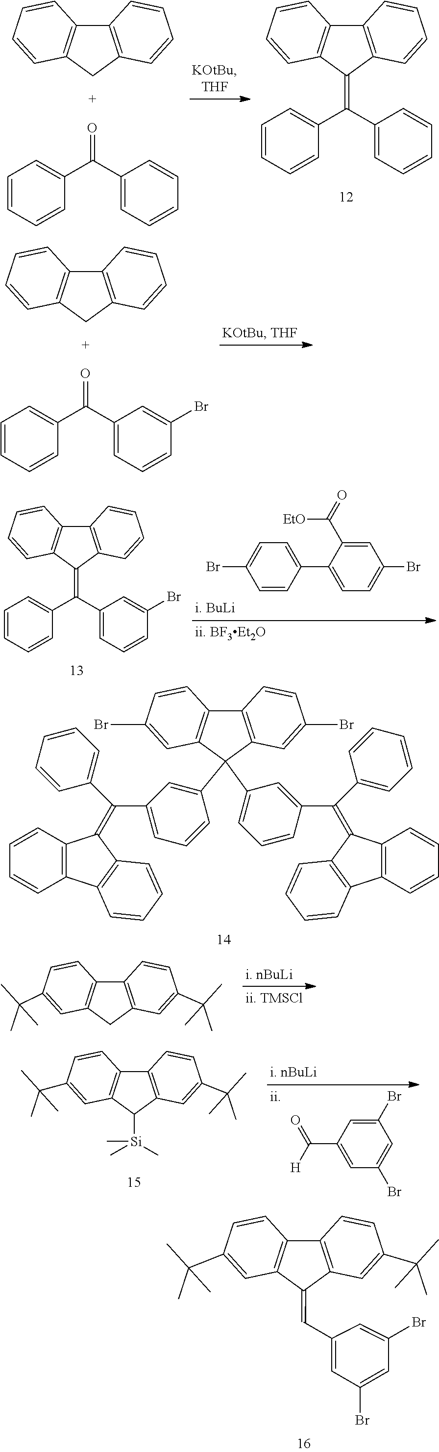
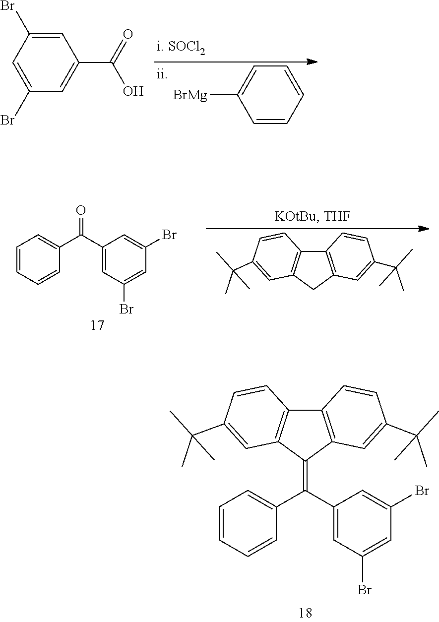


| Comparative | | Polymer | |
| Polymer | |||
| 1 | Example 1 | Example 2 | |
| Monomer | mol % | mol % | mol % |
 |
36 | 36 | 36 |
 |
14 | 14 | 14 |
 |
44 | 43.65 | 43.65 |
 |
5 | 5 | 5 |
 |
1 | 1 | 1 |
 |
0 | 0.35 | 0. |
 |
0 | 0 | 0.35 |


Claims (18)


Applications Claiming Priority (11)
| Application Number | Priority Date | Filing Date | Title |
|---|---|---|---|
| GBGB1010741.5A GB201010741D0 (en) | 2010-06-25 | 2010-06-25 | Organic light-emitting device and method |
| GB1010745.6A GB2483629A (en) | 2010-06-25 | 2010-06-25 | Light-emitting polymer and triplet-accepting unit |
| GB1010741.5 | 2010-06-25 | ||
| GB1010742.3 | 2010-06-25 | ||
| GB1010743.1 | 2010-06-25 | ||
| GB1010742.3A GB2483628A (en) | 2010-06-25 | 2010-06-25 | Organic Light-Emitting Composition |
| GB1010745.6 | 2010-06-25 | ||
| GBGB1010743.1A GB201010743D0 (en) | 2010-06-25 | 2010-06-25 | Organic light-emitting device and method |
| GB1101642.5A GB2499969A (en) | 2010-06-25 | 2011-01-31 | Composition comprising an organic semiconducting material and a triplet-accepting material |
| GB1101642.5 | 2011-01-31 | ||
| PCT/GB2011/000950 WO2011161417A1 (en) | 2010-06-25 | 2011-06-24 | Organic light-emitting material device and method |
Publications (2)
| Publication Number | Publication Date |
|---|---|
| US20130200348A1 US20130200348A1 (en) | 2013-08-08 |
| US9142782B2 true US9142782B2 (en) | 2015-09-22 |
Family
ID=44511799
Family Applications (4)
| Application Number | Title | Priority Date | Filing Date |
|---|---|---|---|
| US13/805,297 Active 2034-12-21 US9812647B2 (en) | 2010-06-25 | 2011-06-24 | Organic light-emitting device and method |
| US13/805,764 Active 2034-12-17 US9773981B2 (en) | 2010-06-25 | 2011-06-24 | Organic light-emitting device and method |
| US13/805,268 Active 2031-07-13 US9142782B2 (en) | 2010-06-25 | 2011-06-24 | Organic light-emitting material, device and method |
| US13/805,285 Abandoned US20130187145A1 (en) | 2010-06-25 | 2011-06-24 | Organic light-emitting composition comprising anthranthene derivates and device and method using the same |
Family Applications Before (2)
| Application Number | Title | Priority Date | Filing Date |
|---|---|---|---|
| US13/805,297 Active 2034-12-21 US9812647B2 (en) | 2010-06-25 | 2011-06-24 | Organic light-emitting device and method |
| US13/805,764 Active 2034-12-17 US9773981B2 (en) | 2010-06-25 | 2011-06-24 | Organic light-emitting device and method |
Family Applications After (1)
| Application Number | Title | Priority Date | Filing Date |
|---|---|---|---|
| US13/805,285 Abandoned US20130187145A1 (en) | 2010-06-25 | 2011-06-24 | Organic light-emitting composition comprising anthranthene derivates and device and method using the same |
Country Status (7)
| Country | Link |
|---|---|
| US (4) | US9812647B2 (en) |
| EP (1) | EP2586076B2 (en) |
| KR (2) | KR101916479B1 (en) |
| CN (4) | CN102959757B (en) |
| DE (2) | DE112011102127B4 (en) |
| GB (3) | GB2495250A (en) |
| WO (4) | WO2011161416A2 (en) |
Cited By (4)
| Publication number | Priority date | Publication date | Assignee | Title |
|---|---|---|---|---|
| US10032987B2 (en) | 2013-06-11 | 2018-07-24 | Canon Kabushiki Kaisha | Organic light emitting element |
| US10128455B2 (en) | 2013-05-16 | 2018-11-13 | Semiconductor Energy Laboratory Co., Ltd. | Light-emitting element, light-emitting device, electronic device, and lighting device |
| US10862041B2 (en) | 2014-10-31 | 2020-12-08 | Semiconductor Energy Laboratory Co., Ltd. | Benzo[a]anthracene compound, light-emitting element, display device, electronic device, and lighting device |
| US11937498B2 (en) | 2018-05-31 | 2024-03-19 | Semiconductor Energy Laboratory Co., Ltd. | Organic compound, light-emitting device, light-emitting apparatus, electronic apparatus, and lighting apparatus |
Families Citing this family (19)
| Publication number | Priority date | Publication date | Assignee | Title |
|---|---|---|---|---|
| WO2011161416A2 (en) | 2010-06-25 | 2011-12-29 | Cambridge Display Technology Limited | Organic light-emitting composition, device and method |
| GB2484680B (en) * | 2010-10-19 | 2013-06-05 | Cambridge Display Tech Ltd | Polymer and organic light-emitting device |
| GB2494096B (en) * | 2011-01-31 | 2013-12-18 | Cambridge Display Tech Ltd | Polymer |
| JP5487174B2 (en) * | 2011-09-16 | 2014-05-07 | 株式会社東芝 | Organic electroluminescent element, display device and lighting device |
| GB2501032A (en) * | 2012-01-26 | 2013-10-09 | Cambridge Display Tech Ltd | Polymer |
| GB2508409B (en) * | 2012-11-30 | 2015-11-25 | Cambridge Display Tech Ltd | Organic light-emitting composition, device and method |
| GB201207866D0 (en) * | 2012-05-04 | 2012-06-20 | Cambridge Display Tech Ltd | Organic light emitting device and method |
| KR20150122754A (en) | 2013-03-29 | 2015-11-02 | 코니카 미놀타 가부시키가이샤 | Organic electroluminescent element, lighting device, display device, light-emitting thin film and composition for organic electroluminescent element, and light-emitting method |
| WO2014163083A1 (en) | 2013-04-05 | 2014-10-09 | コニカミノルタ株式会社 | Coating liquid for forming light emitting layer, organic electroluminescent element, method for manufacturing organic electroluminescent element, and lighting/display device |
| US10193094B2 (en) | 2013-04-08 | 2019-01-29 | Merck Patent Gmbh | Organic light-emitting device having delayed fluorescence |
| CN103500803B (en) * | 2013-10-21 | 2016-06-08 | 京东方科技集团股份有限公司 | A kind of recombination luminescence layer and making method, white light organic electroluminescent device |
| CN103525406B (en) | 2013-10-21 | 2015-08-26 | 京东方科技集团股份有限公司 | A kind of laminated film and preparation method thereof, sealed cell and optoelectronic device |
| CN106232769B (en) * | 2014-04-23 | 2019-05-03 | 住友化学株式会社 | Composition and the light-emitting component for using the composition |
| GB2529668A (en) * | 2014-08-28 | 2016-03-02 | Cambridge Display Tech Ltd | Organic light-emitting composition, device and method |
| KR102460646B1 (en) | 2014-09-16 | 2022-10-31 | 삼성디스플레이 주식회사 | Light―emitting layer suitable for bright luminescence |
| GB2530748A (en) * | 2014-09-30 | 2016-04-06 | Cambridge Display Tech Ltd | Organic Light Emitting Device |
| CN113937228A (en) * | 2015-12-01 | 2022-01-14 | 株式会社半导体能源研究所 | Light-emitting element, light-emitting device, electronic device, and lighting device |
| KR20200100879A (en) | 2019-02-15 | 2020-08-27 | 삼성디스플레이 주식회사 | Organic light emitting device and electronic apparatus comprising the same |
| KR20200133138A (en) | 2019-05-17 | 2020-11-26 | 삼성디스플레이 주식회사 | Arylamine compound and organic light emitting device including the same |
Citations (53)
| Publication number | Priority date | Publication date | Assignee | Title |
|---|---|---|---|---|
| FR2151005A1 (en) | 1971-09-01 | 1973-04-13 | Ciba Geigy Ag | |
| US4769304A (en) | 1981-04-27 | 1988-09-06 | Fuji Photo Film Co., Ltd. | Photoconductive composition and electro-photographic light-sensitive material using said composition |
| US5998045A (en) | 1997-07-03 | 1999-12-07 | International Business Machines Corporation | Polymeric light-emitting device |
| JP2000164359A (en) | 1998-11-25 | 2000-06-16 | Idemitsu Kosan Co Ltd | Organic electroluminescent element |
| WO2000055927A1 (en) | 1999-03-12 | 2000-09-21 | Cambridge Display Technology Limited | Polymers, their preparation and uses |
| WO2001083410A1 (en) | 2000-05-03 | 2001-11-08 | The Regents Of The University Of California | Soluble tetrahedral compounds for use in electroluminescent devices |
| US20010053842A1 (en) * | 1995-07-28 | 2001-12-20 | Woo Edmund P. | 2,7-aryl-9-substituted fluorenes and 9-substituted fluorene oligomers and polymers |
| US6353083B1 (en) | 1999-02-04 | 2002-03-05 | The Dow Chemical Company | Fluorene copolymers and devices made therefrom |
| US20020048688A1 (en) | 2000-03-30 | 2002-04-25 | Idemitsu Kosan Co., Ltd. | Organic electroluminescence device and organic light emitting medium |
| US20020185635A1 (en) * | 2001-04-27 | 2002-12-12 | Sumitomo Chemical Company, Limited | Polymeric fluorescent substance and polymer light-emitting device using the same |
| US20030068527A1 (en) * | 2001-07-19 | 2003-04-10 | Sumitomo Chemical Company, Limited | Polymeric fluorescent substrate and polymer light-emitting device using the same |
| US20030082404A1 (en) | 2001-08-29 | 2003-05-01 | Fujitsu Limited | Condensed eight-ring aromatic compound, and organic EL element and organic EL display using the same |
| US20030088043A1 (en) * | 2001-06-21 | 2003-05-08 | Wei Huang | Light-emitting polymers and polymer light-emitting diodes |
| US20030143429A1 (en) * | 2001-12-19 | 2003-07-31 | Sumitomo Chemical Company, Limited | Copolymer, polymer composition and polymer light-emitting device |
| US20030165716A1 (en) * | 1997-10-23 | 2003-09-04 | Samuel Ifor David | Light-emitting dendrimers |
| EP1359790A2 (en) | 2002-04-24 | 2003-11-05 | Eastman Kodak Company | Organic light-emitting diode devices with improved operational stability |
| US20040137263A1 (en) * | 2001-02-20 | 2004-07-15 | Burn Paul Leslie | Metal-containing dendrimers |
| EP1440959A1 (en) | 2001-10-31 | 2004-07-28 | Idemitsu Kosan Co., Ltd. | Novel soluble compound and organic electroluminescent devices |
| EP1487027A2 (en) | 2003-06-10 | 2004-12-15 | Samsung SDI Co., Ltd. | OLED device and OLED-based display with improved efficiency |
| US20050048313A1 (en) | 2003-08-29 | 2005-03-03 | Fujitsu Limited | Fluorescent material, organic electroluminescent element and organic electroluminescent display |
| US20050089714A1 (en) | 2003-10-22 | 2005-04-28 | Eastman Kodak Company | Stabilized white-light-emitting OLED device |
| US20050095456A1 (en) | 2003-10-01 | 2005-05-05 | International Business Machines Corporation | Organic electroluminescence device and method of manufacture |
| US20050096491A1 (en) | 2002-02-06 | 2005-05-05 | Matsushita Electric Industrial Co., Ltd. | Aromatic methylidene compound, methylstyryl compound for producing the same, production method therefor, and organic electroluminescent element |
| US20050153167A1 (en) * | 2002-07-22 | 2005-07-14 | Sumitomo Chemical Company, Limited | Copolymer and polymer light emitting device using the same |
| US20050164029A1 (en) * | 2002-08-29 | 2005-07-28 | Burn Paul L. | Reactive dendrimers |
| US20050212409A1 (en) | 2004-03-23 | 2005-09-29 | Jianmmin Shi | Organic luminescent materials |
| US20050214566A1 (en) | 2004-03-23 | 2005-09-29 | Jianmin Shi | Organic electroluminescent devices |
| US20060040131A1 (en) | 2004-08-19 | 2006-02-23 | Eastman Kodak Company | OLEDs with improved operational lifetime |
| JP2006243626A (en) | 2005-03-07 | 2006-09-14 | Ricoh Co Ltd | Light wavelength converting element |
| JP2006253221A (en) | 2005-03-08 | 2006-09-21 | Ricoh Co Ltd | Organic semiconductor laser |
| US20060229427A1 (en) * | 2003-08-12 | 2006-10-12 | Heinrick Becker | Conjugated copolymers, representation and use thereof |
| US20060240565A1 (en) | 2005-04-22 | 2006-10-26 | Tang Ben Z | Environment sensor and conjugated polyene for manufacturing environment sensors |
| US7205366B2 (en) | 2002-04-02 | 2007-04-17 | E. I. Du Pont De Nemours And Company | Hole transport polymers and devices made with such polymers |
| US20070145886A1 (en) | 2005-12-27 | 2007-06-28 | Lg. Philips Lcd Co., Ltd. | Organic light emitting devices |
| CN101016248A (en) | 2006-12-29 | 2007-08-15 | 清华大学 | Organic electroluminescent material and application thereof |
| US20070244295A1 (en) | 2006-04-13 | 2007-10-18 | Seiko Epson Corporation | Compound for Organic Electroluminescence and Organic Electroluminescent Device |
| CN101279888A (en) | 2008-05-20 | 2008-10-08 | 吉林大学 | 9,10-divinyl anthracene derivate and application thereof to organic electroluminescent devices |
| US20090066238A1 (en) * | 2007-09-06 | 2009-03-12 | National Tsing Hua University | Electroluminescent materials grafted with charge transport moieties having graded ionization potential or electrophilic property and their application in light-emitting diodes |
| GB2456788A (en) | 2008-01-23 | 2009-07-29 | Cambridge Display Tech Ltd | White light emitting material |
| US20090191428A1 (en) | 2008-01-30 | 2009-07-30 | Hatwar Tukaram K | Tandem oled device with intermediate connector |
| US20090308456A1 (en) | 2008-06-13 | 2009-12-17 | Interuniversitair Microelektronica Centrum (Imec) | Photovoltaic Structures and Method to Produce the Same |
| CN101624441A (en) | 2009-07-24 | 2010-01-13 | 南京邮电大学 | Preparation method and application method of 4-9, 9-diaryl fluorene polymer material containing substituted radical |
| WO2010013006A2 (en) | 2008-08-01 | 2010-02-04 | Cambridge Display Technology Limited | Blue-light emitting material |
| GB2463040A (en) | 2008-08-28 | 2010-03-03 | Cambridge Display Tech Ltd | Light emitting polymer |
| US20110042658A1 (en) | 2009-07-01 | 2011-02-24 | Sony Corporation | Anthanthrene based compound and semiconductor device |
| US20120008068A1 (en) * | 2002-10-30 | 2012-01-12 | Sumitomo Chemical Company, Limited | Polymer compound and polymer light-emitting device using the same |
| US20120091449A1 (en) * | 2009-06-23 | 2012-04-19 | Sumitomo Chemical Company, Limited | Organic electroluminescent element |
| US20120112170A1 (en) * | 2009-01-28 | 2012-05-10 | University Of Washington | Cross-conjugated polymers for organic electronic devices and related methods |
| US20120116050A1 (en) | 2009-06-15 | 2012-05-10 | Technische Universitaet Graz | Pyrene-based polymers for organic light emitting diodes (oleds) |
| US20130146813A1 (en) | 2005-02-04 | 2013-06-13 | Konica Minolta Holdings, Inc. | Material for organic electroluminescence element, organic electroluminescence element, display device and lighting device |
| US20130187147A1 (en) | 2010-06-25 | 2013-07-25 | Sumitomo Chemical Company Limited | Organic light-emitting device and method |
| US20130270535A1 (en) | 2010-10-19 | 2013-10-17 | Sumitomo Chemical Company Limited | Polymer and organic light-emitting device |
| US20140103303A1 (en) * | 2010-07-12 | 2014-04-17 | David L. Carroll | Conjugated Polymeric Systems And Applications Thereof |
Family Cites Families (38)
| Publication number | Priority date | Publication date | Assignee | Title |
|---|---|---|---|---|
| GB252010A (en) | 1925-05-09 | 1927-01-13 | British Thomson Houston Co Ltd | Improvements in and relating to regulating systems for dynamo-electric-machines |
| GB1010741A (en) | 1960-11-02 | 1965-11-24 | Monsanto Co | Esters of thiocarbamic acid |
| NL272286A (en) | 1960-12-27 | |||
| GB1010745A (en) | 1963-04-10 | 1965-11-24 | Ici Ltd | New water-insoluble anthraquinone dyestuffs |
| FR1392566A (en) | 1964-01-23 | 1965-03-19 | Csf | VHF isolator on coaxial line |
| US4539507A (en) | 1983-03-25 | 1985-09-03 | Eastman Kodak Company | Organic electroluminescent devices having improved power conversion efficiencies |
| US4806444A (en) | 1987-06-10 | 1989-02-21 | Xerox Corporation | Arylamine polymers and systems utilizing arylamine polymers |
| US5121029A (en) | 1987-12-11 | 1992-06-09 | Idemitsu Kosan Co., Ltd. | Electroluminescence device having an organic electroluminescent element |
| GB8909011D0 (en) | 1989-04-20 | 1989-06-07 | Friend Richard H | Electroluminescent devices |
| US5723873A (en) | 1994-03-03 | 1998-03-03 | Yang; Yang | Bilayer composite electrodes for diodes |
| DE4436773A1 (en) | 1994-10-14 | 1996-04-18 | Hoechst Ag | Conjugated polymers with spirocenters and their use as electroluminescent materials |
| WO1997005184A1 (en) | 1995-07-28 | 1997-02-13 | The Dow Chemical Company | 2,7-aryl-9-substituted fluorenes and 9-substituted fluorene oligomers and polymers |
| US5798170A (en) | 1996-02-29 | 1998-08-25 | Uniax Corporation | Long operating life for polymer light-emitting diodes |
| DE69710781T2 (en) | 1996-07-29 | 2002-10-31 | Cambridge Display Tech Ltd | ELECTROLUMINESCENT ARRANGEMENTS WITH ELECTRODE PROTECTION |
| DE69724129T2 (en) | 1996-09-04 | 2004-02-26 | Cambridge Display Technology Ltd. | LIGHT-EMITTING ORGANIC DEVICES WITH IMPROVED CATHODE |
| JP3899566B2 (en) | 1996-11-25 | 2007-03-28 | セイコーエプソン株式会社 | Manufacturing method of organic EL display device |
| US6452218B1 (en) | 1997-06-10 | 2002-09-17 | Uniax Corporation | Ultra-thin alkaline earth metals as stable electron-injecting electrodes for polymer light emitting diodes |
| GB9718393D0 (en) | 1997-08-29 | 1997-11-05 | Cambridge Display Tech Ltd | Electroluminescent Device |
| GB9805476D0 (en) | 1998-03-13 | 1998-05-13 | Cambridge Display Tech Ltd | Electroluminescent devices |
| GB2335884A (en) | 1998-04-02 | 1999-10-06 | Cambridge Display Tech Ltd | Flexible substrates for electronic or optoelectronic devices |
| US6268695B1 (en) | 1998-12-16 | 2001-07-31 | Battelle Memorial Institute | Environmental barrier material for organic light emitting device and method of making |
| GB9903251D0 (en) | 1999-02-12 | 1999-04-07 | Cambridge Display Tech Ltd | Opto-electric devices |
| DE60035970T2 (en) | 1999-03-05 | 2008-05-15 | Cambridge Display Technology Ltd. | Polymer Preparation |
| GB2348316A (en) | 1999-03-26 | 2000-09-27 | Cambridge Display Tech Ltd | Organic opto-electronic device |
| FR2797714B1 (en) | 1999-08-20 | 2001-10-26 | Soitec Silicon On Insulator | PROCESS FOR PROCESSING SUBSTRATES FOR MICROELECTRONICS AND SUBSTRATES OBTAINED BY THIS PROCESS |
| CN1385053A (en) | 1999-09-03 | 2002-12-11 | 优尼爱克斯公司 | Encapsulation of organic electronic devices |
| US6413645B1 (en) | 2000-04-20 | 2002-07-02 | Battelle Memorial Institute | Ultrabarrier substrates |
| KR20030024690A (en) | 2001-04-17 | 2003-03-26 | 코닌클리케 필립스 일렉트로닉스 엔.브이. | Led comprising a conductive transparent polymer layer with low sulfate and high metal ion content |
| EP1426399A4 (en) * | 2001-09-04 | 2005-07-13 | Canon Kk | High-molecular compounds and organic luminescent devices |
| WO2003079408A2 (en) | 2002-03-12 | 2003-09-25 | I & K Trading | Portable light-emitting display device |
| AU2003303067A1 (en) * | 2002-12-13 | 2004-07-09 | Koninklijke Philips Electronics N.V. | Electroluminescent device |
| JP2006520409A (en) * | 2003-02-12 | 2006-09-07 | コーニンクレッカ フィリップス エレクトロニクス エヌ ヴィ | Carbazole compounds and the use of such compounds in organic electroluminescent devices |
| US20060141287A1 (en) | 2004-08-19 | 2006-06-29 | Eastman Kodak Company | OLEDs with improved operational lifetime |
| GB0507684D0 (en) | 2005-04-15 | 2005-05-25 | Cambridge Display Tech Ltd | Pulsed driven displays |
| JPWO2007116828A1 (en) | 2006-04-03 | 2009-08-20 | 出光興産株式会社 | Bisanthracene derivative and organic electroluminescence device using the same |
| GB0803950D0 (en) * | 2008-03-03 | 2008-04-09 | Cambridge Display Technology O | Solvent for printing composition |
| JP5609024B2 (en) | 2008-06-30 | 2014-10-22 | 住友化学株式会社 | Phenoxazine-based polymer compound and light emitting device using the same |
| US9196853B2 (en) * | 2009-01-08 | 2015-11-24 | Katholieke Universiteit Leuven, K.U. Leuven R&D | Triplet excitation scavenging in solid-state organic materials |
-
2011
- 2011-06-24 WO PCT/GB2011/000949 patent/WO2011161416A2/en active Application Filing
- 2011-06-24 US US13/805,297 patent/US9812647B2/en active Active
- 2011-06-24 GB GB1300532.7A patent/GB2495250A/en not_active Withdrawn
- 2011-06-24 US US13/805,764 patent/US9773981B2/en active Active
- 2011-06-24 WO PCT/GB2011/000950 patent/WO2011161417A1/en active Application Filing
- 2011-06-24 KR KR1020137001777A patent/KR101916479B1/en active IP Right Grant
- 2011-06-24 WO PCT/GB2011/000961 patent/WO2011161424A1/en active Application Filing
- 2011-06-24 GB GB1300531.9A patent/GB2496771B/en not_active Expired - Fee Related
- 2011-06-24 GB GB1300535.0A patent/GB2494367B/en not_active Expired - Fee Related
- 2011-06-24 WO PCT/GB2011/000962 patent/WO2011161425A1/en active Application Filing
- 2011-06-24 CN CN201180031403.7A patent/CN102959757B/en active Active
- 2011-06-24 CN CN2011800314107A patent/CN103069605A/en active Pending
- 2011-06-24 DE DE112011102127.5T patent/DE112011102127B4/en active Active
- 2011-06-24 KR KR1020137001924A patent/KR20130038905A/en not_active Application Discontinuation
- 2011-06-24 US US13/805,268 patent/US9142782B2/en active Active
- 2011-06-24 DE DE112011102126T patent/DE112011102126T5/en not_active Withdrawn
- 2011-06-24 CN CN201180038121.XA patent/CN103038910B/en active Active
- 2011-06-24 US US13/805,285 patent/US20130187145A1/en not_active Abandoned
- 2011-06-24 EP EP11744049.5A patent/EP2586076B2/en active Active
- 2011-06-24 CN CN201180031602.8A patent/CN102959758B/en active Active
Patent Citations (60)
| Publication number | Priority date | Publication date | Assignee | Title |
|---|---|---|---|---|
| US3907904A (en) | 1971-09-01 | 1975-09-23 | Ciba Geigy Ag | Optical brighteners comprising alkoxy derivatives of distyryldiphenyl |
| FR2151005A1 (en) | 1971-09-01 | 1973-04-13 | Ciba Geigy Ag | |
| US4769304A (en) | 1981-04-27 | 1988-09-06 | Fuji Photo Film Co., Ltd. | Photoconductive composition and electro-photographic light-sensitive material using said composition |
| US20010053842A1 (en) * | 1995-07-28 | 2001-12-20 | Woo Edmund P. | 2,7-aryl-9-substituted fluorenes and 9-substituted fluorene oligomers and polymers |
| US5998045A (en) | 1997-07-03 | 1999-12-07 | International Business Machines Corporation | Polymeric light-emitting device |
| US20030165716A1 (en) * | 1997-10-23 | 2003-09-04 | Samuel Ifor David | Light-emitting dendrimers |
| JP2000164359A (en) | 1998-11-25 | 2000-06-16 | Idemitsu Kosan Co Ltd | Organic electroluminescent element |
| US6353083B1 (en) | 1999-02-04 | 2002-03-05 | The Dow Chemical Company | Fluorene copolymers and devices made therefrom |
| US6861502B1 (en) | 1999-03-12 | 2005-03-01 | Dow Global Technologies Inc. | Polymers, their preparation and uses |
| WO2000055927A1 (en) | 1999-03-12 | 2000-09-21 | Cambridge Display Technology Limited | Polymers, their preparation and uses |
| US20020048688A1 (en) | 2000-03-30 | 2002-04-25 | Idemitsu Kosan Co., Ltd. | Organic electroluminescence device and organic light emitting medium |
| WO2001083410A1 (en) | 2000-05-03 | 2001-11-08 | The Regents Of The University Of California | Soluble tetrahedral compounds for use in electroluminescent devices |
| US20040137263A1 (en) * | 2001-02-20 | 2004-07-15 | Burn Paul Leslie | Metal-containing dendrimers |
| US20020185635A1 (en) * | 2001-04-27 | 2002-12-12 | Sumitomo Chemical Company, Limited | Polymeric fluorescent substance and polymer light-emitting device using the same |
| US20030088043A1 (en) * | 2001-06-21 | 2003-05-08 | Wei Huang | Light-emitting polymers and polymer light-emitting diodes |
| US20030068527A1 (en) * | 2001-07-19 | 2003-04-10 | Sumitomo Chemical Company, Limited | Polymeric fluorescent substrate and polymer light-emitting device using the same |
| US20030082404A1 (en) | 2001-08-29 | 2003-05-01 | Fujitsu Limited | Condensed eight-ring aromatic compound, and organic EL element and organic EL display using the same |
| EP1440959A1 (en) | 2001-10-31 | 2004-07-28 | Idemitsu Kosan Co., Ltd. | Novel soluble compound and organic electroluminescent devices |
| US20030143429A1 (en) * | 2001-12-19 | 2003-07-31 | Sumitomo Chemical Company, Limited | Copolymer, polymer composition and polymer light-emitting device |
| US20050096491A1 (en) | 2002-02-06 | 2005-05-05 | Matsushita Electric Industrial Co., Ltd. | Aromatic methylidene compound, methylstyryl compound for producing the same, production method therefor, and organic electroluminescent element |
| US7205366B2 (en) | 2002-04-02 | 2007-04-17 | E. I. Du Pont De Nemours And Company | Hole transport polymers and devices made with such polymers |
| EP1359790A2 (en) | 2002-04-24 | 2003-11-05 | Eastman Kodak Company | Organic light-emitting diode devices with improved operational stability |
| US20050153167A1 (en) * | 2002-07-22 | 2005-07-14 | Sumitomo Chemical Company, Limited | Copolymer and polymer light emitting device using the same |
| US20050164029A1 (en) * | 2002-08-29 | 2005-07-28 | Burn Paul L. | Reactive dendrimers |
| US20120008068A1 (en) * | 2002-10-30 | 2012-01-12 | Sumitomo Chemical Company, Limited | Polymer compound and polymer light-emitting device using the same |
| EP1487027A2 (en) | 2003-06-10 | 2004-12-15 | Samsung SDI Co., Ltd. | OLED device and OLED-based display with improved efficiency |
| US20060229427A1 (en) * | 2003-08-12 | 2006-10-12 | Heinrick Becker | Conjugated copolymers, representation and use thereof |
| US20050048313A1 (en) | 2003-08-29 | 2005-03-03 | Fujitsu Limited | Fluorescent material, organic electroluminescent element and organic electroluminescent display |
| US20050095456A1 (en) | 2003-10-01 | 2005-05-05 | International Business Machines Corporation | Organic electroluminescence device and method of manufacture |
| WO2005043640A2 (en) | 2003-10-22 | 2005-05-12 | Eastman Kodak Company | A stabilized white-light emitting oled |
| US20050089714A1 (en) | 2003-10-22 | 2005-04-28 | Eastman Kodak Company | Stabilized white-light-emitting OLED device |
| US20050214566A1 (en) | 2004-03-23 | 2005-09-29 | Jianmin Shi | Organic electroluminescent devices |
| US20050212409A1 (en) | 2004-03-23 | 2005-09-29 | Jianmmin Shi | Organic luminescent materials |
| US20060040131A1 (en) | 2004-08-19 | 2006-02-23 | Eastman Kodak Company | OLEDs with improved operational lifetime |
| US20130146813A1 (en) | 2005-02-04 | 2013-06-13 | Konica Minolta Holdings, Inc. | Material for organic electroluminescence element, organic electroluminescence element, display device and lighting device |
| JP2006243626A (en) | 2005-03-07 | 2006-09-14 | Ricoh Co Ltd | Light wavelength converting element |
| JP2006253221A (en) | 2005-03-08 | 2006-09-21 | Ricoh Co Ltd | Organic semiconductor laser |
| US20060240565A1 (en) | 2005-04-22 | 2006-10-26 | Tang Ben Z | Environment sensor and conjugated polyene for manufacturing environment sensors |
| US20070145886A1 (en) | 2005-12-27 | 2007-06-28 | Lg. Philips Lcd Co., Ltd. | Organic light emitting devices |
| US20070244295A1 (en) | 2006-04-13 | 2007-10-18 | Seiko Epson Corporation | Compound for Organic Electroluminescence and Organic Electroluminescent Device |
| CN101016248A (en) | 2006-12-29 | 2007-08-15 | 清华大学 | Organic electroluminescent material and application thereof |
| US20090066238A1 (en) * | 2007-09-06 | 2009-03-12 | National Tsing Hua University | Electroluminescent materials grafted with charge transport moieties having graded ionization potential or electrophilic property and their application in light-emitting diodes |
| GB2456788A (en) | 2008-01-23 | 2009-07-29 | Cambridge Display Tech Ltd | White light emitting material |
| US20090191428A1 (en) | 2008-01-30 | 2009-07-30 | Hatwar Tukaram K | Tandem oled device with intermediate connector |
| CN101279888A (en) | 2008-05-20 | 2008-10-08 | 吉林大学 | 9,10-divinyl anthracene derivate and application thereof to organic electroluminescent devices |
| US20090308456A1 (en) | 2008-06-13 | 2009-12-17 | Interuniversitair Microelektronica Centrum (Imec) | Photovoltaic Structures and Method to Produce the Same |
| WO2010013006A2 (en) | 2008-08-01 | 2010-02-04 | Cambridge Display Technology Limited | Blue-light emitting material |
| US20110186828A1 (en) | 2008-08-01 | 2011-08-04 | Cambridge Display Technology Limited | Blue light-Emitting Material |
| GB2463040A (en) | 2008-08-28 | 2010-03-03 | Cambridge Display Tech Ltd | Light emitting polymer |
| US20120112170A1 (en) * | 2009-01-28 | 2012-05-10 | University Of Washington | Cross-conjugated polymers for organic electronic devices and related methods |
| US20120116050A1 (en) | 2009-06-15 | 2012-05-10 | Technische Universitaet Graz | Pyrene-based polymers for organic light emitting diodes (oleds) |
| US20120091449A1 (en) * | 2009-06-23 | 2012-04-19 | Sumitomo Chemical Company, Limited | Organic electroluminescent element |
| US20110042658A1 (en) | 2009-07-01 | 2011-02-24 | Sony Corporation | Anthanthrene based compound and semiconductor device |
| US20130099223A1 (en) | 2009-07-01 | 2013-04-25 | Sony Corporation | Anthanthrene based compound and semiconductor device |
| CN101624441A (en) | 2009-07-24 | 2010-01-13 | 南京邮电大学 | Preparation method and application method of 4-9, 9-diaryl fluorene polymer material containing substituted radical |
| US20130187147A1 (en) | 2010-06-25 | 2013-07-25 | Sumitomo Chemical Company Limited | Organic light-emitting device and method |
| US20130187146A1 (en) * | 2010-06-25 | 2013-07-25 | Sumitomo Chemical Company Limited | Organic light-emitting device and method |
| US20130187145A1 (en) | 2010-06-25 | 2013-07-25 | Sumitomo Chemical Company Limited | Organic light-emitting composition comprising anthranthene derivates and device and method using the same |
| US20140103303A1 (en) * | 2010-07-12 | 2014-04-17 | David L. Carroll | Conjugated Polymeric Systems And Applications Thereof |
| US20130270535A1 (en) | 2010-10-19 | 2013-10-17 | Sumitomo Chemical Company Limited | Polymer and organic light-emitting device |
Non-Patent Citations (28)
| Title |
|---|
| Becker et al., Optimisation of polyfluorenes for light emitting applications. Synthetic Metals. 2001;125(1):73-8. |
| Bernius et al., Progress with Light-Emitting Polymers. Advanced Materials. 2000;12(23):1737-50. |
| CAS Registry No. 31927-64-7. |
| Chen et al., Connector Effect in Electroluminescent Properties of Poly(p-phenylene vinylene) Derivatives Containing Triazole Chromophores. Macromolecular Chemistry and Physics. 2006;207(12):1070-9. |
| Chen et al., White organic light-emitting devices with a bipolar transport layer between blue fluorescent and orange phosphorescent emitting layers. Applied Physics Letters. 2007; 91:023505. 3 pages. |
| Ego et al., Attaching perylene dyes to polyfluorene: three simple, efficient methods for facile color tuning of light-emitting polymers. J Am Chem Soc. Jan. 15, 2003;125(2):437-43. |
| Exam Report for corresponding European application No. 11744049.5, dated Apr. 2, 2014, pp. 1-11. |
| International Preliminary Report on Patentability mailed Jan. 10, 2013 for International Application No. PCT/GB2011/000949. |
| International Preliminary Report on Patentability mailed Jan. 10, 2013 for International Application No. PCT/GB2011/000950. |
| International Preliminary Report on Patentability mailed Jan. 10, 2013 for International Application No. PCT/GB2011/000961. |
| International Preliminary Report on Patentability mailed Jan. 10, 2013 for International Application No. PCT/GB2011/000962. |
| International Search Report and Written Opinion mailed Jan. 20, 2012 for International Application No. PCT/GB2011/000949. |
| International Search Report and Written Opinion mailed Sep. 27, 2011 for International Application No. PCT/GB2011/000950. |
| International Search Report and Written Opinion mailed Sep. 27, 2011 for International Application No. PCT/GB2011/000962. |
| International Search Report and Written Opinion mailed Sep. 29, 2011 for International Application No. PCT/GB2011/000961. |
| Kang et al., Very large electro-optic coefficients from in situ generated side-chain nonlinear optical polymers. Appl Phys Lett. 2005;87:71109. |
| Klärner et al., Exciton Migration and Trapping in Copolymers Based on Dialkylfluorenes Advanced Materials. 1999;11(2):115-9. |
| Kuo et al., Journal of Polymer Science: Part A: Polymer Chemistry, vol. 45, 4504-4513, 2007). * |
| Lee et al., Color tuning in polyfluorenes by copolymerization with low band gap comonomers. Synthetic Metals. 1999;102(1-3):1087-8. |
| Lee et al., Investigation of Blue Organic Light-Emitting Diodes (OLEDs) with Various Hosts. J Korean Phys Soc. 2006;49(3):1052-6. |
| Liu et al., Molecular Design on Highly Efficient White Electroluminescence from a Single-Polymer System with Simultaneous Blue, Green, and Red Emission. Advanced Materials. 2007;19(4):531-5. |
| Mills et al., Dications of fluorenylidenes. Relationship between electrochemical oxidation potentials and antiaromaticity in diphenyl-substituted fluorenyl cations. J Org Chem. Apr. 5, 2002;67(7):2003-12. |
| Office Communication for EP 11744049.5 mailed Nov. 20, 2014. |
| Peng et al., Study on the energy transfer and luminescent properties in PVK: DBVP blend system. Acta Phys Sin. 2006;55(10):5495-8. |
| Popovic et al., Delayed Electroluminescence in Small Molecule Based Organic Light Emitting Diodes-Evidence for Triplet-Triplet Annihilation and Recombination Center Mediated Light Generation Mechanism. J App Phys. 2005;98:013510-5. |
| Shi et al., Anthanthrene Derivatives for Stable Blue-Emitting Organic Electroluminescent Devices. SID 05 Digest. 2005;36:1760-3. |
| Staroske et al., Single-step triplet-triplet annihilation: an intrinsic limit for the high brightness efficiency of phosphorescent organic light emitting diodes. Phys Rev Lett. May 11, 2007;98(19):197402. Epub May 10, 2007. |
| Thirunavukkarasu et al., One-Pot Synthesis of Diarylmethylidenefluorenes and Phenanthrenes by Palladium-Catalyzed Multiple C-H Bond Functionalization. Chemistry-A European Journal. 2010;16(5):1436-40. |
Cited By (8)
| Publication number | Priority date | Publication date | Assignee | Title |
|---|---|---|---|---|
| US10128455B2 (en) | 2013-05-16 | 2018-11-13 | Semiconductor Energy Laboratory Co., Ltd. | Light-emitting element, light-emitting device, electronic device, and lighting device |
| US11462701B2 (en) | 2013-05-16 | 2022-10-04 | Semiconductor Energy Laboratory Co., Ltd. | Light-emitting element, light-emitting device, electronic device, and lighting device |
| US10032987B2 (en) | 2013-06-11 | 2018-07-24 | Canon Kabushiki Kaisha | Organic light emitting element |
| US11139435B2 (en) | 2013-06-11 | 2021-10-05 | Canon Kabushiki Kaisha | Organic light emitting element |
| US10862041B2 (en) | 2014-10-31 | 2020-12-08 | Semiconductor Energy Laboratory Co., Ltd. | Benzo[a]anthracene compound, light-emitting element, display device, electronic device, and lighting device |
| US11563177B2 (en) | 2014-10-31 | 2023-01-24 | Semiconductor Energy Laboratory Co., Ltd. | Benzo[a]anthracene compound, light-emitting element, display device, electronic device, and lighting device |
| US11851594B2 (en) | 2014-10-31 | 2023-12-26 | Semiconductor Energy Laboratory Co., Ltd. | Benzo[a]anthracene compound, light-emitting element, display device, electronic device, and lighting device |
| US11937498B2 (en) | 2018-05-31 | 2024-03-19 | Semiconductor Energy Laboratory Co., Ltd. | Organic compound, light-emitting device, light-emitting apparatus, electronic apparatus, and lighting apparatus |
Also Published As
Similar Documents
| Publication | Publication Date | Title |
|---|---|---|
| US9142782B2 (en) | Organic light-emitting material, device and method | |
| US9562136B2 (en) | Polymers, monomers and methods of forming polymers | |
| EP2630675B1 (en) | Organic light-emitting device and method | |
| US9548467B2 (en) | Organic light-emitting device incorporating a triplet-triplet annihilation promoter and method of forming the same | |
| US9761820B2 (en) | Polymer | |
| US10985322B2 (en) | Polymer and organic light-emitting device | |
| JP6018052B2 (en) | Organic light emitting materials, devices and methods | |
| JP6713455B2 (en) | Organic light emitting compositions, devices and methods | |
| GB2483629A (en) | Light-emitting polymer and triplet-accepting unit | |
| GB2483628A (en) | Organic Light-Emitting Composition | |
| US10870726B2 (en) | Polymer | |
| WO2015079261A1 (en) | Polymer and organic light-emitting device | |
| US20170309837A1 (en) | Polymer and organic light-emitting device |
Legal Events
| Date | Code | Title | Description |
|---|---|---|---|
| AS | Assignment |
Owner name: CAMBRIDGE DISPLAY TECHNOLOGY, LTD., UNITED KINGDOM Free format text: ASSIGNMENT OF ASSIGNORS INTEREST;ASSIGNORS:PILLOW, JONATHAN;B?NNAGEL, TORSTEN;PINTANI, MARTINA;AND OTHERS;SIGNING DATES FROM 20130930 TO 20131002;REEL/FRAME:031327/0050 Owner name: SUMITOMO CHEMICAL COMPANY LIMITED, JAPAN Free format text: ASSIGNMENT OF ASSIGNORS INTEREST;ASSIGNORS:PILLOW, JONATHAN;B?NNAGEL, TORSTEN;PINTANI, MARTINA;AND OTHERS;SIGNING DATES FROM 20130930 TO 20131002;REEL/FRAME:031327/0050 |
|
| STCF | Information on status: patent grant |
Free format text: PATENTED CASE |
|
| MAFP | Maintenance fee payment |
Free format text: PAYMENT OF MAINTENANCE FEE, 4TH YEAR, LARGE ENTITY (ORIGINAL EVENT CODE: M1551); ENTITY STATUS OF PATENT OWNER: LARGE ENTITY Year of fee payment: 4 |
|
| MAFP | Maintenance fee payment |
Free format text: PAYMENT OF MAINTENANCE FEE, 8TH YEAR, LARGE ENTITY (ORIGINAL EVENT CODE: M1552); ENTITY STATUS OF PATENT OWNER: LARGE ENTITY Year of fee payment: 8 |