US9188740B1 - Unit cell based wavepath grid architecture applicable and to phased-array devices and enabling symmetrical output power distribution and single channel control - Google Patents

Unit cell based wavepath grid architecture applicable and to phased-array devices and enabling symmetrical output power distribution and single channel control Download PDF

Info

Publication number
US9188740B1
US9188740B1 US14/285,238 US201414285238A US9188740B1 US 9188740 B1 US9188740 B1 US 9188740B1 US 201414285238 A US201414285238 A US 201414285238A US 9188740 B1 US9188740 B1 US 9188740B1
Authority
US
United States
Prior art keywords
wavepath
waveguide
grid
recited
phase shift
Prior art date
Legal status (The legal status is an assumption and is not a legal conclusion. Google has not performed a legal analysis and makes no representation as to the accuracy of the status listed.)
Expired - Fee Related
Application number
US14/285,238
Other versions
US20150338576A1 (en
Inventor
Tsuyoshi Nomura
Current Assignee (The listed assignees may be inaccurate. Google has not performed a legal analysis and makes no representation or warranty as to the accuracy of the list.)
Toyota Central R&D Labs Inc
Original Assignee
Toyota Motor Engineering and Manufacturing North America Inc
Priority date (The priority date is an assumption and is not a legal conclusion. Google has not performed a legal analysis and makes no representation as to the accuracy of the date listed.)
Filing date
Publication date
Application filed by Toyota Motor Engineering and Manufacturing North America Inc filed Critical Toyota Motor Engineering and Manufacturing North America Inc
Priority to US14/285,238 priority Critical patent/US9188740B1/en
Assigned to TOYOTA MOTOR ENGINEERING & MANUFACTURING NORTH AMERICA, INC. reassignment TOYOTA MOTOR ENGINEERING & MANUFACTURING NORTH AMERICA, INC. ASSIGNMENT OF ASSIGNORS INTEREST (SEE DOCUMENT FOR DETAILS). Assignors: NOMURA, TSUYOSHI
Application granted granted Critical
Publication of US9188740B1 publication Critical patent/US9188740B1/en
Assigned to KABUSHIKI KAISHA TOYOTA CHUO KENKYUSHO reassignment KABUSHIKI KAISHA TOYOTA CHUO KENKYUSHO ASSIGNMENT OF ASSIGNORS INTEREST (SEE DOCUMENT FOR DETAILS). Assignors: TOYOTA MOTOR ENGINEERING & MANUFACTURING NORTH AMERICA, INC.
Publication of US20150338576A1 publication Critical patent/US20150338576A1/en
Expired - Fee Related legal-status Critical Current
Anticipated expiration legal-status Critical

Links

Images

Classifications

    • GPHYSICS
    • G02OPTICS
    • G02BOPTICAL ELEMENTS, SYSTEMS OR APPARATUS
    • G02B6/00Light guides; Structural details of arrangements comprising light guides and other optical elements, e.g. couplings
    • G02B6/10Light guides; Structural details of arrangements comprising light guides and other optical elements, e.g. couplings of the optical waveguide type
    • G02B6/12Light guides; Structural details of arrangements comprising light guides and other optical elements, e.g. couplings of the optical waveguide type of the integrated circuit kind
    • G02B6/122Basic optical elements, e.g. light-guiding paths
    • G02B6/125Bends, branchings or intersections
    • GPHYSICS
    • G02OPTICS
    • G02BOPTICAL ELEMENTS, SYSTEMS OR APPARATUS
    • G02B6/00Light guides; Structural details of arrangements comprising light guides and other optical elements, e.g. couplings
    • G02B6/10Light guides; Structural details of arrangements comprising light guides and other optical elements, e.g. couplings of the optical waveguide type
    • G02B6/12Light guides; Structural details of arrangements comprising light guides and other optical elements, e.g. couplings of the optical waveguide type of the integrated circuit kind
    • GPHYSICS
    • G02OPTICS
    • G02FOPTICAL DEVICES OR ARRANGEMENTS FOR THE CONTROL OF LIGHT BY MODIFICATION OF THE OPTICAL PROPERTIES OF THE MEDIA OF THE ELEMENTS INVOLVED THEREIN; NON-LINEAR OPTICS; FREQUENCY-CHANGING OF LIGHT; OPTICAL LOGIC ELEMENTS; OPTICAL ANALOGUE/DIGITAL CONVERTERS
    • G02F1/00Devices or arrangements for the control of the intensity, colour, phase, polarisation or direction of light arriving from an independent light source, e.g. switching, gating or modulating; Non-linear optics
    • G02F1/29Devices or arrangements for the control of the intensity, colour, phase, polarisation or direction of light arriving from an independent light source, e.g. switching, gating or modulating; Non-linear optics for the control of the position or the direction of light beams, i.e. deflection
    • G02F1/295Analog deflection from or in an optical waveguide structure]
    • G02F1/2955Analog deflection from or in an optical waveguide structure] by controlled diffraction or phased-array beam steering
    • HELECTRICITY
    • H01ELECTRIC ELEMENTS
    • H01QANTENNAS, i.e. RADIO AERIALS
    • H01Q21/00Antenna arrays or systems
    • H01Q21/0006Particular feeding systems
    • GPHYSICS
    • G02OPTICS
    • G02BOPTICAL ELEMENTS, SYSTEMS OR APPARATUS
    • G02B6/00Light guides; Structural details of arrangements comprising light guides and other optical elements, e.g. couplings
    • G02B6/10Light guides; Structural details of arrangements comprising light guides and other optical elements, e.g. couplings of the optical waveguide type
    • G02B6/12Light guides; Structural details of arrangements comprising light guides and other optical elements, e.g. couplings of the optical waveguide type of the integrated circuit kind
    • G02B6/12004Combinations of two or more optical elements
    • GPHYSICS
    • G02OPTICS
    • G02BOPTICAL ELEMENTS, SYSTEMS OR APPARATUS
    • G02B6/00Light guides; Structural details of arrangements comprising light guides and other optical elements, e.g. couplings
    • G02B6/10Light guides; Structural details of arrangements comprising light guides and other optical elements, e.g. couplings of the optical waveguide type
    • G02B6/12Light guides; Structural details of arrangements comprising light guides and other optical elements, e.g. couplings of the optical waveguide type of the integrated circuit kind
    • G02B6/12007Light guides; Structural details of arrangements comprising light guides and other optical elements, e.g. couplings of the optical waveguide type of the integrated circuit kind forming wavelength selective elements, e.g. multiplexer, demultiplexer
    • G02B6/12009Light guides; Structural details of arrangements comprising light guides and other optical elements, e.g. couplings of the optical waveguide type of the integrated circuit kind forming wavelength selective elements, e.g. multiplexer, demultiplexer comprising arrayed waveguide grating [AWG] devices, i.e. with a phased array of waveguides
    • GPHYSICS
    • G02OPTICS
    • G02BOPTICAL ELEMENTS, SYSTEMS OR APPARATUS
    • G02B6/00Light guides; Structural details of arrangements comprising light guides and other optical elements, e.g. couplings
    • G02B6/24Coupling light guides
    • G02B6/26Optical coupling means
    • G02B6/28Optical coupling means having data bus means, i.e. plural waveguides interconnected and providing an inherently bidirectional system by mixing and splitting signals
    • G02B6/293Optical coupling means having data bus means, i.e. plural waveguides interconnected and providing an inherently bidirectional system by mixing and splitting signals with wavelength selective means
    • G02B6/29301Optical coupling means having data bus means, i.e. plural waveguides interconnected and providing an inherently bidirectional system by mixing and splitting signals with wavelength selective means based on a phased array of light guides
    • GPHYSICS
    • G02OPTICS
    • G02BOPTICAL ELEMENTS, SYSTEMS OR APPARATUS
    • G02B6/00Light guides; Structural details of arrangements comprising light guides and other optical elements, e.g. couplings
    • G02B6/24Coupling light guides
    • G02B6/42Coupling light guides with opto-electronic elements
    • G02B6/43Arrangements comprising a plurality of opto-electronic elements and associated optical interconnections

Definitions

  • the present disclosure relates in general to a design for a linear phased-array device and in particular to a waveguide architecture to be employed on such a device and capable creating symmetrical power output across the array.
  • Phased-array devices operate by splitting a coherent wave source (e.g. electromagnetic or acoustic) into multiple individual sub-beams, shifting the wave phase of the individual sub-beams, and then emitting the sub-beams in close, wavelength-scale, physical proximity relative to one another.
  • a coherent wave source e.g. electromagnetic or acoustic
  • This arrangement allows, through control of the relative phases of the individual sub-beams, the generation of engineered wavefronts.
  • Such spatial phase control enables attributes such as solid-state beam steering and engineered depth projection.
  • Electromagnetic phased-array devices are well known for microwave systems and are becoming increasingly so for optical (infrared, visible, and ultraviolet) systems.
  • a difficulty with conventional phased-array design is that there is typically an asymmetrical (e.g. linear) output power distribution proportional to the linear phase distribution of the output channels.
  • asymmetrical power distribution can interfere with device functions, such as beam steering, which require accurate control of both phase and amplitude.
  • asymmetric power output can be mitigated by assigning a separate amplifier to each microwave channel. Such an approach can be difficult to unfeasible for optical systems, however.
  • the present disclosure presents a wavepath grid comprising an array of regularly repeating unit cells.
  • the present disclosure additionally presents a phased-array device employing such a wavepath grid.
  • the phased-array device is operable to receive a coherent wave source, such as a laser, to split the source into multiple individual sub-beams and to shift the phases of the multiple individual sub-beams to a linear distribution, and to outcouple the phase-shifted sub-beams with symmetrical power distribution.
  • a linear phased-array device in one aspect, includes a chip, a wavepath grid including a two-dimensional array of wavepath unit cells, and a plurality of terminal outlets disposed within the wavepath grid and operable to outcouple individual sub-beams of a wave from the chip.
  • Each unit cell includes a waveguide, a branch point in the waveguide, the branch point leading to first and second waveguide branches, and a convergence point of the first and second waveguide branches.
  • the first waveguide branch passes first through a positive phase shift element and subsequently through a negative phase shift element and the second waveguide branch passes first through a negative phase shift element and subsequently through a positive phase shift element.
  • a wavepath grid is disclosed.
  • the wavepath grid is operable to receive a coherent wave source, to split the coherence wave source into multiple individual sub-beams, and to differentially shift the phase of each of the multiple individual sub-beams.
  • the wavepath grid includes a two-dimensional array of wavepath unit cells, each unit cell comprising a waveguide, a branch point in the waveguide, the branch point leading to first and second waveguide branches, and a convergence point of the first and second waveguide branches.
  • the first waveguide branch passes first through a positive phase shift element and subsequently through a negative phase shift element and the second waveguide branch passes first through a negative phase shift element and subsequently through a positive phase shift element.
  • FIG. 1 is a schematic plan view of a wavepath unit cell
  • FIG. 2A is a schematic plan view of a wavepath grid comprising a plurality of wavepath unit cells of the type illustrated in FIG. 1 ;
  • FIG. 2B is a calculated output power distribution curve for a wavepath grid of the type shown in FIG. 2A ;
  • FIG. 2C is a plan view of the wavepath grid of FIG. 2A overlaying a size-descriptive grid
  • FIG. 3A is a schematic plan view of a wavepath grid of the type shown in FIG. 2A and having a power splitting region;
  • FIG. 3B is a schematic plan view of a wavepath grid of the type shown in FIG. 3A and having a power splitting region and a power mixing region;
  • FIG. 4A is a two-dimensional graph of calculated output power distributions of wavepath grids of the type shown in FIG. 3B with power splitting regions of varying length;
  • FIG. 4B is a three-dimensional graph illustrating the data of FIG. 4A ;
  • FIG. 5 is a perspective view of a phased-array device having a wavepath grid of the type illustrated in FIG. 2A but with slightly different unit cell geometry.
  • the present disclosure describes a lightpath architecture for optical phased-array systems.
  • An existing phased-array system splits a light source into multiple parallel channels, passes each channel through a variable phase shifter such as a medium of different refractive index, and then emits the various channels in close proximity to one another (on the order of 1 ⁇ m).
  • a variable phase shifter such as a medium of different refractive index
  • Such a system allows the creation of an engineered wavefront, controlled by the pattern of interferences and coherences between the various, emitted, phase-shifted channels.
  • This wavefront engineering can enable beam steering without moving parts, useful for example in a Lidar system, or tunable depth perception.
  • Previous phased-array systems may use a graded architecture wherein separate wavepath channels are equipped with different phase shift elements. For example, a linear distribution of phase shift element lengths can produce a linear distribution of output phases. Unfortunately, it can also produce an asymmetrical power distribution.
  • phased array devices of the present disclosure utilize a wavepath grid with unit cell architecture to produce linear phase distribution with symmetrical power distribution.
  • the disclosed architecture features a criss-crossing waveguide network with interspersed with phase shift elements of equal magnitude but opposite sign.
  • the phase at any output point is controlled by the ratio of positive to negative phase shift elements encountered while the power is dictated by the ratio of convergence points to splitting points in the grid, as explained further below.
  • a wavepath unit cell 100 includes a waveguide 102 operable to direct the propagation of a wave.
  • waveguide 102 will be configured to direct the propagation of an electromagnetic wave.
  • waveguide 102 will be configured to direct the propagation of any or all of an infrared, visible, or ultraviolet electromagnetic wave.
  • Waveguide 102 will typically comprise a rib waveguide or similar structure operable to direct propagation of a wave substantially in one direction at any point in the waveguide 102 .
  • Waveguide 102 can comprise any material suitable to guide propagation of the wave to be propagated.
  • waveguide 102 will comprise an optically active material, such as silicon.
  • Wavepath unit cell 100 can optionally include a waveguide inlet 104 , operable to receive a coherent wave from a source and couple said coherent wave into waveguide 102 .
  • a source of a coherent wave will be a laser.
  • a source of a coherent wave will be an infrared, visible, or ultraviolet laser.
  • the composition of waveguide 102 will be selected from suitable materials based on the nature and/or wavelength of the wave to be guided.
  • Wavepath unit cell 100 additionally includes a branch point 104 where waveguide 102 splits into two waveguide branches 106 A and 106 B.
  • the wave directed into waveguide branch 106 A and the wave directed into waveguide branch 106 B will typically be of approximately equal amplitude, each approximately half that of the amplitude of the wave incident upon branch point 104 .
  • Waveguide branch 106 A directs the branched wave through two phase shift elements 108 A and 108 B in series. Phase shift elements 108 A and 108 B will each shift the phase of the coherent guided wave passing through them. The phase shift applied by phase shift elements 108 A and 108 B is substantially equivalent in magnitude, but opposite in sign relative to one another. Waveguide branch 106 B also directs the branched wave through the two phase shift elements 108 B and 108 A, but in the opposite order relative to branch 106 A.
  • a phase shift element 108 A may be referred to as a “positive phase shift element” and a phase shift element 108 B may be referred to as a “negative phase shift element”, although the specific designation of “positive” and “negative” as used here is arbitrary.
  • Phase shift elements 108 A, 108 B can be prepared by any suitable means such as temperature modulation of waveguide 102 at the appropriate locations or by inclusion of materials having different inherent refractive index at the appropriate locations.
  • Wavepath unit cell 100 additionally includes a convergence point 110 where waveguide branches 106 A and 106 B meet and converge.
  • a unit cell inlet portion 112 a unit cell outlet portion 114 are shown in the exemplary wavepath unit cell 100 of FIG. 1 .
  • an entering wave such as a coherent infrared light wave enters waveguide 102 at waveguide inlet 104 and propagates substantially linearly toward branch point 104 .
  • the input wave is split into two branch waves, one propagating through waveguide branch 106 A and one propagating through waveguide branch 106 B.
  • the wave branch propagating through waveguide branch 106 A first interacts with phase shift element 108 A and experiences a phase shift of + ⁇ then subsequently interacts with phase shift element 108 B and experiences a phase shift of ⁇ .
  • the wave branch propagating through waveguide branch 106 B first interacts with phase shift element 108 B and experiences a phase shift of ⁇ then subsequently interacts with phase shift element 108 A and experiences a phase shift of + ⁇ .
  • the two branch waves are recombined at convergence point 110 to produce a coherent output wave propagating through waveguide continuation substantially identical to the input wave, aside from incidental power loss.
  • wavepath unit cell 100 as illustrated in FIG. 1 is hexagonal, this is but one example, and the shape or structure of the unit cell can be varied in any way which includes the aforementioned elements. It will generally be desirable however that the length of waveguide branches 106 A and 106 B between branch point 104 and convergence point 110 be the same.
  • a wavepath grid 200 comprises a two-dimensional or three-dimensional array of unit cells of the type described above and illustrated in FIG. 1 .
  • the wavepath grid 200 of FIG. 2A comprises six complete unit cells 100 A, 100 B, 100 C, 100 D, 100 E, and 100 F, each of generally the same type as wavepath unit cell 100 shown in FIG. 1 .
  • Individual unit cells 100 A, 100 B, 100 C, 100 D, 100 E, and 100 F generally have shared cell boundaries such that discrete portions of waveguide 102 simultaneously serve as different segments of adjacent unit cells.
  • a single portion of waveguide 102 serves as the continuation branch 112 of unit cell 100 A, as the inlet of unit cell 100 E, as a section of waveguide branch 106 B of unit cell 100 C, and as a section of waveguide branch 106 A of unit cell 100 C.
  • the various individual unit cells 100 A, 100 B, 100 C, 100 D, 100 E, and 100 F generally have the same orientation as one another.
  • positive phase shift elements 108 A are all in the same orientation relative to the immediately preceding branch point 104 , as all negative phase shift elements 108 B are uniformly in the opposite orientation.
  • Wavepath grid 200 can be characterized as having a primary inlet 204 and five terminal outlets 206 A, 206 B, 206 C, 206 D, and 206 E which can be operable to emit the wave from the wavepath grid 200 .
  • Terminal outlets 206 A, 206 B, 206 C, 206 D, and 206 E may also be referred to as output channels, and may include various structures such as a diffraction grating, which facilitate wave outcoupling from wavepath grid 200 .
  • the wave phases across terminal outlets 206 A, 206 B, 206 C, 206 D, and 206 E differ according to a linear distribution. While the example of FIG. 2A has five terminal outlets, the wavepath grid 200 can, depending on its size, have any plurality of terminal outlets which can be operable to outcouple the wave.
  • the phases of waves arriving at terminal outlets 206 A, 206 B, 206 C, 206 D, or 206 E have a linear distribution ranging uniformly from +4 ⁇ to ⁇ 4 ⁇ .
  • a wavepacket arriving at any one of terminal outlets 206 A, 206 B, 206 C, 206 D, or 206 E must have passed through the same number of phase shift elements 108 A, 108 B.
  • any wave traveling from primary inlet 204 to any terminal outlet 206 A, 206 B, 206 C, 206 D, or 206 E must pass through four phase shift elements 108 A, 108 B regardless of path taken.
  • the ratio of positive phase shift elements 108 A to negative phase shift elements 108 B encountered differs for wave packets arriving at different terminal outlets, however. For example, a wave packet arriving at terminal outlet 206 A will have passed through four positive phase shift elements 108 A while a wave packet arriving at terminal outlet 206 C will have passed through two positive phase shift elements 108 A and two negative phase shift elements 108 B.
  • the differing ratios of positive phase shift elements 108 A to negative phase shift elements 108 B encountered on the paths to the different terminal outlets creates the linear phase distribution.
  • the power distribution of wavepath grid 200 does not correspond directly to the phase distribution. While, as mentioned, phase distribution arises from the ratio of positive to negative phase shift elements encountered on the paths to the various terminal outlets 206 A, 206 B, 206 C, 206 D, and 206 E, the power distribution arises from the ratio of branch points 104 to convergence points 110 encountered on the paths to the various terminal outlets 206 A, 206 B, 206 C, 206 D, and 206 E.
  • FIG. 2B shows a calculated power distribution for the wavepath grid 200 of FIG. 2A .
  • Terminal outlets 206 A, 206 B, 206 C, 206 D, and 206 E correspond to output channels 1 , 2 , 3 , 4 , and 5 , respectively.
  • the power distribution somewhat approximates a normal distribution, with output power significantly concentrated toward the middle and away from the edges of the grid.
  • shape of the power distribution can be substantially modified by changing the size and shape of wavepath grid 200 , but first a system for describing the size and shape of a wavepath grid 200 must be defined.
  • the wavepath grid 200 of the type described above and exemplified in FIG. 2 can include any number of unit cells arrayed in a wide variety of arrangements. Such variations of wavepath grid 200 can be described with reference to a Cartesian coordinate system, one example of which is shown in FIG. 2C .
  • FIG. 2C the wavepath grid of FIG. 2A is shown overlaying a two-dimensional Cartesian coordinate system having (n) and (m) axes.
  • wavepath grid 200 In the (n,m) coordinate system as shown, the (n) and (m) axes intersect adjacent to primary inlet point 204 . Repeating structures of wavepath grid 200 appear at regular intervals on the (n, m) coordinate system.
  • the present disclosure employs the (n, m) coordinate system as illustrated to describe the size and shape of different variations of wavepath grid 200 .
  • size of a wavepath grid 200 in the (n) dimension can at times be referred to as “length” while size in the (m) dimension can at times be referred to as “width”.
  • FIGS. 3A and 3B Additional variations in the number, and particularly the arrangement, of unit cells 100 employed in a wavepath grid 200 are illustrated in FIGS. 3A and 3B .
  • FIG. 3A shows a wavepath grid 200 of dimension 4 ⁇ 4, while FIG. 3B shows a wavepath grid of dimension 8 ⁇ 4.
  • the 4 ⁇ 4 grid phase shifting region 250 is a portion of a wavepath grid 200 is one in which higher numbered coordinate positions in the (n) direction correspond to a greater number of coordinate positions occupied in the (m) direction. Stated in general terms, length and width of the wavepath grid 250 simultaneously and proportionally increase in the phase shifting region 250 .
  • the wavepath grid 200 of FIG. 3B includes the power splitting region 250 of FIG. 3A and then proceeds into a power mixing region 252 , where higher numbered coordinate positions in the (n) direction do not correspond to a greater number of coordinate positions occupied in the (m) direction.
  • length of wavepath grid 200 increases in the power mixing region, but width does not.
  • Such structural variations, such as inclusion of a power mixing region or varying the length of a power mixing region can have significant effects on the functional properties of a wavepath grid 200 , such as on the output power distribution.
  • the phase shifting region 250 transforms a single input channel into a plurality of channels having linear phase distribution and power concentrated in the middle channels.
  • the power mixing region 252 maintains the phase distribution created by the phase shifting region 250 , while redistributing a portion of the power away from the middle channels.
  • FIG. 4A shows the calculated power distributions of wavepath grids 200 of varying arrangement.
  • Each wavepath grid 200 assessed in FIG. 4A has an equivalent 16 ⁇ 16 power splitting region which then proceeds into a power mixing region of varying (n) dimension.
  • the 32 ⁇ 16 wavepath grid has a 16 ⁇ 16 power splitting region 250 proceeding into a power mixing region 252 increasing the length of the array by an additional 16 units in the (n) direction with no increase in the (m) direction.
  • Each wavepath grid 200 has thirty-three output channels numbered sequentially similar to the five output channels of FIG. 2B . It is to be noted that the power mixing regions are greater in length than the power splitting regions for the 32 ⁇ 16, 48 ⁇ 16, 64 ⁇ 16, 128 ⁇ 16, and 256 ⁇ 16 wavepath grids.
  • the 16 ⁇ 16 wavepath grid has a power distribution heavily concentrated toward the middle output channels, i.e. those corresponding to lower values of
  • the power distribution becomes substantially broader. This is because the power mixing region 252 allows amplitude mixing across the width of the grid without the increasing channel dilution toward the edges that is created by the phase shifting region 250 .
  • the data from FIG. 4A is alternatively displayed in a three-dimensional graph in FIG. 4B , to greater illustrate the relationship between power mixing region length and power distribution broadening.
  • a phased-array device 300 includes a wavepath grid 200 , of the type disclosed, arrayed on a chip 302 . While phased-array device 300 can be of any type known in the art, it will typically be an optical phased-array device. While chip 302 can be of any suitable construction, it can in some cases of be of silicon-on-chip construction.
  • FIG. 5 shows one example of phased-array device 300 , in which the chip 302 is of silicon-on-insulator construction.
  • Phased-array device 300 includes wavepath grid 200 , wherein waveguide 102 comprises a suitable material such as silicon contactingly overlaying an insulator layer 304 .
  • the wavepath grid 200 includes an array of wavepath unit cells as described above.
  • Insulator layer 304 can comprise an oxide such as silicon oxide or other suitable oxide. Insulator 304 can in some instances contactingly overlay a substrate layer 306 , such as may also comprise silicon.
  • Wavepath grid 200 as employed in phased-array device 300 includes a plurality of terminal outlets such as are created by diffraction grating 308 that is etched into the phased-array device 300 to a depth sufficient to create wave outcoupling from waveguide 102 .
  • the plurality of terminal outlets can be operable to outcouple individual sub-beams of the input wave from the chip.
  • the phased-array device 300 can additionally include at least one control channel operable to modulate the refractive index of positive phase shift elements 108 A, negative phase shift elements 108 B, or both.
  • the control channel could comprise a plurality of thermoelectric devices arrayed to simultaneously heat waveguide 102 at locations corresponding to positive phase shift elements 108 A and to cool waveguide 102 at locations corresponding to negative phase shift elements 108 B.
  • control channel could comprise a plurality of heating elements arrayed to heat waveguide 102 at locations corresponding to positive and negative phase shift elements 108 A and 108 B.
  • negative phase shift elements 108 B may comprise a material which has a higher index of refraction as compared to the material of which waveguide 102 and/or positive phase shift elements 108 A are comprised.
  • the waveguide can be subject to a DC offset.
  • the entire waveguide including positive and negative phase-shift elements is comprised of a single material, such as silicon.
  • the portions of waveguide 112 outside the positive and negative phase-shift elements has an applied voltage such as +0.5 V.
  • the positive phase shift elements have an applied voltage of +1.0 V and the negative phase shift elements have no applied voltage.
  • the preponderance of the waveguide 112 is warmed somewhat, the positive phase-shift elements are warmed to a greater extent, and the negative phase-shift elements are not warmed.
  • a control channel of these types, or any other, can be used in conjunction with phased array device 300 to produce a beam steering device with no moving parts. For example, by modulating the magnitude of ⁇ in positive phase shift elements 108 A, in negative phase shift elements 108 B, or both, the relative phases at the terminal outlets are altered. Consequently, the direction of propagation of the emitted beam is controllably steered.
  • a control channel of any of the types described, or another type, could be distributed within or upon a thermal layer contactingly overlaying and surrounding wavepath grid 200 .
  • a control channel consisting substantially of a titanium or other conductive electrode could be sputtered on top of a layer of benzylcyclobutane (BCB), the BCB layer contactingly overlaying the waveguide and oxide layer.
  • BCB benzylcyclobutane

Abstract

A waveguide pathway and a phased-array device utilizing the waveguide pathway are provided. The waveguide pathway comprises a two-dimensional array of homogeneous unit cells. Each unit cell includes a branch point leading to two waveguide branches. Each waveguide branch passes through a positive phase shift element and a negative phase shift element, in series, and with each waveguide branch passing through the two phase shift elements in opposite order relative to the other waveguide branch. Each unit cell additionally includes a convergence point where the two waveguide branches converge. The wavepath grid and the phased-array device are capable of producing output channels with linear, asymmetrical phase distribution but with symmetrical power distribution without employing amplifiers. The phased-array device can be tuned with single-channel or dual-channel control.

Description

TECHNICAL FIELD
The present disclosure relates in general to a design for a linear phased-array device and in particular to a waveguide architecture to be employed on such a device and capable creating symmetrical power output across the array.
BACKGROUND
Phased-array devices operate by splitting a coherent wave source (e.g. electromagnetic or acoustic) into multiple individual sub-beams, shifting the wave phase of the individual sub-beams, and then emitting the sub-beams in close, wavelength-scale, physical proximity relative to one another. This arrangement allows, through control of the relative phases of the individual sub-beams, the generation of engineered wavefronts. Such spatial phase control enables attributes such as solid-state beam steering and engineered depth projection.
Electromagnetic phased-array devices are well known for microwave systems and are becoming increasingly so for optical (infrared, visible, and ultraviolet) systems. A difficulty with conventional phased-array design is that there is typically an asymmetrical (e.g. linear) output power distribution proportional to the linear phase distribution of the output channels.
This asymmetrical power distribution can interfere with device functions, such as beam steering, which require accurate control of both phase and amplitude. In microwave systems, asymmetric power output can be mitigated by assigning a separate amplifier to each microwave channel. Such an approach can be difficult to unfeasible for optical systems, however.
SUMMARY
The present disclosure presents a wavepath grid comprising an array of regularly repeating unit cells. The present disclosure additionally presents a phased-array device employing such a wavepath grid. The phased-array device is operable to receive a coherent wave source, such as a laser, to split the source into multiple individual sub-beams and to shift the phases of the multiple individual sub-beams to a linear distribution, and to outcouple the phase-shifted sub-beams with symmetrical power distribution.
In one aspect, a linear phased-array device is disclosed. The device includes a chip, a wavepath grid including a two-dimensional array of wavepath unit cells, and a plurality of terminal outlets disposed within the wavepath grid and operable to outcouple individual sub-beams of a wave from the chip. Each unit cell includes a waveguide, a branch point in the waveguide, the branch point leading to first and second waveguide branches, and a convergence point of the first and second waveguide branches. The first waveguide branch passes first through a positive phase shift element and subsequently through a negative phase shift element and the second waveguide branch passes first through a negative phase shift element and subsequently through a positive phase shift element.
In another aspect, a wavepath grid is disclosed. The wavepath grid is operable to receive a coherent wave source, to split the coherence wave source into multiple individual sub-beams, and to differentially shift the phase of each of the multiple individual sub-beams. The wavepath grid includes a two-dimensional array of wavepath unit cells, each unit cell comprising a waveguide, a branch point in the waveguide, the branch point leading to first and second waveguide branches, and a convergence point of the first and second waveguide branches. The first waveguide branch passes first through a positive phase shift element and subsequently through a negative phase shift element and the second waveguide branch passes first through a negative phase shift element and subsequently through a positive phase shift element.
BRIEF DESCRIPTION OF THE DRAWINGS
Various aspects and advantages of the invention will become apparent and more readily appreciated from the following description of the various aspects taken in conjunction with the accompanying drawings, of which:
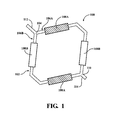
FIG. 1 is a schematic plan view of a wavepath unit cell;
FIG. 2A is a schematic plan view of a wavepath grid comprising a plurality of wavepath unit cells of the type illustrated in FIG. 1;
FIG. 2B is a calculated output power distribution curve for a wavepath grid of the type shown in FIG. 2A;
FIG. 2C is a plan view of the wavepath grid of FIG. 2A overlaying a size-descriptive grid;
FIG. 3A is a schematic plan view of a wavepath grid of the type shown in FIG. 2A and having a power splitting region;
FIG. 3B is a schematic plan view of a wavepath grid of the type shown in FIG. 3A and having a power splitting region and a power mixing region;
FIG. 4A is a two-dimensional graph of calculated output power distributions of wavepath grids of the type shown in FIG. 3B with power splitting regions of varying length;
FIG. 4B is a three-dimensional graph illustrating the data of FIG. 4A; and
FIG. 5 is a perspective view of a phased-array device having a wavepath grid of the type illustrated in FIG. 2A but with slightly different unit cell geometry.
DETAILED DESCRIPTION
The present disclosure describes a lightpath architecture for optical phased-array systems. An existing phased-array system splits a light source into multiple parallel channels, passes each channel through a variable phase shifter such as a medium of different refractive index, and then emits the various channels in close proximity to one another (on the order of 1 μm). Such a system allows the creation of an engineered wavefront, controlled by the pattern of interferences and coherences between the various, emitted, phase-shifted channels. This wavefront engineering can enable beam steering without moving parts, useful for example in a Lidar system, or tunable depth perception.
Previous phased-array systems may use a graded architecture wherein separate wavepath channels are equipped with different phase shift elements. For example, a linear distribution of phase shift element lengths can produce a linear distribution of output phases. Unfortunately, it can also produce an asymmetrical power distribution.
By contrast, phased array devices of the present disclosure utilize a wavepath grid with unit cell architecture to produce linear phase distribution with symmetrical power distribution. The disclosed architecture features a criss-crossing waveguide network with interspersed with phase shift elements of equal magnitude but opposite sign. The phase at any output point is controlled by the ratio of positive to negative phase shift elements encountered while the power is dictated by the ratio of convergence points to splitting points in the grid, as explained further below.
Referring now to FIG. 1, a wavepath unit cell 100 includes a waveguide 102 operable to direct the propagation of a wave. In some variations, waveguide 102 will be configured to direct the propagation of an electromagnetic wave. In some particular variations, waveguide 102 will be configured to direct the propagation of any or all of an infrared, visible, or ultraviolet electromagnetic wave. Waveguide 102 will typically comprise a rib waveguide or similar structure operable to direct propagation of a wave substantially in one direction at any point in the waveguide 102. Waveguide 102 can comprise any material suitable to guide propagation of the wave to be propagated. In many instances, waveguide 102 will comprise an optically active material, such as silicon.
Wavepath unit cell 100 can optionally include a waveguide inlet 104, operable to receive a coherent wave from a source and couple said coherent wave into waveguide 102. In some variations, a source of a coherent wave will be a laser. In some particular variations, a source of a coherent wave will be an infrared, visible, or ultraviolet laser. In general, the composition of waveguide 102 will be selected from suitable materials based on the nature and/or wavelength of the wave to be guided.
Wavepath unit cell 100 additionally includes a branch point 104 where waveguide 102 splits into two waveguide branches 106A and 106B. The wave directed into waveguide branch 106A and the wave directed into waveguide branch 106B will typically be of approximately equal amplitude, each approximately half that of the amplitude of the wave incident upon branch point 104.
Waveguide branch 106A directs the branched wave through two phase shift elements 108A and 108B in series. Phase shift elements 108A and 108B will each shift the phase of the coherent guided wave passing through them. The phase shift applied by phase shift elements 108A and 108B is substantially equivalent in magnitude, but opposite in sign relative to one another. Waveguide branch 106B also directs the branched wave through the two phase shift elements 108B and 108A, but in the opposite order relative to branch 106A. For ease of use, a phase shift element 108A may be referred to as a “positive phase shift element” and a phase shift element 108B may be referred to as a “negative phase shift element”, although the specific designation of “positive” and “negative” as used here is arbitrary.
Phase shift elements 108A, 108B can be prepared by any suitable means such as temperature modulation of waveguide 102 at the appropriate locations or by inclusion of materials having different inherent refractive index at the appropriate locations.
Wavepath unit cell 100 additionally includes a convergence point 110 where waveguide branches 106A and 106B meet and converge. A unit cell inlet portion 112 a unit cell outlet portion 114 are shown in the exemplary wavepath unit cell 100 of FIG. 1. In the example of FIG. 1, considered in isolation (i.e. not in combination with other unit cells) an entering wave such as a coherent infrared light wave enters waveguide 102 at waveguide inlet 104 and propagates substantially linearly toward branch point 104. At branch point 104, the input wave is split into two branch waves, one propagating through waveguide branch 106A and one propagating through waveguide branch 106B. The wave branch propagating through waveguide branch 106A first interacts with phase shift element 108A and experiences a phase shift of +θ then subsequently interacts with phase shift element 108B and experiences a phase shift of −θ. The wave branch propagating through waveguide branch 106B first interacts with phase shift element 108B and experiences a phase shift of −θ then subsequently interacts with phase shift element 108A and experiences a phase shift of +θ. The two branch waves are recombined at convergence point 110 to produce a coherent output wave propagating through waveguide continuation substantially identical to the input wave, aside from incidental power loss.
While the wavepath unit cell 100 as illustrated in FIG. 1 is hexagonal, this is but one example, and the shape or structure of the unit cell can be varied in any way which includes the aforementioned elements. It will generally be desirable however that the length of waveguide branches 106A and 106B between branch point 104 and convergence point 110 be the same.
Referring now to FIG. 2A, a wavepath grid 200 comprises a two-dimensional or three-dimensional array of unit cells of the type described above and illustrated in FIG. 1. As an example, the wavepath grid 200 of FIG. 2A comprises six complete unit cells 100A, 100B, 100C, 100D, 100E, and 100F, each of generally the same type as wavepath unit cell 100 shown in FIG. 1.
Individual unit cells 100A, 100B, 100C, 100D, 100E, and 100F generally have shared cell boundaries such that discrete portions of waveguide 102 simultaneously serve as different segments of adjacent unit cells. For example, and referring again to FIG. 2A, a single portion of waveguide 102 serves as the continuation branch 112 of unit cell 100A, as the inlet of unit cell 100E, as a section of waveguide branch 106B of unit cell 100C, and as a section of waveguide branch 106A of unit cell 100C.
Of importance, the various individual unit cells 100A, 100B, 100C, 100D, 100E, and 100F generally have the same orientation as one another. In particular, positive phase shift elements 108A are all in the same orientation relative to the immediately preceding branch point 104, as all negative phase shift elements 108B are uniformly in the opposite orientation.
Wavepath grid 200 can be characterized as having a primary inlet 204 and five terminal outlets 206A, 206B, 206C, 206D, and 206E which can be operable to emit the wave from the wavepath grid 200. Terminal outlets 206A, 206B, 206C, 206D, and 206E may also be referred to as output channels, and may include various structures such as a diffraction grating, which facilitate wave outcoupling from wavepath grid 200. As shown, the wave phases across terminal outlets 206A, 206B, 206C, 206D, and 206E differ according to a linear distribution. While the example of FIG. 2A has five terminal outlets, the wavepath grid 200 can, depending on its size, have any plurality of terminal outlets which can be operable to outcouple the wave.
As shown, the phases of waves arriving at terminal outlets 206A, 206B, 206C, 206D, or 206E have a linear distribution ranging uniformly from +4θ to −4θ. Notably, a wavepacket arriving at any one of terminal outlets 206A, 206B, 206C, 206D, or 206E must have passed through the same number of phase shift elements 108A, 108B. In the case of the wavepath grid 200 of FIG. 2A, any wave traveling from primary inlet 204 to any terminal outlet 206A, 206B, 206C, 206D, or 206E must pass through four phase shift elements 108A, 108B regardless of path taken. The ratio of positive phase shift elements 108A to negative phase shift elements 108B encountered differs for wave packets arriving at different terminal outlets, however. For example, a wave packet arriving at terminal outlet 206A will have passed through four positive phase shift elements 108A while a wave packet arriving at terminal outlet 206C will have passed through two positive phase shift elements 108A and two negative phase shift elements 108B. The differing ratios of positive phase shift elements 108A to negative phase shift elements 108B encountered on the paths to the different terminal outlets creates the linear phase distribution.
The power distribution of wavepath grid 200 does not correspond directly to the phase distribution. While, as mentioned, phase distribution arises from the ratio of positive to negative phase shift elements encountered on the paths to the various terminal outlets 206A, 206B, 206C, 206D, and 206E, the power distribution arises from the ratio of branch points 104 to convergence points 110 encountered on the paths to the various terminal outlets 206A, 206B, 206C, 206D, and 206E. FIG. 2B shows a calculated power distribution for the wavepath grid 200 of FIG. 2A. Terminal outlets 206A, 206B, 206C, 206D, and 206E correspond to output channels 1, 2, 3, 4, and 5, respectively. As shown, the power distribution somewhat approximates a normal distribution, with output power significantly concentrated toward the middle and away from the edges of the grid. As discussed below, the shape of the power distribution can be substantially modified by changing the size and shape of wavepath grid 200, but first a system for describing the size and shape of a wavepath grid 200 must be defined.
The wavepath grid 200 of the type described above and exemplified in FIG. 2 can include any number of unit cells arrayed in a wide variety of arrangements. Such variations of wavepath grid 200 can be described with reference to a Cartesian coordinate system, one example of which is shown in FIG. 2C. In FIG. 2C, the wavepath grid of FIG. 2A is shown overlaying a two-dimensional Cartesian coordinate system having (n) and (m) axes.
In the (n,m) coordinate system as shown, the (n) and (m) axes intersect adjacent to primary inlet point 204. Repeating structures of wavepath grid 200 appear at regular intervals on the (n, m) coordinate system. The wavepath grid 200 of FIGS. 2A and 2C can be described as a 2×2 grid. This is because, in this example, wavepath grid 200 crosses a maximum number of coordinate lines in the (n), exclusive of n=0, and crosses a maximum of two coordinate lines in the (m) direction, on either side of, and exclusive of, m=0. While a variety of different coordinate systems could be used to describe wavepath grid 200 size and shape, the present disclosure employs the (n, m) coordinate system as illustrated to describe the size and shape of different variations of wavepath grid 200. For ease of use, size of a wavepath grid 200 in the (n) dimension can at times be referred to as “length” while size in the (m) dimension can at times be referred to as “width”.
Additional variations in the number, and particularly the arrangement, of unit cells 100 employed in a wavepath grid 200 are illustrated in FIGS. 3A and 3B. FIG. 3A shows a wavepath grid 200 of dimension 4×4, while FIG. 3B shows a wavepath grid of dimension 8×4. The 4×4 grid phase shifting region 250. A phase shifting region 250 is a portion of a wavepath grid 200 is one in which higher numbered coordinate positions in the (n) direction correspond to a greater number of coordinate positions occupied in the (m) direction. Stated in general terms, length and width of the wavepath grid 250 simultaneously and proportionally increase in the phase shifting region 250.
The wavepath grid 200 of FIG. 3B includes the power splitting region 250 of FIG. 3A and then proceeds into a power mixing region 252, where higher numbered coordinate positions in the (n) direction do not correspond to a greater number of coordinate positions occupied in the (m) direction. In general terms, length of wavepath grid 200 increases in the power mixing region, but width does not. Such structural variations, such as inclusion of a power mixing region or varying the length of a power mixing region can have significant effects on the functional properties of a wavepath grid 200, such as on the output power distribution. In general functional terms, the phase shifting region 250 transforms a single input channel into a plurality of channels having linear phase distribution and power concentrated in the middle channels. The power mixing region 252 maintains the phase distribution created by the phase shifting region 250, while redistributing a portion of the power away from the middle channels.
FIG. 4A shows the calculated power distributions of wavepath grids 200 of varying arrangement. Each wavepath grid 200 assessed in FIG. 4A has an equivalent 16×16 power splitting region which then proceeds into a power mixing region of varying (n) dimension. For example, the 32×16 wavepath grid has a 16×16 power splitting region 250 proceeding into a power mixing region 252 increasing the length of the array by an additional 16 units in the (n) direction with no increase in the (m) direction. Each wavepath grid 200 has thirty-three output channels numbered sequentially similar to the five output channels of FIG. 2B. It is to be noted that the power mixing regions are greater in length than the power splitting regions for the 32×16, 48×16, 64×16, 128×16, and 256×16 wavepath grids.
As the calculated data from FIG. 4A show, the 16×16 wavepath grid has a power distribution heavily concentrated toward the middle output channels, i.e. those corresponding to lower values of |m|. However, as power mixing regions of greater length are included into the arrays, the power distribution becomes substantially broader. This is because the power mixing region 252 allows amplitude mixing across the width of the grid without the increasing channel dilution toward the edges that is created by the phase shifting region 250. The data from FIG. 4A is alternatively displayed in a three-dimensional graph in FIG. 4B, to greater illustrate the relationship between power mixing region length and power distribution broadening.
Referring now to FIG. 5, a phased-array device 300 includes a wavepath grid 200, of the type disclosed, arrayed on a chip 302. While phased-array device 300 can be of any type known in the art, it will typically be an optical phased-array device. While chip 302 can be of any suitable construction, it can in some cases of be of silicon-on-chip construction.
FIG. 5 shows one example of phased-array device 300, in which the chip 302 is of silicon-on-insulator construction. Phased-array device 300 includes wavepath grid 200, wherein waveguide 102 comprises a suitable material such as silicon contactingly overlaying an insulator layer 304. The wavepath grid 200 includes an array of wavepath unit cells as described above. Insulator layer 304 can comprise an oxide such as silicon oxide or other suitable oxide. Insulator 304 can in some instances contactingly overlay a substrate layer 306, such as may also comprise silicon. Wavepath grid 200 as employed in phased-array device 300 includes a plurality of terminal outlets such as are created by diffraction grating 308 that is etched into the phased-array device 300 to a depth sufficient to create wave outcoupling from waveguide 102. As above, the plurality of terminal outlets can be operable to outcouple individual sub-beams of the input wave from the chip.
The phased-array device 300 can additionally include at least one control channel operable to modulate the refractive index of positive phase shift elements 108A, negative phase shift elements 108B, or both. For example, the control channel could comprise a plurality of thermoelectric devices arrayed to simultaneously heat waveguide 102 at locations corresponding to positive phase shift elements 108A and to cool waveguide 102 at locations corresponding to negative phase shift elements 108B.
Alternatively, the control channel could comprise a plurality of heating elements arrayed to heat waveguide 102 at locations corresponding to positive and negative phase shift elements 108A and 108B. In such a scenario, negative phase shift elements 108B may comprise a material which has a higher index of refraction as compared to the material of which waveguide 102 and/or positive phase shift elements 108A are comprised.
In an alternative control system, the waveguide can be subject to a DC offset. In such a system, the entire waveguide including positive and negative phase-shift elements is comprised of a single material, such as silicon. The portions of waveguide 112 outside the positive and negative phase-shift elements has an applied voltage such as +0.5 V. The positive phase shift elements have an applied voltage of +1.0 V and the negative phase shift elements have no applied voltage. Thus the preponderance of the waveguide 112 is warmed somewhat, the positive phase-shift elements are warmed to a greater extent, and the negative phase-shift elements are not warmed.
A control channel of these types, or any other, can be used in conjunction with phased array device 300 to produce a beam steering device with no moving parts. For example, by modulating the magnitude of θ in positive phase shift elements 108A, in negative phase shift elements 108B, or both, the relative phases at the terminal outlets are altered. Consequently, the direction of propagation of the emitted beam is controllably steered.
A control channel of any of the types described, or another type, could be distributed within or upon a thermal layer contactingly overlaying and surrounding wavepath grid 200. For example, a control channel consisting substantially of a titanium or other conductive electrode could be sputtered on top of a layer of benzylcyclobutane (BCB), the BCB layer contactingly overlaying the waveguide and oxide layer.
The foregoing description relates to what are presently considered to be the most practical embodiments. It is to be understood, however, that the disclosure is not to be limited to these embodiments but, on the contrary, is intended to cover various modifications and equivalent arrangements included within the spirit and scope of the appended claims, which scope is to be accorded the broadest interpretation so as to encompass all such modifications and equivalent structures as is permitted under the law.

Claims (20)

What is claimed is:
1. A linear phased-array device comprising:
a chip;
a wavepath grid comprising a two-dimensional array of wavepath unit cells, each unit cell including;
a waveguide;
a branch point in the waveguide, the branch point leading to first and second waveguide branches; and
a convergence point of the first and second waveguide branches;
wherein the first waveguide branch passes first through a positive phase shift element and subsequently through a negative phase shift element and the second waveguide branch passes first through a negative phase shift element and subsequently through a positive phase shift element; and
a plurality of terminal outlets disposed within the wavepath grid and operable to outcouple individual sub-beams of a wave from the chip.
2. The device as recited in claim 1, which is operable to transmit an acoustic or electromagnetic wave.
3. The device as recited in claim 1, and which is operable to transmit an electromagnetic wave.
4. The device as recited in claim 1, and which is operable to transmit an optical wave.
5. The device as recited in claim 1, having a symmetrical output power distribution.
6. The device as recited in claim 1, wherein the waveguide consists essentially of silicon.
7. The device as recited in claim 1, wherein the chip comprises silicon-on-oxide.
8. The device as recited in claim 1, wherein the wavepath grid further comprises a power splitting region and a power mixing region.
9. The device as recited in claim 1, wherein plurality of terminal outlets comprise a diffraction grating.
10. The device as recited in claim 1, further comprising a single-channel control.
11. The device as recited in claim 1, further comprising a dual-channel control.
12. The device as recited in claim 1, wherein the dual-channel control comprises a DC-offset.
13. A wavepath grid comprising:
a two-dimensional array of wavepath unit cells, each unit cell including;
a waveguide;
a branch point in the waveguide, the branch point leading to first and second waveguide branches; and
a convergence point of the first and second waveguide branches;
wherein the first waveguide branch passes first through a positive phase shift element and subsequently through a negative phase shift element and the second waveguide branch passes first through a negative phase shift element and subsequently through a positive phase shift element, and wherein the wavepath grid is operable to receive a coherent wave source, to split the coherence wave source into multiple individual sub-beams, and to differentially shift the phase of each of the multiple individual sub-beams.
14. The wavepath grid as recited in claim 13, further comprising a power splitting region and a power mixing region.
15. The wavepath grid as recited in claim 14, wherein the power mixing region is greater in length than is the power splitting region.
16. The wavepath grid as recited in claim 13, wherein the coherent wave source comprises an acoustic or electromagnetic wave.
17. The wavepath grid as recited in claim 13, wherein the coherent wave source comprises a laser.
18. The wavepath grid as recited in claim 13, wherein the coherent wave source comprises an optical laser.
19. The wavepath grid as recited in claim 13, having a symmetrical output power distribution.
20. The wavepath grid as recited in claim 13, wherein the waveguide consists essentially of silicon.
US14/285,238 2014-05-22 2014-05-22 Unit cell based wavepath grid architecture applicable and to phased-array devices and enabling symmetrical output power distribution and single channel control Expired - Fee Related US9188740B1 (en)

Priority Applications (1)

Application Number Priority Date Filing Date Title
US14/285,238 US9188740B1 (en) 2014-05-22 2014-05-22 Unit cell based wavepath grid architecture applicable and to phased-array devices and enabling symmetrical output power distribution and single channel control

Applications Claiming Priority (1)

Application Number Priority Date Filing Date Title
US14/285,238 US9188740B1 (en) 2014-05-22 2014-05-22 Unit cell based wavepath grid architecture applicable and to phased-array devices and enabling symmetrical output power distribution and single channel control

Publications (2)

Publication Number Publication Date
US9188740B1 true US9188740B1 (en) 2015-11-17
US20150338576A1 US20150338576A1 (en) 2015-11-26

Family

ID=54434555

Family Applications (1)

Application Number Title Priority Date Filing Date
US14/285,238 Expired - Fee Related US9188740B1 (en) 2014-05-22 2014-05-22 Unit cell based wavepath grid architecture applicable and to phased-array devices and enabling symmetrical output power distribution and single channel control

Country Status (1)

Country Link
US (1) US9188740B1 (en)

Cited By (4)

* Cited by examiner, † Cited by third party
Publication number Priority date Publication date Assignee Title
TWI655843B (en) * 2018-06-25 2019-04-01 國立暨南國際大學 Multiple RF power amplifier
CN109901263A (en) * 2019-01-29 2019-06-18 浙江大学 A kind of silicon substrate integrated optics phased array chip based on common electrode
US20210382235A1 (en) * 2020-06-08 2021-12-09 Honeywell International Inc. Multilayer optical phased arrays for sidelobe mitigation
US11662511B2 (en) 2020-07-22 2023-05-30 Samsung Electronics Co., Ltd. Beam expander and method of operating the same

Families Citing this family (1)

* Cited by examiner, † Cited by third party
Publication number Priority date Publication date Assignee Title
KR102407142B1 (en) * 2017-06-30 2022-06-10 삼성전자주식회사 Beam steering device and electronic apparatus including the same

Citations (8)

* Cited by examiner, † Cited by third party
Publication number Priority date Publication date Assignee Title
US20020057866A1 (en) * 2000-10-16 2002-05-16 Henry Hung Apparatus for adding wavelength components in wavelength division mulitplexed optical signals using multiple wavelength sagnac interferometer switch
US6538787B1 (en) * 1999-09-24 2003-03-25 Lucent Technologies Inc. Apparatus and method for polarization mode dispersion emulation and compensation
US20030058504A1 (en) * 2000-09-26 2003-03-27 Cho Pak Shing Method and system for mitigating nonlinear transmission impairments in fiber-optic communications systems
WO2003079101A1 (en) 2002-03-15 2003-09-25 Universidad Politecnica De Valencia Beam-forming network for groups of antennae based on optical matrices of fixed phase-shift/delay elements
US20090003841A1 (en) * 2004-03-31 2009-01-01 Pirelli & C.S.P.A. Optical Modulator
US8380016B1 (en) * 2009-06-09 2013-02-19 University Of Washington Through Its Center For Commercialization Geometries for electrooptic modulation with χ2 materials in silicon waveguides
US8467641B2 (en) 2010-03-12 2013-06-18 The Johns Hopkins University System and method for using planar device to generate and steer light beam
WO2013123520A1 (en) 2012-02-16 2013-08-22 California Institute Of Technology Integrated two-dimensional planar optical phased array

Patent Citations (8)

* Cited by examiner, † Cited by third party
Publication number Priority date Publication date Assignee Title
US6538787B1 (en) * 1999-09-24 2003-03-25 Lucent Technologies Inc. Apparatus and method for polarization mode dispersion emulation and compensation
US20030058504A1 (en) * 2000-09-26 2003-03-27 Cho Pak Shing Method and system for mitigating nonlinear transmission impairments in fiber-optic communications systems
US20020057866A1 (en) * 2000-10-16 2002-05-16 Henry Hung Apparatus for adding wavelength components in wavelength division mulitplexed optical signals using multiple wavelength sagnac interferometer switch
WO2003079101A1 (en) 2002-03-15 2003-09-25 Universidad Politecnica De Valencia Beam-forming network for groups of antennae based on optical matrices of fixed phase-shift/delay elements
US20090003841A1 (en) * 2004-03-31 2009-01-01 Pirelli & C.S.P.A. Optical Modulator
US8380016B1 (en) * 2009-06-09 2013-02-19 University Of Washington Through Its Center For Commercialization Geometries for electrooptic modulation with χ2 materials in silicon waveguides
US8467641B2 (en) 2010-03-12 2013-06-18 The Johns Hopkins University System and method for using planar device to generate and steer light beam
WO2013123520A1 (en) 2012-02-16 2013-08-22 California Institute Of Technology Integrated two-dimensional planar optical phased array

Non-Patent Citations (2)

* Cited by examiner, † Cited by third party
Title
Doylend et al., "Two-dimensional free-space beam steering with an optical phased array on silicon-on-insulator" Oct. 24, 2011 / vol. 19, No. 22 / Optics Express 21595-21604.
Van Acoleyen et al., "Off-chip beam steering with a one-dimensional optical phased array on silicon-on-insulator" May 1, 2009 / vol. 34, No. 9 / Optics Letters, pp. 1477-1479.

Cited By (5)

* Cited by examiner, † Cited by third party
Publication number Priority date Publication date Assignee Title
TWI655843B (en) * 2018-06-25 2019-04-01 國立暨南國際大學 Multiple RF power amplifier
CN109901263A (en) * 2019-01-29 2019-06-18 浙江大学 A kind of silicon substrate integrated optics phased array chip based on common electrode
CN109901263B (en) * 2019-01-29 2021-01-08 浙江大学 Silicon-based integrated optical phased array chip based on common electrode
US20210382235A1 (en) * 2020-06-08 2021-12-09 Honeywell International Inc. Multilayer optical phased arrays for sidelobe mitigation
US11662511B2 (en) 2020-07-22 2023-05-30 Samsung Electronics Co., Ltd. Beam expander and method of operating the same

Also Published As

Publication number Publication date
US20150338576A1 (en) 2015-11-26

Similar Documents

Publication Publication Date Title
US9188740B1 (en) Unit cell based wavepath grid architecture applicable and to phased-array devices and enabling symmetrical output power distribution and single channel control
JP7138964B2 (en) Phase-controlled optical waveguide antenna array
EP3407128B1 (en) Light-deflecting device and lidar apparatus
US20170131615A1 (en) Photonic Phased Array Antenna
US9726818B1 (en) Multi-wavelength band optical phase and amplitude controller
US20190219888A1 (en) On-chip optical phased array using a serial grating antenna design
US11320717B2 (en) Optical phase array, methods of forming and operating the same
US20170307810A1 (en) Diffraction structure, diffraction grating, diffraction grating array, optical phased array, optical modulator, optical filter, laser source
US10634845B2 (en) Integrated planar optical phased array
US8467641B2 (en) System and method for using planar device to generate and steer light beam
US11422431B2 (en) Optical switching using spatially distributed phase shifters
CN109212506B (en) Beam steering device and light detection and ranging device
KR20180020035A (en) OPA(Optical Phased Array) for beam steering, and LiDAR(Light Detection And Ranging) system comprising the same OPA
KR102496484B1 (en) Light steering apparatus and system including the light steering apparatus
US9467755B2 (en) Optical switch
US20160266316A1 (en) Device for coupling a plurality of different fibre modes
US11307354B2 (en) Wavelength selective switch based on LCoS
KR20240021992A (en) Beam controller and beam control method
JP4327064B2 (en) Light control element
US6999639B2 (en) Tunable optical filters
Stanley et al. Mach–Zehnder interferometer: A review of a perfect all-optical switching structure
JP5926219B2 (en) Optical input / output device
JP2019184649A (en) Optical deflection element
Foster et al. Chip-scale optical phased arrays for inter-spacecraft communications
JP2009198826A (en) Optical signal processor

Legal Events

Date Code Title Description
AS Assignment

Owner name: TOYOTA MOTOR ENGINEERING & MANUFACTURING NORTH AME

Free format text: ASSIGNMENT OF ASSIGNORS INTEREST;ASSIGNOR:NOMURA, TSUYOSHI;REEL/FRAME:033044/0680

Effective date: 20140521

STCF Information on status: patent grant

Free format text: PATENTED CASE

AS Assignment

Owner name: KABUSHIKI KAISHA TOYOTA CHUO KENKYUSHO, JAPAN

Free format text: ASSIGNMENT OF ASSIGNORS INTEREST;ASSIGNOR:TOYOTA MOTOR ENGINEERING & MANUFACTURING NORTH AMERICA, INC.;REEL/FRAME:037078/0205

Effective date: 20151112

CC Certificate of correction
MAFP Maintenance fee payment

Free format text: PAYMENT OF MAINTENANCE FEE, 4TH YEAR, LARGE ENTITY (ORIGINAL EVENT CODE: M1551); ENTITY STATUS OF PATENT OWNER: LARGE ENTITY

Year of fee payment: 4

FEPP Fee payment procedure

Free format text: MAINTENANCE FEE REMINDER MAILED (ORIGINAL EVENT CODE: REM.); ENTITY STATUS OF PATENT OWNER: LARGE ENTITY

LAPS Lapse for failure to pay maintenance fees

Free format text: PATENT EXPIRED FOR FAILURE TO PAY MAINTENANCE FEES (ORIGINAL EVENT CODE: EXP.); ENTITY STATUS OF PATENT OWNER: LARGE ENTITY

STCH Information on status: patent discontinuation

Free format text: PATENT EXPIRED DUE TO NONPAYMENT OF MAINTENANCE FEES UNDER 37 CFR 1.362

FP Lapsed due to failure to pay maintenance fee

Effective date: 20231117