US9202702B2 - Semiconductor device having at least one contact, and manufacturing method for a semiconductor device having at least one contact - Google Patents

Semiconductor device having at least one contact, and manufacturing method for a semiconductor device having at least one contact Download PDF

Info

Publication number
US9202702B2
US9202702B2 US13/446,531 US201213446531A US9202702B2 US 9202702 B2 US9202702 B2 US 9202702B2 US 201213446531 A US201213446531 A US 201213446531A US 9202702 B2 US9202702 B2 US 9202702B2
Authority
US
United States
Prior art keywords
layer
lift
contact
conforming
substrate
Prior art date
Legal status (The legal status is an assumption and is not a legal conclusion. Google has not performed a legal analysis and makes no representation as to the accuracy of the status listed.)
Expired - Fee Related, expires
Application number
US13/446,531
Other versions
US20120292641A1 (en
Inventor
Frederik Schrey
Achim Trautmann
Joachim Rudhard
Current Assignee (The listed assignees may be inaccurate. Google has not performed a legal analysis and makes no representation or warranty as to the accuracy of the list.)
Robert Bosch GmbH
Original Assignee
Robert Bosch GmbH
Priority date (The priority date is an assumption and is not a legal conclusion. Google has not performed a legal analysis and makes no representation as to the accuracy of the date listed.)
Filing date
Publication date
Application filed by Robert Bosch GmbH filed Critical Robert Bosch GmbH
Assigned to ROBERT BOSCH GMBH reassignment ROBERT BOSCH GMBH ASSIGNMENT OF ASSIGNORS INTEREST (SEE DOCUMENT FOR DETAILS). Assignors: SCHREY, FREDERIK, TRAUTMANN, ACHIM, RUDHARD, JOACHIM
Publication of US20120292641A1 publication Critical patent/US20120292641A1/en
Application granted granted Critical
Publication of US9202702B2 publication Critical patent/US9202702B2/en
Expired - Fee Related legal-status Critical Current
Adjusted expiration legal-status Critical

Links

Images

Classifications

    • HELECTRICITY
    • H01ELECTRIC ELEMENTS
    • H01LSEMICONDUCTOR DEVICES NOT COVERED BY CLASS H10
    • H01L21/00Processes or apparatus adapted for the manufacture or treatment of semiconductor or solid state devices or of parts thereof
    • H01L21/02Manufacture or treatment of semiconductor devices or of parts thereof
    • H01L21/04Manufacture or treatment of semiconductor devices or of parts thereof the devices having at least one potential-jump barrier or surface barrier, e.g. PN junction, depletion layer or carrier concentration layer
    • H01L21/18Manufacture or treatment of semiconductor devices or of parts thereof the devices having at least one potential-jump barrier or surface barrier, e.g. PN junction, depletion layer or carrier concentration layer the devices having semiconductor bodies comprising elements of Group IV of the Periodic System or AIIIBV compounds with or without impurities, e.g. doping materials
    • H01L21/28Manufacture of electrodes on semiconductor bodies using processes or apparatus not provided for in groups H01L21/20 - H01L21/268
    • H01L21/283Deposition of conductive or insulating materials for electrodes conducting electric current
    • H01L21/285Deposition of conductive or insulating materials for electrodes conducting electric current from a gas or vapour, e.g. condensation
    • H01L21/28506Deposition of conductive or insulating materials for electrodes conducting electric current from a gas or vapour, e.g. condensation of conductive layers
    • HELECTRICITY
    • H01ELECTRIC ELEMENTS
    • H01LSEMICONDUCTOR DEVICES NOT COVERED BY CLASS H10
    • H01L21/00Processes or apparatus adapted for the manufacture or treatment of semiconductor or solid state devices or of parts thereof
    • H01L21/70Manufacture or treatment of devices consisting of a plurality of solid state components formed in or on a common substrate or of parts thereof; Manufacture of integrated circuit devices or of parts thereof
    • H01L21/71Manufacture of specific parts of devices defined in group H01L21/70
    • H01L21/768Applying interconnections to be used for carrying current between separate components within a device comprising conductors and dielectrics
    • H01L21/76838Applying interconnections to be used for carrying current between separate components within a device comprising conductors and dielectrics characterised by the formation and the after-treatment of the conductors
    • H01L21/76877Filling of holes, grooves or trenches, e.g. vias, with conductive material
    • H01L21/7688Filling of holes, grooves or trenches, e.g. vias, with conductive material by deposition over sacrificial masking layer, e.g. lift-off
    • HELECTRICITY
    • H01ELECTRIC ELEMENTS
    • H01LSEMICONDUCTOR DEVICES NOT COVERED BY CLASS H10
    • H01L21/00Processes or apparatus adapted for the manufacture or treatment of semiconductor or solid state devices or of parts thereof
    • H01L21/02Manufacture or treatment of semiconductor devices or of parts thereof
    • H01L21/04Manufacture or treatment of semiconductor devices or of parts thereof the devices having at least one potential-jump barrier or surface barrier, e.g. PN junction, depletion layer or carrier concentration layer
    • H01L21/0445Manufacture or treatment of semiconductor devices or of parts thereof the devices having at least one potential-jump barrier or surface barrier, e.g. PN junction, depletion layer or carrier concentration layer the devices having semiconductor bodies comprising crystalline silicon carbide
    • H01L21/048Making electrodes
    • HELECTRICITY
    • H01ELECTRIC ELEMENTS
    • H01LSEMICONDUCTOR DEVICES NOT COVERED BY CLASS H10
    • H01L29/00Semiconductor devices adapted for rectifying, amplifying, oscillating or switching, or capacitors or resistors with at least one potential-jump barrier or surface barrier, e.g. PN junction depletion layer or carrier concentration layer; Details of semiconductor bodies or of electrodes thereof  ; Multistep manufacturing processes therefor
    • H01L29/02Semiconductor bodies ; Multistep manufacturing processes therefor
    • H01L29/12Semiconductor bodies ; Multistep manufacturing processes therefor characterised by the materials of which they are formed
    • H01L29/16Semiconductor bodies ; Multistep manufacturing processes therefor characterised by the materials of which they are formed including, apart from doping materials or other impurities, only elements of Group IV of the Periodic System
    • H01L29/1608Silicon carbide

Definitions

  • the present invention relates to a semiconductor device having at least one contact. Moreover, the present invention relates to a manufacturing method for a semiconductor device having at least one contact.
  • a method for structuring tungsten layers is described in German Patent No. DE 692 28 044 T2.
  • a mask made of titanium is formed.
  • a titanium layer is deposited on a structured lacquer layer which partially covers a tungsten layer.
  • the titanium deposited on the structured lacquer layer is washed off by removing the structured lacquer layer, using an acetone solvent spray mist. After etching the tungsten layer, using the mask made of titanium, the titanium mask may also be removed.
  • the present invention provides a semiconductor device, and a manufacturing method for a semiconductor device having at least one contact.
  • the present invention allows a novel metal structuring.
  • a conforming layer made of a conductive material which includes at least one metal is also advantageously structurable by using a lift-off process.
  • the lift-off process it is thus possible to structure out not only a mask composed of a nonconforming layer, but also a functional layer, as at least a part of a contact, from a conforming layer made of a conductive material which includes at least one metal.
  • at least one layer of a contact is also producible from a conductive material which contains at least one metal which is diffusible into the substrate material, without the risk of undesirable diffusion of the metal into the substrate material.
  • the present invention in particular allows a lift-off process to be carried out without the disadvantages often associated with this process.
  • the acceptability of the lift-off process for fabrication lines may be increased with the aid of the present invention.
  • a direct structuring process (composed of a lithographic step and a subsequent wet chemical or plasma-based structuring step) may be replaced. Since undesirable diffusion of a metal of the structured layer, in particular in the case of a structured nickel layer, frequently occurs in this type of direct structuring process, this disadvantage may be avoided via the present invention.
  • the technology according to the present invention eliminates the shortcomings of a lift-off process having only one negative resist step, as well as of direct structuring using only one resist mask applied to the layer to be structured.
  • the present invention allows formation of a stable electrical contact with the aid of a double-layer lift-off.
  • the yield and reliability of manufactured electrical contacts may be increased using this manufacturing method.
  • the manufacturable components are also suited for high-temperature processes due to the prevention of diffusion of metal contaminants.
  • the present invention may be used in particular in silicon carbide (SiC) technology, but is not limited to same.
  • the layer formed on the surface of the substrate is alloyed into a semiconductor material of the substrate. A more stable conductive contact across the layer is achievable in this way.
  • the layer may advantageously be made of nickel, a metal-nickel alloy, or an aluminum-cobalt alloy as the conductive material.
  • the layer is also producible from the named materials, which usually are not suitable for forming a layer as at least a part of a contact using a sputtering process and/or a lift-off process.
  • outer base area and/or the outer contact area may be free of tear-off marks. These areas may thus be formed with a smooth outer surface.
  • the substrate may preferably include silicon carbide. It is thus possible to make use of the advantages of SiC technology for the semiconductor device.
  • the at least one layer may have a first extension in a first spatial direction, oriented parallel to the surface, which is identical to a second extension along a second spatial direction, perpendicular to the first spatial direction, oriented parallel to the surface.
  • This type of contact has a relatively large attack surface for a lift-off process step, and is therefore reliably producible in this way.
  • the at least one layer may have a design which is meander-shaped, zigzag-shaped, and/or offset in sections in a surface that is oriented parallel to the surface.
  • the at least one outer side area has edges or steps which provide advantageous tear-off options.
  • the conforming layer made of the conductive material is sputtered on.
  • a metal layer formed with the aid of a sputtering process has a more conforming design.
  • the sputtered-on metal layer achieves the characteristics of a conforming layer better than does a vapor-deposited metal layer.
  • the contacts formed from a sputtered-on metal layer are considerably more stable and reliable than contacts structured from a vapor-deposited metal layer. With the aid of the technology according to the present invention, it is also ensured that even a lift-off layer that is covered by the sputtered-on layer may be reliably removed.
  • the lift-off layer and/or mask may be formed from a photoresist. This allows simple removal of the lift-off layer and the mask with the aid of a lift-off process.
  • the at least one layer may be formed on the surface of the substrate and alloyed into a semiconductor material of the substrate with the aid of a heat treatment step. A good conductive contact over the at least one layer is achievable in this way.
  • the conforming layer may preferably be made of nickel, a metal-nickel alloy, or an aluminum-cobalt alloy as the conductive material.
  • the method may thus also be carried out using conductive materials which are not usable in a conventional manufacturing method using a lift-off process.
  • tear-off marks are formed on at least one outer side area between an outer base area facing the surface and an outer contact area facing away from the surface during removal of the lift-off layer by tearing away the residual area remaining after the etching process.
  • the at least one layer may thus be easily implemented in a desired small size.
  • the at least one continuous recess in the lift-off layer may be formed by a first extension in a first spatial direction oriented parallel to the surface, which is identical to a second extension along a second spatial direction, perpendicular to the first spatial direction, oriented parallel to the surface.
  • the at least one continuous recess in the lift-off layer may have a framing surface which is meander-shaped, zigzag-shaped, and/or offset in sections. It may thus be reliably ensured that the material introduced into the at least one recess has edges and/or steps for tear-off options.
  • FIGS. 1A through 1H show cross sections of a substrate for illustrating one specific example embodiment of the manufacturing method.
  • FIGS. 2A and 2B show schematic illustrations of two specific example embodiments of the semiconductor device.
  • FIGS. 1A through 1H show cross sections of a substrate for illustrating one specific embodiment of the manufacturing method.
  • the manufacturing method schematically represented with reference to FIGS. 1A through 1H may be carried out using a substrate 10 which includes a semiconductor material.
  • substrate 10 may in particular be made of the semiconductor material, for example silicon or silicon carbide.
  • the practicability of the method is not limited to the use of this type of substrate 10 .
  • a (functional) layer substructure may be provided in substrate 10 .
  • a (functional) layer substructure is a MOSFET in a substrate 10 made of silicon carbide.
  • the practicability of the method is not limited to a specific preparation/preprocessing of substrate 10 .
  • Insulating layer 14 is optionally applied on and/or above a surface 12 of substrate 10 . However, the method described below may also be carried out without forming insulating layer 14 .
  • Insulating layer 14 may be a silicon oxide layer, for example. However, another insulating material may also be used for forming insulating layer 14 .
  • Insulating layer 14 is preferably structured in such a way that at least one surface 22 is exposed, via a continuous recess 18 in insulating layer 14 , at least one position 16 of the contact to be subsequently formed. The at least one position 16 may also be understood to mean a target area of the contact to be subsequently formed, i.e., a (subsequent) contact area of substrate 10 .
  • FIG. 1A shows a cross section of the substrate after carrying out the above-described method steps.
  • the at least one continuous recess 18 in insulating layer 14 is formed, having a first extension a 01 in a first spatial direction 20 oriented parallel to surface 12 , which is identical to a second extension (not illustrated) along a second spatial direction, perpendicular to first spatial direction 20 , oriented parallel to surface 12 (not illustrated).
  • the at least one continuous recess 18 in insulating layer 14 may be formed in such a way that it frames a surface 22 which is meander-shaped, zigzag-shaped, and/or offset in sections.
  • some recesses 18 in insulating layer 14 may frame a surface 22 which is meander-shaped, zigzag-shaped, and/or offset in sections, while other continuous recesses have identical extensions along first spatial direction 20 and the second spatial direction which are oriented perpendicularly to one another.
  • the advantages of this type of design of the at least one continuous recess 18 in insulating layer 14 are described in greater detail below.
  • a lift-off layer 24 is formed on and/or above surface 12 of substrate 10 in another method step, a continuous recess 26 in lift-off layer 24 being formed at the at least one position 16 of the at least one contact to be formed.
  • the at least one continuous recess 26 opens up at least one surface 23 of a layer situated beneath lift-off layer 24 and/or surface 12 of substrate 10 at the at least one position.
  • inner wall surfaces 25 which are oriented (practically) perpendicularly with respect to surface 12 are provided at structured lift-off layer 24 which frame the at least one surface 23 of the layer and/or surface 12 of substrate 10 situated beneath lift-off layer 24 at the at least one position.
  • a photoresist layer is preferably formed as lift-off layer 24 .
  • the boundaries of the subsequently formed contact may be predefined with the aid of lift-off layer 24 .
  • FIG. 1B shows a cross section of substrate 10 after structured lift-off layer 24 is formed.
  • the at least one continuous recess 26 in lift-off layer 24 is preferably formed having a first extensional in first spatial direction 20 , which is identical to a second extension (not illustrated) in second spatial direction 20 (not illustrated).
  • the at least one continuous recess 26 in lift-off layer 24 may open up a surface 23 , which is meander-shaped, zigzag-shaped, and/or offset in sections, of the layer situated beneath lift-off layer 24 and/or surface 12 of substrate 10 . Combinations of these advantageous recesses 26 are also advantageous, as explained in greater detail below.
  • conforming layer 28 may be deposited over the entire surface, which may be easily carried out.
  • Conforming layer 28 may be formed having a (preferably practically uniform) layer thickness d, which corresponds to a thickness of the at least one contact to be formed perpendicularly to surface 12 of substrate 10 .
  • the layer of the contact is subsequently structured from the material which is deposited in the at least one position 16 , i.e., which covers at least one surface 23 which is framed by inner wall surfaces 25 .
  • Conforming layer 28 made of the conductive material is preferably sputtered on. This ensures the desired conformity of conforming layer 28 for a contact which is formable from same.
  • Conforming layer 28 may be made of nickel, a metal-nickel alloy, or an aluminum-cobalt alloy as the conductive material.
  • Conforming layer 28 is preferably made of titanium-nickel. However, the designability of conforming layer 28 is not limited to the materials listed here.
  • lift-off layer 24 protects the areas covered by same from inadvertent direct contact with the material of conforming layer 28 , in particular from inadvertent coating/covering by conforming layer 28 .
  • lift-off layer 24 ensures that the areas which it covers are reliably protected from diffusion of the at least one metal of conforming layer 28 . In this way, insulation areas which are covered by lift-off layer 24 are also reliably protected from diffusion of the at least one metal of conforming layer 28 , and thus, from contamination.
  • lift-off layer 24 prevents the metal of conforming layer 28 from contacting areas outside the at least one position 16 , i.e., the at least one desired contact area.
  • FIGS. 1D and 1E show cross sections of substrate 10 after at least one area 30 of conforming layer 28 , which is situated in the at least one position 16 /which covers at least one surface 23 framed by inner wall surfaces 25 , has been covered by a mask 32 .
  • Mask 32 is formed with at least one continuous recess above a residual area 34 of conforming layer 28 situated externally from the at least one position.
  • mask 32 may be formed in such a way that it has a clearance through residual area 34 as at least one continuous recess.
  • the at least one continuous recess of mask 32 may subdivide the mask into separate subareas which are situated above the at least two positions 16 /above the at least two surfaces 23 .
  • the subareas separated from each other preferably have a side edge 33 which is situated close to the edges of the associated position, i.e., close to inner wall surfaces 25 .
  • the structuring of mask 32 forms small “plaque-shaped” areas as mask 32 .
  • Mask 32 is preferably formed from a photoresist.
  • Mask 32 may be formed in such a way, for example, that the at least one side edge 33 is provided above the at least one inner wall surface 15 of insulating layer 14 (see FIG. 1D ).
  • the same exposure mask may be used for structuring lift-off layer 24 and mask 32 , lift-off layer 24 being formed from a “positive resist” and mask 32 being formed from a “negative resist.”
  • the method may also be referred to as a negative resist process.
  • the same exposure mask may be exposed, using modified exposure parameters, for structuring lift-off layer 24 and mask 32 .
  • mask 32 may be designed in such a way that the at least one side edge 33 is provided above the at least one inner wall surface 25 of lift-off layer 24 or above surface 23 framed by the at least one inner wall surface 25 (see FIG. 1E ).
  • an exposure mask which is different from the one used for structuring lift-off layer 24 is used for structuring mask 32 . This allows a more specific design of mask 32 with respect to the predefinable requirements, as is apparent from FIG. 1E .
  • FIG. 1F shows a cross section of substrate 10 after carrying out an etching process using mask 32 .
  • residual area 34 of conforming layer 28 which is not covered by mask 32 is at least partially etched away.
  • preferably only area 30 of conforming layer 28 protected by mask 32 remains at least partially in or above the at least one position 16 . It is thus possible to obtain attack surfaces for carrying out a lift-off process despite the conforming design of conforming layer 28 .
  • a solution used for the lift-off process is able to penetrate into the area between the remainder of conforming layer 28 and lift-off layer 24 , and thus detach lift-off layer 24 from the material which it covers.
  • the etching process may be a wet or dry chemical etching process, for example.
  • the etching solution used for the etching process is selective with respect to the conductive material of conforming layer 28 .
  • mask 32 and the lift-off layer are slightly etched by the etching solution or not at all.
  • the practicability of the etching process is not limited to a specific etching material.
  • Lift-off layer 24 also protects the areas underneath it during the etching of conforming layer 28 . If partial residues of conforming layer 28 remain on the surface of the etched areas, these partial residues are situated on the lift-off layer. Thus, during the etching process there is no risk of metal residues of conforming layer 28 diffusing into an area to be protected. In particular oxide areas, such as a gate oxide area in or on substrate 10 , are protected by lift-off layer 24 and therefore remain free of metal residues. The formation of metal silicide in polysilicon, which typically occurs during etching due to contamination by metal residues, is likewise prevented by lift-off layer 24 .
  • a lift-off process is carried out after the etching process.
  • lift-off layer 24 is removed, and the at least one layer 36 (as at least part of the contact) in the at least one position 16 is structured from the residue of conforming layer 28 which remains after the etching process.
  • the result is shown in FIG. 1G .
  • Acetone may be used, for example, to tear off lift-off layer 24 .
  • the practicability of the lift-off process described here is not limited to the use of acetone.
  • This method step may be reliably carried out due to the previously described advantageous formation of attack surfaces for a solution used in the lift-off process.
  • the solution is able to penetrate into the intermediate area, situated close to surface 23 , between the remainder of conforming layer 28 and lift-off layer 24 , which achieves good removability of lift-off layer 24 from the material which it covers.
  • the lift-off process may be carried out in such a way that tear-off marks are formed on at least one outer side area 40 between an outer base area 42 facing surface 12 and an outer contact area 44 facing away from surface 12 by tearing away material from (the remaining residue of) conforming layer 28 .
  • the tear-off marks result when lift-off layer 24 is removed by tearing away the material of conforming layer 28 adhering to same.
  • a layer 36 of a contact/a contact made of metal is produced for a defined contact area by forming the at least one layer 36 in the at least one position 16 .
  • An ohmic contact for example, is achieved with the aid of formed layer 36 .
  • the usability of layer 36 is not limited to use as an ohmic contact.
  • the at least one layer 36 may be easily formed in an advantageous small size with the aid of the above-described method steps.
  • Insulating layer 14 remains free of metal residues, even after lift-off layer 24 which previously covered it has been removed. Thus, there is no concern that a metal remaining on the insulating layer may diffuse into substrate 10 in a further method step.
  • the risk of diffusion of metal residues into the substrate is negligible, in particular also during a subsequent heat treatment step, for example a rapid thermal annealing (RTA) process for thermal activation.
  • RTA rapid thermal annealing
  • This type of heat treatment step may thus be easily carried out after the lift-off process.
  • a cleaning process may also optionally be carried out after the lift-off process.
  • the at least one layer 36 situated on the surface of substrate 10 is preferably alloyed into a semiconductor material of substrate 10 with the aid of a heat treatment step.
  • a suitable heat treatment step for this purpose are a rapid thermal annealing (RTA) process or a contact annealing step which may be carried out at a temperature above 1000° C., for example.
  • RTA rapid thermal annealing
  • a contact annealing step which may be carried out at a temperature above 1000° C., for example.
  • a different temperature may also be set for carrying out the heat treatment step.
  • the result of the heat treatment step is shown in FIG. 1H .
  • Layer 36 is preferably shaped and/or stabilized in the heat treatment step, which may also be referred to as a tempering process. Diffusion of metal outside the at least one position 16 is avoided due to the prevention of metal residues which has previously been carried out. Therefore, the heat treatment process is not limited with respect to temperature or time. The heat treatment process may typically have an overall process time of several minutes at temperatures around 1000° C. without concern for diffusion by metal.
  • semiconductor structures for example a MOSFET design having a gate oxide situated on or in substrate 10 , situated adjacent to the at least one position 16 , are covered by lift-off layer 24 in particular during the application and etching of conforming layer 28 .
  • lift-off layer 24 there is no concern that metal residues from conforming layer 28 will reach these structures.
  • a gate oxide or a gate oxide covered with a polysilicon layer may also be protected in such a way that its continued reliability is ensured.
  • metal residues such as nickel residues in particular, may be prevented from diffusing into the structures and/or substrate 10 situated therebeneath. Furthermore, the formation of an undesirable metal silicide is prevented in this way.
  • FIGS. 2A and 2B show schematic illustrations of two specific embodiments of the semiconductor device.
  • the semiconductor devices schematically represented in FIGS. 2A and 2B include a substrate 10 and at least one contact, situated on or above a surface 12 of substrate 10 , having at least one layer 36 made of a conductive material.
  • the conductive material includes at least one metal.
  • layer 36 may be made of nickel, a metal-nickel alloy, or an aluminum-cobalt alloy as the conductive material.
  • Layer 36 is preferably made of titanium-nickel.
  • the contact may have at least one further layer in addition to layer 36 described here.
  • Layer 36 made of the conductive material is sputtered on at or above surface 12 .
  • the type of metal deposition may be deduced by an analysis of the metal structure of layer 36 .
  • layer 36 has tear-off marks on at least one outer side area 40 between an outer base area 42 facing surface 12 and an outer contact area 44 facing away from surface 12 . It is thus apparent that layer 36 is structured from a sputtered-on, conforming layer via a lift-off process. While the at least one outer side area 40 has tear-off marks, the outer base area and/or outer contact area 44 is/are preferably free of tear-off marks.
  • the at least one contact/the at least one layer 36 may be formed using the above-described manufacturing method. However, the producibility of the at least one contact/the at least one layer 36 of the semiconductor devices in FIGS. 2A and 2B is not limited to strict adherence to the above-described method.
  • Layer 36 formed on surface 12 of substrate 10 is preferably alloyed into a semiconductor material of the substrate.
  • the semiconductor material of substrate 10 may be silicon carbide, for example.
  • the semiconductor device schematically represented in FIG. 2A has a layer 36 which is offset in sections in a surface oriented parallel to surface 12 .
  • the design of layer 36 may also be described in such a way that layer 36 is composed of first subareas 50 which extend along a first axis 52 , and second subareas 56 which extend along a second axis 54 which is parallel to first axis 52 .
  • a gap is present between two adjacent first subareas 50 .
  • a gap is also provided between two adjacent second subareas 56 .
  • the distance between first axis 52 and second axis 54 corresponds to the sum of the lateral distances of the mutually facing sides of subareas 50 and 56 from axes 52 and 54 , respectively.
  • the respective gap widths are set to be smaller than the extensions of subareas 50 and 56 in such a way that in each case an end of a first subarea 50 facing an adjacent first subarea 50 (laterally) contacts a second subarea 56 , while in each case an end of a second subarea 56 facing an adjacent second subarea 56 (laterally) contacts a first subarea 50 .
  • layer 36 is not limited to a design that is offset in sections.
  • the at least one layer 36 in the surface oriented parallel to surface 12 may also be meander-shaped or zigzag-shaped.
  • layer 36 Due to the advantageous design of layer 36 , this layer has a large number of edges or steps in relation to its volume. In addition, layer 36 has a comparatively large overall surface area of the at least one outer side area 40 in relation to its volume. Layer 36 thus provides good tear-off options which allow the lift-off process to be reliably carried out.
  • the semiconductor device schematically represented in FIG. 2B has multiple layers 36 , each having a first extensional in a first spatial direction 20 oriented parallel to surface 12 , which is identical to a second extension a 2 along a second spatial direction 60 , perpendicular to first spatial direction 20 , oriented parallel to surface 12 . This ensures the advantages listed in the description of FIG. 2A .
  • the lift-off process may be simplified with the aid of the above-described examples of an advantageous design modification.
  • structures having a square surface area those that are meander-shaped, zigzag-shaped, or are offset in sections have improved suppression of metal residues at edges of the lift-off layer. Metal residues are not expected to be a problem for the two described design modifications.

Abstract

A semiconductor device having a substrate, and at least one contact, situated on and/or above a surface of the substrate, having at least one layer made of a conductive material, the conductive material including at least one metal. The layer made of the conductive material is sputtered on, and has tear-off marks on at least one outer side area between an outer base area facing the surface and an outer contact area facing away from the surface. A manufacturing method for a semiconductor device having at least one contact is also described.

Description

CROSS REFERENCE
The present application claims the benefit under 35 U.S.C. §119 of German Patent Application No. DE 102011075888.7 filed on May 16, 2011, which is expressly incorporated herein by reference in its entirety.
FIELD OF THE INVENTION
The present invention relates to a semiconductor device having at least one contact. Moreover, the present invention relates to a manufacturing method for a semiconductor device having at least one contact.
BACKGROUND INFORMATION
A method for structuring tungsten layers is described in German Patent No. DE 692 28 044 T2. In the method, a mask made of titanium is formed. For this purpose, a titanium layer is deposited on a structured lacquer layer which partially covers a tungsten layer. In a subsequent lift-off process, the titanium deposited on the structured lacquer layer is washed off by removing the structured lacquer layer, using an acetone solvent spray mist. After etching the tungsten layer, using the mask made of titanium, the titanium mask may also be removed.
SUMMARY
The present invention provides a semiconductor device, and a manufacturing method for a semiconductor device having at least one contact.
The present invention allows a novel metal structuring. With the aid of the present invention, a conforming layer made of a conductive material which includes at least one metal is also advantageously structurable by using a lift-off process. With the aid of the lift-off process, it is thus possible to structure out not only a mask composed of a nonconforming layer, but also a functional layer, as at least a part of a contact, from a conforming layer made of a conductive material which includes at least one metal. At the same time, with the aid of the present invention, at least one layer of a contact is also producible from a conductive material which contains at least one metal which is diffusible into the substrate material, without the risk of undesirable diffusion of the metal into the substrate material.
The present invention in particular allows a lift-off process to be carried out without the disadvantages often associated with this process. Thus, the acceptability of the lift-off process for fabrication lines may be increased with the aid of the present invention. In particular, with the aid of the present invention, a direct structuring process (composed of a lithographic step and a subsequent wet chemical or plasma-based structuring step) may be replaced. Since undesirable diffusion of a metal of the structured layer, in particular in the case of a structured nickel layer, frequently occurs in this type of direct structuring process, this disadvantage may be avoided via the present invention.
Metal residues are reliably prevented when the present invention is implemented. Thus, the technology according to the present invention eliminates the shortcomings of a lift-off process having only one negative resist step, as well as of direct structuring using only one resist mask applied to the layer to be structured.
The present invention allows formation of a stable electrical contact with the aid of a double-layer lift-off. The yield and reliability of manufactured electrical contacts may be increased using this manufacturing method. The manufacturable components are also suited for high-temperature processes due to the prevention of diffusion of metal contaminants.
The present invention may be used in particular in silicon carbide (SiC) technology, but is not limited to same.
In one advantageous specific embodiment, the layer formed on the surface of the substrate is alloyed into a semiconductor material of the substrate. A more stable conductive contact across the layer is achievable in this way.
The layer may advantageously be made of nickel, a metal-nickel alloy, or an aluminum-cobalt alloy as the conductive material. With the aid of the technology according to the present invention, the layer is also producible from the named materials, which usually are not suitable for forming a layer as at least a part of a contact using a sputtering process and/or a lift-off process.
In particular, the outer base area and/or the outer contact area may be free of tear-off marks. These areas may thus be formed with a smooth outer surface.
The substrate may preferably include silicon carbide. It is thus possible to make use of the advantages of SiC technology for the semiconductor device.
In another advantageous specific embodiment, the at least one layer may have a first extension in a first spatial direction, oriented parallel to the surface, which is identical to a second extension along a second spatial direction, perpendicular to the first spatial direction, oriented parallel to the surface. This type of contact has a relatively large attack surface for a lift-off process step, and is therefore reliably producible in this way.
As an alternative or in addition to this specific embodiment, the at least one layer may have a design which is meander-shaped, zigzag-shaped, and/or offset in sections in a surface that is oriented parallel to the surface. In this case as well, the at least one outer side area has edges or steps which provide advantageous tear-off options.
The above-described advantages are also ensured for a corresponding manufacturing method for a semiconductor device.
In one advantageous specific embodiment of the method, the conforming layer made of the conductive material is sputtered on. Compared to a vapor-deposited metal layer, a metal layer formed with the aid of a sputtering process has a more conforming design. In other words, the sputtered-on metal layer achieves the characteristics of a conforming layer better than does a vapor-deposited metal layer. The contacts formed from a sputtered-on metal layer are considerably more stable and reliable than contacts structured from a vapor-deposited metal layer. With the aid of the technology according to the present invention, it is also ensured that even a lift-off layer that is covered by the sputtered-on layer may be reliably removed. Thus, due to the conforming design of a sputtered-on layer it is not necessary to dispense with a lift-off process. Likewise, it is not necessary to structure a vapor-deposited layer instead of a more advantageous sputtered-on layer to be able to satisfactorily carry out the lift-off process.
For example, the lift-off layer and/or mask may be formed from a photoresist. This allows simple removal of the lift-off layer and the mask with the aid of a lift-off process.
In addition, the at least one layer may be formed on the surface of the substrate and alloyed into a semiconductor material of the substrate with the aid of a heat treatment step. A good conductive contact over the at least one layer is achievable in this way.
The conforming layer may preferably be made of nickel, a metal-nickel alloy, or an aluminum-cobalt alloy as the conductive material. The method may thus also be carried out using conductive materials which are not usable in a conventional manufacturing method using a lift-off process.
In one advantageous specific embodiment, during the lift-off process, tear-off marks are formed on at least one outer side area between an outer base area facing the surface and an outer contact area facing away from the surface during removal of the lift-off layer by tearing away the residual area remaining after the etching process. The at least one layer may thus be easily implemented in a desired small size.
The at least one continuous recess in the lift-off layer may be formed by a first extension in a first spatial direction oriented parallel to the surface, which is identical to a second extension along a second spatial direction, perpendicular to the first spatial direction, oriented parallel to the surface. Alternatively or additionally, the at least one continuous recess in the lift-off layer may have a framing surface which is meander-shaped, zigzag-shaped, and/or offset in sections. It may thus be reliably ensured that the material introduced into the at least one recess has edges and/or steps for tear-off options.
BRIEF DESCRIPTION OF THE DRAWINGS
Further features and advantages of the present invention are explained below with reference to the figures.
FIGS. 1A through 1H show cross sections of a substrate for illustrating one specific example embodiment of the manufacturing method.
FIGS. 2A and 2B show schematic illustrations of two specific example embodiments of the semiconductor device.
DETAILED DESCRIPTION OF EXAMPLE EMBODIMENTS
FIGS. 1A through 1H show cross sections of a substrate for illustrating one specific embodiment of the manufacturing method.
The manufacturing method schematically represented with reference to FIGS. 1A through 1H may be carried out using a substrate 10 which includes a semiconductor material. Substrate 10 may in particular be made of the semiconductor material, for example silicon or silicon carbide. However, the practicability of the method is not limited to the use of this type of substrate 10.
Prior to carrying out the method, a (functional) layer substructure may be provided in substrate 10. One possible example of a (functional) layer substructure is a MOSFET in a substrate 10 made of silicon carbide. However, it is pointed out that the practicability of the method is not limited to a specific preparation/preprocessing of substrate 10.
An insulating layer 14 is optionally applied on and/or above a surface 12 of substrate 10. However, the method described below may also be carried out without forming insulating layer 14. Insulating layer 14 may be a silicon oxide layer, for example. However, another insulating material may also be used for forming insulating layer 14. Insulating layer 14 is preferably structured in such a way that at least one surface 22 is exposed, via a continuous recess 18 in insulating layer 14, at least one position 16 of the contact to be subsequently formed. The at least one position 16 may also be understood to mean a target area of the contact to be subsequently formed, i.e., a (subsequent) contact area of substrate 10. The design of the at least one continuous recess 18 may also be described in such a way that inner wall surfaces 15 which are oriented (practically) perpendicularly with respect to surface 12 are formed on insulating layer 14 which border the at least one surface 22 at the at least one position. FIG. 1A shows a cross section of the substrate after carrying out the above-described method steps.
In one advantageous specific embodiment, the at least one continuous recess 18 in insulating layer 14 is formed, having a first extension a01 in a first spatial direction 20 oriented parallel to surface 12, which is identical to a second extension (not illustrated) along a second spatial direction, perpendicular to first spatial direction 20, oriented parallel to surface 12 (not illustrated). Alternatively, the at least one continuous recess 18 in insulating layer 14 may be formed in such a way that it frames a surface 22 which is meander-shaped, zigzag-shaped, and/or offset in sections. In addition, some recesses 18 in insulating layer 14 may frame a surface 22 which is meander-shaped, zigzag-shaped, and/or offset in sections, while other continuous recesses have identical extensions along first spatial direction 20 and the second spatial direction which are oriented perpendicularly to one another. The advantages of this type of design of the at least one continuous recess 18 in insulating layer 14 are described in greater detail below.
A lift-off layer 24 is formed on and/or above surface 12 of substrate 10 in another method step, a continuous recess 26 in lift-off layer 24 being formed at the at least one position 16 of the at least one contact to be formed. The at least one continuous recess 26 opens up at least one surface 23 of a layer situated beneath lift-off layer 24 and/or surface 12 of substrate 10 at the at least one position. In other words, inner wall surfaces 25 which are oriented (practically) perpendicularly with respect to surface 12 are provided at structured lift-off layer 24 which frame the at least one surface 23 of the layer and/or surface 12 of substrate 10 situated beneath lift-off layer 24 at the at least one position.
A photoresist layer is preferably formed as lift-off layer 24. The boundaries of the subsequently formed contact may be predefined with the aid of lift-off layer 24. FIG. 1B shows a cross section of substrate 10 after structured lift-off layer 24 is formed.
The at least one continuous recess 26 in lift-off layer 24 is preferably formed having a first extensional in first spatial direction 20, which is identical to a second extension (not illustrated) in second spatial direction 20 (not illustrated). Likewise, the at least one continuous recess 26 in lift-off layer 24 may open up a surface 23, which is meander-shaped, zigzag-shaped, and/or offset in sections, of the layer situated beneath lift-off layer 24 and/or surface 12 of substrate 10. Combinations of these advantageous recesses 26 are also advantageous, as explained in greater detail below.
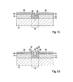
After structured lift-off layer 24 is formed, a conforming layer 28 made of a conductive material, including at least one metal, is formed. Conforming layer 28 completely covers the at least one position 16 of the at least one contact to be formed. In addition, conforming layer 28 at least partially covers first lift-off layer 24, as shown in FIG. 1C.
In particular, conforming layer 28 may be deposited over the entire surface, which may be easily carried out. Conforming layer 28 may be formed having a (preferably practically uniform) layer thickness d, which corresponds to a thickness of the at least one contact to be formed perpendicularly to surface 12 of substrate 10. (The layer of the contact is subsequently structured from the material which is deposited in the at least one position 16, i.e., which covers at least one surface 23 which is framed by inner wall surfaces 25.)
Conforming layer 28 made of the conductive material is preferably sputtered on. This ensures the desired conformity of conforming layer 28 for a contact which is formable from same. Conforming layer 28 may be made of nickel, a metal-nickel alloy, or an aluminum-cobalt alloy as the conductive material. Conforming layer 28 is preferably made of titanium-nickel. However, the designability of conforming layer 28 is not limited to the materials listed here.
During the application of conforming layer 28, lift-off layer 24 protects the areas covered by same from inadvertent direct contact with the material of conforming layer 28, in particular from inadvertent coating/covering by conforming layer 28. In addition, lift-off layer 24 ensures that the areas which it covers are reliably protected from diffusion of the at least one metal of conforming layer 28. In this way, insulation areas which are covered by lift-off layer 24 are also reliably protected from diffusion of the at least one metal of conforming layer 28, and thus, from contamination. In other words, lift-off layer 24 prevents the metal of conforming layer 28 from contacting areas outside the at least one position 16, i.e., the at least one desired contact area.
FIGS. 1D and 1E show cross sections of substrate 10 after at least one area 30 of conforming layer 28, which is situated in the at least one position 16/which covers at least one surface 23 framed by inner wall surfaces 25, has been covered by a mask 32. Mask 32 is formed with at least one continuous recess above a residual area 34 of conforming layer 28 situated externally from the at least one position. In particular, mask 32 may be formed in such a way that it has a clearance through residual area 34 as at least one continuous recess. In particular, the at least one continuous recess of mask 32 may subdivide the mask into separate subareas which are situated above the at least two positions 16/above the at least two surfaces 23. The subareas separated from each other preferably have a side edge 33 which is situated close to the edges of the associated position, i.e., close to inner wall surfaces 25. In other words, the structuring of mask 32 forms small “plaque-shaped” areas as mask 32. Mask 32 is preferably formed from a photoresist.
Mask 32 may be formed in such a way, for example, that the at least one side edge 33 is provided above the at least one inner wall surface 15 of insulating layer 14 (see FIG. 1D). To form this type of mask layout of mask 32, the same exposure mask may be used for structuring lift-off layer 24 and mask 32, lift-off layer 24 being formed from a “positive resist” and mask 32 being formed from a “negative resist.” When a “negative resist” is used, the method may also be referred to as a negative resist process. Instead of a negative resist process, the same exposure mask may be exposed, using modified exposure parameters, for structuring lift-off layer 24 and mask 32.
Alternatively, mask 32 may be designed in such a way that the at least one side edge 33 is provided above the at least one inner wall surface 25 of lift-off layer 24 or above surface 23 framed by the at least one inner wall surface 25 (see FIG. 1E). For this purpose, an exposure mask which is different from the one used for structuring lift-off layer 24 is used for structuring mask 32. This allows a more specific design of mask 32 with respect to the predefinable requirements, as is apparent from FIG. 1E.
FIG. 1F shows a cross section of substrate 10 after carrying out an etching process using mask 32. During the etching process, residual area 34 of conforming layer 28 which is not covered by mask 32 is at least partially etched away. After the etching process, preferably only area 30 of conforming layer 28 protected by mask 32 remains at least partially in or above the at least one position 16. It is thus possible to obtain attack surfaces for carrying out a lift-off process despite the conforming design of conforming layer 28. In particular, a solution used for the lift-off process is able to penetrate into the area between the remainder of conforming layer 28 and lift-off layer 24, and thus detach lift-off layer 24 from the material which it covers.
The etching process may be a wet or dry chemical etching process, for example. The etching solution used for the etching process is selective with respect to the conductive material of conforming layer 28. In contrast, mask 32 and the lift-off layer are slightly etched by the etching solution or not at all. However, the practicability of the etching process is not limited to a specific etching material.
Lift-off layer 24 also protects the areas underneath it during the etching of conforming layer 28. If partial residues of conforming layer 28 remain on the surface of the etched areas, these partial residues are situated on the lift-off layer. Thus, during the etching process there is no risk of metal residues of conforming layer 28 diffusing into an area to be protected. In particular oxide areas, such as a gate oxide area in or on substrate 10, are protected by lift-off layer 24 and therefore remain free of metal residues. The formation of metal silicide in polysilicon, which typically occurs during etching due to contamination by metal residues, is likewise prevented by lift-off layer 24.
A lift-off process is carried out after the etching process. In the lift-off process, lift-off layer 24 is removed, and the at least one layer 36 (as at least part of the contact) in the at least one position 16 is structured from the residue of conforming layer 28 which remains after the etching process. The result is shown in FIG. 1G.
Acetone may be used, for example, to tear off lift-off layer 24. However, the practicability of the lift-off process described here is not limited to the use of acetone. This method step may be reliably carried out due to the previously described advantageous formation of attack surfaces for a solution used in the lift-off process. In particular, in the lift-off process the solution is able to penetrate into the intermediate area, situated close to surface 23, between the remainder of conforming layer 28 and lift-off layer 24, which achieves good removability of lift-off layer 24 from the material which it covers.
The lift-off process may be carried out in such a way that tear-off marks are formed on at least one outer side area 40 between an outer base area 42 facing surface 12 and an outer contact area 44 facing away from surface 12 by tearing away material from (the remaining residue of) conforming layer 28. The tear-off marks result when lift-off layer 24 is removed by tearing away the material of conforming layer 28 adhering to same.
Mask 32 and lift-off layer 24 are also lifted during the lift-off process. Thus, only the at least one layer 36 remains in the at least one position 16. A layer 36 of a contact/a contact made of metal is produced for a defined contact area by forming the at least one layer 36 in the at least one position 16. An ohmic contact, for example, is achieved with the aid of formed layer 36. However, it is pointed out that the usability of layer 36 is not limited to use as an ohmic contact. In particular, the at least one layer 36 may be easily formed in an advantageous small size with the aid of the above-described method steps.
Insulating layer 14 remains free of metal residues, even after lift-off layer 24 which previously covered it has been removed. Thus, there is no concern that a metal remaining on the insulating layer may diffuse into substrate 10 in a further method step. The risk of diffusion of metal residues into the substrate is negligible, in particular also during a subsequent heat treatment step, for example a rapid thermal annealing (RTA) process for thermal activation. This type of heat treatment step may thus be easily carried out after the lift-off process. A cleaning process may also optionally be carried out after the lift-off process.
The at least one layer 36 situated on the surface of substrate 10 is preferably alloyed into a semiconductor material of substrate 10 with the aid of a heat treatment step. Examples of a suitable heat treatment step for this purpose are a rapid thermal annealing (RTA) process or a contact annealing step which may be carried out at a temperature above 1000° C., for example. Depending on the semiconductor material of substrate 10 and/or the conductive material of the at least one layer 36, a different temperature may also be set for carrying out the heat treatment step. The result of the heat treatment step is shown in FIG. 1H.
Layer 36 is preferably shaped and/or stabilized in the heat treatment step, which may also be referred to as a tempering process. Diffusion of metal outside the at least one position 16 is avoided due to the prevention of metal residues which has previously been carried out. Therefore, the heat treatment process is not limited with respect to temperature or time. The heat treatment process may typically have an overall process time of several minutes at temperatures around 1000° C. without concern for diffusion by metal.
It is pointed out once more that when the above-described method is carried out, semiconductor structures, for example a MOSFET design having a gate oxide situated on or in substrate 10, situated adjacent to the at least one position 16, are covered by lift-off layer 24 in particular during the application and etching of conforming layer 28. Thus, there is no concern that metal residues from conforming layer 28 will reach these structures. In particular, with the aid of the covering by lift-off layer 24, a gate oxide or a gate oxide covered with a polysilicon layer may also be protected in such a way that its continued reliability is ensured. In addition, metal residues, such as nickel residues in particular, may be prevented from diffusing into the structures and/or substrate 10 situated therebeneath. Furthermore, the formation of an undesirable metal silicide is prevented in this way.
FIGS. 2A and 2B show schematic illustrations of two specific embodiments of the semiconductor device.
The semiconductor devices schematically represented in FIGS. 2A and 2B include a substrate 10 and at least one contact, situated on or above a surface 12 of substrate 10, having at least one layer 36 made of a conductive material. The conductive material includes at least one metal. For example, layer 36 may be made of nickel, a metal-nickel alloy, or an aluminum-cobalt alloy as the conductive material. Layer 36 is preferably made of titanium-nickel. In one refinement, the contact may have at least one further layer in addition to layer 36 described here.
Layer 36 made of the conductive material is sputtered on at or above surface 12. The type of metal deposition may be deduced by an analysis of the metal structure of layer 36. In addition, layer 36 has tear-off marks on at least one outer side area 40 between an outer base area 42 facing surface 12 and an outer contact area 44 facing away from surface 12. It is thus apparent that layer 36 is structured from a sputtered-on, conforming layer via a lift-off process. While the at least one outer side area 40 has tear-off marks, the outer base area and/or outer contact area 44 is/are preferably free of tear-off marks.
The at least one contact/the at least one layer 36 may be formed using the above-described manufacturing method. However, the producibility of the at least one contact/the at least one layer 36 of the semiconductor devices in FIGS. 2A and 2B is not limited to strict adherence to the above-described method.
Layer 36 formed on surface 12 of substrate 10 is preferably alloyed into a semiconductor material of the substrate. The semiconductor material of substrate 10 may be silicon carbide, for example.
The semiconductor device schematically represented in FIG. 2A has a layer 36 which is offset in sections in a surface oriented parallel to surface 12. The design of layer 36 may also be described in such a way that layer 36 is composed of first subareas 50 which extend along a first axis 52, and second subareas 56 which extend along a second axis 54 which is parallel to first axis 52. A gap is present between two adjacent first subareas 50. Similarly, a gap is also provided between two adjacent second subareas 56. The distance between first axis 52 and second axis 54 corresponds to the sum of the lateral distances of the mutually facing sides of subareas 50 and 56 from axes 52 and 54, respectively. The respective gap widths are set to be smaller than the extensions of subareas 50 and 56 in such a way that in each case an end of a first subarea 50 facing an adjacent first subarea 50 (laterally) contacts a second subarea 56, while in each case an end of a second subarea 56 facing an adjacent second subarea 56 (laterally) contacts a first subarea 50.
However, the practicability of layer 36 is not limited to a design that is offset in sections. For example, the at least one layer 36 in the surface oriented parallel to surface 12 may also be meander-shaped or zigzag-shaped.
Due to the advantageous design of layer 36, this layer has a large number of edges or steps in relation to its volume. In addition, layer 36 has a comparatively large overall surface area of the at least one outer side area 40 in relation to its volume. Layer 36 thus provides good tear-off options which allow the lift-off process to be reliably carried out.
The semiconductor device schematically represented in FIG. 2B has multiple layers 36, each having a first extensional in a first spatial direction 20 oriented parallel to surface 12, which is identical to a second extension a2 along a second spatial direction 60, perpendicular to first spatial direction 20, oriented parallel to surface 12. This ensures the advantages listed in the description of FIG. 2A.
The lift-off process may be simplified with the aid of the above-described examples of an advantageous design modification. Compared to line structures, structures having a square surface area, those that are meander-shaped, zigzag-shaped, or are offset in sections have improved suppression of metal residues at edges of the lift-off layer. Metal residues are not expected to be a problem for the two described design modifications.

Claims (10)

What is claimed is:
1. A method for manufacturing a semiconductor device having at least one contact, the method comprising:
forming a lift-off layer on an insulating layer at least partially covering a surface of a substrate, a continuous recess in the lift-off layer and the insulating layer being provided at at least one position of at least one contact to be formed, the insulating layer having inner walls covered by the lift-off layer;
forming a conforming layer made of a conductive material including at least one metal, which completely covers the at least one position of the at least one contact to be formed and a portion of the lift-off layer covering the inner walls of the insulating layer;
covering at least one area of the conforming layer, situated in the at least one position, with a mask which is formed with at least one continuous recess above a residual area of the conforming layer situated externally from the at least one position;
carrying out an etching process, the residual area being at least partially etched away during the etching process; and
carrying out a lift-off process, the lift-off layer being removed and at least one layer being structured out as at least part of the at least one contact in the at least one position, wherein tear-off marks are formed on at least one outer side area between an outer base area facing the surface and an outer contact area facing away from the surface during removal of the lift-off layer by tearing away the residual area remaining after the etching process;
wherein the method includes only one negative resist step.
2. The method as recited in claim 1, wherein the conforming layer made of the conductive material is sputtered on.
3. The method as recited in claim 1, wherein at least one of the lift-off layer and the mask are formed from a photoresist.
4. The method as recited in claim 1, wherein the at least one layer is formed on the surface of the substrate and is alloyed into a semiconductor material of the substrate with the aid of a heat treatment step.
5. The method as recited in claim 1, wherein the conforming layer is made of one of nickel, a metal-nickel alloy, or an aluminum-cobalt alloy, as the conductive material.
6. The method as recited in claim 1, wherein the at least one continuous recess in the lift-off layer is formed having a first extension in a first spatial direction oriented parallel to the surface, which is identical to a second extension along a second spatial direction, perpendicular to the first spatial direction, oriented parallel to the surface.
7. The method as recited in claim 1, wherein the at least one continuous recess in the lift-off layer has a framing surface which is at least one of meander-shaped, zigzag-shaped, and offset, in sections.
8. The method of claim 1, wherein the at least one area of the conforming layer is covered such that the mask does not directly contact least one of: the surface of the substrate, the lift-off layer, and the insulating layer in the cross-sectional view.
9. The method of claim 1, wherein the conforming layer is a continuous layer.
10. The method of claim 1, wherein the inner walls of the insulating layer directly contact the lift-off layer.
US13/446,531 2011-05-16 2012-04-13 Semiconductor device having at least one contact, and manufacturing method for a semiconductor device having at least one contact Expired - Fee Related US9202702B2 (en)

Applications Claiming Priority (3)

Application Number Priority Date Filing Date Title
DE102011075888 2011-05-16
DE201110075888 DE102011075888B4 (en) 2011-05-16 2011-05-16 Semiconductor device with at least one contact and method for producing a semiconductor device with at least one contact
DE102011075888.7 2011-05-16

Publications (2)

Publication Number Publication Date
US20120292641A1 US20120292641A1 (en) 2012-11-22
US9202702B2 true US9202702B2 (en) 2015-12-01

Family

ID=47087891

Family Applications (1)

Application Number Title Priority Date Filing Date
US13/446,531 Expired - Fee Related US9202702B2 (en) 2011-05-16 2012-04-13 Semiconductor device having at least one contact, and manufacturing method for a semiconductor device having at least one contact

Country Status (2)

Country Link
US (1) US9202702B2 (en)
DE (1) DE102011075888B4 (en)

Families Citing this family (1)

* Cited by examiner, † Cited by third party
Publication number Priority date Publication date Assignee Title
DE102014205839B3 (en) * 2014-03-28 2015-05-07 Robert Bosch Gmbh Method of making a bond pad and device made therefrom

Citations (10)

* Cited by examiner, † Cited by third party
Publication number Priority date Publication date Assignee Title
JPS5984550A (en) 1982-11-08 1984-05-16 Hitachi Ltd Manufacture of semiconductor device
US5091288A (en) * 1989-10-27 1992-02-25 Rockwell International Corporation Method of forming detector array contact bumps for improved lift off of excess metal
US5176792A (en) 1991-10-28 1993-01-05 At&T Bell Laboratories Method for forming patterned tungsten layers
US5270252A (en) 1988-10-25 1993-12-14 United States Of America As Represented By The Secretary Of The Navy Method of forming platinum and platinum silicide schottky contacts on beta-silicon carbide
US5360697A (en) * 1992-02-27 1994-11-01 Eastman Kodak Company Forming self-aligned diffusion barriers in solid state devices using lift-off process
US5397741A (en) * 1993-03-29 1995-03-14 International Business Machines Corporation Process for metallized vias in polyimide
US5705432A (en) 1995-12-01 1998-01-06 Hughes Aircraft Company Process for providing clean lift-off of sputtered thin film layers
JP2000058481A (en) 1998-08-05 2000-02-25 Sanyo Electric Co Ltd Formation of electrode for compound semiconductor
US20030153178A1 (en) * 2002-02-05 2003-08-14 Maile Bernd E. Method of fabricating a vertically profiled electrode and semiconductor device comprising such an electrode
US20060292868A1 (en) * 2002-12-16 2006-12-28 Fuji Xerox Co., Ltd. Surface emitting semiconductor laser

Patent Citations (11)

* Cited by examiner, † Cited by third party
Publication number Priority date Publication date Assignee Title
JPS5984550A (en) 1982-11-08 1984-05-16 Hitachi Ltd Manufacture of semiconductor device
US5270252A (en) 1988-10-25 1993-12-14 United States Of America As Represented By The Secretary Of The Navy Method of forming platinum and platinum silicide schottky contacts on beta-silicon carbide
US5091288A (en) * 1989-10-27 1992-02-25 Rockwell International Corporation Method of forming detector array contact bumps for improved lift off of excess metal
US5176792A (en) 1991-10-28 1993-01-05 At&T Bell Laboratories Method for forming patterned tungsten layers
DE69228044T2 (en) 1991-10-28 1999-08-19 At & T Corp Process for structuring tungsten layers
US5360697A (en) * 1992-02-27 1994-11-01 Eastman Kodak Company Forming self-aligned diffusion barriers in solid state devices using lift-off process
US5397741A (en) * 1993-03-29 1995-03-14 International Business Machines Corporation Process for metallized vias in polyimide
US5705432A (en) 1995-12-01 1998-01-06 Hughes Aircraft Company Process for providing clean lift-off of sputtered thin film layers
JP2000058481A (en) 1998-08-05 2000-02-25 Sanyo Electric Co Ltd Formation of electrode for compound semiconductor
US20030153178A1 (en) * 2002-02-05 2003-08-14 Maile Bernd E. Method of fabricating a vertically profiled electrode and semiconductor device comprising such an electrode
US20060292868A1 (en) * 2002-12-16 2006-12-28 Fuji Xerox Co., Ltd. Surface emitting semiconductor laser

Non-Patent Citations (2)

* Cited by examiner, † Cited by third party
Title
IBM, "Electrical Measurement of Sputter Deposition Rate of Trenches," IBM Technical Disclosure Bulletin, vol. 35, No. 5, pp. 490-492, 1992.
Rossnagel, S. et al., "Collimated Magnetron Sputter Disposition," Journal of Vacuum Science and Technology, vol. 35, No. 2, pp. 261-265, 1991.

Also Published As

Publication number Publication date
DE102011075888B4 (en) 2014-07-10
US20120292641A1 (en) 2012-11-22
DE102011075888A1 (en) 2012-11-22

Similar Documents

Publication Publication Date Title
JP5105824B2 (en) Method for forming mask structure and method for forming fine pattern using the same
CN109319726B (en) Piezoelectric microphone with deflection control and method of manufacturing the same
JP2008119817A (en) Mems device and its manufacturing method
KR940020531A (en) Manufacturing method of metal plug in contact hole
US9202702B2 (en) Semiconductor device having at least one contact, and manufacturing method for a semiconductor device having at least one contact
KR102646859B1 (en) Platinum patterning by alloying and etching platinum alloys
US8338914B2 (en) Integrated process for thin film resistors with silicides
US20060110842A1 (en) Method and apparatus for preventing metal/silicon spiking in MEMS devices
JP2006332180A (en) Manufacturing method of silicon carbide semiconductor device
US6331460B1 (en) Method of fabricating a mom capacitor having a metal silicide barrier
US11027969B2 (en) Micro-device having a metal-semiconductor compound layer protected against HF etching and method for making the same
JP2004509465A (en) Isotropic resistive protective etching to aid residue removal
US8569171B2 (en) Mask-based silicidation for FEOL defectivity reduction and yield boost
TWI802629B (en) A method for producing a micromechanical layer structure, and a micromechanical layer structure
US10777522B2 (en) Semiconductor structure and method of manufacturing the same
JP2005038981A (en) Manufacturing method of thin film transistor panel
JP2000114464A (en) Manufacture of thin-film resistor
US9978686B1 (en) Interconnection of semiconductor devices in extreme environment microelectronic integrated circuit chips
JP3023298B2 (en) Semiconductor device and manufacturing method thereof
TWI253533B (en) Manufacturing method of gate, thin film transistor, and pixel
JP2009289891A (en) Manufacturing method of semiconductor device
US20080048346A1 (en) Method of fabricating conductive lines and structure of the same
US8853797B2 (en) MEMS devices and fabrication thereof
US8536014B2 (en) Self aligned silicide device fabrication
CN114577371A (en) Capacitive pressure sensor and method for manufacturing the same

Legal Events

Date Code Title Description
AS Assignment

Owner name: ROBERT BOSCH GMBH, GERMANY

Free format text: ASSIGNMENT OF ASSIGNORS INTEREST;ASSIGNORS:SCHREY, FREDERIK;TRAUTMANN, ACHIM;RUDHARD, JOACHIM;SIGNING DATES FROM 20120430 TO 20120507;REEL/FRAME:028441/0091

STCF Information on status: patent grant

Free format text: PATENTED CASE

MAFP Maintenance fee payment

Free format text: PAYMENT OF MAINTENANCE FEE, 4TH YEAR, LARGE ENTITY (ORIGINAL EVENT CODE: M1551); ENTITY STATUS OF PATENT OWNER: LARGE ENTITY

Year of fee payment: 4

FEPP Fee payment procedure

Free format text: MAINTENANCE FEE REMINDER MAILED (ORIGINAL EVENT CODE: REM.); ENTITY STATUS OF PATENT OWNER: LARGE ENTITY

LAPS Lapse for failure to pay maintenance fees

Free format text: PATENT EXPIRED FOR FAILURE TO PAY MAINTENANCE FEES (ORIGINAL EVENT CODE: EXP.); ENTITY STATUS OF PATENT OWNER: LARGE ENTITY

STCH Information on status: patent discontinuation

Free format text: PATENT EXPIRED DUE TO NONPAYMENT OF MAINTENANCE FEES UNDER 37 CFR 1.362

FP Lapsed due to failure to pay maintenance fee

Effective date: 20231201