US9230886B2 - Method for forming through silicon via with wafer backside protection - Google Patents

Method for forming through silicon via with wafer backside protection Download PDF

Info

Publication number
US9230886B2
US9230886B2 US14/575,639 US201414575639A US9230886B2 US 9230886 B2 US9230886 B2 US 9230886B2 US 201414575639 A US201414575639 A US 201414575639A US 9230886 B2 US9230886 B2 US 9230886B2
Authority
US
United States
Prior art keywords
silicon
tsv
layer
composite layer
silicon substrate
Prior art date
Legal status (The legal status is an assumption and is not a legal conclusion. Google has not performed a legal analysis and makes no representation as to the accuracy of the status listed.)
Active
Application number
US14/575,639
Other versions
US20150137359A1 (en
Inventor
Lup San Leong
Zheng Zou
Alex Kai Hung See
Hai Cong
Xuesong Rao
Yun Ling Tan
Huang Liu
Current Assignee (The listed assignees may be inaccurate. Google has not performed a legal analysis and makes no representation or warranty as to the accuracy of the list.)
GlobalFoundries Singapore Pte Ltd
Original Assignee
GlobalFoundries Singapore Pte Ltd
Priority date (The priority date is an assumption and is not a legal conclusion. Google has not performed a legal analysis and makes no representation as to the accuracy of the date listed.)
Filing date
Publication date
Application filed by GlobalFoundries Singapore Pte Ltd filed Critical GlobalFoundries Singapore Pte Ltd
Priority to US14/575,639 priority Critical patent/US9230886B2/en
Publication of US20150137359A1 publication Critical patent/US20150137359A1/en
Assigned to GLOBALFOUNDRIES Singapore Pte.Ltd. reassignment GLOBALFOUNDRIES Singapore Pte.Ltd. ASSIGNMENT OF ASSIGNORS INTEREST (SEE DOCUMENT FOR DETAILS). Assignors: HUNG SEE, ALEX KAI, CONG, Hai, LEONG, LUP SAN, LIU, Huang, RAO, XUESONG, TAN, YUN LING, ZOU, Zheng
Application granted granted Critical
Publication of US9230886B2 publication Critical patent/US9230886B2/en
Assigned to WILMINGTON TRUST, NATIONAL ASSOCIATION reassignment WILMINGTON TRUST, NATIONAL ASSOCIATION SECURITY AGREEMENT Assignors: GLOBALFOUNDRIES INC.
Assigned to GLOBALFOUNDRIES INC. reassignment GLOBALFOUNDRIES INC. RELEASE BY SECURED PARTY (SEE DOCUMENT FOR DETAILS). Assignors: WILMINGTON TRUST, NATIONAL ASSOCIATION
Active legal-status Critical Current
Anticipated expiration legal-status Critical

Links

Images

Classifications

    • HELECTRICITY
    • H01ELECTRIC ELEMENTS
    • H01LSEMICONDUCTOR DEVICES NOT COVERED BY CLASS H10
    • H01L23/00Details of semiconductor or other solid state devices
    • H01L23/48Arrangements for conducting electric current to or from the solid state body in operation, e.g. leads, terminal arrangements ; Selection of materials therefor
    • H01L23/481Internal lead connections, e.g. via connections, feedthrough structures
    • HELECTRICITY
    • H01ELECTRIC ELEMENTS
    • H01LSEMICONDUCTOR DEVICES NOT COVERED BY CLASS H10
    • H01L21/00Processes or apparatus adapted for the manufacture or treatment of semiconductor or solid state devices or of parts thereof
    • H01L21/70Manufacture or treatment of devices consisting of a plurality of solid state components formed in or on a common substrate or of parts thereof; Manufacture of integrated circuit devices or of parts thereof
    • H01L21/71Manufacture of specific parts of devices defined in group H01L21/70
    • H01L21/768Applying interconnections to be used for carrying current between separate components within a device comprising conductors and dielectrics
    • H01L21/76898Applying interconnections to be used for carrying current between separate components within a device comprising conductors and dielectrics formed through a semiconductor substrate
    • HELECTRICITY
    • H01ELECTRIC ELEMENTS
    • H01LSEMICONDUCTOR DEVICES NOT COVERED BY CLASS H10
    • H01L21/00Processes or apparatus adapted for the manufacture or treatment of semiconductor or solid state devices or of parts thereof
    • H01L21/02Manufacture or treatment of semiconductor devices or of parts thereof
    • H01L21/02104Forming layers
    • H01L21/02107Forming insulating materials on a substrate
    • HELECTRICITY
    • H01ELECTRIC ELEMENTS
    • H01LSEMICONDUCTOR DEVICES NOT COVERED BY CLASS H10
    • H01L21/00Processes or apparatus adapted for the manufacture or treatment of semiconductor or solid state devices or of parts thereof
    • H01L21/02Manufacture or treatment of semiconductor devices or of parts thereof
    • H01L21/04Manufacture or treatment of semiconductor devices or of parts thereof the devices having at least one potential-jump barrier or surface barrier, e.g. PN junction, depletion layer or carrier concentration layer
    • H01L21/48Manufacture or treatment of parts, e.g. containers, prior to assembly of the devices, using processes not provided for in a single one of the subgroups H01L21/06 - H01L21/326
    • H01L21/4814Conductive parts
    • H01L21/4846Leads on or in insulating or insulated substrates, e.g. metallisation
    • H01L21/486Via connections through the substrate with or without pins
    • HELECTRICITY
    • H01ELECTRIC ELEMENTS
    • H01LSEMICONDUCTOR DEVICES NOT COVERED BY CLASS H10
    • H01L24/00Arrangements for connecting or disconnecting semiconductor or solid-state bodies; Methods or apparatus related thereto
    • H01L24/01Means for bonding being attached to, or being formed on, the surface to be connected, e.g. chip-to-package, die-attach, "first-level" interconnects; Manufacturing methods related thereto
    • H01L24/10Bump connectors ; Manufacturing methods related thereto
    • H01L24/12Structure, shape, material or disposition of the bump connectors prior to the connecting process
    • H01L24/13Structure, shape, material or disposition of the bump connectors prior to the connecting process of an individual bump connector
    • HELECTRICITY
    • H01ELECTRIC ELEMENTS
    • H01LSEMICONDUCTOR DEVICES NOT COVERED BY CLASS H10
    • H01L24/00Arrangements for connecting or disconnecting semiconductor or solid-state bodies; Methods or apparatus related thereto
    • H01L24/01Means for bonding being attached to, or being formed on, the surface to be connected, e.g. chip-to-package, die-attach, "first-level" interconnects; Manufacturing methods related thereto
    • H01L24/10Bump connectors ; Manufacturing methods related thereto
    • H01L24/15Structure, shape, material or disposition of the bump connectors after the connecting process
    • H01L24/16Structure, shape, material or disposition of the bump connectors after the connecting process of an individual bump connector
    • HELECTRICITY
    • H01ELECTRIC ELEMENTS
    • H01LSEMICONDUCTOR DEVICES NOT COVERED BY CLASS H10
    • H01L2224/00Indexing scheme for arrangements for connecting or disconnecting semiconductor or solid-state bodies and methods related thereto as covered by H01L24/00
    • H01L2224/01Means for bonding being attached to, or being formed on, the surface to be connected, e.g. chip-to-package, die-attach, "first-level" interconnects; Manufacturing methods related thereto
    • H01L2224/10Bump connectors; Manufacturing methods related thereto
    • H01L2224/12Structure, shape, material or disposition of the bump connectors prior to the connecting process
    • H01L2224/13Structure, shape, material or disposition of the bump connectors prior to the connecting process of an individual bump connector
    • H01L2224/13001Core members of the bump connector
    • H01L2224/13005Structure
    • H01L2224/13009Bump connector integrally formed with a via connection of the semiconductor or solid-state body
    • HELECTRICITY
    • H01ELECTRIC ELEMENTS
    • H01LSEMICONDUCTOR DEVICES NOT COVERED BY CLASS H10
    • H01L2224/00Indexing scheme for arrangements for connecting or disconnecting semiconductor or solid-state bodies and methods related thereto as covered by H01L24/00
    • H01L2224/01Means for bonding being attached to, or being formed on, the surface to be connected, e.g. chip-to-package, die-attach, "first-level" interconnects; Manufacturing methods related thereto
    • H01L2224/10Bump connectors; Manufacturing methods related thereto
    • H01L2224/12Structure, shape, material or disposition of the bump connectors prior to the connecting process
    • H01L2224/13Structure, shape, material or disposition of the bump connectors prior to the connecting process of an individual bump connector
    • H01L2224/1354Coating
    • H01L2224/1357Single coating layer

Definitions

  • the present disclosure relates to a method of fabricating semiconductor devices with through silicon vias (TSVs).
  • TSVs through silicon vias
  • the present disclosure is particularly applicable to fabricating semiconductor devices with TSVs with wafer backside protection from copper contamination.
  • An aspect of the present disclosure is an efficient method of fabricating a semiconductor device with wafer backside protection from copper contamination.
  • Another aspect of the present disclosure is a semiconductor device including a wafer backside protection layer surrounding an exposed TSV.
  • some technical effects may be achieved in part by a method including: exposing a passivation layer surrounding a bottom portion of a TSV in a silicon substrate, forming a silicon composite layer over the exposed passivation layer and over a bottom surface of the silicon substrate, forming a hardmask layer over the silicon composite layer and over the bottom surface of the silicon substrate, removing a section of the silicon composite layer around the bottom portion of the TSV using the hardmask layer as a mask, re-exposing the passivation layer, and removing the hardmask layer and the re-exposed passivation layer to expose a contact for the bottom portion of the TSV.
  • aspects of the present disclosure include forming the hardmask layer of a spin-on resist or planarization film.
  • An additional aspect includes removing the section of the silicon composite layer by wet etching, dry etching, or a combination thereof.
  • Another aspect includes removing the hardmask layer and the passivation layer by wet etching, dry etching, or a combination thereof.
  • Further aspects include forming an oxide layer over the bottom portion of the TSV and the bottom surface of the silicon substrate prior to forming the silicon composite layer, and removing the oxide layer over the bottom portion of the TSV concurrently with the hardmask layer and the passivation layer to expose a contact for the bottom portion of the TSV.
  • Yet another aspect includes forming a mask with the hardmask layer by forming the hardmask layer over the entire silicon composite layer and planarizing down to the silicon composite layer over the bottom portion of the TSV to expose the section of the silicon composite layer.
  • An additional aspect includes planarizing the hardmask layer by chemical mechanical polishing, wet etching, or a combination thereof, exposing the section of the silicon composite layer.
  • Other aspects including removing a protective film under the passivation layer from a bottom surface of the TSV after removing the hardmask layer and the passivation layer to expose the contact for the bottom portion of the TSV.
  • a further aspect includes forming the hardmask layer to a thickness of 1 ⁇ m to 3 ⁇ m.
  • Another aspect of the present disclosure includes backgrinding a bottom surface of a silicon substrate exposing a bottom portion of a TSV surrounded by a passivation layer and a protective layer, forming an oxide layer over the bottom portion of the TSV, forming a silicon composite layer over the bottom portion of the TSV and the bottom surface of the silicon substrate, forming a hardmask layer over the silicon composite layer, planarizing the hardmask layer down to the silicon composite layer over a bottom surface of the TSV, and removing a section of the silicon composite layer around the bottom portion of the TSV.
  • An additional aspect includes removing the passivation layer and the protective layer to expose a contact for the bottom surface of the TSV.
  • Yet another aspect includes planarizing the hardmask layer by chemical mechanical polishing, wet etching, or a combination thereof to expose the section of the silicon composite layer.
  • Another aspect of the present disclosure is a device including: a silicon substrate, an exposed portion of a through silicon via (TSV) protruding out from a bottom surface of the silicon substrate, and a silicon composite layer covering the remaining bottom surface of the silicon substrate.
  • TSV through silicon via
  • aspects include a device including an oxide layer between the silicon substrate and the silicon composite layer.
  • An additional aspect includes the oxide layer being formed to a thickness of 100 ⁇ to 500 ⁇ .
  • a further aspect includes the silicon composite layer being formed of silicon nitride, silicon carbide, or a combination thereof.
  • Another aspect includes the exposed portion of the TSV protruding 0.5 ⁇ m to 3 ⁇ m out from the bottom surface of the silicon substrate.
  • An additional aspect includes the device including a protective film and a passivation layer between the TSV and the silicon substrate.
  • a further aspect includes the passivation layer ending at the bottom surface of the silicon composite layer.
  • Yet another aspect includes the protective layer extending down sides of the exposed portion of the TSV.
  • FIGS. 1 through 9 schematically illustrate wafer backside protection steps and a resulting substrate including a TSV and a backside contamination protection layer, in accordance with an exemplary embodiment.
  • the present disclosure addresses and solves the current problem of semiconductor device failure because of copper contamination during backgrinding owing to no gettering layer at the back surface of thinned wafer semiconductors and from copper TSVs owing to poor step coverage of the barrier layer.
  • a backside wafer contamination protection layer is produced prior to exposing the bottom of the TSV.
  • Methodology in accordance with embodiments of the present disclosure includes exposing a passivation layer surrounding a bottom portion of a TSV in a silicon substrate.
  • a silicon composite layer is then formed over the exposed passivation layer and over a bottom surface of the silicon substrate.
  • a hardmask layer of a spin-on resist or planarization film is formed over the silicon composite layer and over the bottom surface of the silicon substrate.
  • a mask made using the hardmask layer may be formed by forming the hardmask layer over the entire silicon composite layer and planarizing down to the silicon composite layer over a bottom portion of the TSV to expose a section of the silicon composite layer.
  • the section of the silicon composite layer around the bottom portion of the TSV is removed by wet etching, dry etching, or a combination thereof using the mask of the hardmask layer, re-exposing the passivation layer. Then, the hardmask layer and the re-exposed passivation layer are removed exposing a contact for the bottom portion of the TSV.
  • a method of forming a semiconductor device with wafer backside protection from copper contamination begins with a silicon substrate 100 including a TSV 101 surrounded by a protective film 103 and a passivation layer 105 .
  • the protective film 103 is contiguous with the TSV 101 and the passivation layer 105
  • the passivation layer is contiguous with the silicon substrate 100 .
  • the TSV 101 may be made of any conductive metal, such as copper (Cu).
  • the protective film 103 may be formed of tantalum (Ta) or tantalum nitride (TaN).
  • the passivation layer 105 may be formed of tetraethyl orthosilicate (TEOS) or any other passivation material.
  • the method proceeds with backgrinding of the silicon substrate 100 down to approximately the passivation layer 105 , followed by etching of the silicon substrate 100 to expose a bottom portion 201 of the TSV 101 .
  • the etching of the silicon substrate 100 may be accomplished using ammonium hydroxide (NH 4 OH), potassium hydroxide (KOH), or a combination thereof.
  • the bottom portion 201 of the TSV 101 may protrude 0.5 to 3 ⁇ m (e.g., 1 ⁇ m) from the bottom surface of the silicon substrate 100 .
  • an oxide layer 301 is formed over the bottom portion 201 of the TSV 101 and the bottom surface of the silicon substrate 100 , as illustrated in FIG. 3 .
  • the oxide layer 301 may be formed of TEOS, a high aspect ratio oxide (HARP), amorphous hydrogenated carbon doped silicon oxide (SiCOH) and other doped silicon oxides.
  • the oxide layer 301 may be formed to a thickness of 100 to 500 ⁇ (e.g., 300 ⁇ ).
  • a silicon composite layer 401 is formed over the oxide layer 301 .
  • the silicon composite layer 401 may be formed of silicon nitride (SiN), silicon carbide (SiC), or a combination thereof at a thickness of 500 to 1000 ⁇ (e.g., 750 ⁇ ).
  • the silicon composite layer 401 may act as a backside contamination protection layer during the exposure of the TSV.
  • FIGS. 5A and 5B illustrate various embodiments for forming a hardmask layer 501 over the silicon composite layer 401 .
  • the hardmask layer 501 may be formed to a thickness of 1 to 3 ⁇ m (e.g., 1 ⁇ m) and may be formed of TEOS.
  • the hardmask layer 501 may be deposited over the silicon composite layer 401 .
  • the hardmask layer 501 may be deposited according to any known deposition method, such as chemical vapor deposition.
  • a mask is created using the hardmask layer 501 by removing the hardmask layer 501 down to the silicon composite layer 401 over the bottom portion of the TSV 101 , to expose a section 601 of the silicon composite layer 401 .
  • the hardmask layer 501 may then be planarized using a fixed abrasive, low selectivity chemical mechanical polish (CMP) slurry, such as CMP platen 2 to expose the section 601 of the silicon composite layer 401 .
  • CMP chemical mechanical polish
  • the hardmask layer 501 may instead be formed of a spin-on resist or a planarization film followed by a hard bake at 100 to 550° C. Subsequently, the mask of FIG. 6 may be created by removing the hardmask layer 501 down to the silicon composite layer 401 over the bottom portion 201 of the TSV 101 to expose the section 601 of the silicon composite layer 401 using a wet etch that removes TEOS. Alternatively, a combination of planarization and wet etching may be used.
  • the section 601 of the silicon composite layer 401 may be removed by wet etching, dry etching, or a combination thereof.
  • the section 601 of the silicon composite layer 401 may be removed by a wet etch using phosphoric acid (H 3 PO 4 ).
  • the remaining hardmask layer 501 , the exposed portion of the oxide layer 301 , and a portion the passivation layer 105 may be removed by wet etching, dry etching, or a combination thereof to re-expose the bottom portion 201 of the TSV 101 .
  • the bottom portion 201 is exposed in FIG. 8 without the passivation layer 105 .
  • the remaining hardmask layer 501 , the exposed portion of the oxide layer 301 , and a portion the passivation layer 105 may be removed by a wet etch with dilute hydrofluoric acid (HF).
  • the re-exposed bottom portion 201 of the TSV 101 may still include the protective film 103 .
  • the protective film 103 may be removed from the bottom surface of the re-exposed bottom portion 201 by CMP or other methods (e.g., RIE), to expose a contact 901 for the bottom portion 201 of the TSV 101 .
  • Embodiments of the present disclosure achieve several technical effects, including preventing copper contamination at the backside of wafers during TSV exposure.
  • Embodiments of the present disclosure enjoy utility in various industrial applications as, for example, microprocessors, smart phones, mobile phones, cellular handsets, set-top boxes, DVD recorders and players, automotive navigation, printers and peripherals, networking and telecom equipment, gaming systems, and digital cameras.
  • the present disclosure therefore enjoys industrial applicability in any of various types of highly integrated semiconductor devices.

Abstract

Semiconductor devices with through silicon vias (TSVs) are formed without copper contamination. Embodiments include exposing a passivation layer surrounding a bottom portion of a TSV in a silicon substrate, forming a silicon composite layer over the exposed passivation layer and over a bottom surface of the silicon substrate, forming a hardmask layer over the silicon composite layer and over the bottom surface of the silicon substrate, removing a section of the silicon composite layer around the bottom portion of the TSV using the hardmask layer as a mask, re-exposing the passivation layer, and removing the hardmask layer and the re-exposed passivation layer to expose a contact for the bottom portion of the TSV.

Description

CROSS REFERENCE TO RELATED APPLICATION
This Application is a Divisional of U.S. application Ser. No. 13/542,256, filed Jul. 5, 2012, the content of which is incorporated herein by reference in its entirety.
TECHNICAL FIELD
The present disclosure relates to a method of fabricating semiconductor devices with through silicon vias (TSVs). The present disclosure is particularly applicable to fabricating semiconductor devices with TSVs with wafer backside protection from copper contamination.
BACKGROUND
The integration of hundreds of millions of circuit elements, such as transistors, on a single integrated circuit necessitates further scaling down or micro-miniaturization of the physical dimensions of the circuit elements, including interconnection structures. Micro-miniaturization has engendered a dramatic increase in transistor engineering complexity, resulting in several problems.
One such problem is copper contamination at the backside surface of silicon wafers during TSV exposure by backgrind and reactive ion etch (RIE). The TSV exposure and RIE can cause copper ion migration into active device regions. This issue is especially problematic after wafer thinning.
A need therefore exists for methodology enabling formation of devices including TSVs with wafer backside protection from copper contamination, and the resulting device.
SUMMARY
An aspect of the present disclosure is an efficient method of fabricating a semiconductor device with wafer backside protection from copper contamination.
Another aspect of the present disclosure is a semiconductor device including a wafer backside protection layer surrounding an exposed TSV.
Additional aspects and other features of the present disclosure will be set forth in the description which follows and in part will be apparent to those having ordinary skill in the art upon examination of the following or may be learned from the practice of the present disclosure. The advantages of the present disclosure may be realized and obtained as particularly pointed out in the appended claims.
According to the present disclosure, some technical effects may be achieved in part by a method including: exposing a passivation layer surrounding a bottom portion of a TSV in a silicon substrate, forming a silicon composite layer over the exposed passivation layer and over a bottom surface of the silicon substrate, forming a hardmask layer over the silicon composite layer and over the bottom surface of the silicon substrate, removing a section of the silicon composite layer around the bottom portion of the TSV using the hardmask layer as a mask, re-exposing the passivation layer, and removing the hardmask layer and the re-exposed passivation layer to expose a contact for the bottom portion of the TSV.
Aspects of the present disclosure include forming the hardmask layer of a spin-on resist or planarization film. An additional aspect includes removing the section of the silicon composite layer by wet etching, dry etching, or a combination thereof. Another aspect includes removing the hardmask layer and the passivation layer by wet etching, dry etching, or a combination thereof. Further aspects include forming an oxide layer over the bottom portion of the TSV and the bottom surface of the silicon substrate prior to forming the silicon composite layer, and removing the oxide layer over the bottom portion of the TSV concurrently with the hardmask layer and the passivation layer to expose a contact for the bottom portion of the TSV. Yet another aspect includes forming a mask with the hardmask layer by forming the hardmask layer over the entire silicon composite layer and planarizing down to the silicon composite layer over the bottom portion of the TSV to expose the section of the silicon composite layer. An additional aspect includes planarizing the hardmask layer by chemical mechanical polishing, wet etching, or a combination thereof, exposing the section of the silicon composite layer. Other aspects including removing a protective film under the passivation layer from a bottom surface of the TSV after removing the hardmask layer and the passivation layer to expose the contact for the bottom portion of the TSV. A further aspect includes forming the hardmask layer to a thickness of 1 μm to 3 μm.
Another aspect of the present disclosure includes backgrinding a bottom surface of a silicon substrate exposing a bottom portion of a TSV surrounded by a passivation layer and a protective layer, forming an oxide layer over the bottom portion of the TSV, forming a silicon composite layer over the bottom portion of the TSV and the bottom surface of the silicon substrate, forming a hardmask layer over the silicon composite layer, planarizing the hardmask layer down to the silicon composite layer over a bottom surface of the TSV, and removing a section of the silicon composite layer around the bottom portion of the TSV.
An additional aspect includes removing the passivation layer and the protective layer to expose a contact for the bottom surface of the TSV. Yet another aspect includes planarizing the hardmask layer by chemical mechanical polishing, wet etching, or a combination thereof to expose the section of the silicon composite layer.
Another aspect of the present disclosure is a device including: a silicon substrate, an exposed portion of a through silicon via (TSV) protruding out from a bottom surface of the silicon substrate, and a silicon composite layer covering the remaining bottom surface of the silicon substrate.
Aspects include a device including an oxide layer between the silicon substrate and the silicon composite layer. An additional aspect includes the oxide layer being formed to a thickness of 100 Å to 500 Å. A further aspect includes the silicon composite layer being formed of silicon nitride, silicon carbide, or a combination thereof. Another aspect includes the exposed portion of the TSV protruding 0.5 μm to 3 μm out from the bottom surface of the silicon substrate. An additional aspect includes the device including a protective film and a passivation layer between the TSV and the silicon substrate. A further aspect includes the passivation layer ending at the bottom surface of the silicon composite layer. Yet another aspect includes the protective layer extending down sides of the exposed portion of the TSV.
Additional aspects and technical effects of the present disclosure will become readily apparent to those skilled in the art from the following detailed description wherein embodiments of the present disclosure are described simply by way of illustration of the best mode contemplated to carry out the present disclosure. As will be realized, the present disclosure is capable of other and different embodiments, and its several details are capable of modifications in various obvious respects, all without departing from the present disclosure. Accordingly, the drawings and description are to be regarded as illustrative in nature, and not as restrictive.
BRIEF DESCRIPTION OF THE DRAWINGS
The present disclosure is illustrated by way of example, and not by way of limitation, in the figures of the accompanying drawings and in which like reference numerals refer to similar elements and in which:
FIGS. 1 through 9 schematically illustrate wafer backside protection steps and a resulting substrate including a TSV and a backside contamination protection layer, in accordance with an exemplary embodiment.
DETAILED DESCRIPTION
In the following description, for the purposes of explanation, numerous specific details are set forth in order to provide a thorough understanding of exemplary embodiments. It should be apparent, however, that exemplary embodiments may be practiced without these specific details or with an equivalent arrangement. In other instances, well-known structures and devices are shown in block diagram form in order to avoid unnecessarily obscuring exemplary embodiments. In addition, unless otherwise indicated, all numbers expressing quantities, ratios, and numerical properties of ingredients, reaction conditions, and so forth used in the specification and claims are to be understood as being modified in all instances by the term “about.”
The present disclosure addresses and solves the current problem of semiconductor device failure because of copper contamination during backgrinding owing to no gettering layer at the back surface of thinned wafer semiconductors and from copper TSVs owing to poor step coverage of the barrier layer. In accordance with embodiments of the present disclosure, a backside wafer contamination protection layer is produced prior to exposing the bottom of the TSV.
Methodology in accordance with embodiments of the present disclosure includes exposing a passivation layer surrounding a bottom portion of a TSV in a silicon substrate. A silicon composite layer is then formed over the exposed passivation layer and over a bottom surface of the silicon substrate. Next, a hardmask layer of a spin-on resist or planarization film is formed over the silicon composite layer and over the bottom surface of the silicon substrate. A mask made using the hardmask layer may be formed by forming the hardmask layer over the entire silicon composite layer and planarizing down to the silicon composite layer over a bottom portion of the TSV to expose a section of the silicon composite layer. The section of the silicon composite layer around the bottom portion of the TSV is removed by wet etching, dry etching, or a combination thereof using the mask of the hardmask layer, re-exposing the passivation layer. Then, the hardmask layer and the re-exposed passivation layer are removed exposing a contact for the bottom portion of the TSV.
Still other aspects, features, and technical effects will be readily apparent to those skilled in this art from the following detailed description, wherein preferred embodiments are shown and described, simply by way of illustration of the best mode contemplated. The disclosure is capable of other and different embodiments, and its several details are capable of modifications in various obvious respects. Accordingly, the drawings and description are to be regarded as illustrative in nature, and not as restrictive.
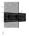
Adverting to FIG. 1, a method of forming a semiconductor device with wafer backside protection from copper contamination, in accordance with an exemplary embodiment, begins with a silicon substrate 100 including a TSV 101 surrounded by a protective film 103 and a passivation layer 105. As illustrated, the protective film 103 is contiguous with the TSV 101 and the passivation layer 105, and the passivation layer is contiguous with the silicon substrate 100. The TSV 101 may be made of any conductive metal, such as copper (Cu). The protective film 103 may be formed of tantalum (Ta) or tantalum nitride (TaN). The passivation layer 105 may be formed of tetraethyl orthosilicate (TEOS) or any other passivation material.
Next, as illustrated in FIG. 2, the method proceeds with backgrinding of the silicon substrate 100 down to approximately the passivation layer 105, followed by etching of the silicon substrate 100 to expose a bottom portion 201 of the TSV 101. The etching of the silicon substrate 100 may be accomplished using ammonium hydroxide (NH4OH), potassium hydroxide (KOH), or a combination thereof. After etching the silicon substrate 100, the bottom portion 201 of the TSV 101 may protrude 0.5 to 3 μm (e.g., 1 μm) from the bottom surface of the silicon substrate 100.
Next, an oxide layer 301 is formed over the bottom portion 201 of the TSV 101 and the bottom surface of the silicon substrate 100, as illustrated in FIG. 3. The oxide layer 301 may be formed of TEOS, a high aspect ratio oxide (HARP), amorphous hydrogenated carbon doped silicon oxide (SiCOH) and other doped silicon oxides. The oxide layer 301 may be formed to a thickness of 100 to 500 Å (e.g., 300 Å).
Adverting to FIG. 4, a silicon composite layer 401 is formed over the oxide layer 301. The silicon composite layer 401 may be formed of silicon nitride (SiN), silicon carbide (SiC), or a combination thereof at a thickness of 500 to 1000 Å (e.g., 750 Å). The silicon composite layer 401 may act as a backside contamination protection layer during the exposure of the TSV.
FIGS. 5A and 5B illustrate various embodiments for forming a hardmask layer 501 over the silicon composite layer 401. In both embodiments, the hardmask layer 501 may be formed to a thickness of 1 to 3 μm (e.g., 1 μm) and may be formed of TEOS.
As illustrated in FIG. 5A, the hardmask layer 501 may be deposited over the silicon composite layer 401. The hardmask layer 501 may be deposited according to any known deposition method, such as chemical vapor deposition. Subsequently, as illustrated in FIG. 6, a mask is created using the hardmask layer 501 by removing the hardmask layer 501 down to the silicon composite layer 401 over the bottom portion of the TSV 101, to expose a section 601 of the silicon composite layer 401. The hardmask layer 501 may then be planarized using a fixed abrasive, low selectivity chemical mechanical polish (CMP) slurry, such as CMP platen 2 to expose the section 601 of the silicon composite layer 401.
Adverting back to FIG. 5B, the hardmask layer 501 may instead be formed of a spin-on resist or a planarization film followed by a hard bake at 100 to 550° C. Subsequently, the mask of FIG. 6 may be created by removing the hardmask layer 501 down to the silicon composite layer 401 over the bottom portion 201 of the TSV 101 to expose the section 601 of the silicon composite layer 401 using a wet etch that removes TEOS. Alternatively, a combination of planarization and wet etching may be used.
Adverting to FIG. 7, the section 601 of the silicon composite layer 401 may be removed by wet etching, dry etching, or a combination thereof. For instance, the section 601 of the silicon composite layer 401 may be removed by a wet etch using phosphoric acid (H3PO4).
As illustrated in FIG. 8, the remaining hardmask layer 501, the exposed portion of the oxide layer 301, and a portion the passivation layer 105 may be removed by wet etching, dry etching, or a combination thereof to re-expose the bottom portion 201 of the TSV 101. However, unlike the first exposure illustrated in FIG. 2, the bottom portion 201 is exposed in FIG. 8 without the passivation layer 105. For instance, the remaining hardmask layer 501, the exposed portion of the oxide layer 301, and a portion the passivation layer 105 may be removed by a wet etch with dilute hydrofluoric acid (HF).
As shown in FIG. 8, the re-exposed bottom portion 201 of the TSV 101 may still include the protective film 103. Adverting to FIG. 9, the protective film 103 may be removed from the bottom surface of the re-exposed bottom portion 201 by CMP or other methods (e.g., RIE), to expose a contact 901 for the bottom portion 201 of the TSV 101.
The embodiments of the present disclosure achieve several technical effects, including preventing copper contamination at the backside of wafers during TSV exposure. Embodiments of the present disclosure enjoy utility in various industrial applications as, for example, microprocessors, smart phones, mobile phones, cellular handsets, set-top boxes, DVD recorders and players, automotive navigation, printers and peripherals, networking and telecom equipment, gaming systems, and digital cameras. The present disclosure therefore enjoys industrial applicability in any of various types of highly integrated semiconductor devices.
In the preceding description, the present disclosure is described with reference to specifically exemplary embodiments thereof. It will, however, be evident that various modifications and changes may be made thereto without departing from the broader spirit and scope of the present disclosure, as set forth in the claims. The specification and drawings are, accordingly, to be regarded as illustrative and not as restrictive. It is understood that the present disclosure is capable of using various other combinations and embodiments and is capable of any changes or modifications within the scope of the inventive concept as expressed herein.

Claims (17)

What is claimed is:
1. A device comprising:
a silicon substrate;
a silicon composite layer covering a bottom surface of the silicon substrate, the silicon composite layer having a bottom surface;
an exposed portion of a through silicon via (TSV) protruding out from the bottom surface of the silicon substrate and the bottom surface of the silicon composite layer;
a protective film and a passivation layer surrounding the TSV, between the TSV and the silicon substrate,
wherein the protective film is contiguous with the TSV, and only the protective film extends down sides of the exposed portion of the TSV below the bottom surface of the silicon composite layer.
2. The device according to claim 1, further comprising an oxide layer between the silicon substrate and the silicon composite layer.
3. The device according to claim 2, wherein the oxide layer is formed to a thickness of 100 angstroms (Å) to 500 Å.
4. The device according to claim 1, wherein the silicon composite layer comprises silicon nitride, silicon carbide, or a combination thereof.
5. The device according to claim 1, wherein the silicon composite layer is formed to a thickness of 500 Å to 1000 Å.
6. The device according to claim 1, wherein the exposed portion of the TSV protrudes 0.5 microns (μm) to 3 μm out from the bottom surface of the silicon substrate.
7. The device according to claim 1, wherein the passivation layer is contiguous with the silicon substrate and extends to the bottom surface of the silicon composite layer.
8. A device comprising:
a silicon substrate;
a silicon composite layer covering a bottom surface of the silicon substrate, the silicon composite layer having a bottom surface;
an oxide layer between the silicon composite layer and both the silicon substrate and the TSV;
an exposed portion of a through silicon via (TSV) protruding out from the bottom surface of the silicon substrate, the oxide layer and the bottom surface of the silicon composite layer; and
a protective film and a passivation layer surrounding the TSV, between the TSV and the silicon substrate,
wherein the protective film is contiguous with the TSV, and only the protective film extends down sides of the exposed portion of the TSV below the bottom surface of the silicon composite layer.
9. The device according to claim 8, wherein the oxide layer is formed to a thickness of 100 angstroms (Å) to 500 Å.
10. The device according to claim 8, wherein the silicon composite layer comprises silicon nitride, silicon carbide, or a combination thereof.
11. The device according to claim 8, wherein the silicon composite layer is formed to a thickness of 500 Å to 1000 Å.
12. The device according to claim 8, wherein the protective film comprises tantalum (Ta) or tantalum nitride (TaN).
13. The device according to claim 8, wherein the passivation layer is contiguous with the silicon substrate and extends to a bottom surface of the silicon composite layer.
14. The device according to claim 8, wherein the exposed portion of the TSV protrudes 0.5 microns (μm) to 3 μm out from the bottom surface of the silicon substrate.
15. A device comprising:
a silicon substrate;
a silicon composite layer covering a bottom surface of the silicon substrate, the silicon composite layer having a bottom surface;
an oxide layer between the silicon composite layer and both the silicon substrate and the TSV;
an exposed portion of a conductive through silicon via (TSV) protruding 0.5 microns (μm) to 3 μm out from the bottom surface of the silicon substrate, the oxide layer and the bottom surface of the silicon composite layer;
a protective film contiguous with the TSV, surrounding the TSV between the TSV and the silicon substrate; and
a passivation layer contiguous with the silicon substrate, surrounding the TSV between the TSV and the silicon substrate, and extending to a bottom surface of the silicon composite layer,
wherein only the protective film extends down sides of the exposed portion of the TSV below the bottom surface of the silicon composite layer.
16. The device according to claim 15, wherein the oxide layer is formed to a thickness of 100 angstroms (Å) to 500 Å.
17. The device according to claim 15, wherein the silicon composite layer is formed to a thickness of 500 Å to 1000 Å.
US14/575,639 2012-07-05 2014-12-18 Method for forming through silicon via with wafer backside protection Active US9230886B2 (en)

Priority Applications (1)

Application Number Priority Date Filing Date Title
US14/575,639 US9230886B2 (en) 2012-07-05 2014-12-18 Method for forming through silicon via with wafer backside protection

Applications Claiming Priority (2)

Application Number Priority Date Filing Date Title
US13/542,256 US8940637B2 (en) 2012-07-05 2012-07-05 Method for forming through silicon via with wafer backside protection
US14/575,639 US9230886B2 (en) 2012-07-05 2014-12-18 Method for forming through silicon via with wafer backside protection

Related Parent Applications (1)

Application Number Title Priority Date Filing Date
US13/542,256 Division US8940637B2 (en) 2012-07-05 2012-07-05 Method for forming through silicon via with wafer backside protection

Publications (2)

Publication Number Publication Date
US20150137359A1 US20150137359A1 (en) 2015-05-21
US9230886B2 true US9230886B2 (en) 2016-01-05

Family

ID=49877910

Family Applications (2)

Application Number Title Priority Date Filing Date
US13/542,256 Active 2032-10-23 US8940637B2 (en) 2012-07-05 2012-07-05 Method for forming through silicon via with wafer backside protection
US14/575,639 Active US9230886B2 (en) 2012-07-05 2014-12-18 Method for forming through silicon via with wafer backside protection

Family Applications Before (1)

Application Number Title Priority Date Filing Date
US13/542,256 Active 2032-10-23 US8940637B2 (en) 2012-07-05 2012-07-05 Method for forming through silicon via with wafer backside protection

Country Status (1)

Country Link
US (2) US8940637B2 (en)

Families Citing this family (3)

* Cited by examiner, † Cited by third party
Publication number Priority date Publication date Assignee Title
KR101840846B1 (en) * 2012-02-15 2018-03-21 삼성전자주식회사 Semicoductor devices having through vias and methods for fabricating the same
US9012324B2 (en) * 2012-08-24 2015-04-21 United Microelectronics Corp. Through silicon via process
KR102320821B1 (en) 2014-09-11 2021-11-02 삼성전자주식회사 Semiconductor package

Citations (21)

* Cited by examiner, † Cited by third party
Publication number Priority date Publication date Assignee Title
US20020115290A1 (en) * 2001-02-22 2002-08-22 Halahan Patrick B. Semiconductor structures having multiple conductive layers in an opening, and methods for fabricating same
US20030219939A1 (en) 2001-12-10 2003-11-27 Shahriar Ahmed Self aligned compact bipolar junction transistor layout and method of making same
US6734084B1 (en) 2003-02-04 2004-05-11 Mitsubishi Denki Kabushiki Kaisha Method of manufacturing a semiconductor device with recesses using anodic oxide
US20050029630A1 (en) 2003-03-25 2005-02-10 Yoshihide Matsuo Manufacturing method for semiconductor device, semiconductor device, and electronic apparatus
US20050151228A1 (en) 2003-12-04 2005-07-14 Kazumasa Tanida Semiconductor chip and manufacturing method for the same, and semiconductor device
US20070032061A1 (en) 2005-08-05 2007-02-08 Farnworth Warren M Methods of forming through-wafer interconnects and structures resulting therefrom
US7214615B2 (en) 2003-03-17 2007-05-08 Seiko Epson Corporation Method of manufacturing semiconductor device, semiconductor device, circuit substrate and electronic apparatus
US20090243047A1 (en) * 2008-04-01 2009-10-01 Andreas Wolter Semiconductor Device With an Interconnect Element and Method for Manufacture
US20100025852A1 (en) 2006-12-22 2010-02-04 Makoto Ueki Semiconductor device and method for manufacturing the same
US20100038800A1 (en) 2008-08-18 2010-02-18 Samsung Electronics Co., Ltd. Through-silicon via structures including conductive protective layers and methods of forming the same
US20100164117A1 (en) * 2008-12-31 2010-07-01 Ming-Fa Chen Through-Silicon Via With Air Gap
US20100178747A1 (en) * 2009-01-13 2010-07-15 Maxim Integrated Products, Inc. Minimum Cost Method for Forming High Density Passive Capacitors for Replacement of Discrete Board Capacitors Using a Minimum Cost 3D Wafer-to-Wafer Modular Integration Scheme
US7902643B2 (en) 2006-08-31 2011-03-08 Micron Technology, Inc. Microfeature workpieces having interconnects and conductive backplanes, and associated systems and methods
US20110095435A1 (en) 2009-10-28 2011-04-28 International Business Machines Corporation Coaxial through-silicon via
WO2012020689A1 (en) 2010-08-10 2012-02-16 国立大学法人東北大学 Method of manufacturing semiconductor device and semiconductor device
US20120061827A1 (en) * 2010-09-15 2012-03-15 Elpida Memory, Inc. Semiconductor device
US20120074584A1 (en) * 2010-09-27 2012-03-29 Samsung Electronics Co., Ltd. Multi-layer tsv insulation and methods of fabricating the same
US20120091520A1 (en) * 2010-10-15 2012-04-19 Elpida Memory, Inc. Semiconductor device, method for forming the same, and data processing system
US20130049127A1 (en) * 2011-08-24 2013-02-28 Taiwan Semiconductor Manufacturing Company, Ltd. Controlling the Device Performance by Forming a Stressed Backside Dielectric Layer
US20130113103A1 (en) * 2011-11-03 2013-05-09 Texas Instruments Incorporated DEVICE HAVING TSVs WITH GETTERING LAYER LATERAL TO TSV TIPS
US20130334699A1 (en) * 2012-06-19 2013-12-19 Chien-Li Kuo Semiconductor device and fabricating method thereof

Family Cites Families (9)

* Cited by examiner, † Cited by third party
Publication number Priority date Publication date Assignee Title
US8501587B2 (en) * 2009-01-13 2013-08-06 Taiwan Semiconductor Manufacturing Company, Ltd. Stacked integrated chips and methods of fabrication thereof
US9018684B2 (en) * 2009-11-23 2015-04-28 California Institute Of Technology Chemical sensing and/or measuring devices and methods
JP2011166106A (en) * 2010-01-13 2011-08-25 Renesas Electronics Corp Semiconductor device manufacturing method, and semiconductor device
US8896136B2 (en) * 2010-06-30 2014-11-25 Taiwan Semiconductor Manufacturing Company, Ltd. Alignment mark and method of formation
US8492878B2 (en) * 2010-07-21 2013-07-23 International Business Machines Corporation Metal-contamination-free through-substrate via structure
US8928159B2 (en) * 2010-09-02 2015-01-06 Taiwan Semiconductor Manufacturing & Company, Ltd. Alignment marks in substrate having through-substrate via (TSV)
JP5853389B2 (en) * 2011-03-28 2016-02-09 ソニー株式会社 Semiconductor device and manufacturing method of semiconductor device.
US8563403B1 (en) * 2012-06-27 2013-10-22 International Business Machines Corporation Three dimensional integrated circuit integration using alignment via/dielectric bonding first and through via formation last
US8709936B2 (en) * 2012-07-31 2014-04-29 International Business Machines Corporation Method and structure of forming backside through silicon via connections

Patent Citations (23)

* Cited by examiner, † Cited by third party
Publication number Priority date Publication date Assignee Title
US20020115290A1 (en) * 2001-02-22 2002-08-22 Halahan Patrick B. Semiconductor structures having multiple conductive layers in an opening, and methods for fabricating same
US20030219939A1 (en) 2001-12-10 2003-11-27 Shahriar Ahmed Self aligned compact bipolar junction transistor layout and method of making same
US6734084B1 (en) 2003-02-04 2004-05-11 Mitsubishi Denki Kabushiki Kaisha Method of manufacturing a semiconductor device with recesses using anodic oxide
US7214615B2 (en) 2003-03-17 2007-05-08 Seiko Epson Corporation Method of manufacturing semiconductor device, semiconductor device, circuit substrate and electronic apparatus
US20050029630A1 (en) 2003-03-25 2005-02-10 Yoshihide Matsuo Manufacturing method for semiconductor device, semiconductor device, and electronic apparatus
US20050151228A1 (en) 2003-12-04 2005-07-14 Kazumasa Tanida Semiconductor chip and manufacturing method for the same, and semiconductor device
US20070032061A1 (en) 2005-08-05 2007-02-08 Farnworth Warren M Methods of forming through-wafer interconnects and structures resulting therefrom
US7902643B2 (en) 2006-08-31 2011-03-08 Micron Technology, Inc. Microfeature workpieces having interconnects and conductive backplanes, and associated systems and methods
US20100025852A1 (en) 2006-12-22 2010-02-04 Makoto Ueki Semiconductor device and method for manufacturing the same
US20090243047A1 (en) * 2008-04-01 2009-10-01 Andreas Wolter Semiconductor Device With an Interconnect Element and Method for Manufacture
US20100038800A1 (en) 2008-08-18 2010-02-18 Samsung Electronics Co., Ltd. Through-silicon via structures including conductive protective layers and methods of forming the same
US20100164117A1 (en) * 2008-12-31 2010-07-01 Ming-Fa Chen Through-Silicon Via With Air Gap
US7910473B2 (en) 2008-12-31 2011-03-22 Taiwan Semiconductor Manufacturing Company, Ltd. Through-silicon via with air gap
US20100178747A1 (en) * 2009-01-13 2010-07-15 Maxim Integrated Products, Inc. Minimum Cost Method for Forming High Density Passive Capacitors for Replacement of Discrete Board Capacitors Using a Minimum Cost 3D Wafer-to-Wafer Modular Integration Scheme
US20110095435A1 (en) 2009-10-28 2011-04-28 International Business Machines Corporation Coaxial through-silicon via
WO2012020689A1 (en) 2010-08-10 2012-02-16 国立大学法人東北大学 Method of manufacturing semiconductor device and semiconductor device
US20130140700A1 (en) * 2010-08-10 2013-06-06 National University Corporation Tohoku University Method of manufacturing a semiconductor device and semiconductor device
US20120061827A1 (en) * 2010-09-15 2012-03-15 Elpida Memory, Inc. Semiconductor device
US20120074584A1 (en) * 2010-09-27 2012-03-29 Samsung Electronics Co., Ltd. Multi-layer tsv insulation and methods of fabricating the same
US20120091520A1 (en) * 2010-10-15 2012-04-19 Elpida Memory, Inc. Semiconductor device, method for forming the same, and data processing system
US20130049127A1 (en) * 2011-08-24 2013-02-28 Taiwan Semiconductor Manufacturing Company, Ltd. Controlling the Device Performance by Forming a Stressed Backside Dielectric Layer
US20130113103A1 (en) * 2011-11-03 2013-05-09 Texas Instruments Incorporated DEVICE HAVING TSVs WITH GETTERING LAYER LATERAL TO TSV TIPS
US20130334699A1 (en) * 2012-06-19 2013-12-19 Chien-Li Kuo Semiconductor device and fabricating method thereof

Non-Patent Citations (2)

* Cited by examiner, † Cited by third party
Title
K. Hozawa et al., "Impact of Backside Cu Contamination in the 3D Integration Process," 2009 Symposium on VLSI Technology Digest of Technical Papers, IEEE, 2009, pp. 172-173.
K. Lee et al., "Concerns of 3D Integration Technology Using TSV," Conference Publication, 6th Annual SEMATECH Symposium Japan, Sep. 13-15, 2010, 21 pages.

Also Published As

Publication number Publication date
US8940637B2 (en) 2015-01-27
US20140008810A1 (en) 2014-01-09
US20150137359A1 (en) 2015-05-21

Similar Documents

Publication Publication Date Title
TWI440088B (en) A first inter-layer dielectric stack for non-volatile memory
US9666791B2 (en) Topological method to build self-aligned MTJ without a mask
TWI405298B (en) Sti formation in semiconductor device including soi and bulk silicon regions
EP3731265B1 (en) Integrating through substrate vias into middle-of-line layers of integrated circuits
US20130119543A1 (en) Through silicon via for stacked wafer connections
US20160086874A1 (en) Semiconductor devices including through-silicon-vias and methods of manufacturing the same and semiconductor packages including the semiconductor devices
US9627215B1 (en) Structure and method for interconnection
US9257323B2 (en) Semiconductor device and method for forming the same
US9230886B2 (en) Method for forming through silicon via with wafer backside protection
US20080081433A1 (en) Method for Forming a Shallow Trench Isolation Structure
JP2013074275A (en) Semiconductor device manufacturing method
US8426291B2 (en) Method for isolation formation in manufacturing semiconductor device
US10522393B2 (en) Devices and methods of forming thereof by post single layer transfer fabrication of device isolation structures
US20150270159A1 (en) Fabrication of semiconductor structures using oxidized polycrystalline silicon as conformal stop layers
US20140213034A1 (en) Method for forming isolation structure
US9275874B2 (en) Methods for fabricating integrated circuits using chemical mechanical planarization to recess metal
US20140353728A1 (en) Method and apparatus for a reduced capacitance middle-of-the-line (mol) nitride stack
US9768064B1 (en) Formation method of semiconductor device structure
US8084364B2 (en) Method of fabricating semiconductor device
US20130217205A1 (en) Methods for fabricating semiconductor devices with isolation regions having uniform stepheights
US11773353B2 (en) Semiconductor device cleaning solution, method of use, and method of manufacture
US20240087950A1 (en) Wet etch process and methods to form air gaps between metal interconnects
US8987034B2 (en) Backside illumination CMOS image sensor and method of manufacturing the same
US20150087134A1 (en) Semiconductor isolation region uniformity
US8043932B2 (en) Method of fabricating semiconductor device

Legal Events

Date Code Title Description
FEPP Fee payment procedure

Free format text: PAYOR NUMBER ASSIGNED (ORIGINAL EVENT CODE: ASPN); ENTITY STATUS OF PATENT OWNER: LARGE ENTITY

AS Assignment

Owner name: GLOBALFOUNDRIES SINGAPORE PTE.LTD., SINGAPORE

Free format text: ASSIGNMENT OF ASSIGNORS INTEREST;ASSIGNORS:LEONG, LUP SAN;ZOU, ZHENG;HUNG SEE, ALEX KAI;AND OTHERS;SIGNING DATES FROM 20120704 TO 20120705;REEL/FRAME:037102/0628

STCF Information on status: patent grant

Free format text: PATENTED CASE

AS Assignment

Owner name: WILMINGTON TRUST, NATIONAL ASSOCIATION, DELAWARE

Free format text: SECURITY AGREEMENT;ASSIGNOR:GLOBALFOUNDRIES INC.;REEL/FRAME:049490/0001

Effective date: 20181127

MAFP Maintenance fee payment

Free format text: PAYMENT OF MAINTENANCE FEE, 4TH YEAR, LARGE ENTITY (ORIGINAL EVENT CODE: M1551); ENTITY STATUS OF PATENT OWNER: LARGE ENTITY

Year of fee payment: 4

AS Assignment

Owner name: GLOBALFOUNDRIES INC., CAYMAN ISLANDS

Free format text: RELEASE BY SECURED PARTY;ASSIGNOR:WILMINGTON TRUST, NATIONAL ASSOCIATION;REEL/FRAME:054636/0001

Effective date: 20201117

MAFP Maintenance fee payment

Free format text: PAYMENT OF MAINTENANCE FEE, 8TH YEAR, LARGE ENTITY (ORIGINAL EVENT CODE: M1552); ENTITY STATUS OF PATENT OWNER: LARGE ENTITY

Year of fee payment: 8