US9242855B2 - Bulk nano-ribbon and/or nano-porous structures for thermoelectric devices and methods for making the same - Google Patents
Bulk nano-ribbon and/or nano-porous structures for thermoelectric devices and methods for making the same Download PDFInfo
- Publication number
- US9242855B2 US9242855B2 US14/333,197 US201414333197A US9242855B2 US 9242855 B2 US9242855 B2 US 9242855B2 US 201414333197 A US201414333197 A US 201414333197A US 9242855 B2 US9242855 B2 US 9242855B2
- Authority
- US
- United States
- Prior art keywords
- nano
- ribbons
- portions
- semiconductor substrate
- another example
- Prior art date
- Legal status (The legal status is an assumption and is not a legal conclusion. Google has not performed a legal analysis and makes no representation as to the accuracy of the status listed.)
- Expired - Fee Related
Links
- 239000002074 nanoribbon Substances 0.000 title claims abstract description 291
- 238000000034 method Methods 0.000 title claims abstract description 209
- 239000000463 material Substances 0.000 claims description 134
- 239000000758 substrate Substances 0.000 claims description 129
- 239000004065 semiconductor Substances 0.000 claims description 108
- 230000008569 process Effects 0.000 claims description 100
- 238000005530 etching Methods 0.000 claims description 39
- 238000001039 wet etching Methods 0.000 claims description 22
- 238000000926 separation method Methods 0.000 claims description 19
- 238000007788 roughening Methods 0.000 claims description 18
- 238000003486 chemical etching Methods 0.000 claims description 16
- 239000011800 void material Substances 0.000 claims description 15
- 239000011343 solid material Substances 0.000 claims description 4
- 239000002086 nanomaterial Substances 0.000 description 86
- XUIMIQQOPSSXEZ-UHFFFAOYSA-N Silicon Chemical compound [Si] XUIMIQQOPSSXEZ-UHFFFAOYSA-N 0.000 description 32
- 229910052710 silicon Inorganic materials 0.000 description 28
- 239000010703 silicon Substances 0.000 description 28
- 238000010586 diagram Methods 0.000 description 24
- 229920001400 block copolymer Polymers 0.000 description 22
- 238000012986 modification Methods 0.000 description 22
- 230000004048 modification Effects 0.000 description 22
- 238000000059 patterning Methods 0.000 description 18
- 229910052709 silver Inorganic materials 0.000 description 16
- BQCADISMDOOEFD-UHFFFAOYSA-N Silver Chemical compound [Ag] BQCADISMDOOEFD-UHFFFAOYSA-N 0.000 description 15
- 239000002245 particle Substances 0.000 description 15
- 239000004332 silver Substances 0.000 description 15
- HBMJWWWQQXIZIP-UHFFFAOYSA-N silicon carbide Chemical compound [Si+]#[C-] HBMJWWWQQXIZIP-UHFFFAOYSA-N 0.000 description 13
- 229910010271 silicon carbide Inorganic materials 0.000 description 13
- 235000012431 wafers Nutrition 0.000 description 13
- 239000010408 film Substances 0.000 description 12
- 239000000178 monomer Substances 0.000 description 12
- SQGYOTSLMSWVJD-UHFFFAOYSA-N silver(1+) nitrate Chemical compound [Ag+].[O-]N(=O)=O SQGYOTSLMSWVJD-UHFFFAOYSA-N 0.000 description 12
- 235000014653 Carica parviflora Nutrition 0.000 description 11
- 241000243321 Cnidaria Species 0.000 description 11
- 239000010409 thin film Substances 0.000 description 11
- 229920002120 photoresistant polymer Polymers 0.000 description 9
- 238000009826 distribution Methods 0.000 description 8
- 238000004519 manufacturing process Methods 0.000 description 8
- 239000002070 nanowire Substances 0.000 description 7
- 230000008901 benefit Effects 0.000 description 6
- 239000002184 metal Substances 0.000 description 6
- 229910052751 metal Inorganic materials 0.000 description 6
- 238000010248 power generation Methods 0.000 description 6
- 230000015572 biosynthetic process Effects 0.000 description 5
- 210000004556 brain Anatomy 0.000 description 5
- 229920001577 copolymer Polymers 0.000 description 5
- 229910052802 copper Inorganic materials 0.000 description 4
- 239000010949 copper Substances 0.000 description 4
- 238000004146 energy storage Methods 0.000 description 4
- 239000002923 metal particle Substances 0.000 description 4
- 239000000203 mixture Substances 0.000 description 4
- 239000002904 solvent Substances 0.000 description 4
- 239000000126 substance Substances 0.000 description 4
- 230000003746 surface roughness Effects 0.000 description 4
- RYGMFSIKBFXOCR-UHFFFAOYSA-N Copper Chemical compound [Cu] RYGMFSIKBFXOCR-UHFFFAOYSA-N 0.000 description 3
- VYPSYNLAJGMNEJ-UHFFFAOYSA-N Silicium dioxide Chemical compound O=[Si]=O VYPSYNLAJGMNEJ-UHFFFAOYSA-N 0.000 description 3
- 238000003491 array Methods 0.000 description 3
- 238000006555 catalytic reaction Methods 0.000 description 3
- 238000006243 chemical reaction Methods 0.000 description 3
- 229910017052 cobalt Inorganic materials 0.000 description 3
- 239000010941 cobalt Substances 0.000 description 3
- GUTLYIVDDKVIGB-UHFFFAOYSA-N cobalt atom Chemical compound [Co] GUTLYIVDDKVIGB-UHFFFAOYSA-N 0.000 description 3
- 239000011521 glass Substances 0.000 description 3
- 239000011159 matrix material Substances 0.000 description 3
- 229910052755 nonmetal Inorganic materials 0.000 description 3
- 238000000206 photolithography Methods 0.000 description 3
- 238000005240 physical vapour deposition Methods 0.000 description 3
- 230000005678 Seebeck effect Effects 0.000 description 2
- 229910052581 Si3N4 Inorganic materials 0.000 description 2
- GWEVSGVZZGPLCZ-UHFFFAOYSA-N Titan oxide Chemical compound O=[Ti]=O GWEVSGVZZGPLCZ-UHFFFAOYSA-N 0.000 description 2
- XLOMVQKBTHCTTD-UHFFFAOYSA-N Zinc monoxide Chemical compound [Zn]=O XLOMVQKBTHCTTD-UHFFFAOYSA-N 0.000 description 2
- MCMNRKCIXSYSNV-UHFFFAOYSA-N Zirconium dioxide Chemical compound O=[Zr]=O MCMNRKCIXSYSNV-UHFFFAOYSA-N 0.000 description 2
- 239000004964 aerogel Substances 0.000 description 2
- 238000000231 atomic layer deposition Methods 0.000 description 2
- 230000009286 beneficial effect Effects 0.000 description 2
- 238000005229 chemical vapour deposition Methods 0.000 description 2
- 238000000151 deposition Methods 0.000 description 2
- 230000009977 dual effect Effects 0.000 description 2
- 230000005611 electricity Effects 0.000 description 2
- 238000000866 electrolytic etching Methods 0.000 description 2
- 229910052737 gold Inorganic materials 0.000 description 2
- 238000011065 in-situ storage Methods 0.000 description 2
- 239000012212 insulator Substances 0.000 description 2
- 239000002105 nanoparticle Substances 0.000 description 2
- 238000001020 plasma etching Methods 0.000 description 2
- 238000005086 pumping Methods 0.000 description 2
- HQVNEWCFYHHQES-UHFFFAOYSA-N silicon nitride Chemical compound N12[Si]34N5[Si]62N3[Si]51N64 HQVNEWCFYHHQES-UHFFFAOYSA-N 0.000 description 2
- 238000003631 wet chemical etching Methods 0.000 description 2
- -1 FeO2 Inorganic materials 0.000 description 1
- 229910001218 Gallium arsenide Inorganic materials 0.000 description 1
- 230000005679 Peltier effect Effects 0.000 description 1
- 239000004793 Polystyrene Substances 0.000 description 1
- 229910004541 SiN Inorganic materials 0.000 description 1
- 229910000577 Silicon-germanium Inorganic materials 0.000 description 1
- ATJFFYVFTNAWJD-UHFFFAOYSA-N Tin Chemical compound [Sn] ATJFFYVFTNAWJD-UHFFFAOYSA-N 0.000 description 1
- LEVVHYCKPQWKOP-UHFFFAOYSA-N [Si].[Ge] Chemical compound [Si].[Ge] LEVVHYCKPQWKOP-UHFFFAOYSA-N 0.000 description 1
- 229910052782 aluminium Inorganic materials 0.000 description 1
- PNEYBMLMFCGWSK-UHFFFAOYSA-N aluminium oxide Inorganic materials [O-2].[O-2].[O-2].[Al+3].[Al+3] PNEYBMLMFCGWSK-UHFFFAOYSA-N 0.000 description 1
- 239000013590 bulk material Substances 0.000 description 1
- 210000004027 cell Anatomy 0.000 description 1
- 229910000424 chromium(II) oxide Inorganic materials 0.000 description 1
- 238000004140 cleaning Methods 0.000 description 1
- 239000011248 coating agent Substances 0.000 description 1
- 238000000576 coating method Methods 0.000 description 1
- 229910052681 coesite Inorganic materials 0.000 description 1
- 238000001816 cooling Methods 0.000 description 1
- 229910052593 corundum Inorganic materials 0.000 description 1
- 230000008878 coupling Effects 0.000 description 1
- 238000010168 coupling process Methods 0.000 description 1
- 238000005859 coupling reaction Methods 0.000 description 1
- 229910052906 cristobalite Inorganic materials 0.000 description 1
- 239000013078 crystal Substances 0.000 description 1
- 230000003247 decreasing effect Effects 0.000 description 1
- 230000008021 deposition Effects 0.000 description 1
- 229920000359 diblock copolymer Polymers 0.000 description 1
- 239000002019 doping agent Substances 0.000 description 1
- 238000004070 electrodeposition Methods 0.000 description 1
- 230000002708 enhancing effect Effects 0.000 description 1
- 239000007789 gas Substances 0.000 description 1
- 229910052732 germanium Inorganic materials 0.000 description 1
- GNPVGFCGXDBREM-UHFFFAOYSA-N germanium atom Chemical compound [Ge] GNPVGFCGXDBREM-UHFFFAOYSA-N 0.000 description 1
- CJNBYAVZURUTKZ-UHFFFAOYSA-N hafnium(IV) oxide Inorganic materials O=[Hf]=O CJNBYAVZURUTKZ-UHFFFAOYSA-N 0.000 description 1
- UQSXHKLRYXJYBZ-UHFFFAOYSA-N iron oxide Inorganic materials [Fe]=O UQSXHKLRYXJYBZ-UHFFFAOYSA-N 0.000 description 1
- JEIPFZHSYJVQDO-UHFFFAOYSA-N iron(III) oxide Inorganic materials O=[Fe]O[Fe]=O JEIPFZHSYJVQDO-UHFFFAOYSA-N 0.000 description 1
- 238000011031 large-scale manufacturing process Methods 0.000 description 1
- 231100001231 less toxic Toxicity 0.000 description 1
- 239000007769 metal material Substances 0.000 description 1
- 150000002739 metals Chemical class 0.000 description 1
- 239000002106 nanomesh Substances 0.000 description 1
- 239000007800 oxidant agent Substances 0.000 description 1
- 230000000149 penetrating effect Effects 0.000 description 1
- 238000005191 phase separation Methods 0.000 description 1
- 229920003229 poly(methyl methacrylate) Polymers 0.000 description 1
- 239000004926 polymethyl methacrylate Substances 0.000 description 1
- 229920002223 polystyrene Polymers 0.000 description 1
- 238000011084 recovery Methods 0.000 description 1
- 230000009467 reduction Effects 0.000 description 1
- 238000005057 refrigeration Methods 0.000 description 1
- 238000010963 scalable process Methods 0.000 description 1
- 230000002000 scavenging effect Effects 0.000 description 1
- 239000000741 silica gel Substances 0.000 description 1
- 229910002027 silica gel Inorganic materials 0.000 description 1
- 239000000377 silicon dioxide Substances 0.000 description 1
- 239000002210 silicon-based material Substances 0.000 description 1
- 229910052682 stishovite Inorganic materials 0.000 description 1
- 210000000352 storage cell Anatomy 0.000 description 1
- 230000002194 synthesizing effect Effects 0.000 description 1
- PBCFLUZVCVVTBY-UHFFFAOYSA-N tantalum pentoxide Inorganic materials O=[Ta](=O)O[Ta](=O)=O PBCFLUZVCVVTBY-UHFFFAOYSA-N 0.000 description 1
- 239000013077 target material Substances 0.000 description 1
- 229910052718 tin Inorganic materials 0.000 description 1
- OGIDPMRJRNCKJF-UHFFFAOYSA-N titanium oxide Inorganic materials [Ti]=O OGIDPMRJRNCKJF-UHFFFAOYSA-N 0.000 description 1
- 229910052905 tridymite Inorganic materials 0.000 description 1
- 239000002918 waste heat Substances 0.000 description 1
- 229910001845 yogo sapphire Inorganic materials 0.000 description 1
Images


Classifications
-
- B—PERFORMING OPERATIONS; TRANSPORTING
- B81—MICROSTRUCTURAL TECHNOLOGY
- B81C—PROCESSES OR APPARATUS SPECIALLY ADAPTED FOR THE MANUFACTURE OR TREATMENT OF MICROSTRUCTURAL DEVICES OR SYSTEMS
- B81C1/00—Manufacture or treatment of devices or systems in or on a substrate
- B81C1/00436—Shaping materials, i.e. techniques for structuring the substrate or the layers on the substrate
- B81C1/00523—Etching material
- B81C1/00539—Wet etching
-
- B—PERFORMING OPERATIONS; TRANSPORTING
- B82—NANOTECHNOLOGY
- B82Y—SPECIFIC USES OR APPLICATIONS OF NANOSTRUCTURES; MEASUREMENT OR ANALYSIS OF NANOSTRUCTURES; MANUFACTURE OR TREATMENT OF NANOSTRUCTURES
- B82Y10/00—Nanotechnology for information processing, storage or transmission, e.g. quantum computing or single electron logic
-
- H—ELECTRICITY
- H01—ELECTRIC ELEMENTS
- H01L—SEMICONDUCTOR DEVICES NOT COVERED BY CLASS H10
- H01L21/00—Processes or apparatus adapted for the manufacture or treatment of semiconductor or solid state devices or of parts thereof
- H01L21/02—Manufacture or treatment of semiconductor devices or of parts thereof
- H01L21/04—Manufacture or treatment of semiconductor devices or of parts thereof the devices having at least one potential-jump barrier or surface barrier, e.g. PN junction, depletion layer or carrier concentration layer
- H01L21/18—Manufacture or treatment of semiconductor devices or of parts thereof the devices having at least one potential-jump barrier or surface barrier, e.g. PN junction, depletion layer or carrier concentration layer the devices having semiconductor bodies comprising elements of Group IV of the Periodic System or AIIIBV compounds with or without impurities, e.g. doping materials
- H01L21/30—Treatment of semiconductor bodies using processes or apparatus not provided for in groups H01L21/20 - H01L21/26
- H01L21/302—Treatment of semiconductor bodies using processes or apparatus not provided for in groups H01L21/20 - H01L21/26 to change their surface-physical characteristics or shape, e.g. etching, polishing, cutting
- H01L21/306—Chemical or electrical treatment, e.g. electrolytic etching
- H01L21/30604—Chemical etching
- H01L21/30608—Anisotropic liquid etching
-
- H—ELECTRICITY
- H01—ELECTRIC ELEMENTS
- H01L—SEMICONDUCTOR DEVICES NOT COVERED BY CLASS H10
- H01L21/00—Processes or apparatus adapted for the manufacture or treatment of semiconductor or solid state devices or of parts thereof
- H01L21/02—Manufacture or treatment of semiconductor devices or of parts thereof
- H01L21/04—Manufacture or treatment of semiconductor devices or of parts thereof the devices having at least one potential-jump barrier or surface barrier, e.g. PN junction, depletion layer or carrier concentration layer
- H01L21/18—Manufacture or treatment of semiconductor devices or of parts thereof the devices having at least one potential-jump barrier or surface barrier, e.g. PN junction, depletion layer or carrier concentration layer the devices having semiconductor bodies comprising elements of Group IV of the Periodic System or AIIIBV compounds with or without impurities, e.g. doping materials
- H01L21/30—Treatment of semiconductor bodies using processes or apparatus not provided for in groups H01L21/20 - H01L21/26
- H01L21/302—Treatment of semiconductor bodies using processes or apparatus not provided for in groups H01L21/20 - H01L21/26 to change their surface-physical characteristics or shape, e.g. etching, polishing, cutting
- H01L21/306—Chemical or electrical treatment, e.g. electrolytic etching
- H01L21/308—Chemical or electrical treatment, e.g. electrolytic etching using masks
- H01L21/3083—Chemical or electrical treatment, e.g. electrolytic etching using masks characterised by their size, orientation, disposition, behaviour, shape, in horizontal or vertical plane
- H01L21/3085—Chemical or electrical treatment, e.g. electrolytic etching using masks characterised by their size, orientation, disposition, behaviour, shape, in horizontal or vertical plane characterised by their behaviour during the process, e.g. soluble masks, redeposited masks
-
- H—ELECTRICITY
- H01—ELECTRIC ELEMENTS
- H01L—SEMICONDUCTOR DEVICES NOT COVERED BY CLASS H10
- H01L29/00—Semiconductor devices adapted for rectifying, amplifying, oscillating or switching, or capacitors or resistors with at least one potential-jump barrier or surface barrier, e.g. PN junction depletion layer or carrier concentration layer; Details of semiconductor bodies or of electrodes thereof ; Multistep manufacturing processes therefor
- H01L29/02—Semiconductor bodies ; Multistep manufacturing processes therefor
- H01L29/06—Semiconductor bodies ; Multistep manufacturing processes therefor characterised by their shape; characterised by the shapes, relative sizes, or dispositions of the semiconductor regions ; characterised by the concentration or distribution of impurities within semiconductor regions
- H01L29/0657—Semiconductor bodies ; Multistep manufacturing processes therefor characterised by their shape; characterised by the shapes, relative sizes, or dispositions of the semiconductor regions ; characterised by the concentration or distribution of impurities within semiconductor regions characterised by the shape of the body
- H01L29/0665—Semiconductor bodies ; Multistep manufacturing processes therefor characterised by their shape; characterised by the shapes, relative sizes, or dispositions of the semiconductor regions ; characterised by the concentration or distribution of impurities within semiconductor regions characterised by the shape of the body the shape of the body defining a nanostructure
- H01L29/0669—Nanowires or nanotubes
- H01L29/0673—Nanowires or nanotubes oriented parallel to a substrate
-
- H—ELECTRICITY
- H01—ELECTRIC ELEMENTS
- H01L—SEMICONDUCTOR DEVICES NOT COVERED BY CLASS H10
- H01L29/00—Semiconductor devices adapted for rectifying, amplifying, oscillating or switching, or capacitors or resistors with at least one potential-jump barrier or surface barrier, e.g. PN junction depletion layer or carrier concentration layer; Details of semiconductor bodies or of electrodes thereof ; Multistep manufacturing processes therefor
- H01L29/66—Types of semiconductor device ; Multistep manufacturing processes therefor
- H01L29/66007—Multistep manufacturing processes
- H01L29/66075—Multistep manufacturing processes of devices having semiconductor bodies comprising group 14 or group 13/15 materials
- H01L29/66227—Multistep manufacturing processes of devices having semiconductor bodies comprising group 14 or group 13/15 materials the devices being controllable only by the electric current supplied or the electric potential applied, to an electrode which does not carry the current to be rectified, amplified or switched, e.g. three-terminal devices
- H01L29/66409—Unipolar field-effect transistors
- H01L29/66439—Unipolar field-effect transistors with a one- or zero-dimensional channel, e.g. quantum wire FET, in-plane gate transistor [IPG], single electron transistor [SET], striped channel transistor, Coulomb blockade transistor
-
- H01L35/32—
-
- H01L35/34—
-
- H—ELECTRICITY
- H10—SEMICONDUCTOR DEVICES; ELECTRIC SOLID-STATE DEVICES NOT OTHERWISE PROVIDED FOR
- H10N—ELECTRIC SOLID-STATE DEVICES NOT OTHERWISE PROVIDED FOR
- H10N10/00—Thermoelectric devices comprising a junction of dissimilar materials, i.e. devices exhibiting Seebeck or Peltier effects
- H10N10/01—Manufacture or treatment
-
- H—ELECTRICITY
- H10—SEMICONDUCTOR DEVICES; ELECTRIC SOLID-STATE DEVICES NOT OTHERWISE PROVIDED FOR
- H10N—ELECTRIC SOLID-STATE DEVICES NOT OTHERWISE PROVIDED FOR
- H10N10/00—Thermoelectric devices comprising a junction of dissimilar materials, i.e. devices exhibiting Seebeck or Peltier effects
- H10N10/10—Thermoelectric devices comprising a junction of dissimilar materials, i.e. devices exhibiting Seebeck or Peltier effects operating with only the Peltier or Seebeck effects
- H10N10/17—Thermoelectric devices comprising a junction of dissimilar materials, i.e. devices exhibiting Seebeck or Peltier effects operating with only the Peltier or Seebeck effects characterised by the structure or configuration of the cell or thermocouple forming the device
Definitions
- the present invention is directed to nanostructures. More particularly, the invention provides bulk nano-ribbon and/or nano-porous structures. Merely by way of example, the invention has been applied to thermoelectric devices. However, it would be recognized that the invention has a much broader range of applicability, including but not limited to use in transistor, solar power converter, battery electrodes and/or energy storage, catalysis, and/or light emitting diodes.
- thermoelectric figures of merit ZT Conventional nanostructure devices, such as nanohole and nanomesh devices, have been shown to have good thermoelectric figures of merit ZT.
- ZT S 2 ⁇ /k, where S is the material's thermopower, a is the electrical conductivity, and k is the thermal conductivity.
- S the material's thermopower
- a the electrical conductivity
- k the thermal conductivity.
- These devices have been formed in thin silicon-on-insulator epitaxial layers or formed from arrays of nanowires, and result in nanoscale structures in thin films that are very small in physical size.
- some conventional silicon nanoholes have been fabricated from a thin silicon film of 10-1000 nm within a conventional silicon wafer, whereby the remainder of the silicon wafer that is about 500 ⁇ m thick is etched and discarded.
- Fabrication of certain nanostructures includes formation of nanowires and nanoholes from a single piece of material.
- certain block copolymer patterning techniques are known for nano-scaled surface patterning.
- certain nanostructures have an aspect ratio of over 100:1 with feature size of several tens of nanometers to hundreds of nanometers.
- Low cost material like silicon is a target material for forming such nanostructures for the manufacture of high-performance thermoelectrics. It has been shown that silicon nanowires with low thermal conductivity can be fabricated using low cost, scalable process, but demonstrating certain difficulty in forming good electrical contacts with all nanowires.
- silicon nanoholes or holey silicon structures also are characterized by low thermal conductivity and being easier to form electrical contacts.
- the present invention is directed to nanostructures. More particularly, the invention provides bulk nano-ribbon and/or nano-porous structures. Merely by way of example, the invention has been applied to thermoelectric devices. However, it would be recognized that the invention has a much broader range of applicability, including but not limited to use in transistor, solar power converter, battery electrodes and/or energy storage, catalysis, and/or light emitting diodes.
- a structure including nano-ribbons include multiple nano-ribbons.
- Each of the multiple nano-ribbons corresponds to a first end and a second end, and the first end and the second end are separated by a first distance of at least 100 ⁇ m.
- Each of the multiple nano-ribbons corresponds to a cross-sectional area associated with a ribbon thickness, and the ribbon thickness ranges from 5 nm to 500 nm.
- Each of the multiple nano-ribbons is separated from at least another nano-ribbon selected from the multiple nano-ribbons by a second distance ranging from 5 nm to 500 nm.
- a method for making a structure including nano-ribbons includes providing a semiconductor substrate including a first surface.
- the first surface includes first portions and second portions. Additionally, the method includes forming one or more layers on the first portions of the first surface. The second portions of the first surface are exposed. Moreover, the method includes etching the semiconductor substrate through the second portions of the first surface to form at least multiple nano-ribbons.
- Each of the nano-ribbons corresponds to a first end and a second end, and the first end and the second end are separated by a first distance of at least 100 ⁇ m.
- Each of the nano-ribbons corresponds to a cross-sectional area associated with a ribbon thickness ranging from 5 nm to 500 nm, and each of the nano-ribbons is separated from at least another nano-ribbon selected from the multiple nano-ribbons by a second distance ranging from 5 nm to 500 nm.
- a method for making a structure including one or more nano-ribbons includes providing a semiconductor substrate including a first surface.
- the first surface includes first portions and second portions. Additionally, the method includes forming one or more layers on the first portions of the first surface. The second portions of the first surface are exposed. Moreover, the method includes etching the semiconductor substrate through the second portions of the first surface to form at least one nano-ribbon including multiple nano-ribbon parts.
- Each of the nano-ribbon parts corresponds to a first end and a second end, and the first end and the second end are separated by a first distance of at least 100 ⁇ m.
- Each of the nano-ribbon parts corresponds to a cross-sectional area associated with a thickness ranging from 5 nm to 500 nm.
- Each of the nano-ribbon parts is separated from at least another nano-ribbon part selected from the multiple nano-ribbon parts by a second distance ranging from 5 nm to 500 nm.
- a method for making a porous structure includes providing a nonporous semiconductor substrate including one or more surfaces.
- the one or more surfaces include first portions and second portions. Additionally, the method includes forming one or more layers on the first portions of the one or more surfaces. The second portions of the one or more surfaces are exposed. Moreover, the method includes etching the nonporous semiconductor substrate through the second portions of the one or more surfaces to form a porous semiconductor substrate including multiple first voids connected with each other.
- Each of the multiple first voids corresponds to a first cross-sectional area associated with a first distance across ranging from 5 nm to 500 nm, and each of the multiple first voids are separated from at least another void by a first distance ranging from 5 nm to 500 nm.
- FIG. 1 is a simplified diagram showing a bulk nanostructure including one or more fill materials and bounded by electrode structures for forming a thermoelectric device structure according to one embodiment of the present invention.
- FIG. 2 is a simplified diagram showing a top view of the bulk nanostructure as part of the thermoelectric device structure according to one embodiment of the present invention.
- FIGS. 3A-3F are simplified diagrams each showing a top view of the bulk nanostructure as part of the thermoelectric device structure according to certain embodiments of the present invention.
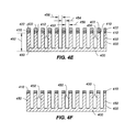
- FIGS. 4A-4F are simplified diagrams showing a method for making the bulk nanostructure as shown in FIG. 1 , FIG. 2 , FIG. 3A , FIG. 3B , FIG. 3C , FIG. 3D , FIG. 3E , and/or FIG. 3F according to certain embodiments of the present invention.
- FIG. 5 is a simplified diagram showing a process for roughening sidewalls of the multiple nano-ribbons as a part of the method for making the bulk nanostructure as shown in FIG. 1 , FIG. 2 , FIG. 3A , FIG. 3B , FIG. 3C , FIG. 3D , FIG. 3E , and/or FIG. 3F according to some embodiments of the present invention.
- FIG. 6 is a simplified diagram showing a process for forming nanoholes in sidewalls through the multiple nano-ribbons as a part of the method for making the bulk nanostructure as shown in FIG. 1 , FIG. 2 , FIG. 3A , FIG. 3B , FIG. 3C , FIG. 3D , FIG. 3E , and/or FIG. 3F according to some embodiments of the present invention.
- FIGS. 7A-7B are simplified diagrams showing a process for filling voids of a bulk nano-structure that includes the nano-ribbons with a block copolymer material as a part of the method for making the bulk nanostructure as shown in FIG. 1 , FIG. 2 , FIG. 3A , FIG. 3B , FIG. 3C , FIG. 3D , FIG. 3E , and/or FIG. 3F according to some embodiments of the present invention.
- FIGS. 8A-8B are simplified diagrams showing a process for etching the nano-ribbons to form nanoholes in the sidewalls through the nano-ribbons as a part of the method for making the bulk nanostructure as shown in FIG. 1 , FIG. 2 , FIG. 3A , FIG. 3B , FIG. 3C , FIG. 3D , FIG. 3E , and/or FIG. 3F according to some embodiments of the present invention.
- the present invention is directed to nanostructures. More particularly, the invention provides bulk nano-ribbon and/or nano-porous structures. Merely by way of example, the invention has been applied to thermoelectric devices. However, it would be recognized that the invention has a much broader range of applicability, including but not limited to use in transistor, solar power converter, battery electrodes and/or energy storage, catalysis, and/or light emitting diodes.
- thermoelectric devices may be transistors, thermoelectrics, or other electronic devices.
- a bulk nanostructure thermoelectric device used for power generation should transport a significant amount of electric current from one electrode to another, where a temperature gradient is applied to the thermoelectric material and the Seebeck effect is employed to generate a gradient in voltage and in turn the flow of electrical current.
- a bulk nanostructure thermoelectric device used for refrigeration should carry an appreciable amount of heat with an applied electric current by way of the Peltier effect.
- ZT of the thermoelectric material is one indicator of the material's efficiency in either converting heat to electricity (e.g., thermopower) or pumping heat with electricity.
- electrodes in a bulk nanostructure thermoelectric device, should be placed on either ends of the thermoelectric material in order to collect a current from the thermoelectric material or transmit a current through the thermoelectric material.
- these electrodes should be made such that the electrodes make low resistance electrical and thermal contact to the thermoelectric material with high ZT, and furthermore allow each thermoelectric unit of p-type or n-type semiconductor thermoelectric material (e.g., each thermoelectric leg) to be wired together with one or more other thermoelectric units and/or the external circuitry.
- the interesting applications for bulk nanohole thermoelectric device include heat energy scavenging for powering sensors, Peltier cooling of electronics hot-spots, and waste-heat recovery from exhaust and other heat sources, among others.
- heat energy scavenging for powering sensors
- Peltier cooling of electronics hot-spots for detecting waste-heat recovery from exhaust and other heat sources.
- waste-heat recovery from exhaust and other heat sources among others.
- in order for a bulk nanohole thermoelectric device to be usefully applied to one or more of these applications not only should suitable electrodes be made on the thermoelectric material, but an appreciable amount of the thermoelectric material itself should be fabricated to meet the geometrical and electrical specifications of the application.
- thermoelectric power generation from a heat source using the Seebeck effect enough volume of thermoelectric material should be present between a hot junction and a cold junction (e.g., in a counter-flow gas phase heat exchanger) so as to allow both an appreciable temperature gradient to evolve across thermoelectric legs and to allow enough current to be carried due to the temperature-induced voltage.
- thermoelectric material fabricated with small outer dimensions such as the conventional structures demonstrated incorporating nanoholes with relative short lengths, usually suffer from very high current densities that may preclude their use in a thermoelectric application. Furthermore, such thermoelectric structure often may not generate sufficient power or heat pumping that is applicable or cost-effective. Hence, the ability to process nanostructures for making high-performance thermoelectric devices would have signification cost advantages, if the nanostructures are fabricated with methods that are compatible with the processing of silicon and other semiconductor wafers, according to some embodiments.
- thermoelectric generation power density, ⁇ of such a device in a load-matched condition, where the temperature gradient is applied in the z direction, is:
- I is the current in the sample-load circuit
- R internal is the internal resistance of the thermoelectric material
- R load is the resistance of the load
- R is the sum of R internal and R load .
- A is the x-y cross-sectional area of the thermoelectric material that is orthogonal to the temperature gradient applied in the z direction
- V is the voltage generated by the thermoelectric material
- ⁇ is the electrical resistivity of the thermoelectric material.
- L x , L y , and L z are the sample dimensions in the x, y, and z directions respectively.
- the thermoelectric power can increase if the voltage generated by the sample is larger or if the electrical resistance of the sample is lower according to one embodiment.
- the voltage generated by the sample can be increased by selecting a thermoelectric material with a larger Seebeck coefficient S (e.g., S is equal to dV/dT).
- the electrical resistance of the sample can be lowered by decreasing the sample length L z along the axis of the temperature gradient and/or selecting a thermoelectric material with lower resistivity.
- the total amount of power P produced by the thermoelectric material sample, rather than the power density is then:
- thermoelectric sample that is larger in lateral x and y dimensions can produce more power, because there would be more thermoelectric material participating in the generation of voltage from an applied temperature gradient, and therefore more current generated.
- thermoelectric power generation becomes problematic if a thermoelectric device is made from a thin thermoelectric film where the direction of thermal and electrical transport is in the x-y plane of the thin film, and not in the z direction.
- thermoelectric thin film For a conventional thermoelectric thin film with nanoholes within it, the temperature gradient often needs to be applied in a direction that is orthogonal to the z direction of the thin film so as to take advantage of the beneficial effects of the nanohole structure within the material. But, in such an arrangement, a very small amount of thermoelectric material usually can contribute to the thermoelectric conversion. For example, if the temperature gradient is applied in they direction, referring to Equation 2, the transverse area (e.g., the cross-sectional area that is exposed to a temperature gradient through which a current may flow) is no longer L x ⁇ L y , but instead is equal to L x ⁇ L z , where z is the cross-plane direction (e.g., thickness direction) of the thin film.
- the transverse area e.g., the cross-sectional area that is exposed to a temperature gradient through which a current may flow
- thermoelectric conversion would be significantly restricted in terms of the amount of electric power it can generate according to one embodiment.
- P is linearly proportional to the transverse area, going from a thin film thicknesses of 100 nm to greater than 100 ⁇ m would increase power generation by about 1000 times.
- thermoelectric nanostructures when fabricating thermoelectric nanostructures from a finite wafer of material or the like, it is desirable to transform as much of the starting wafer material as possible into the thermoelectric nanostructures according to some embodiments.
- the commercial performance, and thus usefulness, of a power generation thermoelectric device is governed by its cost-per-Watt, it is beneficial to process a piece of material in such a fashion that maximizes its use as a thermoelectric material, because most of the two-dimensional semiconductor fabrication processes or the like usually cost about the same amount regardless of the thickness of the material being processed.
- a bulk-like structure that can combine advantages of both the nanohole structure and the ultra-long nanowire structure, featuring both ultra low thermal conductivity and strong mechanical stiffness at far greater thickness ranges than those for thin-film holey silicon structures in order to achieve significant commercial applicability according to some embodiments.
- techniques for the formation of very large or bulk-like nano-ribbon and/or nano-porous structures combining certain desirable characteristics of nanowires and holey structures are implemented based on silicon and/or other less expensive and/or less toxic semiconductor materials.
- methods are also provided for synthesizing the bulk nano-ribbon and/or nano-porous structures and making electrical contacts as their corresponding hot electrodes and/or cold electrodes to form one or more thermoelectric legs.
- FIG. 1 is a simplified diagram showing a bulk nanostructure including one or more fill materials and bounded by electrode structures for forming a thermoelectric device structure according to one embodiment of the present invention.
- the thermoelectric device structure 100 includes a bulk nanostructure 110 and electrode structures 120 and 122 .
- the bulk nanostructure 110 includes a bulk nano-ribbon structure and/or a bulk nano-porous structure.
- the bulk nanostructure 110 has a length L, a width W, and a height H, all of which are in macroscopic scale.
- each of the length L, the width W, and the height H is greater than a few millimeters, or greater than a few centimeters, or greater than tens of centimeters and greater.
- the bulk nanostructure 110 includes multiple nano-ribbons 130 that form parts of the bulk nano-ribbon structure or the bulk nano-porous structure.
- the multiple nano-ribbons 130 are substantially parallel to each other.
- the nano-ribbons 130 have nanoholes in their sidewalls (e.g., one or more roughened sidewalls and/or one or more un-roughened sidewalls) respectively, and form parts of the bulk nano-porous structure.
- the nano-ribbons 130 do not have multiple nanoholes in their sidewalls (e.g., one or more roughened sidewalls and/or one or more un-roughened sidewalls), and form parts of the bulk nano-ribbon structure.
- the nano-ribbons 130 each have one or more roughened sidewalls with surface roughness in nanometer scale.
- the bulk nanostructure 110 also includes one or more fill materials 140 that fill all the void spacing between the nano-ribbons 130 .
- each of the multiple nano-ribbons 130 is larger than 10 ⁇ m, larger than 100 ⁇ m, larger than 250 ⁇ m, larger than 400 ⁇ m, or larger than 500 ⁇ m.
- the thickness of each of the multiple nano-ribbons 130 ranges from 5 nm to 500 nm.
- each of the multiple nano-ribbons 130 is separated from another nano-ribbon 130 by spatial separation (e.g., a pitch distance) ranging from 5 nm to 500 nm.
- the bulk nanostructure 110 also includes one or more fill materials 140 .
- the nano-ribbons 130 are partially or completely separated from each other by voids.
- one or more of the voids are completely surrounded by one or more solid materials of the bulk nanostructure 110 .
- one or more of the voids are open to an area outside the bulk nanostructure 110 .
- the voids are filled with the one or more fill materials 140 .
- the one or more fill materials 140 also fill the nanoholes within the nano-ribbons 130 .
- the one or more fill materials 140 form a matrix (e.g., a porous matrix).
- the one or more fill materials 140 have a low thermal conductivity.
- the one or more fill materials 140 also have a low electrical conductivity.
- the thermal conductivity is between 0.0001 W/(m ⁇ K) and 50 W/(m ⁇ K).
- the one or more fill materials 140 have a low coefficient of thermal expansion.
- the linear coefficient of thermal expansion is between 0.01 ⁇ m/m ⁇ K and 30 ⁇ m/m ⁇ K.
- the one or more fill materials 140 are able to withstand temperatures in excess of 350° C. for extended periods of device operation. In yet another example, the one or more fill materials 140 are able to withstand temperatures in excess of 550° C. for extended periods of device operation. In yet another example, the one or more fill materials 140 are able to withstand temperatures in excess of 650° C. for extended periods of device operation. In yet another example, the one or more fill materials 140 are able to withstand temperatures in excess of 750° C. In yet another example, the one or more fill materials 140 are able to withstand temperatures in excess of 800° C.
- the one or more fill materials 140 provide added mechanical stability to the nano-ribbons 130 .
- the one or more fill materials 140 are able to be planarized.
- the one or more fill materials 140 are able to be polished.
- the one or more fill materials 140 provide a support base for additional material overlying thereon.
- the one or more fill materials 140 support the formation of good electrical contacts with the nano-ribbons 130 .
- the one or more fill materials 140 support the formation of good thermal contacts with the nano-ribbons 130 .
- the one or more fill materials 140 each include at least one selected from a group consisting of photoresist, spin-on glass, spin-on dopant, aerogel, xerogel, and oxide, and the like.
- the photoresist includes long UV wavelength G-line (e.g., approximately 436 nm) photoresist.
- the photoresist has negative photoresist characteristics.
- the photoresist exhibits good adhesion to various substrate materials, including Si, GaAs, InP, and glass.
- the photoresist exhibits good adhesion to various metals, including Au, Cu, and Al.
- the spin-on glass has a high dielectric constant.
- the aerogel is derived from silica gel characterized by an extremely low thermal conductivity of about 0.1 W/(m ⁇ K) and lower.
- the one or more fill materials 140 include long chains of one or more oxides.
- the oxide includes Al 2 O 3 , FeO, FeO 2 , Fe 2 O 3 , TiO, TiO 2 , ZrO 2 , ZnO, HfO 2 , CrO, Ta 2 O 5 , SiN, TiN, BN, SiO 2 , AN, CN, and/or the like.
- the bulk nanostructure 110 is sandwiched between the electrode structures 120 and 122 .
- the bulk nanostructure 110 is in electrical contact with each of the electrode structures 120 and 122 .
- each of the electrode structures 120 and 122 includes one or more thermal and electrical contact materials, serving as both an electrode and a thermal terminal.
- the electrode structures 120 and 122 are set at two different temperatures, and provide a temperature gradient across the bulk nanostructure 110 .
- the bulk nanostructure 110 is made from a bulk semiconductor substrate for forming one or more electronic devices such as transistors, solar cells, thermoelectric elements, battery/energy storage cells, and/or light emitting diodes.
- a pure or doped crystal silicon substrate is used to form the bulk nanostructure 110 .
- the top portion and/or the bottom portion of the bulk nanostructure 110 made from the bulk semiconductor substrate, after filled with a low thermal conductivity and low electrical conductivity fill material, can be flattened for coupling thermally and electrically to the electrode structures 120 and 122 respectively.
- the electrode structures 120 and 122 can serve as a hot electrode and a cold electrode respectively, for forming a thermoelectric element.
- the thermoelectric element can be used as a building block to form one or more high efficiency thermoelectric devices.
- the multiple nano-ribbons 130 are parts of a thermoelectric device.
- the multiple nano-ribbons 130 are replaced by at least a nano-ribbon that is folded into multiple nano-ribbons parts and includes the multiple nano-ribbons parts.
- the multiple nano-ribbons 130 are arranged in a pattern comprising multiple isolated or partially connected fins as shown in FIG. 2 .
- the pattern is configured to enlarge sidewall areas for all fins.
- FIG. 2 is a simplified diagram showing a top view of the bulk nanostructure 110 as part of the thermoelectric device structure 100 according to one embodiment of the present invention. This diagram is merely an example, which should not unduly limit the scope of the claims. One of ordinary skill in the art would recognize many variations, alternatives, and modifications.
- the bulk nanostructure 110 includes multiple nano-ribbons 130 that form parts of a bulk nano-ribbon structure or a bulk nano-porous structure.
- the nano-ribbons 130 have nanoholes in their sidewalls respectively, and form parts of the bulk nano-porous structure.
- the nano-ribbons 130 do not have multiple nanoholes in their sidewalls, and form parts of the bulk nano-ribbon structure.
- the nano-ribbons 130 are separated, partially or completely, by voids 200 .
- the voids 200 are filled with the one or more fill materials 140 .
- the nano-ribbons 130 are roughly 50/50 interlaced with the voids 200 to form a coral pattern or structure (e.g., a brain coral pattern or structure, a coral pattern or structure in nanometer scale).
- the multiple nano-ribbons 130 are formed by vertically extending the voids 200 with the coral pattern, resulting in substantial sidewall surface areas for the multiple nano-ribbons 130 , according to some embodiments.
- the multiple nano-ribbons 130 with the coral pattern is substantially interconnected, leading to an enhanced mechanical stiffness.
- each fin of the multiple nano-ribbons 130 has an average side-wall thickness of 1000 nm or less, and is separated, partially or completely, from a neighboring fin by a pitch size ranging from 100 nm to 20000 nm.
- each fin of the multiple nano-ribbons 130 has an average side-wall thickness ranging from 5 nm to 500 nm, and is separated, partially or completely, from a neighboring fin by a pitch size ranging from 5 nm to 500 nm.
- the coral pattern of the nano-ribbons 130 with nanoscale separations are created by applying one or more block copolymers over a silicon carbide hard mask overlying a silicon substrate.
- the one or more block copolymers are made up of blocks of different polymerized monomers that undergo a phase separation.
- multiple blocks of one or more block copolymers are covalently bonded to each other, so these blocks do not demix macroscopically due to incompatibility between the blocks.
- each block depending on the relative lengths of each block, several morphologies can be obtained. For example, in diblock copolymers, sufficiently different block lengths lead to nanometer-sized spheres of one monomer in a matrix of another monomer (e.g., PMMA in polystyrene). In another example, using less different block lengths, a hexagonally packed cylinder geometry can be obtained. In yet another example, blocks of similar block lengths can form one or more layers (e.g., one or more lamellae). In yet another example, between the cylindrical phase and the lamellar phase, there is the three-dimensional gyroid phase.
- a hexagonally packed cylinder geometry can be obtained.
- blocks of similar block lengths can form one or more layers (e.g., one or more lamellae). In yet another example, between the cylindrical phase and the lamellar phase, there is the three-dimensional gyroid phase.
- the nanoscale structures created from block copolymers could also potentially be used for creating devices for use in computer memory and/or nanoscale-templating.
- FIG. 2 is merely an example, which should not unduly limit the scope of the claims.
- the volumes corresponding to the voids 200 become the nano-ribbons 130
- the volumes corresponding to the nano-ribbons 130 become the voids 200 .
- FIGS. 3A-3F are simplified diagrams each showing a top view of the bulk nanostructure 110 as part of the thermoelectric device structure 100 according to certain embodiments of the present invention. These diagrams are merely examples, which should not unduly limit the scope of the claims. One of ordinary skill in the art would recognize many variations, alternatives, and modifications.
- the multiple nano-ribbons 130 each have a straight shape, and the multiple nano-ribbons 130 are substantially parallel with each other in the top view according to one embodiment.
- the nano-ribbons 130 are separated, partially or completely, by voids 310 .
- the voids 310 are filled with the one or more fill materials 140 .
- FIG. 3A is merely an example, which should not unduly limit the scope of the claims.
- the nano-ribbons 130 do not have a constant width.
- the spacing e.g., the width of a void 310
- the volumes corresponding to the voids 310 become the nano-ribbons 130
- the volumes corresponding to the nano-ribbons 130 become the voids 310 .
- the multiple nano-ribbons 130 each have a curved shape, and the multiple nano-ribbons 130 are substantially parallel with each other in the top view according to another embodiment.
- the nano-ribbons 130 are separated, partially or completely, by voids 320 .
- the voids 320 are filled with the one or more fill materials 140 .
- FIG. 3B is merely an example, which should not unduly limit the scope of the claims.
- the nano-ribbons 130 do not have a constant width.
- the spacing e.g., the width of a void 320
- the volumes corresponding to the voids 320 become the nano-ribbons 130
- the volumes corresponding to the nano-ribbons 130 become the voids 320 .
- the multiple nano-ribbons 130 are organized into two fin structures 332 and 334 in the top view according to yet another embodiment.
- the fin structures 332 and 334 each include multiple fingers.
- the fingers of the fin structure 332 extend toward to the fin structure 334
- the fingers of the fin structure 334 extend toward to the fin structure 332 , with shifted spacing and mutual separation.
- the nano-ribbons 130 are separated, partially or completely, by voids 330 .
- the voids 330 are filled with the one or more fill materials 140 .
- FIG. 3C is merely an example, which should not unduly limit the scope of the claims.
- the nano-ribbons 130 do not have a constant width.
- the spacing e.g., the width of a void 330
- the volumes corresponding to the voids 330 become the nano-ribbons 130
- the volumes corresponding to the nano-ribbons 130 become the voids 330 .
- the multiple nano-ribbons 130 are organized into one or more honeycomb patterns in the top view according to yet another embodiment.
- the nano-ribbons 130 are separated, partially or completely, by voids 340 .
- the voids 340 are filled with the one or more fill materials 140 .
- FIG. 3D is merely an example, which should not unduly limit the scope of the claims.
- the nano-ribbons 130 do not have a constant width.
- the spacing between two of the nano-ribbons 130 is not constant.
- the multiple nano-ribbons 130 are organized into one or more Sierpinsky Curve patterns in the top view according to yet another embodiment.
- the nano-ribbons 130 are separated, partially or completely, by voids 350 .
- the voids 350 are filled with the one or more fill materials 140 .
- FIG. 3E is merely an example, which should not unduly limit the scope of the claims.
- the nano-ribbons 130 do not have a constant length or a constant width.
- the spacing between two of the nano-ribbons 130 is not constant.
- the volumes corresponding to the voids 350 become the nano-ribbons 130
- the volumes corresponding to the nano-ribbons 130 become the voids 350 .
- the multiple nano-ribbons 130 are organized into one or more Hilbert Curve patterns in the top view according to yet another embodiment.
- the nano-ribbons 130 are separated, partially or completely, by voids 360 .
- the voids 360 are filled with the one or more fill materials 140 .
- FIG. 3F is merely an example, which should not unduly limit the scope of the claims.
- the nano-ribbons 130 do not have a constant length or a constant width.
- the spacing between two of the nano-ribbons 130 is not constant.
- the volumes corresponding to the voids 360 become the nano-ribbons 130
- the volumes corresponding to the nano-ribbons 130 become the voids 360 .
- FIGS. 2 and 3 A- 3 F are merely examples, which should not unduly limit the scope of the claims.
- the multiple nano-ribbons 130 are replaced by at least a nano-ribbon that is folded into multiple nano-ribbons parts and includes the multiple nano-ribbons parts.
- the multiple nano-ribbons 130 are organized into one or more other two-dimensional fractal patterns with nanoscale separations in the top view.
- the one or more two-dimensional fractal patterns are formed using block copolymer patterning with various block monomer composition and/or using photolithography.
- the one or more two-dimensional fractal patterns are selected for their large boundary lengths in the top view in order to form the nano-ribbons 130 with enhanced stiffness.
- the bulk nanostructure 110 with more regular shaped patterns as shown in FIGS. 3A-3C can be made using conventional photolithography technique as part of the fabrication method, and such fabrication method should be comparable in cost for high volume manufacturing.
- FIGS. 4A-4F are simplified diagrams showing a method for making the bulk nanostructure 110 as shown in FIG. 1 , FIG. 2 , FIG. 3A , FIG. 3B , FIG. 3C , FIG. 3D , FIG. 3E , and/or FIG. 3F according to certain embodiments of the present invention.
- These diagrams are merely examples, which should not unduly limit the scope of the claims.
- One of ordinary skill in the art would recognize many variations, alternatives, and modifications.
- the method for making the bulk nanostructure 110 includes the following sequential processes (a) through (f):
- a substrate 400 (e.g., a nonporous semiconductor substrate) is provided for making the bulk nanostructure 110 .
- the substrate 400 includes a substrate surface 402 .
- the substrate 400 is a silicon substrate (e.g., a silicon wafer).
- the silicon substrate is doped into an n-type semiconductor or a p-type semiconductor with desired doping density.
- the silicon substrate is pre-treated to reduce the total thickness of the silicon substrate to about 500 ⁇ m to 600 ⁇ m.
- the silicon substrate is prepared to have the clean surface 402 suitable for subsequent processes.
- a mask layer 410 (e.g., a hard mask layer) is formed on the substrate surface 402 of the substrate 400 .
- the mask layer 410 includes silicon carbide.
- the silicon carbide layer 410 is coated on the substrate surface 402 by chemical vapor deposition, electro-coating, and/or physical vapor deposition (PVD).
- PVD physical vapor deposition
- the wide energy band gap of silicon carbide makes silicon carbide a good intermediate material for forming a semiconductor-metal contact.
- the mask layer 410 includes silver.
- the silver layer 410 is plated on the substrate surface 402 .
- the silver layer 410 after a nano-patterning process, can be directly utilized for deep etch into the substrate 400 (e.g., the silicon substrate 400 ) using metal-assisted chemical etching technique.
- a patterning layer 420 is formed on the mask layer 410 .
- the patterning layer 420 is made from a block copolymer material including two monomers corresponding to two different phases respectively.
- the patterning layer 420 includes blocks 422 of one of the two monomers, and blocks 424 of the other of the two monomers.
- the blocks 422 and 424 depending on the composition of these two monomers in the block copolymer material, there are certain spatial distributions for the blocks 422 and 424 .
- the blocks 422 have a width 426 ranging from 5 nm to 500 nm
- the blocks 424 have a width 428 ranging from 5 nm to 500 nm.
- the blocks 424 can be removed using a solvent that is selected to chemically react specifically with the blocks 424 while retaining the blocks 422 .
- the removal of the blocks 424 would expose corresponding portions of the mask layer 410 in a patterned distribution across the substrate 400 (e.g., across a bulk-sized range up to a whole wafer surface).
- the patterned distribution includes nanoscale pattern features (e.g., the blocks 422 ) and nanoscale separations between the pattern features (e.g., the blocks 422 ).
- the patterned distribution has an overall pattern size in a bulk dimension ranging from a few millimeters up to the whole wafer surface.
- the blocks 424 of the patterning layer 420 are removed, and then the exposed portions of the mask layer 410 are also removed.
- the removal of the blocks 424 exposes the corresponding portions of the mask layer 410 in a patterned distribution across the substrate 400 , and then this patterned distribution with predetermined nanoscale separations is transferred to the mask layer 410 .
- the removal of the blocks 422 is performed by a wet etching process using a solvent that is selected to chemically react specifically with the blocks 424 while retaining the blocks 422 .
- the removal of the exposed portions of the mask layer 410 is performed by a plasma etching process.
- the corresponding regions of the substrate surface 402 are exposed.
- the block copolymer material including the two monomers with a 50/50 ratio is used to form the patterning layer 422 in order to create a pattern having a feature size (e.g., the width 426 ) of about 1000 nm or less and a pitch size (e.g., the width 428 ) ranging from 100 nm to 20000 nm.
- the created pattern has a feature size (e.g., the width 426 ) ranging from 5 nm to 500 nm, and a pitch size (e.g., the width 428 ) ranging from 5 nm to 500 nm.
- a photoresist material is formed overlying the mask layer 410 .
- a predetermined pattern with nanoscale separations between the pattern-features is created by photolithography (e.g., including a photomasking process, a light or electron exposure process, and a resist removal process).
- the predetermined pattern is transferred to the mask layer 410 , exposing the corresponding regions of the substrate surface 402 .
- portions of the substrate 400 are removed through the exposed regions of the substrate surface 402 .
- the exposed substrate material e.g., the exposed silicon material
- the exposed substrate material is etched to form multiple nano-ribbons 450 .
- the multiple nano-ribbons 450 are separated by one or more voids left behind by the removed portions of the substrate 400 .
- the multiple nano-ribbons 450 are substantially perpendicular to the substrate surface 402 .
- the multiple nano-ribbons 450 bear the same pattern deeply into the substrate 400 (e.g., the silicon substrate 400 ).
- the etching process includes a wet etching process (e.g., an electroless silver-assisted chemical etch and/or an electrolytic chemical etch).
- the etchant solution includes AgNO 3 , HF, and H 2 O 2 .
- the etching process is substantially uni-directional as the Ag nano-particles deposited on the exposed regions of the substrate surface 402 guide the chemical reaction in anisotropic fashion to form the nano-ribbons 450 with a height 452 .
- the etching process is controlled to extend the height of each of the multiple nano-ribbons 450 substantially vertically into the substrate 400 .
- each of the nano-ribbons 450 is characterized by a thickness 454 through its height 452 and a pitch distance 456 from its neighbor.
- the height 452 is larger than 10 ⁇ m.
- the height 452 is larger than 100 ⁇ m.
- the height 452 is larger than 250 ⁇ m.
- the height 452 is larger than 400 ⁇ m.
- the height 452 is larger than 500 ⁇ m.
- the height 452 is equal to the total thickness of the substrate 400 .
- the height 452 of the multiple nano-ribbons 450 are controlled to be within a small variation range, forming a relative flat bottom region that has a lateral dimension substantially equal to that of the original pattern defined by the nano-patterning process on the mask layer 410 .
- the thickness 454 of the multiple nano-ribbons 450 is substantially copied from that original pattern.
- the thickness 454 ranges from 5 nm to 500 nm.
- the thickness 454 is about 300 nm or less.
- the pitch distance 456 ranges from 5 nm to 500 nm.
- the pitch distance 456 ranges from 100 nm to 200 nm.
- the patterning layer 422 is removed from the mask layer 410 .
- the removal of the patterning layer 422 is performed after a cleaning process following etching the substrate as shown in FIG. 4E .
- the multiple nano-ribbons 450 are formed with nanoscale separations over a bulk sized range.
- the multiple nano-ribbons 450 are parts of a thermoelectric device.
- the multiple nano-ribbons 450 are the multiple nano-ribbons 130 as shown in FIG. 1 , FIG. 2 , FIG. 3A , FIG. 3B , FIG. 3C , FIG. 3D , FIG. 3E , and/or FIG. 3F .
- the method for making the bulk nanostructure 110 includes, after the processes (a) through (f), certain post treatment processes for substantially reducing thermal conductivity of the bulk nanostructure 110 in order to build a thermoelectric element with high thermoelectric figures of merit ZT.
- the method for making the bulk nanostructure 110 includes, after the processes (a) through (f), a process for filling the one or more voids (e.g., one or more separate regions) between the multiple nano-ribbons 450 with one or more fill materials (e.g., the one or more fill materials 140 ).
- the method for making the bulk nanostructure 110 includes, after the processes (a) through (f), a process for roughening sidewalls of the multiple nano-ribbons as shown in FIG. 5 .
- the method for making the bulk nanostructure 110 includes, after the processes (a) through (f), a process for forming nanoholes in sidewalls through the multiple nano-ribbons as shown in FIG. 6 .
- the method for making the bulk nanostructure 110 includes, after the processes (a) through (f), a process for roughening sidewalls of the multiple nano-ribbons as shown in FIG. 5 , and then a process for forming nanoholes in sidewalls through the multiple nano-ribbons as shown in FIG. 6 .
- FIG. 5 is a simplified diagram showing a process for roughening sidewalls of the multiple nano-ribbons as a part of the method for making the bulk nanostructure 110 as shown in FIG. 1 , FIG. 2 , FIG. 3A , FIG. 3B , FIG. 3C , FIG. 3D , FIG. 3E , and/or FIG. 3F according to some embodiments of the present invention.
- This diagram is merely an example, which should not unduly limit the scope of the claims.
- One of ordinary skill in the art would recognize many variations, alternatives, and modifications.
- each of the multiple nano-ribbons 450 includes one or more sidewalls 510 , and the one or more sidewalls 510 are roughened.
- the roughened sidewalls 510 of the multiple nano-ribbons 450 are provided by one or more etching processes (e.g., one or more silicon etching processes) using chemical wet etching and/or metal catalyzed etching.
- the roughened sidewalls 510 of the multiple nano-ribbons 450 are formed using electrolytic etching with impressed electrical current as well as HF solution and one or more oxidizers.
- the roughened sidewalls 510 of the multiple nano-ribbons 450 are formed by depositing either silicon or silicon germanium particles using chemical vapor deposition, physical vapor deposition, and/or atomic layer deposition. In yet another example, the roughened sidewalls 510 of the multiple nano-ribbons 450 are formed by in-situ thermal growth of a film (e.g., a silicon nitride film) partially over the sidewalls 510 with desired nano-roughness for each of the multiple nano-ribbons 450 .
- a film e.g., a silicon nitride film
- the resulting surface roughness is in nanometer scale and smaller than the thickness 454 of the corresponding nano-ribbon 450 .
- the resulting surface roughness added to each sidewall further contributes to the reduction of thermal conductivity across the bulk nanostructure 110 .
- throughout the sidewalls 510 for all the multiple nano-ribbons 450 multiple trenches and/or bumps in nanometer scale are formed, causing enhanced phonon scattering and reduced thermal conduction through the bulk nanostructure 110 .
- the multiple nano-ribbons 450 are parts of a thermoelectric device.
- the multiple nano-ribbons 450 are the multiple nano-ribbons 130 as shown in FIG. 1 , FIG. 2 , FIG. 3A , FIG. 3B , FIG. 3C , FIG. 3D , FIG. 3E , and/or FIG. 3F .
- the method for making the bulk nanostructure 110 includes, after the process for roughening sidewalls of the multiple nano-ribbons as shown in FIG. 5 , a process for filling the one or more voids (e.g., one or more separate regions) between the multiple nano-ribbons 450 with one or more fill materials (e.g., the one or more fill materials 140 ).
- FIG. 6 is a simplified diagram showing a process for forming nanoholes in sidewalls through the multiple nano-ribbons as a part of the method for making the bulk nanostructure 110 as shown in FIG. 1 , FIG. 2 , FIG. 3A , FIG. 3B , FIG. 3C , FIG. 3D , FIG. 3E , and/or FIG. 3F according to some embodiments of the present invention.
- This diagram is merely an example, which should not unduly limit the scope of the claims.
- One of ordinary skill in the art would recognize many variations, alternatives, and modifications.
- each of the multiple nano-ribbons 450 includes one or more sidewalls 510 , and in each of the one or more sidewalls 510 , multiple nanoholes 610 are generated through the corresponding nano-ribbons 450 .
- the substrate 400 e.g., a nonporous semiconductor substrate
- the porous substrate e.g., a porous semiconductor substrate
- each of the nanoholes 610 corresponds to a cross-sectional area associated with a distance across, and the distance across ranges from 5 nm to 500 nm.
- each nanohole 610 is separated from at least another nanohole 610 by a distance ranging from 5 nm to 500 nm.
- the process for forming nanoholes in sidewalls through the multiple nano-ribbons includes the following sequential processes (i) through (ii):
- FIGS. 7A-7B are simplified diagrams showing a process for filling voids of a bulk nano-structure that includes the nano-ribbons 450 with a block copolymer material as a part of the method for making the bulk nanostructure 110 as shown in FIG. 1 , FIG. 2 , FIG. 3A , FIG. 3B , FIG. 3C , FIG. 3D , FIG. 3E , and/or FIG. 3F according to some embodiments of the present invention.
- These diagrams are merely examples, which should not unduly limit the scope of the claims.
- One of ordinary skill in the art would recognize many variations, alternatives, and modifications.
- the voids of a bulk nano-structure that includes the nano-ribbons 450 are filled with a block copolymer material.
- the block copolymer material covers the sidewalls 510 of the nano-ribbons 450 .
- the block copolymer material is selected to produce a cylinder morphology with one monomer phase being impregnated with silver element from AgNO 3 as shown in FIG. 7B , but another monomer phase of the block copolymer material contains no silver element. Afterwards, the monomer phase of the block copolymer material that contains no silver element is removed by a properly selected solvent.
- the remaining portions of the block copolymer material is annealed in order to eliminate the non-metal components but leaving silver particles in nanometer scale on the sidewalls 510 of the nano-ribbons 450 according to one embodiment.
- the silver particles are disposed substantially uniformly throughout each of the sidewalls 510 (e.g., with hexagonal distribution on each of the sidewalls 510 ).
- FIGS. 8A-8B are simplified diagrams showing a process for etching the nano-ribbons to form nanoholes in the sidewalls through the nano-ribbons as a part of the method for making the bulk nanostructure 110 as shown in FIG. 1 , FIG. 2 , FIG. 3A , FIG. 3B , FIG. 3C , FIG. 3D , FIG. 3E , and/or FIG. 3F according to some embodiments of the present invention.
- These diagrams are merely examples, which should not unduly limit the scope of the claims.
- One of ordinary skill in the art would recognize many variations, alternatives, and modifications.
- an etchant solution including HF and oxidizer is used to electrolessly etch the nano-ribbons 450 from the corresponding sidewalls 510 , catalyzed by the silver particles, in order to form the multiple nanoholes 610 through the nano-ribbons 450 .
- the nano-ribbons 450 having the nanoholes 610 stand alone on the remaining portion of the substrate 400 , as shown in FIG. 8B .
- the multiple nano-ribbons 450 with the nanoholes 610 form parts of a bulk nano-porous structure characterized by a ribbon thickness and a sidewall separation both in the nanometer scale (e.g., in the order of 100 nanometers or greater) and further characterized by the nanoholes also in the nanometer scale (e.g., in the order of tens of nanometers) through the nano-ribbons 450 .
- the process for forming nanoholes in sidewalls through the multiple nano-ribbons is performed using a wet etching process based on an etchant including AgNO 3 and HF.
- an etchant including AgNO 3 and HF For example, a diluted AgNO 3 solution is used.
- the process for forming nanoholes in sidewalls through the multiple nano-ribbons is performed using wet chemical etching assisted by metal particles other than silver particles.
- metal particles other than silver particles For example, copper particles and/or cobalt particles are used to replace silver particles, and the copper particles and/or cobalt particles can help to form more dispersed nano-particles in the sidewalls 510 than the silver particles.
- the wet chemical etching can automatically accomplish desired size and desired spacing of metal particles (e.g., copper particles and/or cobalt particles) for etching the nanoholes 610 at corresponding locations within the sidewalls 510 of the nano-ribbons 450 .
- metal particles e.g., copper particles and/or cobalt particles
- the method for making the bulk nanostructure is simple and inexpensive. According to some embodiments, the method for making the bulk nanostructure is easily scalable. According to some embodiment, the bulk nanostructure (e.g., the bulk nano-ribbon structure and/or the nano-porous structure) has very low thermal conductivity that is nearly approaching to the amorphous limit of a bulk material in the same macroscopic size. For example, the bulk nanostructure (e.g., the bulk nano-ribbon structure and/or the nano-porous structure) starts from a flat top region of a bulk semiconductor substrate and ends at a relatively flat bottom region on the remaining portion of the substrate.
- the bulk nanostructure e.g., the bulk nano-ribbon structure and/or the nano-porous structure
- the nano-ribbons are configured to be substantially interconnected, greatly enhancing mechanical stiffness of the whole bulk nano-structure (e.g., the bulk nano-ribbon structure and/or the nano-porous structure) having about 500 ⁇ m in height comparing to arrays of individually standing nanowires in the similar height.
- the bottom region of the bulk nano-structure e.g., the bulk nano-ribbon structure and/or the nano-porous structure
- Such process can simplify fabrication of the thermoelectric device element (e.g., as shown in FIG. 1 ) and/or fabrication of a thermoelectric device with greatly enhanced large-volume manufacturability, according to some embodiments.
- Certain embodiments of the present invention provide a bulk nanostructure comprising a plurality of shaped ribbons vertically formed into a semiconductor substrate and laterally extended to any dimension up to the size of the semiconductor substrate.
- the plurality of shaped ribbons is characterized by a two-dimensional cross-sectional pattern featuring a ribbon thickness of 1000 nm or less and a pitch spacing ranging from 100 nm to 20000 nm and a substantially uniform height (or depth) exceeding 10 micrometers between a top region and a bottom region.
- the top region corresponds to a starting surface of the semiconductor substrate.
- the bottom region corresponds to end regions of all shaped ribbons that are rooted at remaining portion of the semiconductor substrate.
- the two-dimensional cross-sectional pattern of the plurality of shaped ribbons is one selected from, but not limited to, substantially a brain coral pattern, a honeycomb pattern, a Sierpinsky Curve pattern, a Hilbert Curve pattern, and a fractal pattern.
- the plurality of shaped ribbons is formed as parallel arrays of strait or curved fins.
- the plurality of shaped ribbons is formed as interconnected fins.
- the bulk nanostructure is characterized by nano-scale roughness throughout surfaces of the shaped ribbons so that the effective surface area is substantially enlarged.
- trenches and/or bumps having about a few tens of nanometers in depths or heights are formed across surfaces of the shaped ribbons.
- a plurality of nanometer-scaled holes with certain level of porosity e.g., ranging from about 30% to 90%
- distribute e.g., randomly distribute
- Some embodiments of the present invention provide a method for forming a bulk nanostructure (e.g., a bulk nano-ribbon structure, a bulk nano-ribbon structure) that includes a plurality of ribbons vertically arranged in a predetermined pattern with a bulk-like lateral dimension and a height greater than 10 ⁇ m on a semiconductor substrate.
- the plurality of ribbons is characterized by a group of fin structures with a wall thickness of about 1000 nm or less, a pitch distance ranging from about 100 nm to 20000 nm between neighboring fins, and a plurality of porous structural elements with nanometer-scaled feature sizes distributed throughout each fin.
- the method includes preparing the semiconductor substrate (e.g., a silicon wafer) by coating a silicon carbide film overlying the surface of the substrate. Furthermore, the method includes applying a patterning material overlying the silicon carbide film based on the predetermined nano-scale pattern.
- the predetermined nano-scale pattern is a pattern having its boundary length maximized or at least substantially enlarged in nanometer scale.
- the pattern is a brain coral structure with a feature thickness of 1000 nm or less and a pitch distance ranging from about 100 nm to 20000 nm distributed (e.g., uniformly distributed) across a bulk-sized lateral dimension ranging from a few millimeters to up to the whole surface of the substrate.
- the patterning material can be a block copolymer with roughly 50/50 dual-phase mixture.
- One of the dual phases can be easily removed by performing a chemical wet process to expose the silicon carbide mask film under the removed phase portions of the copolymer (e.g., exposing the silicon carbide mask film according to the brain coral structure), with the other of the dual phases remaining on the silicon carbide mask film.
- the method includes performing plasma etching to further remove the exposed portions of the silicon carbide film under the removed phase portions of the copolymer, with other portions of the silicon carbide film still covered by the other phase portions of the copolymer, exposing only corresponding portions of the semiconductor substrate.
- the method further includes etching the semiconductor material (e.g., silicon) into the semiconductor substrate under the exposed portions of the semiconductor substrate.
- the electroless metal-assisted chemical etching is used to remove the semiconductor material uni-directionally down to a depth into the semiconductor substrate.
- the depth can be greater than 10 ⁇ m.
- the depth is greater than 200 ⁇ m, or greater than 400 ⁇ m, or greater than 500 ⁇ m, or up to the total thickness of the semiconductor substrate.
- the remaining portions of the semiconductor substrate covered by the remaining portions of the silicon carbide film form a plurality of ribbons bearing the predetermined nano-scale pattern.
- the lateral dimension of the remaining portions of the semiconductor substrate after etching determines the ribbon thickness.
- the height or depth of the remaining portions of the semiconductor substrate after etching determines the height of the bulk nanostructure.
- the nano-ribbons are organized according to a brain coral pattern with nano-scale ribbon thickness (e.g., 1000 nm or less) and pitch distance (e.g., ranging from about 100 nm to 200 nm).
- the overall lateral spatial range of the pattern can be any specified bulk-size up to the whole substrate dimension (e.g., the whole wafer dimension).
- the method further includes a post-roughening process to create a plurality of trench and/or bump features throughout sidewalls of the plurality of ribbons.
- the trench and/or bump features e.g., about a few tens of nanometers or greater in their feature sizes and spacing
- the method includes a post-holing process to create a plurality of holes partially or completely penetrating the ribbon thickness of the plurality of ribbons.
- the plurality of holes distributed with a pitch distance (e.g., less than 100 nm) throughout the whole sidewall area of each ribbon can be formed by using a block copolymer hole patterning and a subsequent two-step etching process.
- the two-step etching process includes a first step to remove non-metal-containing phase of the copolymer using a selected solvent and to deposit the metal particles to the sidewalls of ribbons that are distributed according to a morphology pre-determined by the copolymer composition.
- the second step is to perform chemical etching that is assisted by the deposited metal particles on the sidewalls of the ribbons to cause holes formation in lateral directions partially or completely through the ribbon thickness.
- the metal material used in the above metal-assisted chemical etching is chosen from Ag, Au, or Co. Since the lateral dimension of the plurality of ribbons can have any bulk size ranging from a few millimeters up to the whole substrate dimension (e.g., the whole wafer dimension), a bulk nanostructure structure is formed by either the roughened ribbons (e.g., as parts of the bulk nano-ribbon structure) or the ribbons with nanoholes in sidewalls (e.g., as parts of the bulk nano-porous structure).
- a nanostructure e.g., a nano-ribbon structure, a nano-porous structure
- the nanostructure includes a plurality of ribbons arranged in a pattern with feature dimensions and separations in nanometer scales and each ribbon further being configured to bear nanometer surface roughness on its one or more sidewalls and/or nanometer-sized holes in its one or more sidewalls.
- the plurality of ribbons is formed substantially vertically into a bulk substrate in one or more of various patterns with substantial large surface areas.
- a method for forming such bulk nanostructure is provided.
- the bulk nanostructure has very low thermal conductivity and strong mechanical stiffness for fabricating high performance thermoelectric elements and corresponding devices.
- a structure including nano-ribbons include multiple nano-ribbons.
- Each of the multiple nano-ribbons corresponds to a first end and a second end, and the first end and the second end are separated by a first distance of at least 100 ⁇ m.
- Each of the multiple nano-ribbons corresponds to a cross-sectional area associated with a ribbon thickness, and the ribbon thickness ranges from 5 nm to 500 nm.
- Each of the multiple nano-ribbons is separated from at least another nano-ribbon selected from the multiple nano-ribbons by a second distance ranging from 5 nm to 500 nm.
- the structure is implemented according to at least FIG. 1 , FIG. 2 , FIG. 3A , FIG. 3B , FIG. 3C , FIG. 3D , FIG. 3E , and/or FIG. 3F .
- each of the multiple nano-ribbons includes one or more semiconductor materials.
- the one or more semiconductor materials are doped.
- the one or more semiconductor materials are silicon.
- each of the multiple nano-ribbons is separated from at least another nano-ribbon selected from the multiple nano-ribbons by one or more separation regions associated with the second distance.
- the one or more separation regions are filled with one or more fill materials.
- each of the multiple nano-ribbons includes one or more semiconductor materials different from the one or more fill materials.
- all of the multiple nano-ribbons are substantially parallel to each other.
- each of the multiple nano-ribbons corresponds to the first end at a first surface and is substantially perpendicular to the first surface.
- the cross-sectional area is substantially uniform along a height direction for each of the multiple nano-ribbons.
- the multiple nano-ribbons are parts of a thermoelectric device.
- the first distance is at least 250 ⁇ m.
- the first distance is at least 400 ⁇ m.
- the first distance is at least 500 ⁇ m.
- the multiple nano-ribbons include multiple roughened sidewall surfaces respectively.
- the multiple nano-ribbons include multiple nanoholes through corresponding nano-ribbons in corresponding sidewalls respectively.
- the multiple nano-ribbons further include multiple roughened sidewall surfaces respectively.
- a structure including one or more nano-ribbons includes a nano-ribbon including multiple nano-ribbon parts.
- Each of the multiple nano-ribbon parts corresponding to a first end and a second end, and the first end and the second end are separated by a first distance of at least 100 ⁇ m.
- Each of the multiple nano-ribbon parts corresponds to a cross-sectional area associated with a thickness, and the thickness ranging from 5 nm to 500 nm.
- Each of the multiple nano-ribbon parts is separated from at least another nano-ribbon part selected from the multiple nano-ribbon parts by a second distance ranging from 5 nm to 500 nm.
- the structure is implemented according to at least FIG. 1 , FIG. 2 , FIG. 3A , FIG. 3B , FIG. 3C , FIG. 3D , FIG. 3E , and/or FIG. 3F .
- each of the multiple nano-ribbon parts includes one or more semiconductor materials.
- the one or more semiconductor materials are doped.
- the one or more semiconductor materials are silicon.
- each of the multiple nano-ribbon parts is separated from at least another nano-ribbon part selected from the multiple nano-ribbon parts by one or more separation regions associated with the second distance.
- the one or more separation regions are filled with one or more fill materials.
- each of the multiple nano-ribbon parts includes one or more semiconductor materials different from the one or more fill materials.
- all of the multiple nano-ribbon parts are substantially parallel to each other.
- each of the multiple nano-ribbon parts corresponds to the first end at a first surface and is substantially perpendicular to the first surface.
- the cross-sectional area is substantially uniform along a height direction for each of the multiple nano-ribbon parts.
- the multiple nano-ribbon parts are parts of a thermoelectric device.
- the first distance is at least 250 ⁇ m.
- the first distance is at least 400 ⁇ m.
- the first distance is at least 500 ⁇ m.
- the multiple nano-ribbon parts include multiple roughened sidewall surfaces respectively.
- the multiple nano-ribbon parts include multiple nanoholes through corresponding nano-ribbon parts in corresponding sidewalls respectively.
- the multiple nano-ribbon parts further include multiple roughened sidewall surfaces respectively.
- a porous structure includes a porous semiconductor substrate including multiple first voids.
- the multiple first voids are connected with each other.
- Each of the multiple first voids corresponds to a first cross-sectional area associated with a first distance across, and the first distance across ranges from 5 nm to 500 nm.
- Each of the multiple first voids is separated from at least another void by a first distance ranging from 5 nm to 500 nm.
- the structure is implemented according to at least FIG. 1 , FIG. 2 , FIG. 3A , FIG. 3B , FIG. 3C , FIG. 3D , FIG. 3E , and/or FIG. 3F .
- the porous semiconductor substrate further includes one or more second voids, each of the one or more second voids not being connected with any void.
- Each of the one or more second voids corresponds to a second cross-sectional area associated with a second distance across, the second distance across ranging from 5 nm to 500 nm, and each of the one or more second voids is separated from at least another void by a second distance ranging from 5 nm to 500 nm.
- the multiple voids include multiple nanoholes.
- the porous semiconductor substrate is doped.
- the porous semiconductor substrate includes silicon.
- the multiple voids are filled with one or more fill materials.
- the porous semiconductor substrate includes one or more semiconductor materials different from the one or more fill materials.
- the porous semiconductor substrate is a part of a thermoelectric device.
- a method for making a structure including nano-ribbons includes providing a semiconductor substrate including a first surface.
- the first surface includes first portions and second portions. Additionally, the method includes forming one or more layers on the first portions of the first surface. The second portions of the first surface are exposed. Moreover, the method includes etching the semiconductor substrate through the second portions of the first surface to form at least multiple nano-ribbons.
- Each of the nano-ribbons corresponds to a first end and a second end, and the first end and the second end are separated by a first distance of at least 100 ⁇ m.
- Each of the nano-ribbons corresponds to a cross-sectional area associated with a ribbon thickness ranging from 5 nm to 500 nm, and each of the nano-ribbons is separated from at least another nano-ribbon selected from the multiple nano-ribbons by a second distance ranging from 5 nm to 500 nm.
- the method is implemented according to at least FIGS. 4A-4F , FIG. 5 , and/or FIG. 6 .
- the method further includes filling one or more separation regions between at least two of the multiple nano-ribbons with one or more fill materials.
- the semiconductor substrate includes one or more semiconductor materials different from the one or more fill materials.
- the method further includes roughening sidewalls of the multiple nano-ribbons respectively.
- the method further includes forming multiple nanoholes in corresponding sidewalls through the multiple nano-ribbons respectively.
- the method further includes roughening sidewalls of the multiple nano-ribbons respectively, and forming multiple nanoholes in the roughened sidewalls through the multiple nano-ribbons respectively.
- the process for etching the semiconductor substrate through the second portions of the first surface includes a wet etching process through the second portions of the first surface.
- the wet etching process includes an electroless chemical etching process.
- the wet etching process includes an electrolytic chemical etching process.
- a method for making a structure including one or more nano-ribbons includes providing a semiconductor substrate including a first surface.
- the first surface includes first portions and second portions. Additionally, the method includes forming one or more layers on the first portions of the first surface. The second portions of the first surface are exposed. Moreover, the method includes etching the semiconductor substrate through the second portions of the first surface to form at least one nano-ribbon including multiple nano-ribbon parts.
- Each of the nano-ribbon parts corresponds to a first end and a second end, and the first end and the second end are separated by a first distance of at least 100 ⁇ m.
- Each of the nano-ribbon parts corresponds to a cross-sectional area associated with a thickness ranging from 5 nm to 500 nm.
- Each of the nano-ribbon parts is separated from at least another nano-ribbon part selected from the multiple nano-ribbon parts by a second distance ranging from 5 nm to 500 nm.
- the method is implemented according to at least FIGS. 4A-4F , FIG. 5 , and/or FIG. 6 .
- the method further includes filling one or more separation regions between at least two of the multiple nano-ribbon parts with one or more fill materials.
- the semiconductor substrate includes one or more semiconductor materials different from the one or more fill materials.
- the method further includes roughening sidewalls of the multiple nano-ribbon parts respectively.
- the method further includes forming multiple nanoholes in corresponding sidewalls through the multiple nano-ribbon parts respectively.
- the method further includes roughening sidewalls of the multiple nano-ribbon parts respectively, and forming multiple nanoholes in the roughened sidewalls through the multiple nano-ribbon parts respectively.
- the process for etching the semiconductor substrate through the second portions of the first surface includes a wet etching process through the second portions of the first surface.
- the wet etching process includes an electroless chemical etching process.
- the wet etching process includes an electrolytic chemical etching process.
- a method for making a porous structure includes providing a nonporous semiconductor substrate including one or more surfaces.
- the one or more surfaces include first portions and second portions. Additionally, the method includes forming one or more layers on the first portions of the one or more surfaces. The second portions of the one or more surfaces are exposed. Moreover, the method includes etching the nonporous semiconductor substrate through the second portions of the one or more surfaces to form a porous semiconductor substrate including multiple first voids connected with each other.
- Each of the multiple first voids corresponds to a first cross-sectional area associated with a first distance across ranging from 5 nm to 500 nm, and each of the multiple first voids are separated from at least another void by a first distance ranging from 5 nm to 500 nm.
- the method is implemented according to at least FIGS. 4A-4F , FIG. 5 , and/or FIG. 6 .
- the method further includes filling the multiple first voids with one or more fill materials.
- the nonporous semiconductor substrate includes one or more semiconductor materials different from the one or more fill materials.
- the method further includes roughening sidewalls of at least some of the multiple first voids.
- the process for etching the nonporous semiconductor substrate through the second portions of the one or more surfaces is performed to form the porous semiconductor substrate, and at least one of the multiple first voids is completely surrounded by one or more solid materials of the porous semiconductor substrate.
- the process for etching the nonporous semiconductor substrate through the second portions of the one or more surfaces is performed to form the porous semiconductor substrate, and at least one of the multiple first voids is open to an area outside the porous semiconductor substrate.
- the process for etching the nonporous semiconductor substrate through the second portions of the one or more surfaces is performed to form the porous semiconductor substrate further including one or more second voids. Each of the one or more second voids are not connected with any void.
- Each of the one or more second voids corresponds to a second cross-sectional area associated with a second distance across ranging from 5 nm to 500 nm, and each of the one or more second voids is separated from at least another void by a second distance ranging from 5 nm to 500 nm.
- the method further includes filling the one or more second voids with one or more fill materials.
- the nonporous semiconductor substrate includes one or more semiconductor materials different from the one or more fill materials.
- the method further includes roughening sidewalls of at least some of the one or more second voids.
- the process for etching the nonporous semiconductor substrate through the second portions of the one or more surfaces includes a wet etching process through the second portions of the one or more surfaces.
- the wet etching process includes an electroless chemical etching process.
- the wet etching process includes an electrolytic chemical etching process.
Abstract
Description
where I is the current in the sample-load circuit, Rinternal is the internal resistance of the thermoelectric material, Rload is the resistance of the load, R is the sum of Rinternal and Rload. Additionally, A is the x-y cross-sectional area of the thermoelectric material that is orthogonal to the temperature gradient applied in the z direction, V is the voltage generated by the thermoelectric material, and ρ is the electrical resistivity of the thermoelectric material. Moreover, Lx, Ly, and Lz are the sample dimensions in the x, y, and z directions respectively.
As shown in Equation 2, for example, the thermoelectric sample that is larger in lateral x and y dimensions can produce more power, because there would be more thermoelectric material participating in the generation of voltage from an applied temperature gradient, and therefore more current generated. In another example, the thermoelectric power generation becomes problematic if a thermoelectric device is made from a thin thermoelectric film where the direction of thermal and electrical transport is in the x-y plane of the thin film, and not in the z direction.
-
- (a) providing a substrate for making the bulk nanostructure 110 (e.g., as shown in
FIG. 4A ); - (b) forming a mask layer on the substrate surface of the substrate (e.g., as shown in
FIG. 4B ); - (c) forming a patterning layer on the mask layer (e.g., as shown in
FIG. 4C ); - (d) removing certain blocks of the patterning layer and then also removing the exposed portions of the mask layer (e.g., as shown in
FIG. 4D ); - (e) removing portions of the substrate through the exposed regions of the substrate surface (e.g., as shown in
FIG. 4E ); - (f) removing the patterning layer from the mask layer (e.g., as shown in
FIG. 4F ).
The method described above is merely an example, which should not unduly limit the scope of the claims. One of ordinary skill in the art would recognize many variations, alternatives, and modifications. For example, one or more of the above listed processes are skipped. In another example, the above listed processes are performed in a different order. In yet another example, one or more additional processes are added.
- (a) providing a substrate for making the bulk nanostructure 110 (e.g., as shown in
-
- (i) filling voids of a bulk nano-structure that includes the nano-ribbons with a block copolymer material and remove portions of the block copolymer material but leaving the silver particles on the sidewalls 510 (e.g., as shown in
FIGS. 7A and 7B ); - (ii) etching the nano-ribbons to form nanoholes in the sidewalls through the nano-ribbons (e.g., as shown in
FIGS. 8A and 8B ).
The process for forming nanoholes in sidewalls through the multiple nano-ribbons as described above is merely an example, which should not unduly limit the scope of the claims. One of ordinary skill in the art would recognize many variations, alternatives, and modifications. For example, the method for making thebulk nanostructure 110 includes, after the process for forming nanoholes in sidewalls through the multiple nano-ribbons as shown inFIG. 6 , a process for filling the one or more voids (e.g., one or more separate regions) between the multiple nano-ribbons 450 with one or more fill materials (e.g., the one or more fill materials 140). In another example, the multiple nano-ribbons 450 are parts of a thermoelectric device. In yet another example, the multiple nano-ribbons 450 are the multiple nano-ribbons 130 as shown inFIG. 1 ,FIG. 2 ,FIG. 3A ,FIG. 3B ,FIG. 3C ,FIG. 3D ,FIG. 3E , and/orFIG. 3F .
- (i) filling voids of a bulk nano-structure that includes the nano-ribbons with a block copolymer material and remove portions of the block copolymer material but leaving the silver particles on the sidewalls 510 (e.g., as shown in
Claims (31)
Priority Applications (1)
| Application Number | Priority Date | Filing Date | Title |
|---|---|---|---|
| US14/333,197 US9242855B2 (en) | 2012-03-07 | 2014-07-16 | Bulk nano-ribbon and/or nano-porous structures for thermoelectric devices and methods for making the same |
Applications Claiming Priority (3)
| Application Number | Priority Date | Filing Date | Title |
|---|---|---|---|
| US201261607739P | 2012-03-07 | 2012-03-07 | |
| US13/786,090 US9051175B2 (en) | 2012-03-07 | 2013-03-05 | Bulk nano-ribbon and/or nano-porous structures for thermoelectric devices and methods for making the same |
| US14/333,197 US9242855B2 (en) | 2012-03-07 | 2014-07-16 | Bulk nano-ribbon and/or nano-porous structures for thermoelectric devices and methods for making the same |
Related Parent Applications (1)
| Application Number | Title | Priority Date | Filing Date |
|---|---|---|---|
| US13/786,090 Division US9051175B2 (en) | 2012-03-07 | 2013-03-05 | Bulk nano-ribbon and/or nano-porous structures for thermoelectric devices and methods for making the same |
Publications (2)
| Publication Number | Publication Date |
|---|---|
| US20140329389A1 US20140329389A1 (en) | 2014-11-06 |
| US9242855B2 true US9242855B2 (en) | 2016-01-26 |
Family
ID=48796501
Family Applications (2)
| Application Number | Title | Priority Date | Filing Date |
|---|---|---|---|
| US13/786,090 Expired - Fee Related US9051175B2 (en) | 2012-03-07 | 2013-03-05 | Bulk nano-ribbon and/or nano-porous structures for thermoelectric devices and methods for making the same |
| US14/333,197 Expired - Fee Related US9242855B2 (en) | 2012-03-07 | 2014-07-16 | Bulk nano-ribbon and/or nano-porous structures for thermoelectric devices and methods for making the same |
Family Applications Before (1)
| Application Number | Title | Priority Date | Filing Date |
|---|---|---|---|
| US13/786,090 Expired - Fee Related US9051175B2 (en) | 2012-03-07 | 2013-03-05 | Bulk nano-ribbon and/or nano-porous structures for thermoelectric devices and methods for making the same |
Country Status (1)
| Country | Link |
|---|---|
| US (2) | US9051175B2 (en) |
Cited By (1)
| Publication number | Priority date | Publication date | Assignee | Title |
|---|---|---|---|---|
| US9514931B2 (en) | 2010-12-03 | 2016-12-06 | Alphabet Energy, Inc. | Low thermal conductivity matrices with embedded nanostructures and methods thereof |
Families Citing this family (17)
| Publication number | Priority date | Publication date | Assignee | Title |
|---|---|---|---|---|
| EP2221893A3 (en) | 2007-08-21 | 2013-09-18 | The Regents of the University of California | Nanostructures Having High Performance Thermoelectric Properties |
| US20110114146A1 (en) * | 2009-11-13 | 2011-05-19 | Alphabet Energy, Inc. | Uniwafer thermoelectric modules |
| US9240328B2 (en) | 2010-11-19 | 2016-01-19 | Alphabet Energy, Inc. | Arrays of long nanostructures in semiconductor materials and methods thereof |
| EP2807682A1 (en) | 2012-01-25 | 2014-12-03 | Alphabet Energy, Inc. | Modular thermoelectric units for heat recovery systems and methods thereof |
| US9051175B2 (en) | 2012-03-07 | 2015-06-09 | Alphabet Energy, Inc. | Bulk nano-ribbon and/or nano-porous structures for thermoelectric devices and methods for making the same |
| US9257627B2 (en) | 2012-07-23 | 2016-02-09 | Alphabet Energy, Inc. | Method and structure for thermoelectric unicouple assembly |
| US9082930B1 (en) | 2012-10-25 | 2015-07-14 | Alphabet Energy, Inc. | Nanostructured thermolectric elements and methods of making the same |
| US10483449B2 (en) * | 2013-03-15 | 2019-11-19 | Avx Corporation | Thermoelectric generator |
| US20140261606A1 (en) | 2013-03-15 | 2014-09-18 | Avx Corporation | Thermoelectric generator |
| US9064821B2 (en) | 2013-08-23 | 2015-06-23 | Taiwan Semiconductor Manufacturing Co. Ltd. | Silicon dot formation by self-assembly method and selective silicon growth for flash memory |
| US9281203B2 (en) * | 2013-08-23 | 2016-03-08 | Taiwan Semiconductor Manufacturing Co., Ltd. | Silicon dot formation by direct self-assembly method for flash memory |
| US9065017B2 (en) | 2013-09-01 | 2015-06-23 | Alphabet Energy, Inc. | Thermoelectric devices having reduced thermal stress and contact resistance, and methods of forming and using the same |
| US9691849B2 (en) | 2014-04-10 | 2017-06-27 | Alphabet Energy, Inc. | Ultra-long silicon nanostructures, and methods of forming and transferring the same |
| EP3153463B1 (en) | 2015-10-08 | 2018-06-13 | IMEC vzw | Method for producing a pillar structure in a semiconductor layer |
| CN109837514B (en) * | 2017-11-28 | 2020-10-16 | 中国科学院金属研究所 | Nano-scale porous selenium/telluride film material and preparation method thereof |
| JP6600108B1 (en) * | 2019-01-07 | 2019-10-30 | 有限会社Icea | Thin film thermoelectric conversion element and thermoelectric power generation module |
| DE102020124532A1 (en) | 2020-09-21 | 2022-03-24 | Technische Universität Hamburg-Harburg | HIERARCHICALLY POROUS STRUCTURE AND PROCESS FOR MAKING SAME |
Citations (126)
| Publication number | Priority date | Publication date | Assignee | Title |
|---|---|---|---|---|
| US2588254A (en) | 1950-05-09 | 1952-03-04 | Purdue Research Foundation | Photoelectric and thermoelectric device utilizing semiconducting material |
| US3441812A (en) | 1965-06-11 | 1969-04-29 | Siemens Ag | Fused junction between a germanium-silicon semiconductor member and a junction element and method of producing the same |
| US4251286A (en) | 1979-09-18 | 1981-02-17 | The University Of Delaware | Thin film photovoltaic cells having blocking layers |
| US4493939A (en) | 1983-10-31 | 1985-01-15 | Varo, Inc. | Method and apparatus for fabricating a thermoelectric array |
| US4842699A (en) | 1988-05-10 | 1989-06-27 | Avantek, Inc. | Method of selective via-hole and heat sink plating using a metal mask |
| US5391914A (en) | 1994-03-16 | 1995-02-21 | The United States Of America As Represented By The Secretary Of The Navy | Diamond multilayer multichip module substrate |
| US5824561A (en) | 1994-05-23 | 1998-10-20 | Seiko Instruments Inc. | Thermoelectric device and a method of manufacturing thereof |
| US5837929A (en) | 1994-07-05 | 1998-11-17 | Mantron, Inc. | Microelectronic thermoelectric device and systems incorporating such device |
| US5950067A (en) | 1996-05-27 | 1999-09-07 | Matsushita Electric Works, Ltd. | Method of fabricating a thermoelectric module |
| WO2000008693A1 (en) | 1998-08-07 | 2000-02-17 | California Institute Of Technology | Microfabricated thermoelectric power-generation devices |
| US6300150B1 (en) | 1997-03-31 | 2001-10-09 | Research Triangle Institute | Thin-film thermoelectric device and fabrication method of same |
| CN1352468A (en) | 2001-12-06 | 2002-06-05 | 天津大学 | Micro temperature difference battery made of one-dimensional nanometer linear array structure thermo-electric material |
| WO2002080280A1 (en) | 2001-03-30 | 2002-10-10 | The Regents Of The University Of California | Methods of fabricating nanostructures and nanowires and devices fabricated therefrom |
| US20030099279A1 (en) | 2001-10-05 | 2003-05-29 | Research Triangle Insitute | Phonon-blocking, electron-transmitting low-dimensional structures |
| US20030184188A1 (en) | 1999-03-11 | 2003-10-02 | Eneco, Inc. | Hybrid thermionic energy converter and method |
| US20030189202A1 (en) | 2002-04-05 | 2003-10-09 | Jun Li | Nanowire devices and methods of fabrication |
| US20040000333A1 (en) | 2002-07-01 | 2004-01-01 | Fen Chen | Monolithically integrated solid-state sige thermoelectric energy converter for high speed and low power circuits |
| US20040042181A1 (en) | 2002-06-26 | 2004-03-04 | Kyocera Corporation | Thermoelectric module and process for producing the same |
| US20040106203A1 (en) | 2002-12-03 | 2004-06-03 | James Stasiak | Free-standing nanowire sensor and method for detecting an analyte in a fluid |
| US20040157354A1 (en) | 2002-12-13 | 2004-08-12 | Akira Kuriyama | Semiconductor device and method of manufacturing the same |
| US20040161369A1 (en) | 2003-02-18 | 2004-08-19 | Selena Chan | Methods for uniform metal impregnation into a nanoporous material |
| US20040251539A1 (en) | 2001-09-12 | 2004-12-16 | Faris Sadeg M. | Thermoelectric cooler array |
| US20040261830A1 (en) | 2001-06-01 | 2004-12-30 | Marlow Industries, Inc. | Thermoelectric device having P-type and N-type materials |
| US6843902B1 (en) | 2001-07-20 | 2005-01-18 | The Regents Of The University Of California | Methods for fabricating metal nanowires |
| US20050045702A1 (en) | 2003-08-29 | 2005-03-03 | William Freeman | Thermoelectric modules and methods of manufacture |
| US20050064185A1 (en) | 2003-08-04 | 2005-03-24 | Nanosys, Inc. | System and process for producing nanowire composites and electronic substrates therefrom |
| US6894215B2 (en) | 2002-01-25 | 2005-05-17 | Komatsu Ltd. | Thermoelectric module |
| US20050110064A1 (en) | 2002-09-30 | 2005-05-26 | Nanosys, Inc. | Large-area nanoenabled macroelectronic substrates and uses therefor |
| US20050112872A1 (en) | 2003-11-25 | 2005-05-26 | Canon Kabushiki Kaisha | Fabrication of nanoscale thermoelectric devices |
| US20050224790A1 (en) | 2004-04-07 | 2005-10-13 | Samsung Electronics Co., Ltd. | Nanowire light emitting device and method of fabricating the same |
| US20050241690A1 (en) | 2003-10-29 | 2005-11-03 | Kyocera Corporation | Thermoelectric Module |
| US20060000502A1 (en) | 2004-07-01 | 2006-01-05 | Interuniversitair Microelektronica Centrum (Imec) | Method of manufacturing a thermoelectric generator and thermoelectric generator thus obtained |
| US20060076046A1 (en) | 2004-10-08 | 2006-04-13 | Nanocoolers, Inc. | Thermoelectric device structure and apparatus incorporating same |
| US20060118513A1 (en) | 2003-07-24 | 2006-06-08 | Bruce Faure | Method of fabricating an epitaxially grown layer |
| US20060118158A1 (en) | 2005-05-03 | 2006-06-08 | Minjuan Zhang | Nanostructured bulk thermoelectric material |
| US20060151820A1 (en) | 2002-09-30 | 2006-07-13 | Nanosys, Inc. | Large-area nanoenabled macroelectronic substrates and uses therefor |
| US20060159916A1 (en) | 2003-05-05 | 2006-07-20 | Nanosys, Inc. | Nanofiber surfaces for use in enhanced surface area applications |
| US20060157101A1 (en) | 2004-10-29 | 2006-07-20 | Sakamoto Jeff S | System and method for fabrication of high-efficiency durable thermoelectric devices |
| US20060172116A1 (en) | 2002-03-15 | 2006-08-03 | Canon Kabushiki Kaisha | Structure having holes and method for producing the same |
| US20060233692A1 (en) | 2004-04-26 | 2006-10-19 | Mainstream Engineering Corp. | Nanotube/metal substrate composites and methods for producing such composites |
| US20060251561A1 (en) | 2005-05-09 | 2006-11-09 | Vesta Research, Ltd. | Silicon Nanosponge Particles |
| US20060254501A1 (en) | 2002-01-08 | 2006-11-16 | Wang Zhong L | Nanoscale junction arrays and methods for making same |
| US20060266402A1 (en) | 2005-05-26 | 2006-11-30 | An-Ping Zhang | Thermal transfer and power generation devices and methods of making the same |
| JP2006332188A (en) | 2005-05-24 | 2006-12-07 | Toyota Motor Corp | Thermoelectric power generation module |
| US20070025658A1 (en) | 2005-08-01 | 2007-02-01 | Sharp Kabushiki Kaisha | Planar Waveguide device |
| RU2296055C2 (en) | 2005-05-31 | 2007-03-27 | Общество с ограниченной ответственностью "Восток" | Nanostructurized coating of the carrying basis |
| CN1957483A (en) | 2004-05-19 | 2007-05-02 | 英特尔公司 | Thermoelectric nano-wire devices |
| US20070128773A1 (en) | 2005-12-07 | 2007-06-07 | Intel Corporation | Forming a thin film thermoelectric cooler and structures formed thereby |
| US20070131269A1 (en) | 2005-12-09 | 2007-06-14 | Biprodas Dutta | High density nanowire arrays in glassy matrix |
| US20070132043A1 (en) | 2002-01-16 | 2007-06-14 | Keith Bradley | Nano-electronic sensors for chemical and biological analytes, including capacitance and bio-membrane devices |
| US7267859B1 (en) | 2001-11-26 | 2007-09-11 | Massachusetts Institute Of Technology | Thick porous anodic alumina films and nanowire arrays grown on a solid substrate |
| US20070261730A1 (en) | 2006-05-12 | 2007-11-15 | General Electric Company | Low dimensional thermoelectrics fabricated by semiconductor wafer etching |
| US20080006843A1 (en) | 2006-02-20 | 2008-01-10 | Industrial Technology Research Institute | Light emitting diode package structure and fabricating method thereof |
| US20080060695A1 (en) | 2006-09-12 | 2008-03-13 | C.R.F. Societa Consortile Per Azioni | Generator of electric energy based on the thermoelectric effect |
| US20080093698A1 (en) | 2006-10-20 | 2008-04-24 | General Electric Company | Nanostructure arrays and methods for forming same |
| US20080121263A1 (en) | 2006-11-21 | 2008-05-29 | Evonik Degussa Gmbh | Thermoelectric elements, method for manufacturing same, and use of same |
| US20080142066A1 (en) | 2006-07-20 | 2008-06-19 | Commissariat A L'energie Atomique | Method for producing a nanostructure based on interconnected nanowires, nanostructure and use as thermoelectric converter |
| US20080149914A1 (en) | 2006-12-22 | 2008-06-26 | Qunano Ab | Nanoelectronic structure and method of producing such |
| US20080173344A1 (en) | 2004-12-07 | 2008-07-24 | Minjuan Zhang | Nanostructured bulk thermoelectric material |
| US20080178920A1 (en) | 2006-12-28 | 2008-07-31 | Schlumberger Technology Corporation | Devices for cooling and power |
| US20080178921A1 (en) | 2006-08-23 | 2008-07-31 | Qi Laura Ye | Thermoelectric nanowire composites |
| US20080230802A1 (en) | 2003-12-23 | 2008-09-25 | Erik Petrus Antonius Maria Bakkers | Semiconductor Device Comprising a Heterojunction |
| US20080268233A1 (en) | 2007-02-27 | 2008-10-30 | Lawin Laurie R | Nanotextured super or ultra hydrophobic coatings |
| US20080299381A1 (en) | 2007-06-04 | 2008-12-04 | Sharp Laboratories Of America, Inc. | IrOx nanowire neural sensor |
| US20080308140A1 (en) | 2004-08-17 | 2008-12-18 | The Furukawa Electric Co., Ltd. | Thermo-Electric Cooling Device |
| US20090004086A1 (en) | 2005-12-29 | 2009-01-01 | Basf Se | Thermoelectric Nanomaterials |
| US20090020148A1 (en) | 2007-07-20 | 2009-01-22 | Boukai Akram | Methods and devices for controlling thermal conductivity and thermoelectric power of semiconductor nanowires |
| WO2009026466A1 (en) | 2007-08-21 | 2009-02-26 | The Regents Of The University Of California | Nanostructures having high performance thermoelectric properties |
| US20090096109A1 (en) | 2007-10-11 | 2009-04-16 | Akihisa Iwasaki | Semiconductor device and method for fabricating the same |
| US20090117741A1 (en) | 2007-05-23 | 2009-05-07 | Heath James R | Method for fabricating monolithic two-dimensional nanostructures |
| US20090140145A1 (en) | 2007-11-12 | 2009-06-04 | Commissariat A L'energie Atomique | Electromagnetic radiation detector with nanowire connection and method for producing same |
| US20090174038A1 (en) | 2007-01-19 | 2009-07-09 | Wang Nang Wang | Production of single-crystal semiconductor material using a nanostructure template |
| US20090214848A1 (en) | 2007-10-04 | 2009-08-27 | Purdue Research Foundation | Fabrication of nanowire array composites for thermoelectric power generators and microcoolers |
| US20090236317A1 (en) | 2008-03-21 | 2009-09-24 | Midwest Research Institute | Anti-reflection etching of silicon surfaces catalyzed with ionic metal solutions |
| WO2009125317A2 (en) | 2008-04-11 | 2009-10-15 | Università Degli Studi Di Milano - Bicocca | Seebeck/peltier bidirectional thermo- electric conversion device using nanowires of conductor or semiconductor material |
| US7605327B2 (en) | 2003-05-21 | 2009-10-20 | Nanosolar, Inc. | Photovoltaic devices fabricated from nanostructured template |
| WO2010018893A1 (en) | 2008-08-11 | 2010-02-18 | Korea Research Institute Of Standards And Science | Solar cell having quantum dot nanowire array and the fabrication method thereof |
| US20100068871A1 (en) | 2008-05-09 | 2010-03-18 | Yonglai Tian | Microwave Heating for Semiconductor Nanostructure Fabrication |
| US20100072461A1 (en) | 2008-09-24 | 2010-03-25 | Hanvision Co., Ltd. | Thermo-electric semiconductor device and method for manufacturing the same |
| US20100078055A1 (en) | 2005-08-22 | 2010-04-01 | Ruxandra Vidu | Nanostructure and photovoltaic cell implementing same |
| US7713778B2 (en) | 2003-02-13 | 2010-05-11 | Univ California | Nanostructured casting of organic and bio-polymers in porous silicon templates |
| CN101009214B (en) | 2001-03-30 | 2010-05-19 | 加利福尼亚大学董事会 | Methods of fabricating nanostructures and nanowires and devices fabricated therefrom |
| US20100147350A1 (en) | 2008-12-12 | 2010-06-17 | Industrial Technology Research Institute | Nanowire thermoelectric device |
| US20100147371A1 (en) | 2008-08-14 | 2010-06-17 | Samsung Electronics Co., Ltd. | Energy harvesting devices |
| US20100162728A1 (en) | 2008-12-31 | 2010-07-01 | Industrial Technology Research Institute | Thermoelectric nanowire array with low heat leakage and manufacturing method thereof |
| US20100233518A1 (en) | 2009-03-12 | 2010-09-16 | Curators Of The University Of Missouri | High energy-density radioisotope micro power sources |
| US20100236596A1 (en) | 2008-08-11 | 2010-09-23 | Samsung Electronics Co., Ltd. | Anisotropically elongated thermoelectric material, process for preparing the same, and device comprising the material |
| WO2010004550A3 (en) | 2008-07-06 | 2010-09-30 | Lamos Inc. | Split thermo-electric structure and devices and systems that utilize said structure |
| US20100261013A1 (en) | 2004-07-07 | 2010-10-14 | Nanosys, Inc. | Systems and methods for harvesting and integrating nanowires |
| US20100272993A1 (en) | 2009-04-28 | 2010-10-28 | Ben Gurion University Of The Negev Research And Development Authority | Nanowires, method of fabrication the same and uses thereof |
| US20100319759A1 (en) | 2009-06-22 | 2010-12-23 | John Fisher | Nanostructure and methods of making the same |
| US20110000708A1 (en) | 2009-06-30 | 2011-01-06 | Ibiden Co., Ltd. | Wiring substrate and method for manufacturing wiring substrate |
| US20110059568A1 (en) | 2008-02-15 | 2011-03-10 | Chuen-Guang Chao | Method for fabricating nanoscale thermoelectric device |
| US20110114146A1 (en) | 2009-11-13 | 2011-05-19 | Alphabet Energy, Inc. | Uniwafer thermoelectric modules |
| US20110233512A1 (en) | 2005-08-16 | 2011-09-29 | The Regents Of The University Of California | Vertical integrated silicon nanowire field effect transistors and methods of fabrication |
| US8044294B2 (en) | 2007-10-18 | 2011-10-25 | The United States Of America As Represented By The Administrator Of The National Aeronautics And Space Administration | Thermoelectric materials and devices |
| US20110266521A1 (en) | 2010-03-09 | 2011-11-03 | Board Of Regents Of The University Of Texas System | Porous and non-porous nanostructures |
| US20110304004A1 (en) | 2009-02-05 | 2011-12-15 | Cheol-Hee Park | Thermoelectric element module and manufacturing method |
| US20120037591A1 (en) | 2010-08-13 | 2012-02-16 | Tringe Joseph W | Method of fabricating a scalable nanoporous membrane filter |
| US20120040512A1 (en) | 2010-08-11 | 2012-02-16 | Globalfoundries | Method to form nanopore array |
| US20120049315A1 (en) | 2010-08-30 | 2012-03-01 | Samsung Electro-Michanics Co., Ltd | Thermoelectric module and method for fabricating the same |
| US20120126449A1 (en) | 2009-03-31 | 2012-05-24 | The Regents Of The University Of Michigan | Shaping nanostructure arrays |
| US20120152295A1 (en) | 2010-12-21 | 2012-06-21 | Alphabet Energy, Inc. | Arrays of filled nanostructures with protruding segments and methods thereof |
| US8206780B2 (en) | 2004-12-14 | 2012-06-26 | The Regents Of The University Of California | Polymer composite photonic particles |
| US20120247527A1 (en) | 2010-12-21 | 2012-10-04 | Alphabet Energy, Inc. | Electrode structures for arrays of nanostructures and methods thereof |
| US20120282435A1 (en) | 2011-03-24 | 2012-11-08 | University Of Massachusetts | Nanostructured Silicon with Useful Thermoelectric Properties |
| US20120295074A1 (en) | 2010-11-19 | 2012-11-22 | Alphabet Energy, Inc. | Arrays of long nanostructures in semiconductor materials and methods thereof |
| US20130000688A1 (en) | 2010-03-23 | 2013-01-03 | Cho Hans S | Thermoelectric device |
| US20130019918A1 (en) | 2011-07-18 | 2013-01-24 | The Regents Of The University Of Michigan | Thermoelectric devices, systems and methods |
| US20130037070A1 (en) | 2009-12-15 | 2013-02-14 | Consorzio Delta Ti Research | Seebeck/peltier thermoelectric conversion element with parallel nanowires of conductor or semiconductor material organized in rows and columns through an insulating body and process |
| US20130042899A1 (en) | 2011-07-14 | 2013-02-21 | Sony Corporation | Thermoelectric device |
| US20130069194A1 (en) | 2011-07-05 | 2013-03-21 | Excelitas Canada Inc. | Graphene-based thermopile |
| US20130081662A1 (en) | 2011-10-04 | 2013-04-04 | Infineon Technologies Ag | Thermoelectrical Device and Method for Manufacturing Same |
| US20130161834A1 (en) | 2011-12-23 | 2013-06-27 | Eric Ting-Shan Pan | Heterogeneous integration process incorporating layer transfer in epitaxy level packaging |
| US20130175654A1 (en) | 2012-02-10 | 2013-07-11 | Sylvain Muckenhirn | Bulk nanohole structures for thermoelectric devices and methods for making the same |
| US20130186445A1 (en) | 2012-01-25 | 2013-07-25 | Alphabet Energy, Inc. | Modular thermoelectric units for heat recovery systems and methods thereof |
| US20130187130A1 (en) | 2012-03-07 | 2013-07-25 | Alphabet Energy, Inc. | Bulk nano-ribbon and/or nano-porous structures for thermoelectric devices and methods for making the same |
| US20130241026A1 (en) | 2012-03-17 | 2013-09-19 | Zvi Or-Bach | Novel semiconductor device and structure |
| US20130267046A1 (en) | 2012-04-09 | 2013-10-10 | Zvi Or-Bach | Method for fabrication of a semiconductor device and structure |
| US20140024163A1 (en) | 2012-07-23 | 2014-01-23 | Alphabet Energy, Inc. | Method and structure for thermoelectric unicouple assembly |
| US20140116491A1 (en) | 2012-10-29 | 2014-05-01 | Alphabet Energy, Inc. | Bulk-size nanostructured materials and methods for making the same by sintering nanowires |
| US8736011B2 (en) | 2010-12-03 | 2014-05-27 | Alphabet Energy, Inc. | Low thermal conductivity matrices with embedded nanostructures and methods thereof |
| US20140182644A1 (en) | 2012-10-15 | 2014-07-03 | Alphabet Energy, Inc. | Structures and methods for multi-leg package thermoelectric devices |
| US20140318593A1 (en) | 2011-11-21 | 2014-10-30 | Research Triangle Institute | Nanoparticle compact materials for thermoelectric application |
| WO2015021467A1 (en) | 2013-08-09 | 2015-02-12 | Zena Technologies, Inc. | Nanowire structured color filter arrays and fabrication method of the same |
| US9082930B1 (en) | 2012-10-25 | 2015-07-14 | Alphabet Energy, Inc. | Nanostructured thermolectric elements and methods of making the same |
-
2013
- 2013-03-05 US US13/786,090 patent/US9051175B2/en not_active Expired - Fee Related
-
2014
- 2014-07-16 US US14/333,197 patent/US9242855B2/en not_active Expired - Fee Related
Patent Citations (142)
| Publication number | Priority date | Publication date | Assignee | Title |
|---|---|---|---|---|
| US2588254A (en) | 1950-05-09 | 1952-03-04 | Purdue Research Foundation | Photoelectric and thermoelectric device utilizing semiconducting material |
| US3441812A (en) | 1965-06-11 | 1969-04-29 | Siemens Ag | Fused junction between a germanium-silicon semiconductor member and a junction element and method of producing the same |
| US4251286A (en) | 1979-09-18 | 1981-02-17 | The University Of Delaware | Thin film photovoltaic cells having blocking layers |
| US4493939A (en) | 1983-10-31 | 1985-01-15 | Varo, Inc. | Method and apparatus for fabricating a thermoelectric array |
| US4842699A (en) | 1988-05-10 | 1989-06-27 | Avantek, Inc. | Method of selective via-hole and heat sink plating using a metal mask |
| US5391914A (en) | 1994-03-16 | 1995-02-21 | The United States Of America As Represented By The Secretary Of The Navy | Diamond multilayer multichip module substrate |
| US5824561A (en) | 1994-05-23 | 1998-10-20 | Seiko Instruments Inc. | Thermoelectric device and a method of manufacturing thereof |
| EP0687020B1 (en) | 1994-05-23 | 2002-12-04 | Seiko Instruments Inc. | Thermoelectric device and a method of manufacturing thereof |
| US5837929A (en) | 1994-07-05 | 1998-11-17 | Mantron, Inc. | Microelectronic thermoelectric device and systems incorporating such device |
| US5950067A (en) | 1996-05-27 | 1999-09-07 | Matsushita Electric Works, Ltd. | Method of fabricating a thermoelectric module |
| US6300150B1 (en) | 1997-03-31 | 2001-10-09 | Research Triangle Institute | Thin-film thermoelectric device and fabrication method of same |
| WO2000008693A1 (en) | 1998-08-07 | 2000-02-17 | California Institute Of Technology | Microfabricated thermoelectric power-generation devices |
| US20030041892A1 (en) | 1998-08-07 | 2003-03-06 | California Institute Of Technology | Microfabricated thermoelectric power-generation devices |
| US20030184188A1 (en) | 1999-03-11 | 2003-10-02 | Eneco, Inc. | Hybrid thermionic energy converter and method |
| WO2002080280A1 (en) | 2001-03-30 | 2002-10-10 | The Regents Of The University Of California | Methods of fabricating nanostructures and nanowires and devices fabricated therefrom |
| US20020175408A1 (en) | 2001-03-30 | 2002-11-28 | The Regents Of The University Of California | Methods of fabricating nanostructures and nanowires and devices fabricated therefrom |
| US6882051B2 (en) | 2001-03-30 | 2005-04-19 | The Regents Of The University Of California | Nanowires, nanostructures and devices fabricated therefrom |
| US6996147B2 (en) | 2001-03-30 | 2006-02-07 | The Regents Of The University Of California | Methods of fabricating nanostructures and nanowires and devices fabricated therefrom |
| CN101009214B (en) | 2001-03-30 | 2010-05-19 | 加利福尼亚大学董事会 | Methods of fabricating nanostructures and nanowires and devices fabricated therefrom |
| US20040261830A1 (en) | 2001-06-01 | 2004-12-30 | Marlow Industries, Inc. | Thermoelectric device having P-type and N-type materials |
| US6843902B1 (en) | 2001-07-20 | 2005-01-18 | The Regents Of The University Of California | Methods for fabricating metal nanowires |
| US20040251539A1 (en) | 2001-09-12 | 2004-12-16 | Faris Sadeg M. | Thermoelectric cooler array |
| US20030099279A1 (en) | 2001-10-05 | 2003-05-29 | Research Triangle Insitute | Phonon-blocking, electron-transmitting low-dimensional structures |
| US7267859B1 (en) | 2001-11-26 | 2007-09-11 | Massachusetts Institute Of Technology | Thick porous anodic alumina films and nanowire arrays grown on a solid substrate |
| CN1352468A (en) | 2001-12-06 | 2002-06-05 | 天津大学 | Micro temperature difference battery made of one-dimensional nanometer linear array structure thermo-electric material |
| US20060254501A1 (en) | 2002-01-08 | 2006-11-16 | Wang Zhong L | Nanoscale junction arrays and methods for making same |
| US20070132043A1 (en) | 2002-01-16 | 2007-06-14 | Keith Bradley | Nano-electronic sensors for chemical and biological analytes, including capacitance and bio-membrane devices |
| US6894215B2 (en) | 2002-01-25 | 2005-05-17 | Komatsu Ltd. | Thermoelectric module |
| US20060172116A1 (en) | 2002-03-15 | 2006-08-03 | Canon Kabushiki Kaisha | Structure having holes and method for producing the same |
| US20030189202A1 (en) | 2002-04-05 | 2003-10-09 | Jun Li | Nanowire devices and methods of fabrication |
| US20040042181A1 (en) | 2002-06-26 | 2004-03-04 | Kyocera Corporation | Thermoelectric module and process for producing the same |
| US20040000333A1 (en) | 2002-07-01 | 2004-01-01 | Fen Chen | Monolithically integrated solid-state sige thermoelectric energy converter for high speed and low power circuits |
| US20060151820A1 (en) | 2002-09-30 | 2006-07-13 | Nanosys, Inc. | Large-area nanoenabled macroelectronic substrates and uses therefor |
| US20050110064A1 (en) | 2002-09-30 | 2005-05-26 | Nanosys, Inc. | Large-area nanoenabled macroelectronic substrates and uses therefor |
| EP1426756B1 (en) | 2002-12-03 | 2009-06-17 | Hewlett-Packard Development Company, L.P. | Free-standing nanowire sensor and method for detecting an analyte in a fluid |
| US20040106203A1 (en) | 2002-12-03 | 2004-06-03 | James Stasiak | Free-standing nanowire sensor and method for detecting an analyte in a fluid |
| US20040157354A1 (en) | 2002-12-13 | 2004-08-12 | Akira Kuriyama | Semiconductor device and method of manufacturing the same |
| US7713778B2 (en) | 2003-02-13 | 2010-05-11 | Univ California | Nanostructured casting of organic and bio-polymers in porous silicon templates |
| US20040161369A1 (en) | 2003-02-18 | 2004-08-19 | Selena Chan | Methods for uniform metal impregnation into a nanoporous material |
| US7361313B2 (en) | 2003-02-18 | 2008-04-22 | Intel Corporation | Methods for uniform metal impregnation into a nanoporous material |
| US20060159916A1 (en) | 2003-05-05 | 2006-07-20 | Nanosys, Inc. | Nanofiber surfaces for use in enhanced surface area applications |
| US7605327B2 (en) | 2003-05-21 | 2009-10-20 | Nanosolar, Inc. | Photovoltaic devices fabricated from nanostructured template |
| US20060118513A1 (en) | 2003-07-24 | 2006-06-08 | Bruce Faure | Method of fabricating an epitaxially grown layer |
| US20050064185A1 (en) | 2003-08-04 | 2005-03-24 | Nanosys, Inc. | System and process for producing nanowire composites and electronic substrates therefrom |
| US20050045702A1 (en) | 2003-08-29 | 2005-03-03 | William Freeman | Thermoelectric modules and methods of manufacture |
| US20050241690A1 (en) | 2003-10-29 | 2005-11-03 | Kyocera Corporation | Thermoelectric Module |
| US20050112872A1 (en) | 2003-11-25 | 2005-05-26 | Canon Kabushiki Kaisha | Fabrication of nanoscale thermoelectric devices |
| US20080230802A1 (en) | 2003-12-23 | 2008-09-25 | Erik Petrus Antonius Maria Bakkers | Semiconductor Device Comprising a Heterojunction |
| US20050224790A1 (en) | 2004-04-07 | 2005-10-13 | Samsung Electronics Co., Ltd. | Nanowire light emitting device and method of fabricating the same |
| US20060233692A1 (en) | 2004-04-26 | 2006-10-19 | Mainstream Engineering Corp. | Nanotube/metal substrate composites and methods for producing such composites |
| CN1957483A (en) | 2004-05-19 | 2007-05-02 | 英特尔公司 | Thermoelectric nano-wire devices |
| US20060000502A1 (en) | 2004-07-01 | 2006-01-05 | Interuniversitair Microelektronica Centrum (Imec) | Method of manufacturing a thermoelectric generator and thermoelectric generator thus obtained |
| US20100261013A1 (en) | 2004-07-07 | 2010-10-14 | Nanosys, Inc. | Systems and methods for harvesting and integrating nanowires |
| US20080308140A1 (en) | 2004-08-17 | 2008-12-18 | The Furukawa Electric Co., Ltd. | Thermo-Electric Cooling Device |
| US20060076046A1 (en) | 2004-10-08 | 2006-04-13 | Nanocoolers, Inc. | Thermoelectric device structure and apparatus incorporating same |
| US20060157101A1 (en) | 2004-10-29 | 2006-07-20 | Sakamoto Jeff S | System and method for fabrication of high-efficiency durable thermoelectric devices |
| US20080173344A1 (en) | 2004-12-07 | 2008-07-24 | Minjuan Zhang | Nanostructured bulk thermoelectric material |
| US8206780B2 (en) | 2004-12-14 | 2012-06-26 | The Regents Of The University Of California | Polymer composite photonic particles |
| WO2006062582A3 (en) | 2005-05-03 | 2007-03-01 | Toyota Technical Ct Usa Inc | Nanostructured bulk thermoelectric material |
| US20060118158A1 (en) | 2005-05-03 | 2006-06-08 | Minjuan Zhang | Nanostructured bulk thermoelectric material |
| US7569202B2 (en) | 2005-05-09 | 2009-08-04 | Vesta Research, Ltd. | Silicon nanosponge particles |
| US20060251561A1 (en) | 2005-05-09 | 2006-11-09 | Vesta Research, Ltd. | Silicon Nanosponge Particles |
| JP2006332188A (en) | 2005-05-24 | 2006-12-07 | Toyota Motor Corp | Thermoelectric power generation module |
| US20060266402A1 (en) | 2005-05-26 | 2006-11-30 | An-Ping Zhang | Thermal transfer and power generation devices and methods of making the same |
| RU2296055C2 (en) | 2005-05-31 | 2007-03-27 | Общество с ограниченной ответственностью "Восток" | Nanostructurized coating of the carrying basis |
| US7820292B2 (en) | 2005-05-31 | 2010-10-26 | C-K Group Ltd | Nanostructured coating for a carrying base |
| US20070025658A1 (en) | 2005-08-01 | 2007-02-01 | Sharp Kabushiki Kaisha | Planar Waveguide device |
| US20110233512A1 (en) | 2005-08-16 | 2011-09-29 | The Regents Of The University Of California | Vertical integrated silicon nanowire field effect transistors and methods of fabrication |
| US20100078055A1 (en) | 2005-08-22 | 2010-04-01 | Ruxandra Vidu | Nanostructure and photovoltaic cell implementing same |
| US20070128773A1 (en) | 2005-12-07 | 2007-06-07 | Intel Corporation | Forming a thin film thermoelectric cooler and structures formed thereby |
| US20070131269A1 (en) | 2005-12-09 | 2007-06-14 | Biprodas Dutta | High density nanowire arrays in glassy matrix |
| US20090004086A1 (en) | 2005-12-29 | 2009-01-01 | Basf Se | Thermoelectric Nanomaterials |
| US20080006843A1 (en) | 2006-02-20 | 2008-01-10 | Industrial Technology Research Institute | Light emitting diode package structure and fabricating method thereof |
| US20070261730A1 (en) | 2006-05-12 | 2007-11-15 | General Electric Company | Low dimensional thermoelectrics fabricated by semiconductor wafer etching |
| US20080142066A1 (en) | 2006-07-20 | 2008-06-19 | Commissariat A L'energie Atomique | Method for producing a nanostructure based on interconnected nanowires, nanostructure and use as thermoelectric converter |
| US20080178921A1 (en) | 2006-08-23 | 2008-07-31 | Qi Laura Ye | Thermoelectric nanowire composites |
| US20080060695A1 (en) | 2006-09-12 | 2008-03-13 | C.R.F. Societa Consortile Per Azioni | Generator of electric energy based on the thermoelectric effect |
| US20080093698A1 (en) | 2006-10-20 | 2008-04-24 | General Electric Company | Nanostructure arrays and methods for forming same |
| US20080121263A1 (en) | 2006-11-21 | 2008-05-29 | Evonik Degussa Gmbh | Thermoelectric elements, method for manufacturing same, and use of same |
| US20080149914A1 (en) | 2006-12-22 | 2008-06-26 | Qunano Ab | Nanoelectronic structure and method of producing such |
| US20080178920A1 (en) | 2006-12-28 | 2008-07-31 | Schlumberger Technology Corporation | Devices for cooling and power |
| US20090174038A1 (en) | 2007-01-19 | 2009-07-09 | Wang Nang Wang | Production of single-crystal semiconductor material using a nanostructure template |
| US20080268233A1 (en) | 2007-02-27 | 2008-10-30 | Lawin Laurie R | Nanotextured super or ultra hydrophobic coatings |
| US20090117741A1 (en) | 2007-05-23 | 2009-05-07 | Heath James R | Method for fabricating monolithic two-dimensional nanostructures |
| US20080299381A1 (en) | 2007-06-04 | 2008-12-04 | Sharp Laboratories Of America, Inc. | IrOx nanowire neural sensor |
| US20090020148A1 (en) | 2007-07-20 | 2009-01-22 | Boukai Akram | Methods and devices for controlling thermal conductivity and thermoelectric power of semiconductor nanowires |
| WO2009026466A1 (en) | 2007-08-21 | 2009-02-26 | The Regents Of The University Of California | Nanostructures having high performance thermoelectric properties |
| US8729381B2 (en) | 2007-08-21 | 2014-05-20 | The Regents Of The University Of California | Nanostructures having high performance thermoelectric properties |
| JP5524839B2 (en) | 2007-08-21 | 2014-06-18 | ザ、リージェンツ、オブ、ザ、ユニバーシティ、オブ、カリフォルニア | Thermoelectric device with nanostructures and method of operating the device |
| US20110114145A1 (en) | 2007-08-21 | 2011-05-19 | The Regents Of The University Of California | Nanostructures having high performance thermoelectric properties |
| US20090214848A1 (en) | 2007-10-04 | 2009-08-27 | Purdue Research Foundation | Fabrication of nanowire array composites for thermoelectric power generators and microcoolers |
| US20090096109A1 (en) | 2007-10-11 | 2009-04-16 | Akihisa Iwasaki | Semiconductor device and method for fabricating the same |
| US8044294B2 (en) | 2007-10-18 | 2011-10-25 | The United States Of America As Represented By The Administrator Of The National Aeronautics And Space Administration | Thermoelectric materials and devices |
| US20090140145A1 (en) | 2007-11-12 | 2009-06-04 | Commissariat A L'energie Atomique | Electromagnetic radiation detector with nanowire connection and method for producing same |
| US20110059568A1 (en) | 2008-02-15 | 2011-03-10 | Chuen-Guang Chao | Method for fabricating nanoscale thermoelectric device |
| US20090236317A1 (en) | 2008-03-21 | 2009-09-24 | Midwest Research Institute | Anti-reflection etching of silicon surfaces catalyzed with ionic metal solutions |
| WO2009125317A2 (en) | 2008-04-11 | 2009-10-15 | Università Degli Studi Di Milano - Bicocca | Seebeck/peltier bidirectional thermo- electric conversion device using nanowires of conductor or semiconductor material |
| US20100068871A1 (en) | 2008-05-09 | 2010-03-18 | Yonglai Tian | Microwave Heating for Semiconductor Nanostructure Fabrication |
| WO2010004550A3 (en) | 2008-07-06 | 2010-09-30 | Lamos Inc. | Split thermo-electric structure and devices and systems that utilize said structure |
| WO2010018893A1 (en) | 2008-08-11 | 2010-02-18 | Korea Research Institute Of Standards And Science | Solar cell having quantum dot nanowire array and the fabrication method thereof |
| US20100236596A1 (en) | 2008-08-11 | 2010-09-23 | Samsung Electronics Co., Ltd. | Anisotropically elongated thermoelectric material, process for preparing the same, and device comprising the material |
| US20100147371A1 (en) | 2008-08-14 | 2010-06-17 | Samsung Electronics Co., Ltd. | Energy harvesting devices |
| US20100072461A1 (en) | 2008-09-24 | 2010-03-25 | Hanvision Co., Ltd. | Thermo-electric semiconductor device and method for manufacturing the same |
| US20110065223A1 (en) | 2008-09-24 | 2011-03-17 | Hanvision Co., Ltd. | Thermo-electric semiconductor device and method for manufacturing the same |
| US20100147350A1 (en) | 2008-12-12 | 2010-06-17 | Industrial Technology Research Institute | Nanowire thermoelectric device |
| US20100162728A1 (en) | 2008-12-31 | 2010-07-01 | Industrial Technology Research Institute | Thermoelectric nanowire array with low heat leakage and manufacturing method thereof |
| US20110304004A1 (en) | 2009-02-05 | 2011-12-15 | Cheol-Hee Park | Thermoelectric element module and manufacturing method |
| US20100233518A1 (en) | 2009-03-12 | 2010-09-16 | Curators Of The University Of Missouri | High energy-density radioisotope micro power sources |
| US20120126449A1 (en) | 2009-03-31 | 2012-05-24 | The Regents Of The University Of Michigan | Shaping nanostructure arrays |
| US20100272993A1 (en) | 2009-04-28 | 2010-10-28 | Ben Gurion University Of The Negev Research And Development Authority | Nanowires, method of fabrication the same and uses thereof |
| US20100319759A1 (en) | 2009-06-22 | 2010-12-23 | John Fisher | Nanostructure and methods of making the same |
| US20110000708A1 (en) | 2009-06-30 | 2011-01-06 | Ibiden Co., Ltd. | Wiring substrate and method for manufacturing wiring substrate |
| US20110114146A1 (en) | 2009-11-13 | 2011-05-19 | Alphabet Energy, Inc. | Uniwafer thermoelectric modules |
| US20130037070A1 (en) | 2009-12-15 | 2013-02-14 | Consorzio Delta Ti Research | Seebeck/peltier thermoelectric conversion element with parallel nanowires of conductor or semiconductor material organized in rows and columns through an insulating body and process |
| US20110266521A1 (en) | 2010-03-09 | 2011-11-03 | Board Of Regents Of The University Of Texas System | Porous and non-porous nanostructures |
| US20130000688A1 (en) | 2010-03-23 | 2013-01-03 | Cho Hans S | Thermoelectric device |
| US20120040512A1 (en) | 2010-08-11 | 2012-02-16 | Globalfoundries | Method to form nanopore array |
| US20120037591A1 (en) | 2010-08-13 | 2012-02-16 | Tringe Joseph W | Method of fabricating a scalable nanoporous membrane filter |
| US20120049315A1 (en) | 2010-08-30 | 2012-03-01 | Samsung Electro-Michanics Co., Ltd | Thermoelectric module and method for fabricating the same |
| US20120295074A1 (en) | 2010-11-19 | 2012-11-22 | Alphabet Energy, Inc. | Arrays of long nanostructures in semiconductor materials and methods thereof |
| US20140193982A1 (en) | 2010-12-03 | 2014-07-10 | Alphabet Energy, Inc. | Low thermal conductivity matrices with embedded nanostructures and methods thereof |
| US8736011B2 (en) | 2010-12-03 | 2014-05-27 | Alphabet Energy, Inc. | Low thermal conductivity matrices with embedded nanostructures and methods thereof |
| US20120247527A1 (en) | 2010-12-21 | 2012-10-04 | Alphabet Energy, Inc. | Electrode structures for arrays of nanostructures and methods thereof |
| US20120152295A1 (en) | 2010-12-21 | 2012-06-21 | Alphabet Energy, Inc. | Arrays of filled nanostructures with protruding segments and methods thereof |
| US20120282435A1 (en) | 2011-03-24 | 2012-11-08 | University Of Massachusetts | Nanostructured Silicon with Useful Thermoelectric Properties |
| US20130069194A1 (en) | 2011-07-05 | 2013-03-21 | Excelitas Canada Inc. | Graphene-based thermopile |
| US20130042899A1 (en) | 2011-07-14 | 2013-02-21 | Sony Corporation | Thermoelectric device |
| US20130019918A1 (en) | 2011-07-18 | 2013-01-24 | The Regents Of The University Of Michigan | Thermoelectric devices, systems and methods |
| US20130081662A1 (en) | 2011-10-04 | 2013-04-04 | Infineon Technologies Ag | Thermoelectrical Device and Method for Manufacturing Same |
| US20140318593A1 (en) | 2011-11-21 | 2014-10-30 | Research Triangle Institute | Nanoparticle compact materials for thermoelectric application |
| US20130161834A1 (en) | 2011-12-23 | 2013-06-27 | Eric Ting-Shan Pan | Heterogeneous integration process incorporating layer transfer in epitaxy level packaging |
| US20130186445A1 (en) | 2012-01-25 | 2013-07-25 | Alphabet Energy, Inc. | Modular thermoelectric units for heat recovery systems and methods thereof |
| US20130175654A1 (en) | 2012-02-10 | 2013-07-11 | Sylvain Muckenhirn | Bulk nanohole structures for thermoelectric devices and methods for making the same |
| US20130187130A1 (en) | 2012-03-07 | 2013-07-25 | Alphabet Energy, Inc. | Bulk nano-ribbon and/or nano-porous structures for thermoelectric devices and methods for making the same |
| US9051175B2 (en) | 2012-03-07 | 2015-06-09 | Alphabet Energy, Inc. | Bulk nano-ribbon and/or nano-porous structures for thermoelectric devices and methods for making the same |
| US20130241026A1 (en) | 2012-03-17 | 2013-09-19 | Zvi Or-Bach | Novel semiconductor device and structure |
| US20130267046A1 (en) | 2012-04-09 | 2013-10-10 | Zvi Or-Bach | Method for fabrication of a semiconductor device and structure |
| US20140024163A1 (en) | 2012-07-23 | 2014-01-23 | Alphabet Energy, Inc. | Method and structure for thermoelectric unicouple assembly |
| US20140182644A1 (en) | 2012-10-15 | 2014-07-03 | Alphabet Energy, Inc. | Structures and methods for multi-leg package thermoelectric devices |
| US9082930B1 (en) | 2012-10-25 | 2015-07-14 | Alphabet Energy, Inc. | Nanostructured thermolectric elements and methods of making the same |
| US20140116491A1 (en) | 2012-10-29 | 2014-05-01 | Alphabet Energy, Inc. | Bulk-size nanostructured materials and methods for making the same by sintering nanowires |
| WO2015021467A1 (en) | 2013-08-09 | 2015-02-12 | Zena Technologies, Inc. | Nanowire structured color filter arrays and fabrication method of the same |
Non-Patent Citations (163)
| Title |
|---|
| Asheghi et al., "Phonon-Boundary Scattering in Thin Silicon Layers," Appl. Phys. Lett., 71(13) (1997), 1798-1800. |
| Asheghi et al., "Temperature-Dependent Thermal Conductivity of Single Crystal Silicon Layers in SOI Substrates," J. Heat Transf., 120 (1998), pp. 30-36. |
| Bell, "Cooling, heating, generating power, and recovering waste heat with thermoelectric systems," Science, vol. 321, pp. 1457-1461, Sep. 12, 2008. |
| Ben-Chorin et al., "Hopping transport on a fractal: ac conductivity of porous silicon," Physical Review B, vol. 51, No. 4, pp. 2199-2213, Jan. 15, 1995. |
| Benecke et al., "MEMS Applications of Porous Silicon," Proc. SPIE 4592, Device and Process Technologies for MEMS and Microelectronics II, 76: doi:10.1117/12.449009, 12 pp. (Nov. 21, 2011). |
| Bogush et al., "Preparation of monodisperse silica particles: Control of size and mass fraction," Journal of Non-Crystalline Solids 104: 95-106 (1988). |
| Boukai et al, "Silicon nanowires as efficient thermoelectric materials," Nature, vol. 451, Jan. 10, 2000. |
| Brinson et al., "Thermal Conductivity and Thermoelectric Power of Heavily Doped N-Type Silicon," J. Phys. C, 3 (1970), pp. 483-491. |
| Bux et al., "Nanostructured bulk silicon as an effective thermoelectric material," Advanced Functional Materials 2009, 19, 2445-2452. |
| Cahill et al., "Lower limit to the thermal conductivity of disordered crystals," Physical Review B, vol. 46, No. 10, pp. 6131-6140, Sep. 1, 1992. |
| Cahill et al., "Thermal Conductivity of Amorphous Solids Above the Plateau," Phys. Rev. B, 35 (1987) pp. 4067-4073. |
| Chartier et al., "Metal-Assisted Chemical Etching of Silcon in HF-H2O2," Electrochmica Acta, 53 (2008) pp. 5509-5516. |
| Chen et al., "Thermal Conductance of Thin Silicon Nanowires," Physical Review Letters, 101 (2008) pp. 105501-1-105501-4. |
| Chen et al., "Vertically-Aligned of Sub-Millimeter Ultralong Si Nanowire Arrays and Its Reduced Phonon Thermal Conductivity," Journal of the Electrochemical Society, 158:5 (2011) pp. D302-D306. |
| Chen et al., "Wafer-scale synthesis of single-crystal zigzag silicon nanowire arrays with controlled turning angles," Nano Lett. 10: 864-868 (2010). |
| Cheng et al., "Fabrication of Vertically Aligned Silicon Nanowire Arrays and Investigation on the Formation of the Nickel Silicide Nanowires," presented at the 2007 IEEE Conference on Electron Devices and Solid-State Circuit held Dec. 20-22, 2007, IEEE Service Center, 2007, pp. 121-124. |
| Chiappini et al., "Biodegradable porous silicon barcode nanowires with defined geometry," Adv. Funct. Mater. 20: 2231-2239 (2010). |
| Chinese Patent Office, Office Action in CN Application No. 200880113050.3, mailed Aug. 26, 2013. |
| Chinese Patent Office, Office Action in CN Application No. 200880113050.3, mailed Mar. 5, 2013. |
| Chinese Patent Office, Office Action in CN Application No. 200880113050.3, mailed Oct. 24, 2011. |
| Chinese Patent Office, Office Action in CN Application No. 200880113050.3, mailed Sep. 5, 2012. |
| Chinese Patent Office, Office Action in CN Application No. 201180065569.0, mailed Aug. 3, 2015. |
| Chinese Patent Office, Office Action issued in Application No. 201280016754.5 mailed Sep. 6, 2015. |
| Chiritescu et al., "Ultralow thermal conductivity in disordered, layered WSe2 crystals," Science, vol. 315, pp. 351-353, Jan. 19, 2007. |
| Cui, "High performance silicon nanowire field effect transistors," Nano Letters, 2003, vol. 3, No. 2 pp. 149-152, Nov. 1, 2002. |
| DiSalvo, F.J., "Thermoelectric Cooling and Power Generation," Science, 285 (1999), 703-706. |
| Douani et al., "Formation of a-SI:H and a-Si1-xCx :H Nanowires by Ag-Assisted Electroless Etching in Aqueous HF/AgNO3 Solution," Thin Solid Films, 519 (2011) pp. 5383-5387. |
| Electron Microscopy Sciences, Colloidal Compounds and Conductive Adhesives, Jan. 25, 2011; Retrieved on Aug. 13, 2012 from the Internet <URL: http ://web.archive.org/web/20110125172854/http://emsdiasum.com/microscopy/products/sem/colloidal.aspx>. pp. 1-16. |
| Engineering Toolbox, "Thermal Conductivity of Metals," Engineering ToolBox.com [retrieved online on Jan. 22, 2014], from the Internet , pp. 1-8. |
| Engineering Toolbox, "Thermal Conductivity of Metals," Engineering ToolBox.com [retrieved online on Jan. 22, 2014], from the Internet <URL: http://www.engineeringtoolbox.com/thermal-conductivity-metals-d-858.html>, pp. 1-8. |
| European Patent Office, Extended European Search Report for EP Application No. 10830715.8, mailed Jun. 10, 2014. |
| European Patent Office, Extended European Search Report for EP Application No. 11841453.1, mailed Nov. 28, 2014. |
| European Patent Office, Extended European Search Report for EP Application No. 11845164.0, mailed Nov. 6, 2014. |
| European Patent Office, Extended European Search Report for EP Application No. 12790253.4, mailed Sep. 29, 2015. |
| European Patent Office, Office Action Issued for EP Application No. 11841453.1, mailed Oct. 10, 2015. |
| European Patent Office, Supplemental Search Report for EP Application No. 08827590, mailed Aug. 5, 2013. |
| European Patent Office, Supplemental Search Report for EP Application No. 10163141, mailed Aug. 20, 2013. |
| Evanoff et al., "Synthesis and Optical Properties of Silver Nanoparticles and Arrays," ChemPhysChem, 6 (2005) pp. 1221-1231. |
| Fang et al., "Silver Catalysis in the Fabrication of Silicon Nanowire Arrays," Nanotechnology, 17 (2006) pp. 3768-3774. |
| Gao et al., "Selective Growth of Si Nanowire Arrays via Galvanic Displacement Processes in Water-in-Oil Microemulsions," J. Am. Chem. Soc., 127 (2005) pp. 4574-4575. |
| Geballe et al., "Seebeck Effect in Silicon," Phys. Rev., 98(4) (1955), pp. 940-947. |
| Gesele et al., "Temperature-dependent thermal conductivity of porous silicon," J. Phys. D: Appl. Phys. 30 (1997) 2911-2916, May 19, 1997. |
| Gielis et al., "Silver-Assisted Electroless Etching of Si Nanowires," Abstract #1971, presented Oct. 11, 2010 at the 218th ECS Meeting (held in Las Vegas, NV, Oct. 10-15, 2010). |
| Haick et al., "Electrical characteristics and chemical stability of non-oxidized, methyl-terminated silicon nanowires," J. Am. Chem. Soc. 2006, 128, 8990-8991, Oct. 4, 2005. |
| Hao et al., "Frequency-dependent Monte Carlo simulations of phonon transport in two-dimensional porous silicon with aligned pores," Journal of Applied Physics 106, 114321 (2009), Dec. 15, 2009. |
| Harman et al., "Quantum Dot Superlattice Thermoelectric Materials and Evices," Science, 297 (2002), pp. 2229-2232. |
| Heitsch et al., J. Am. Chem. Soc., 130 (2008) pp. 5436-5437. |
| Hochbaum et al., "Controlled Growth of Si Nanowire Arrays for Device Integration," Nano Letters, 5(3) (2005) pp. 457-460. |
| Hochbaum et al., "Enhanced Thermoelectric Performance of Rough Silicon Nanowires," Nature, 451 (2008) pp. 163-167 (with full Methods attached from on-line version of this paper at www.nature.com/nature). |
| Hochbaum et al., "Single Crystalline Mesoporous Silicon Nanowires," Nano Letters, 9(10) (2009) pp. 3550-3554. |
| Hsu et al., "Cubic AgPbmSbTe2+m: Bulk Thermoelectric Materials with High Figure of Merit," Science, 303 (2004), pp. 818-821. |
| Huang et al., "Metal-assisted chemical etching of silicon: A review," Adv. Mater. 23: 285-308 (2011). |
| Huang et al., "Oxidation rate effect on the direction of metal-assisted chemical and electrochemical etching of silicon," J. Phys. Chem. C 114: 10683-10690 (2010). |
| Huang et al., "Synthesis of uniform, spherical sub-100 nm silica particles using a conceptual modification of the classic LaMer model," Colloids and Surfaces A: Physicochem. Eng. Aspects 360: 175-183 (2010). |
| Infineon, "Introduction to Power Dissipation and Thermal Resistance," Infineon.com [retrieved online on Jan. 22, 2014], from the Internet , pp. 1-67. |
| Infineon, "Introduction to Power Dissipation and Thermal Resistance," Infineon.com [retrieved online on Jan. 22, 2014], from the Internet <URL: http://www.btipnow.com/events/ppt/Ch4%20Intro%20Power%20Diss%20Thermal%20Res.ppt>, pp. 1-67. |
| Japanese Patent Office, Office Action in JP Application No. 2010-522040, mailed Mar. 5, 2013. |
| Japanese Patent Office, Office Action in JP Application No. 2010-522040, mailed Oct. 15, 2013. |
| Ju et al., "Phonon Scattering in Silicon Films with Thickness of Order 100 nm," Appl. Phys. Lett., 74(20) (1999), pp. 3005-3007. |
| Kim et al., "Curved silicon nanowires with ribbon-like cross sections by metal-assisted chemical etching," ACS Nano 5(6): 5242-5248 (2011). |
| Kim et al., "Thermal Conductivity Reduction and Thermoelectric Figure of Merit Increase by Embedding Nanoparticles in Crystalline Semiconductors," Phys. Rev. Lett., 96 (2006), pp. 045901-1-045901-4. |
| Kim et al., "Thermal Transport Properties of Thin Films of Small Molecule Organic Semiconductors," Applied Physics Letters, 87: 241908 (2005), 3 pages. |
| Kolasinski, Kurt W., "Silicon Nanostructures from Electroless Electrochemical Etching," Current Opinion in Solid State and Materials Science, 9(1-2), (2005), pp. 73-83. |
| Lee et al., "Scalable nanopillar arrays with layer-by-layer patterned overt and covert images," Adv. Mater. 26: 6119-6124 (2014). |
| Li et al., "Thermal Conductivity of Individual Silicon Nanowires," Appl. Phys. Lett., 83(14) (2003), pp. 2934-2936. |
| Majumdar, A., "Lower limit of thermal conductivity: diffusion versus localization," Technical Discussion, Microscale Thermophysical Engineering, 2:5-9, 1998, © 1998 Taylor & Francis 1089-3954/98. |
| Majumdar, A., "Thermoelectricity in Semiconductor Nanostructures," Science, 303 (2004), pp. 777-778. |
| Masetti et al., "Modeling of Carrier Mobility Against Carrier Concentration in Arsenic-, Phosphorus-, and Boron-Doped Silicon," IEEE Transactions on Electron Device, 30(7):764-769 (1983). |
| Mathur et al., "Thermoelectric power in porous silicon," Journal of Applied Physics, vol. 83, No. 11, pp. 5855-5857, Jun. 1, 1998. |
| Morinaga et al., "Mechanism of Metallic Particle Growth and Metal-Induced Pitting on Si Wafer Surface in Wet Chemical Process," J. Electrochem. Soc., 141(10) (1994) pp. 2834-2841. |
| Nahm et al., "Mechanism of Silicon Etching in HF-KMnO4-H2O Solution," Korean J. of Chem. Eng., 12(2) (1995) pp. 162-167. |
| Park et al., "Fabrication of highly ordered silicon oxide dots and stripes from block copolymer thin films," Advanced Materials 2008, 20, 681-685. |
| Parkhutik, V.P., "Oscillations of Open-Circuit Potential During Immersion Plating of Silicon in CuSo4/HF Solutions," Russian Journal of Electrochemistry, 42(5) (2006) pp. 512-522. |
| Patent Cooperation Treaty, International Search Report for application PCT/US2010/056356, mailed Jun. 3, 2011. |
| Patent Cooperation Treaty, International Search Report for application PCT/US2011/061301, mailed Jan. 31, 2013. |
| Patent Cooperation Treaty, International Search Report for application PCT/US2011/066108, mailed Apr. 26, 2012. |
| Patent Cooperation Treaty, International Search Report for application PCT/US2011/63000, mailed Apr. 3, 2012. |
| Patent Cooperation Treaty, International Search Report for application PCT/US2012/023425, mailed Sep. 4, 2012. |
| Patent Cooperation Treaty, International Search Report for application PCT/US2013/025060, mailed Apr. 15, 2013. |
| Patent Cooperation Treaty, International Search Report for application PCT/US2015/025075, mailed Aug. 4, 2015. |
| Patent Cooperation Treaty, International Search Report for PCT/US08/73922, mailed Dec. 23, 2008. |
| Patent Cooperation Treaty, Written Opinion for PCT/US08/73922, mailed Dec. 23, 2008. |
| Patent Cooperation Treaty, Written Opinion of the International Searching Authority for application PCT/US2010/056356, mailed Jun. 3, 2011. |
| Patent Cooperation Treaty, Written Opinion of the International Searching Authority for application PCT/US2011/061301, mailed Jan. 31, 2013. |
| Patent Cooperation Treaty, Written Opinion of the International Searching Authority for application PCT/US2011/066108, mailed Apr. 26, 2012. |
| Patent Cooperation Treaty, Written Opinion of the International Searching Authority for application PCT/US2011/63000, mailed Apr. 3, 2012. |
| Patent Cooperation Treaty, Written Opinion of the International Searching Authority for application PCT/US2012/023425, mailed Sep. 4, 2012. |
| Patent Cooperation Treaty, Written Opinion of the International Searching Authority for application PCT/US2013/025060, mailed Apr. 15, 2013. |
| Patent Cooperation Treaty, Written Opinion of the International Searching Authority for application PCT/US2015/025075, mailed Aug. 4, 2015. |
| Peng et al., "Aligned Single-Crystalline Si Nanowire Arrays for Photovoltaic Applications," Small, 1(11), (2005), pp. 1062-1067, with three additional pages of "Supporting Information." |
| Peng et al., "Aligned Single-Crystalline Si Nanowire Arrays for Photovoltaic Applications," Small, 1(11), (2005), pp. 1062-1067. |
| Peng et al., "Dendrite-Assisted Growth of Silicon Nanowires in Electroless Metal Deposition," Advanced Functional Materials, 13(2) (2003) pp. 127-132. |
| Peng et al., "Fabrication of single-crystalline silicon nanowires by scratching a silicon surface with catalytic metal particles," Adv. Funct. Mater. 16: 387-394 (2006). |
| Peng et al., "Motility of Metal Nanoparticles in Silicon and Induced Anisotropic Silicon Etching," Advanced Functional Materials, 18 (2008) pp. 3026-3035. |
| Peng et al., "Synthesis of Large-Area Silicon Nanowire Arrays via Self-Assembling Nanoelectrochemistry," Adv. Mater., 14(16) (2002) pp. 1164-1167. |
| Peng et al., "Uniform, Axial-Orientation Alignment of One-Dimensional Single-Crystal Silicon Nanostructure Arrays," Angew. Chem. Int. Ed., 44 (2005) pp. 2737-2742. |
| Rokugawa et al., "An Etchant System, Ag2CrO4-HF-H2O, for Highly Aligned Si Nanowire Fabrication," Journal of the Electrochemical Society, 157(8) (2010), pp. K157-K161. |
| Ruf et al., "Thermal Conductivity of Isotopically Enriched Silicon," Solid State Commun., 115 (2000), pp. 243-247. |
| Russian Patent Office, Office Action in RU Application No. 2010110307/04, mailed Jun. 1, 2012. |
| Russian Patent Office, Resolution on Granting Patent for Invention in RU Application No. 2010110307/04, mailed Sep. 11, 2013. |
| Rutten et al., "The Electrochemical Reduction of Nitrate in Acidic Nitrate Solutions," Journal of Applied Electrochemistry, 29 (1999) pp. 87-92. |
| Ryckman et al., "Direct imprinting of porous substrates: A rapid and low-cost approach for patterning porous nanomaterials," Nano Lett.: dx.doi/10.1021/n11028073, 6 pages (2010). |
| Sailor, "Fundamentals of Porous Silicon Preparation," Chapter 1, pp. 1-42, Porous Silicon in Practice: Preparation, Characterization and Applications, First Edition, Wiley-VCH Verlag GmbH & Co. KGaA (2012). |
| Shi et al., "Measuring Thermal and Thermoelectric Properties of One-Dimensional Nanostructures Using a Microfabricated Device," J. Heat Transf., 125 (2003), pp. 881-888. |
| Sivakov et al., "Realization of Vertical and Zigzag Single Crystalline Silicon Nanowire Architectures," J. Phys. Chem. C, 114 (2010) pp. 3798-3803. |
| Snyder et al.. "Complex thermoelectric materials," Nature Materials, vol. 7, pp. 105-112, Feb. 2008. |
| Stewart et al., "Nanostructured Plasmonic Sensors," Chem. Rev. 108:494-521 (2008). |
| Stober et al., "Controlled growth of monodisperse silica spheres in the micron size range," Journal of Colloid and Interface Science 26: 62-69 (1968). |
| Swartz et al., "Thermal boundary resistance," Reviews of Modern Physics, vol. 61, No. 3, pp. 605-668, Jul. 1989. |
| Tang et al., "Holey Silicon as an Efficient Thermoelectric Material JIB-2854," abstract, Lawrence Berkeley National Laboratory, Apr. 8, 2011. Downloaded from http://lbl.gov.Tech-Transfer/techs/lbn12854.html on Apr. 14, 2011 (one page). |
| Tang et al., "Holey Silicon as an Efficient Thermoelectric Material," Nano Lett., 10 (2010), pp. 4279-4283. |
| Tao et al., "Langmuir-Blodgett Silver Nanowire Monolayers for Molecular Sensing Using Surface-Enhanced Raman Spectroscopy," Nano. Lett. 3, (2003), pp. 1229-1233. |
| Tritt et al., "Thermoelectrics: Direct solar thermal energy conversion," MRS Bulletin, vol. 33, Apr. 2008. |
| United States Patent and Trademark Office, Corrected Notice of Allowability issued in U.S. Appl. No. 13/308,945, mailed Apr. 24, 2014. |
| United States Patent and Trademark Office, Corrected Notice of Allowability issued in U.S. Appl. No. 13/786,090, mailed Mar. 3, 2015. |
| United States Patent and Trademark Office, Final Office Action issued in U.S. Appl. No. 13/364,176, mailed Sep. 8, 2014. |
| United States Patent and Trademark Office, Notice of Allowance issued in Application U.S. Appl. No. 13/947,400, mailed Jul. 6, 2015. |
| United States Patent and Trademark Office, Notice of Allowance issued in Application U.S. Appl. No. 14/203,360, mailed Jul. 21, 2015. |
| United States Patent and Trademark Office, Notice of Allowance issued in U.S. Appl. No. 13/299,179, mailed Sep. 23, 2015. |
| United States Patent and Trademark Office, Notice of Allowance issued in U.S. Appl. No. 13/786,090, mailed Feb. 9, 2015. |
| United States Patent and Trademark Office, Notice of Allowance issued in U.S. Appl. No. 13/786,090, mailed Oct. 9, 2014. |
| United States Patent and Trademark Office, Notice of Allowance issued in U.S. Appl. No. 13/947,400, mailed Mar. 24, 2015. |
| United States Patent and Trademark Office, Notice of Allowance issued in U.S. Appl. No. 14,059,362, mailed Jan. 8, 2015. |
| United States Patent and Trademark Office, Notice of Allowance issued in U.S. Appl. No. 14/059,362, mailed Mar. 6, 2015. |
| United States Patent and Trademark Office, Notice of Allowance issued in U.S. Appl. No. 14/203,360, mailed Oct. 26, 2015. |
| United States Patent and Trademark Office, Notice of Allowance issued in U.S. Appl. No. 14/203,360, mailed Sep. 18, 2014. |
| United States Patent and Trademark Office, Notice of Allowance issued in U.S. Appl. No. 14/226,569, mailed Oct. 26, 2015. |
| United States Patent and Trademark Office, Office Action issued in U.S. Appl. No. 12/943,134, mailed Jan. 21, 2015. |
| United States Patent and Trademark Office, Office Action issued in U.S. Appl. No. 12/943,134, mailed May 22, 2014. |
| United States Patent and Trademark Office, Office Action issued in U.S. Appl. No. 12/943,134, mailed Nov. 18, 2013. |
| United States Patent and Trademark Office, Office Action issued in U.S. Appl. No. 12/943,134, mailed Sep. 25, 2015. |
| United States Patent and Trademark Office, Office Action issued in U.S. Appl. No. 13/299,179, mailed Feb. 26, 2015. |
| United States Patent and Trademark Office, Office Action issued in U.S. Appl. No. 13/331,768, mailed Jan. 20, 2015. |
| United States Patent and Trademark Office, Office Action issued in U.S. Appl. No. 13/331,768, mailed Oct. 6, 2015. |
| United States Patent and Trademark Office, Office Action issued in U.S. Appl. No. 13/364,176, mailed Jan. 27, 2014. |
| United States Patent and Trademark Office, Office Action issued in U.S. Appl. No. 13/364,176, mailed Oct. 20, 2015. |
| United States Patent and Trademark Office, Office Action issued in U.S. Appl. No. 13/430,558, mailed Apr. 24, 2014. |
| United States Patent and Trademark Office, Office Action issued in U.S. Appl. No. 13/430,558, mailed Jan. 30, 2015. |
| United States Patent and Trademark Office, Office Action issued in U.S. Appl. No. 13/430,558, mailed Jun. 29, 2015. |
| United States Patent and Trademark Office, Office Action issued in U.S. Appl. No. 13/760,977, mailed Apr. 1, 2014. |
| United States Patent and Trademark Office, Office Action issued in U.S. Appl. No. 13/760,977, mailed Dec. 2, 2014. |
| United States Patent and Trademark Office, Office Action issued in U.S. Appl. No. 13/760,977, mailed Jun. 17, 2015. |
| United States Patent and Trademark Office, Office Action issued in U.S. Appl. No. 13/947,400, mailed Oct. 3, 2014. |
| United States Patent and Trademark Office, Office Action issued in U.S. Appl. No. 14/203,360, mailed Jan. 26, 2015. |
| United States Patent and Trademark Office, Office Action issued in U.S. Appl. No. 14/203,360, mailed Jun. 10, 2014. |
| United States Patent and Trademark Office, Office Action issued in U.S. Appl. No. 14/226,569, mailed Jun. 8, 2015. |
| United States Patent and Trademark Office. Office Action issued in U.S. Appl. No. 13/364,176. mailed Apr. 29, 2015. |
| Van Herwaarden, A.W., "The Seebeck Effect in Silicon ICs.," Sensors and Actuators, 6 (1984), pp. 245-254. |
| Vazquez-Mena et al., "Metallic nanowires by full wafer stencil lithography," Nano Letters. 2008, vol. 8, No. II, 3675-3682, Aug. 11, 2008. |
| Venkatasubramanian et al., "Thin-film Thermoelectric Devices with High Room-Temperature Figures of Merit," Nature, 413 (2001), pp. 597-602. |
| Wang et al., "A New Type of Low Power Thermoelectric Micro-Generator Fabricated by Nanowire Array Thermoelectric Material," Microelectronic Engineering, 77(3-4): 223-229 (Apr. 1, 2005). |
| Wang et al., "Complementary Symmetry Silicon Nanowire Logic: Power-Efficient Inverters with Gain," Small, 2(10), (2006), pp. 1153-1158. |
| Weber et al., "Transport Properties of Silicon," Appl. Phys. A. 53, (1991), 136-140. |
| Weiss et al., "Nanoparticle-Textured Surfaces from Spin Coating," Langmuir, 24 (2008) pp. 5218-5220. |
| Wilson, "Thermal Conductivity of Solders," Electronics-cooling.com [retrieved online on Jan. 23, 2014], from the Internet , pp. 1-3. |
| Wilson, "Thermal Conductivity of Solders," Electronics-cooling.com [retrieved online on Jan. 23, 2014], from the Internet <URL: http://www.electronics-cooling.com/2006/08/thermal-conductivity-of-solders/>, pp. 1-3. |
| Yamamoto et al., "Thermoelectric transport properties of porous silicon nanostructure," 18th International Conference on Thermoelectrics (1999), © 2000 IEEE 0-7803-5451-6/00. |
| Yang et al., "Thermoelectric materials for space and automotive power generation," MRS Bulletin, vol. 31, pp. 224-229, Mar. 2006. |
| Yoo et al., "Thermal Conductivity of Al2O3/Water Nanofluids," Journal of the Korean Physical Society, 51 (Oct. 2007), pp. S84-S87. |
| Zandi et al., "Study of Bulk Micromachining for <100> Silicon," Eur. Phys. J. Appl. Phys., 35 (2006) pp. 7-12. |
| Zandi et al., "Study of Bulk Micromachining for Silicon," Eur. Phys. J. Appl. Phys., 35 (2006) pp. 7-12. |
| Zhang et al., "Synthesis of Ordered Single Crystal Silicon Nanowire Arrays," Adv. Mater., 13 (2001), 1238. |
| Zou et al., "Phonon Heat Conduction in a Semiconductor Nanowire," J. App. Phys., 89(5) (2001) pp. 2932-2938. |
Cited By (1)
| Publication number | Priority date | Publication date | Assignee | Title |
|---|---|---|---|---|
| US9514931B2 (en) | 2010-12-03 | 2016-12-06 | Alphabet Energy, Inc. | Low thermal conductivity matrices with embedded nanostructures and methods thereof |
Also Published As
| Publication number | Publication date |
|---|---|
| US20130187130A1 (en) | 2013-07-25 |
| US20140329389A1 (en) | 2014-11-06 |
| US9051175B2 (en) | 2015-06-09 |
Similar Documents
| Publication | Publication Date | Title |
|---|---|---|
| US9242855B2 (en) | Bulk nano-ribbon and/or nano-porous structures for thermoelectric devices and methods for making the same | |
| US20130175654A1 (en) | Bulk nanohole structures for thermoelectric devices and methods for making the same | |
| US9735022B2 (en) | Arrays of long nanostructures in semiconductor materials and methods thereof | |
| US10749094B2 (en) | Thermoelectric devices, systems and methods | |
| US10305014B2 (en) | Methods and devices for controlling thermal conductivity and thermoelectric power of semiconductor nanowires | |
| JP5505904B2 (en) | Two-dimensional self-assembled sub-lithography nanoscale structure and method for manufacturing the same (two-dimensional patterning using self-organized material) | |
| RU2561659C1 (en) | Thermoelectric module, method of its production and module for thermoelectric conversion with use of this material | |
| US20160322554A1 (en) | Electrode structures for arrays of nanostructures and methods thereof | |
| US20130037070A1 (en) | Seebeck/peltier thermoelectric conversion element with parallel nanowires of conductor or semiconductor material organized in rows and columns through an insulating body and process | |
| JP2014505998A (en) | Low thermal conduction matrix with embedded nanostructure and its method | |
| TW200836353A (en) | Controlled buckling structures in semiconductor interconnects and nanomembranes for stretchable electronics | |
| JP2011110694A (en) | Composite structure of graphene and nanostructure, and method for manufacturing the same | |
| JP2010506735A (en) | Encapsulation and transfer method for low-dimensional structures | |
| KR20140012073A (en) | Electrode structures for arrays of nanostructures and methods thereof | |
| KR101353373B1 (en) | A fabrication method of the vertically aligned silicon nano-structure used by metal-assisted chemical etching method, a vertically alligned silicon nano-structure fabricated by this method, and a device comprising the vertically alligned silicon nano-structure. | |
| JP2021513227A (en) | Thermoelectric device based on nanophononic metamaterials | |
| KR101110632B1 (en) | Structure of Micro Thermoelectric Device and Method of Manufacturing the Same | |
| WO2015157501A1 (en) | Ultra-long silicon nanostructures, and methods of forming and transferring the same | |
| KR20130084562A (en) | Nano device of vertical nanowire structure using graphene and method for manufacturing thereof | |
| US9349794B2 (en) | Layer arrangement | |
| Yoo et al. | Enhanced thermoelectric figure of merit in highly-doped silicon nanowires via a corrugated surface modulation | |
| Weisse | Fabrication and characterization of vertical silicon nanowire arrays: A promising building block for thermoelectric devices | |
| KR20170009075A (en) | method of low-temperature substrate graphene growth and method of graphene manufacturing and method of graphene atomic layer etching graphene manufacturing and wafer union process of transistor, and graphene transistor | |
| KR20160044769A (en) | Graphene transistors and method of manufacturing | |
| KR20160079196A (en) | Transistor have graphene transistor by way of wafer union process |
Legal Events
| Date | Code | Title | Description |
|---|---|---|---|
| AS | Assignment |
Owner name: ALPHABET ENERGY, INC., CALIFORNIA Free format text: ASSIGNMENT OF ASSIGNORS INTEREST;ASSIGNORS:MATUS, GABRIEL A.;SCULLIN, MATTHEW L.;SIGNING DATES FROM 20130531 TO 20130601;REEL/FRAME:033596/0135 |
|
| STCF | Information on status: patent grant |
Free format text: PATENTED CASE |
|
| AS | Assignment |
Owner name: ARES CAPITAL CORPORATION, NEW YORK Free format text: SECURITY INTEREST;ASSIGNOR:ALPHABET ENERGY, INC.;REEL/FRAME:039064/0828 Effective date: 20160630 |
|
| AS | Assignment |
Owner name: ARCC AIP HOLDINGS, LLC, CALIFORNIA Free format text: ASSIGNMENT OF ASSIGNORS INTEREST;ASSIGNOR:ARES CAPITAL CORPORATION;REEL/FRAME:046860/0360 Effective date: 20180817 |
|
| FEPP | Fee payment procedure |
Free format text: MAINTENANCE FEE REMINDER MAILED (ORIGINAL EVENT CODE: REM.); ENTITY STATUS OF PATENT OWNER: SMALL ENTITY |
|
| LAPS | Lapse for failure to pay maintenance fees |
Free format text: PATENT EXPIRED FOR FAILURE TO PAY MAINTENANCE FEES (ORIGINAL EVENT CODE: EXP.); ENTITY STATUS OF PATENT OWNER: SMALL ENTITY |
|
| STCH | Information on status: patent discontinuation |
Free format text: PATENT EXPIRED DUE TO NONPAYMENT OF MAINTENANCE FEES UNDER 37 CFR 1.362 |
|
| FP | Lapsed due to failure to pay maintenance fee |
Effective date: 20200126 |
|
| AS | Assignment |
Owner name: SYNERGY THERMOGEN INC., NORTH CAROLINA Free format text: ASSIGNMENT OF ASSIGNORS INTEREST;ASSIGNOR:ARCC AIP HOLDINGS, LLC;REEL/FRAME:054932/0697 Effective date: 20190618 |