US9244107B2 - Heat sink blade pack for device under test testing - Google Patents
Heat sink blade pack for device under test testing Download PDFInfo
- Publication number
- US9244107B2 US9244107B2 US14/076,058 US201314076058A US9244107B2 US 9244107 B2 US9244107 B2 US 9244107B2 US 201314076058 A US201314076058 A US 201314076058A US 9244107 B2 US9244107 B2 US 9244107B2
- Authority
- US
- United States
- Prior art keywords
- leg
- vacuum path
- heat sink
- heat conduction
- conduction layer
- Prior art date
- Legal status (The legal status is an assumption and is not a legal conclusion. Google has not performed a legal analysis and makes no representation as to the accuracy of the status listed.)
- Expired - Fee Related, expires
Links
Images


Classifications
-
- G—PHYSICS
- G01—MEASURING; TESTING
- G01R—MEASURING ELECTRIC VARIABLES; MEASURING MAGNETIC VARIABLES
- G01R31/00—Arrangements for testing electric properties; Arrangements for locating electric faults; Arrangements for electrical testing characterised by what is being tested not provided for elsewhere
- G01R31/003—Environmental or reliability tests
-
- G—PHYSICS
- G01—MEASURING; TESTING
- G01R—MEASURING ELECTRIC VARIABLES; MEASURING MAGNETIC VARIABLES
- G01R31/00—Arrangements for testing electric properties; Arrangements for locating electric faults; Arrangements for electrical testing characterised by what is being tested not provided for elsewhere
- G01R31/26—Testing of individual semiconductor devices
- G01R31/2601—Apparatus or methods therefor
-
- G—PHYSICS
- G01—MEASURING; TESTING
- G01R—MEASURING ELECTRIC VARIABLES; MEASURING MAGNETIC VARIABLES
- G01R31/00—Arrangements for testing electric properties; Arrangements for locating electric faults; Arrangements for electrical testing characterised by what is being tested not provided for elsewhere
- G01R31/28—Testing of electronic circuits, e.g. by signal tracer
- G01R31/2851—Testing of integrated circuits [IC]
- G01R31/2855—Environmental, reliability or burn-in testing
- G01R31/286—External aspects, e.g. related to chambers, contacting devices or handlers
- G01R31/2865—Holding devices, e.g. chucks; Handlers or transport devices
- G01R31/2867—Handlers or transport devices, e.g. loaders, carriers, trays
-
- G—PHYSICS
- G01—MEASURING; TESTING
- G01R—MEASURING ELECTRIC VARIABLES; MEASURING MAGNETIC VARIABLES
- G01R31/00—Arrangements for testing electric properties; Arrangements for locating electric faults; Arrangements for electrical testing characterised by what is being tested not provided for elsewhere
- G01R31/28—Testing of electronic circuits, e.g. by signal tracer
- G01R31/2851—Testing of integrated circuits [IC]
- G01R31/2855—Environmental, reliability or burn-in testing
- G01R31/2872—Environmental, reliability or burn-in testing related to electrical or environmental aspects, e.g. temperature, humidity, vibration, nuclear radiation
- G01R31/2874—Environmental, reliability or burn-in testing related to electrical or environmental aspects, e.g. temperature, humidity, vibration, nuclear radiation related to temperature
- G01R31/2877—Environmental, reliability or burn-in testing related to electrical or environmental aspects, e.g. temperature, humidity, vibration, nuclear radiation related to temperature related to cooling
Definitions
- Embodiments of the present disclosure relate to the field of semiconductor processing, and more particularly, to testing semiconductor devices.
- the device under test When testing small micro-electronic devices such as, for example, chips, semiconductor dies, etc., the device under test is generally tested in automatic test equipment.
- the device under test is picked up automatically by an apparatus that engages the device under test and applies a vacuum to hold the device under test in place.
- the device under test is moved to a testing socket of the automatic test equipment and coupled to the testing socket.
- the device under test is then subjected to various testing procedures and operations.
- the device under test When performing the test procedures, it is desirable to stress the device under test to ensure that the device under test's physical characteristics can withstand various environments.
- the device under test is generally tested under high ambient temperatures such as, for example, approximately 90 degrees Celsius.
- the device under test When operating, the device under test generates an internal temperature of approximately 35 degrees Celsius.
- the device under test is subjected to approximately 125 degrees Celsius, which is the sum of the ambient temperature and the internal operating temperature of the device under test.
- every device is generally different and can thus create higher or lower internal operating temperatures.
- it can be difficult to create and maintain an overall testing environment temperature of 125 degrees Celsius. While it is desirable to stress the device under test, it is not desirable to subject the device under test to temperatures that are too high since it can cause damage to the device under test and thus, lead to failure of the device under test.
- the present disclosure provides an apparatus configured to engage a device for testing the device via automatic test equipment.
- the apparatus includes a heat sink, wherein the heat sink comprises a plurality of fins extending from the heat sink, and wherein the heat sink is configured to engage the device.
- the apparatus further includes a heat conduction layer coupled to the heat sink, a first leg coupled to the heat conduction layer, and a second leg coupled to the heat conduction layer. The second leg is spaced apart from the first leg.
- a vacuum path is defined through (i) the heat conduction layer and (ii) the heat sink. The vacuum path permits the apparatus to engage the device to be tested by the automatic test equipment.
- FIG. 1 is a cross-sectional view of an apparatus for engaging a micro-electronic device for testing in automatic test equipment, in accordance with various embodiments of the present disclosure.
- FIG. 1A is plan view of an end portion of a heat sink of the apparatus of FIG. 1 , in accordance with various embodiments of the present disclosure.
- FIG. 2 is a cross-sectional view of another apparatus for engaging a micro-electronic device for testing in automatic test equipment, in accordance with various embodiments of the present disclosure.
- FIG. 3 is a cross-sectional view of another apparatus for engaging a micro-electronic device for testing in automatic test equipment, in accordance with various embodiments of the present disclosure.
- FIG. 4 is a cross-sectional view of another apparatus for engaging a micro-electronic device for testing in automatic test equipment, in accordance with various embodiments of the present disclosure.
- FIG. 5 is a flow diagram of a method of using an apparatus, such as one of the apparatuses illustrated in FIGS. 1-4 , to engage a micro-electronic device for testing in automatic test equipment.
- FIG. 1 illustrates an apparatus 100 , generally referred to as a heat-sink blade pack, that can be coupled to a vacuum source (not illustrated) for engaging and moving micro-electronic devices to and from a testing socket of automatic test equipment for testing of the micro-electronic devices.
- the apparatus 100 is generally attached to some type of arm or lever (not illustrated) that moves the apparatus 100 vertically and horizontally to thereby move engaged micro-electronic devices.
- the apparatus 100 engages a micro-electronic device via an applied vacuum, as is known and will be further described herein.
- the apparatus 100 is utilized to engage a device under test 102 .
- the device under test 102 is a semi-conductor chip 104 that is ball grid array (BGA) coupled to a substrate 106 .
- BGA ball grid array
- the apparatus 100 includes a first heat conduction layer 108 , a second heat conduction layer 110 .
- the apparatus 100 may also include a conformant component 112 (illustrated in FIG. 1A ), as generally discussed further herein.
- the apparatus 100 further includes a heat sink 114 that includes a plurality of fins 116 that extend radially from the heat sink 114 .
- the apparatus 100 further includes legs 118 to provide support.
- the fins 116 may or may not engage the legs 118 and may actually be part of the legs 118 .
- the legs 118 can also be part of the second heat conduction layer 110 , i.e. the legs 118 (and optionally the heat sink 114 ) and the second heat conduction layer 110 can be a single piece, if desired. While FIG.
- first heat conduction layer 108 and second heat conduction layer 110 can be of various shapes such as, for example, circular, square, rectangular, etc.
- a vacuum path 120 is defined through the first heat conduction layer 108 , the second heat conduction layer 110 , and the heat sink 114 .
- the vacuum path 120 thus extends from the device under test 102 to a top surface 122 of the first heat conduction layer 108 .
- the vacuum source (not illustrated) applies a vacuum to engage the device under test 102 via the vacuum path 120 thus allowing the apparatus 100 to move the device under test 102 to and from a socket 124 of automatic test equipment with which the apparatus 100 is used.
- Heat from the device under test 102 can also be conducted through the heat sink 114 and legs 118 to the second heat conduction layer 110 and thereby to the first heat conduction layer 108 .
- air is moved through the chamber of the automatic test equipment that includes the apparatus 100 and the socket 124 .
- the air moves through the fins 116 to thereby create a cooling effect of the heat sink 114 by extracting heat from the fins 116 .
- Such air movement helps move heat from the device under test 102 , and from around the device under test 102 , by extracting heat from the heat sink 114 .
- the heated air from the fins 116 can also help control the ambient temperature within the automatic test equipment chamber.
- a conformant component 112 may be included at an end of the heat sink 114 that is configured to engage semiconductor chip 104 .
- the conformant component 112 is an elastic o-ring coupled to the heat sink within a cavity 113 defined within the heat sink 114 such that the open portion of the o-ring surrounds the vacuum path 120 .
- the elastic o-ring is coupled to the heat sink 114 such that the o-ring is biased away from the heat sink 114 .
- the conformant component 112 provides adaptability for the apparatus 100 by allowing the apparatus 100 to be used with different sized devices for testing.
- the conformant component 112 allows the apparatus to conform to various sized devices having different dimensions, such as, for example, height, thickness, etc., for testing.
- the conformant component 112 can also help protect the device under test 102 against cracking from too much pressure from apparatus 100 .
- first and second heat conduction layers 108 , 110 may be a single layer.
- legs 118 may be a part of the second heat conduction layer 110 .
- the first and second heat conduction layers 108 , 110 and/or legs 118 may be a single entity.
- the first and second heat conduction layers 108 , 110 , heat sink 114 , as well as legs 118 can be made from various types of metal suitable for heat conduction.
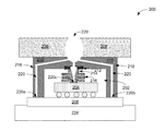
- FIG. 2 illustrates another embodiment of an apparatus 200 for moving devices under test to and from a testing socket of automatic test equipment in accordance with the present disclosure.
- the apparatus 200 includes a first heat conduction layer 208 , a second heat conduction layer 210 , a conformant layer 212 and a heat sink 214 .
- the heat sink 214 includes a plurality of fins 216 that are generally circular in shape.
- the second heat conduction layer 210 also includes legs 218 that are further in position away from the heat sink 214 as opposed to the legs 118 of the embodiment illustrated in FIG. 1 .
- the legs 218 can be part of the second heat conduction layer 210 , i.e. the legs 218 and the second heat conduction layer 210 can be a single entity, if desired.
- a vacuum path 220 is defined through the first and second heat conduction layers 208 , 210 , the conformant layer 212 and the heat sink 214 . Furthermore, the vacuum path 220 also extends through the legs 218 . Thus, the vacuum path 220 now terminates at three points 220 a , 220 b and 220 c for engaging the device under test 202 . Two of the three points, 220 a and 220 b defined within the legs 218 , can engage the substrate 206 of the device under test 202 . The third point, 220 c defined within the heat sink 214 , engages the semiconductor chip 204 of the device under test 202 .
- heat from the device under test 202 is conducted through the heat sink 214 and legs 218 to the second heat conduction layer 210 and thereby to the first heat conduction layer 208 .
- air is moved through the chamber of the automatic test equipment that includes the apparatus 200 and the socket 224 .
- the air moves through the fins 216 to thereby create a cooling effect of the heat sink 214 by extracting heat from the fins 216 .
- Such air movement helps move heat from the device under test 202 , and from around the device under test 202 , by extracting heat from the heat sink 214 .
- the heated air from the fins 216 can also help control the ambient temperature within the automatic test equipment chamber.
- heat can be conducted through the legs 218 to the second heat conduction layer 210 and thereby to the first heat conduction layer 208 .
- the conformant layer 212 provides adaptability for the apparatus 200 by allowing the apparatus 200 to be used with different sized devices for testing.
- the conformant layer 212 is generally a flexible or a “spring” type layer allowing the apparatus 200 to conform to various sized devices having different dimensions, such as, for example, height, thickness, etc., for testing when a vacuum is applied to cause the heat sink 214 to engage the device under test 202 and pull on the device under test 202 .
- the conformant layer 212 can also help protect the device under test 202 against cracking from too much pressure from apparatus 200 .
- the conformant layer 212 may be made from a heat conductive material to assist with conducting heat away from the device under test 202 or may be made from a heat resistant material.
- the first and second heat conduction layers 208 , 210 may be a single layer.
- the legs 218 may be a part of the second heat conduction layer 210 .
- the first and second heat conduction layers 208 , 210 and/or legs 218 may be a single entity.
- the first heat conduction layer 208 and second heat conduction layer 210 can be of various shapes such as, for example, circular, square, rectangular, etc.
- the first and second heat conduction layers 208 , 210 , heat sink 214 , as well as legs 218 can be made from various types of metal suitable for heat conduction
- FIG. 3 illustrates another embodiment of an apparatus 300 similar to the apparatus 200 illustrated in FIG. 2 .
- the apparatus 300 however does not include a conformant layer.
- the apparatus 300 illustrated in FIG. 3 does not include a vacuum path defined through the heat sink 314 to engage the semiconductor chip 304 of the device under test 302 .
- the apparatus 300 of FIG. 3 only includes two vacuum points 320 a , 320 b located within the legs 318 .
- the two vacuum points 320 a , 320 b in the apparatus of FIG. 3 engage a substrate of the device under test.
- the first and second heat conduction layers 308 , 310 may be a single layer.
- legs 318 may be a part of the second heat conduction layer 310 .
- the first and second heat conduction layers 308 , 310 and/or legs 318 may be a single entity.
- the first heat conduction layer 308 and second heat conduction layer 310 can be of various shapes such as, for example, circular, square, rectangular, etc.
- the first and second heat conduction layers 308 , 310 , heat sink 314 , as well as legs 318 can be made from various types of metal suitable for heat conduction.
- FIG. 4 illustrates another embodiment of an apparatus 400 for moving devices under test to and from a testing socket of automatic test equipment, in accordance with the present disclosure.
- the apparatus 400 illustrated in FIG. 4 includes a first heat conduction layer 408 , a second heat conduction layer 410 , and a heat sink 414 .
- the apparatus 400 is similar to the apparatus 300 illustrated in FIG. 3 but also includes a side heat conduction well defined by two legs 426 . The two legs 426 engage a docking plate 428 of the automatic test equipment.
- the air moving the chamber will move through the fins 416 of the heat sink 414 .
- heat will be conducted through the first and second heat conduction layers 408 , 410 . Additional heat will also be moved through the side heat conduction well as indicated by the arrows 430 .
- the first and second heat conduction layers 408 , 410 may be a single layer.
- legs 418 and/or legs 426 may be a part of the second heat conduction layer 410 .
- the first and second heat conduction layers 408 , 410 , legs 418 and/or legs 426 may be a single entity.
- the first heat conduction layer 408 and second heat conduction layer 410 can be of various shapes such as, for example, circular, square, rectangular, etc.
- the first and second heat conduction layers 408 , 410 , as well as legs 418 and 426 can be made from various types of metal suitable for heat conduction.
- FIG. 5 is a flow diagram of a method 500 of using an apparatus, such as one of the apparatuses illustrated in FIGS. 1-4 , to engage a micro-electronic device for testing in automatic test equipment.
- the apparatus generally comprises a heat sink, a heat conduction layer coupled to the heat sink, a first leg coupled to the heat conduction layer, a second leg coupled to the heat conduction layer, wherein the second leg is spaced apart from the first leg, wherein the heat sink comprises a plurality of fins extending from the heat sink, wherein the heat sink is configured to engage the device, and wherein a vacuum path is defined within the apparatus.
- the apparatus engages the device such that the heat sink engages the device.
- a vacuum is applied to the vacuum path to hold the device with the apparatus.
- air is moved within the automatic test equipment such that air moves past the fins.
- the present disclosure provides various apparatuses to allow for heat conduction around a device under test during testing of the device under test by automatic test equipment.
- the apparatuses are utilized to engage the device under test and move the device under test to and from a testing socket of the automatic test equipment. This is achieved by applying a vacuum source (not illustrated) to one of the apparatuses such that the termination points of the vacuum path defined within the apparatus engage the device under test and hold the device under test in place against the apparatus.
- a vacuum source not illustrated
- the apparatus also engages the device under test during testing.
- air movement within the testing chamber moves through fins included on the heat sink of the apparatuses. This helps extract heat from the heat sink into the air.
- heat is conducted through the heat sink to one or more heat conduction layers and/or legs depending upon the configuration of the apparatus. Accordingly, the apparatuses help control and maintain proper heating conditions for testing various micro-electronic devices such as semiconductor chips and devices. This can lead to improved testing of the micro-electronic devices and help prevent failure of devices under test due to overheating of the micro-electronic devices.
- One aspect can include an apparatus that is configured to engage a device for testing the device via automatic test equipment.
- the apparatus includes a heat sink, wherein the heat sink comprises a plurality of fins extending from the heat sink, and wherein the heat sink is configured to engage the device.
- the apparatus further includes a heat conduction layer coupled to the heat sink, a first leg coupled to the heat conduction layer, and a second leg coupled to the heat conduction layer. The second leg is spaced apart from the first leg.
- a vacuum path is defined through (i) the heat conduction layer and (ii) the heat sink. The vacuum path permits the apparatus to engage the device to be tested by the automatic test equipment.
- a conformant component can be coupled to the heat sink, wherein the conformant component is configured to adjust based upon dimensions of the device.
- the conformant component can comprise an o-ring.
- the vacuum path can be further defined through (i) the first leg and (ii) the second leg.
- the heat conduction layer can be a first heat conduction layer.
- the apparatus can further comprise a second heat conduction layer coupled to the first heat conduction layer and the vacuum path is further defined through the second heat conduction layer.
- the device can comprise a semiconductor chip coupled to a substrate.
- the first leg and the second leg can be configured to engage the substrate and the vacuum path can be defined through (i) the first leg and (ii) the second leg.
- the device can comprise a semiconductor chip and (i) the first leg and (ii) the second leg can be configured to engage the semiconductor chip.
- the heat conduction layer, the first leg and the second leg can be a single entity.
- the apparatus can further comprise a third leg coupled to the heat conduction layer and a fourth leg coupled to the heat conduction layer.
- the third leg and the fourth leg can be configured to engage a docking plate of the automatic test equipment.
- the heat conduction layer, the third leg and the fourth leg can be a single entity.
- the heat conduction layer, the first leg, the second leg, the third leg and the fourth leg can be a single entity.
- Another aspect can include a method of testing a device with automatic test equipment using an apparatus, wherein the apparatus comprises a heat sink, a heat conduction layer coupled to the heat sink, a first leg coupled to the heat conduction layer, a second leg coupled to the heat conduction layer, wherein the second leg is spaced apart from the first leg, wherein the heat sink comprises a plurality of fins extending from the heat sink, wherein the heat sink is configured to engage the device, and wherein a vacuum path is defined within the apparatus.
- the method comprises engaging the device with the apparatus such that the heat sink engages the device, applying a vacuum to the vacuum path to hold the device with the apparatus, and during testing of the device, moving air within the automatic test equipment such that air moves past the fins.
- the vacuum path can be defined through (i) the heat conduction layer, and (ii) the heat sink. Applying the vacuum to the vacuum path to hold the device with the apparatus can comprise applying the vacuum such that the apparatus holds the device against the heat sink.
- the device can comprise a semiconductor chip coupled to a substrate, and the first leg and the second leg are configured to engage the substrate.
- the phrase “A/B” means A or B.
- the phrase “A and/or B” means “(A), (B), or (A and B).”
- the phrase “at least one of A, B, and C” means “(A), (B), (C), (A and B), (A and C), (B and C), or (A, B and C).”
- the phrase “(A)B” means “(B) or (AB)” that is, A is an optional element.
Abstract
Description
Claims (18)
Priority Applications (4)
| Application Number | Priority Date | Filing Date | Title |
|---|---|---|---|
| US14/076,058 US9244107B2 (en) | 2012-11-12 | 2013-11-08 | Heat sink blade pack for device under test testing |
| PCT/US2013/069409 WO2014074977A2 (en) | 2012-11-12 | 2013-11-11 | Heat sink blade pack for device test testing |
| TW102140861A TWI603100B (en) | 2012-11-12 | 2013-11-11 | Heat sink blade pack for device under test testing |
| CN201380069846.4A CN104919325B (en) | 2012-11-12 | 2013-11-11 | Radiator leaf packet for device under test |
Applications Claiming Priority (2)
| Application Number | Priority Date | Filing Date | Title |
|---|---|---|---|
| US201261725241P | 2012-11-12 | 2012-11-12 | |
| US14/076,058 US9244107B2 (en) | 2012-11-12 | 2013-11-08 | Heat sink blade pack for device under test testing |
Publications (2)
| Publication Number | Publication Date |
|---|---|
| US20140132296A1 US20140132296A1 (en) | 2014-05-15 |
| US9244107B2 true US9244107B2 (en) | 2016-01-26 |
Family
ID=50681114
Family Applications (1)
| Application Number | Title | Priority Date | Filing Date |
|---|---|---|---|
| US14/076,058 Expired - Fee Related US9244107B2 (en) | 2012-11-12 | 2013-11-08 | Heat sink blade pack for device under test testing |
Country Status (4)
| Country | Link |
|---|---|
| US (1) | US9244107B2 (en) |
| CN (1) | CN104919325B (en) |
| TW (1) | TWI603100B (en) |
| WO (1) | WO2014074977A2 (en) |
Families Citing this family (1)
| Publication number | Priority date | Publication date | Assignee | Title |
|---|---|---|---|---|
| CN108037398B (en) * | 2018-01-16 | 2023-12-05 | 苏州精濑光电有限公司 | Aging test device and aging test method for display module |
Citations (28)
| Publication number | Priority date | Publication date | Assignee | Title |
|---|---|---|---|---|
| US6019166A (en) * | 1997-12-30 | 2000-02-01 | Intel Corporation | Pickup chuck with an integral heatsink |
| US6019164A (en) * | 1997-12-31 | 2000-02-01 | Temptronic Corporation | Workpiece chuck |
| US6073681A (en) * | 1997-12-31 | 2000-06-13 | Temptronic Corporation | Workpiece chuck |
| US6104203A (en) * | 1995-05-16 | 2000-08-15 | Trio-Tech International | Test apparatus for electronic components |
| US6119460A (en) * | 1998-05-25 | 2000-09-19 | Huang; Yun | Temperature control system for test heads |
| US6124725A (en) * | 1997-11-29 | 2000-09-26 | Tokyo Electron Limited | Apparatus and method for testing semiconductor devices formed on a semiconductor wafer |
| US6140616A (en) * | 1998-09-25 | 2000-10-31 | Aehr Test Systems | Wafer level burn-in and test thermal chuck and method |
| US6328096B1 (en) * | 1997-12-31 | 2001-12-11 | Temptronic Corporation | Workpiece chuck |
| US6415858B1 (en) * | 1997-12-31 | 2002-07-09 | Temptronic Corporation | Temperature control system for a workpiece chuck |
| US20020109518A1 (en) | 1998-11-25 | 2002-08-15 | Advantest Corporation | Device testing apparatus |
| US6501290B2 (en) * | 1999-09-29 | 2002-12-31 | Intel Corporation | Direct to chuck coolant delivery for integrated circuit testing |
| US20030030430A1 (en) * | 2001-08-10 | 2003-02-13 | Pfahnl Andreas C. | Methods and apparatus for testing a semiconductor structure using improved temperature desoak techniques |
| US6545494B1 (en) * | 2000-07-10 | 2003-04-08 | Temptronic Corporation | Apparatus and method for controlling temperature in a wafer using integrated temperature sensitive diode |
| US6552561B2 (en) * | 2000-07-10 | 2003-04-22 | Temptronic Corporation | Apparatus and method for controlling temperature in a device under test using integrated temperature sensitive diode |
| US6570374B1 (en) * | 2000-06-23 | 2003-05-27 | Honeywell International Inc. | Vacuum chuck with integrated electrical testing points |
| US6644703B1 (en) * | 1999-08-25 | 2003-11-11 | Core Flow Ltd. | Self-adaptive vacuum gripping system |
| US6700099B2 (en) * | 2000-07-10 | 2004-03-02 | Temptronic Corporation | Wafer chuck having thermal plate with interleaved heating and cooling elements, interchangeable top surface assemblies and hard coated layer surfaces |
| US6703853B1 (en) * | 2001-03-19 | 2004-03-09 | Advanced Micro Devices, Inc. | Test contact mechanism |
| US6886976B2 (en) * | 2001-04-10 | 2005-05-03 | Delta Design, Inc. | Method for controlling the temperature of an electronic component under test |
| US7501810B2 (en) * | 2000-09-05 | 2009-03-10 | Cascade Microtech, Inc. | Chuck for holding a device under test |
| US20090174427A1 (en) * | 2008-01-04 | 2009-07-09 | Texas Instruments Incorporated | Burn-in-board architecture and integrated circuit device transfer method |
| US7567090B2 (en) * | 2006-10-23 | 2009-07-28 | International Business Machines Corporation | Liquid recovery, collection method and apparatus in a non-recirculating test and burn-in application |
| US7852096B2 (en) * | 2004-05-18 | 2010-12-14 | Circuit Check | Spring-loaded, removable test fixture for circuit board testers |
| US20110095773A1 (en) * | 2009-10-26 | 2011-04-28 | Nec Corporation | cooling structure for a test device, and a method for testing a device |
| US20110267082A1 (en) * | 2010-04-30 | 2011-11-03 | International Business Machines Corporation | Methodologies and Test Configurations for Testing Thermal Interface Materials |
| US20110267084A1 (en) * | 2010-04-30 | 2011-11-03 | International Business Machines Corporation | Thermal interface material, test structure and method of use |
| US8268670B2 (en) * | 2003-10-07 | 2012-09-18 | Fujitsu Semiconductor Limited | Method of semiconductor device protection |
| US8468690B2 (en) * | 2007-11-26 | 2013-06-25 | Tokyo Electron Limited | Holding member for use in test and method for manufacturing same |
Family Cites Families (4)
| Publication number | Priority date | Publication date | Assignee | Title |
|---|---|---|---|---|
| KR20010024445A (en) * | 1997-10-07 | 2001-03-26 | 릴라이어빌리티 인코포레이티드 | Burn-in board capable of high power dissipation |
| IL135484A0 (en) * | 1997-10-07 | 2001-05-20 | Reliability Inc | Burn-in board with adaptable heat sink device |
| JP4906496B2 (en) * | 2006-12-25 | 2012-03-28 | 新光電気工業株式会社 | Semiconductor package |
| TWI405361B (en) * | 2008-12-31 | 2013-08-11 | Ind Tech Res Inst | Thermoelectric device and process thereof and stacked structure of chips and chip package structure |
-
2013
- 2013-11-08 US US14/076,058 patent/US9244107B2/en not_active Expired - Fee Related
- 2013-11-11 WO PCT/US2013/069409 patent/WO2014074977A2/en active Application Filing
- 2013-11-11 CN CN201380069846.4A patent/CN104919325B/en not_active Expired - Fee Related
- 2013-11-11 TW TW102140861A patent/TWI603100B/en not_active IP Right Cessation
Patent Citations (31)
| Publication number | Priority date | Publication date | Assignee | Title |
|---|---|---|---|---|
| US6104203A (en) * | 1995-05-16 | 2000-08-15 | Trio-Tech International | Test apparatus for electronic components |
| US6124725A (en) * | 1997-11-29 | 2000-09-26 | Tokyo Electron Limited | Apparatus and method for testing semiconductor devices formed on a semiconductor wafer |
| US6019166A (en) * | 1997-12-30 | 2000-02-01 | Intel Corporation | Pickup chuck with an integral heatsink |
| US6802368B2 (en) * | 1997-12-31 | 2004-10-12 | Temptronic Corporation | Temperature control system for a workpiece chuck |
| US6019164A (en) * | 1997-12-31 | 2000-02-01 | Temptronic Corporation | Workpiece chuck |
| US6073681A (en) * | 1997-12-31 | 2000-06-13 | Temptronic Corporation | Workpiece chuck |
| US6328096B1 (en) * | 1997-12-31 | 2001-12-11 | Temptronic Corporation | Workpiece chuck |
| US6415858B1 (en) * | 1997-12-31 | 2002-07-09 | Temptronic Corporation | Temperature control system for a workpiece chuck |
| US6540014B2 (en) * | 1997-12-31 | 2003-04-01 | Temptronic Corporation | Workpiece chuck |
| US6119460A (en) * | 1998-05-25 | 2000-09-19 | Huang; Yun | Temperature control system for test heads |
| US6140616A (en) * | 1998-09-25 | 2000-10-31 | Aehr Test Systems | Wafer level burn-in and test thermal chuck and method |
| US20020109518A1 (en) | 1998-11-25 | 2002-08-15 | Advantest Corporation | Device testing apparatus |
| US6644703B1 (en) * | 1999-08-25 | 2003-11-11 | Core Flow Ltd. | Self-adaptive vacuum gripping system |
| US6501290B2 (en) * | 1999-09-29 | 2002-12-31 | Intel Corporation | Direct to chuck coolant delivery for integrated circuit testing |
| US6570374B1 (en) * | 2000-06-23 | 2003-05-27 | Honeywell International Inc. | Vacuum chuck with integrated electrical testing points |
| US6552561B2 (en) * | 2000-07-10 | 2003-04-22 | Temptronic Corporation | Apparatus and method for controlling temperature in a device under test using integrated temperature sensitive diode |
| US6700099B2 (en) * | 2000-07-10 | 2004-03-02 | Temptronic Corporation | Wafer chuck having thermal plate with interleaved heating and cooling elements, interchangeable top surface assemblies and hard coated layer surfaces |
| US6545494B1 (en) * | 2000-07-10 | 2003-04-08 | Temptronic Corporation | Apparatus and method for controlling temperature in a wafer using integrated temperature sensitive diode |
| US7501810B2 (en) * | 2000-09-05 | 2009-03-10 | Cascade Microtech, Inc. | Chuck for holding a device under test |
| US6703853B1 (en) * | 2001-03-19 | 2004-03-09 | Advanced Micro Devices, Inc. | Test contact mechanism |
| US6886976B2 (en) * | 2001-04-10 | 2005-05-03 | Delta Design, Inc. | Method for controlling the temperature of an electronic component under test |
| US20030030430A1 (en) * | 2001-08-10 | 2003-02-13 | Pfahnl Andreas C. | Methods and apparatus for testing a semiconductor structure using improved temperature desoak techniques |
| US8268670B2 (en) * | 2003-10-07 | 2012-09-18 | Fujitsu Semiconductor Limited | Method of semiconductor device protection |
| US7852096B2 (en) * | 2004-05-18 | 2010-12-14 | Circuit Check | Spring-loaded, removable test fixture for circuit board testers |
| US7567090B2 (en) * | 2006-10-23 | 2009-07-28 | International Business Machines Corporation | Liquid recovery, collection method and apparatus in a non-recirculating test and burn-in application |
| US8468690B2 (en) * | 2007-11-26 | 2013-06-25 | Tokyo Electron Limited | Holding member for use in test and method for manufacturing same |
| US20090174427A1 (en) * | 2008-01-04 | 2009-07-09 | Texas Instruments Incorporated | Burn-in-board architecture and integrated circuit device transfer method |
| US20110095773A1 (en) * | 2009-10-26 | 2011-04-28 | Nec Corporation | cooling structure for a test device, and a method for testing a device |
| US20110267084A1 (en) * | 2010-04-30 | 2011-11-03 | International Business Machines Corporation | Thermal interface material, test structure and method of use |
| US20110267082A1 (en) * | 2010-04-30 | 2011-11-03 | International Business Machines Corporation | Methodologies and Test Configurations for Testing Thermal Interface Materials |
| US8471575B2 (en) * | 2010-04-30 | 2013-06-25 | International Business Machines Corporation | Methodologies and test configurations for testing thermal interface materials |
Also Published As
| Publication number | Publication date |
|---|---|
| CN104919325B (en) | 2017-10-10 |
| WO2014074977A2 (en) | 2014-05-15 |
| WO2014074977A3 (en) | 2014-07-17 |
| TWI603100B (en) | 2017-10-21 |
| TW201437654A (en) | 2014-10-01 |
| US20140132296A1 (en) | 2014-05-15 |
| CN104919325A (en) | 2015-09-16 |
Similar Documents
| Publication | Publication Date | Title |
|---|---|---|
| CN103367181B (en) | For the method and apparatus of bonded substrate | |
| Chao et al. | Low-temperature bonded GaN-on-diamond HEMTs with 11 W/mm output power at 10 GHz | |
| TWI518926B (en) | Chucks for supporting solar cell in hot spot testing | |
| US9377486B2 (en) | Thermal interface material handling for thermal control of an electronic component under test | |
| TWI436075B (en) | Semiconductor measuring device | |
| EP2434547A3 (en) | Gallium nitride based semiconductor devices and methods of manufacturing the same | |
| US9874596B2 (en) | Method for manufacturing silicon carbide semiconductor apparatus, and energization test apparatus | |
| EP2428996A3 (en) | Gallium Nitride Based Semiconductor Devices and Methods of Manufacturing the Same | |
| CN102347294A (en) | Semiconductor device | |
| EP3104417A3 (en) | Method of manufacturing a protective film for a solar cell | |
| EP3343594A3 (en) | Semiconductor device | |
| MY188301A (en) | Multi-chip self adjusting cooling solution | |
| US9244107B2 (en) | Heat sink blade pack for device under test testing | |
| JP2015165566A5 (en) | ||
| TWI633636B (en) | Electronic device and its manufacturing method | |
| WO2017111840A1 (en) | Conductive base embedded interconnect | |
| EP3273467A3 (en) | Semiconductor die backside devices and methods of fabrication thereof | |
| Palavesam et al. | Investigations of the fracture strength of thin silicon dies embedded in flexible foil substrates | |
| US9612274B2 (en) | Probe card and test apparatus including the same | |
| TWM452439U (en) | Low-temperature testing system for testing wafer-level integrated circuit | |
| JP2015154045A (en) | Semiconductor device manufacturing method | |
| US20180235069A1 (en) | Pressure limiting heat sink | |
| CN105728995B (en) | A kind of parallel seam sealing machine closure holder | |
| US20210327745A1 (en) | Pickup and contact device | |
| Endoh et al. | Heat dissipation characterization and application of SiC power devices by transient thermal measurement |
Legal Events
| Date | Code | Title | Description |
|---|---|---|---|
| AS | Assignment |
Owner name: MARVELL SEMICONDUCTOR, INC., CALIFORNIA Free format text: ASSIGNMENT OF ASSIGNORS INTEREST;ASSIGNORS:TIRADO, BRUCE;WU, SCOTT;SU, WILLIAM;AND OTHERS;SIGNING DATES FROM 20131108 TO 20151108;REEL/FRAME:036996/0573 Owner name: MARVELL INTERNATIONAL LTD., BERMUDA Free format text: ASSIGNMENT OF ASSIGNORS INTEREST;ASSIGNOR:MARVELL SEMICONDUCTOR, INC.;REEL/FRAME:036996/0725 Effective date: 20140818 Owner name: MARVELL WORLD TRADE LTD., BARBADOS Free format text: ASSIGNMENT OF ASSIGNORS INTEREST;ASSIGNOR:MARVELL INTERNATIONAL LTD.;REEL/FRAME:036996/0737 Effective date: 20150828 |
|
| AS | Assignment |
Owner name: MARVELL INTERNATIONAL LTD., BERMUDA Free format text: LICENSE;ASSIGNOR:MARVELL WORLD TRADE LTD.;REEL/FRAME:037182/0779 Effective date: 20150929 |
|
| STCF | Information on status: patent grant |
Free format text: PATENTED CASE |
|
| FEPP | Fee payment procedure |
Free format text: MAINTENANCE FEE REMINDER MAILED (ORIGINAL EVENT CODE: REM.); ENTITY STATUS OF PATENT OWNER: LARGE ENTITY |
|
| AS | Assignment |
Owner name: MARVELL INTERNATIONAL LTD., BERMUDA Free format text: ASSIGNMENT OF ASSIGNORS INTEREST;ASSIGNOR:MARVELL WORLD TRADE LTD.;REEL/FRAME:051778/0537 Effective date: 20191231 |
|
| AS | Assignment |
Owner name: CAVIUM INTERNATIONAL, CAYMAN ISLANDS Free format text: ASSIGNMENT OF ASSIGNORS INTEREST;ASSIGNOR:MARVELL INTERNATIONAL LTD.;REEL/FRAME:052918/0001 Effective date: 20191231 |
|
| LAPS | Lapse for failure to pay maintenance fees |
Free format text: PATENT EXPIRED FOR FAILURE TO PAY MAINTENANCE FEES (ORIGINAL EVENT CODE: EXP.); ENTITY STATUS OF PATENT OWNER: LARGE ENTITY |
|
| STCH | Information on status: patent discontinuation |
Free format text: PATENT EXPIRED DUE TO NONPAYMENT OF MAINTENANCE FEES UNDER 37 CFR 1.362 |
|
| FP | Lapsed due to failure to pay maintenance fee |
Effective date: 20200126 |
|
| AS | Assignment |
Owner name: MARVELL ASIA PTE, LTD., SINGAPORE Free format text: ASSIGNMENT OF ASSIGNORS INTEREST;ASSIGNOR:CAVIUM INTERNATIONAL;REEL/FRAME:053475/0001 Effective date: 20191231 |