US9245790B2 - Integrated circuits and methods of forming the same with multiple embedded interconnect connection to same through-semiconductor via - Google Patents
Integrated circuits and methods of forming the same with multiple embedded interconnect connection to same through-semiconductor via Download PDFInfo
- Publication number
- US9245790B2 US9245790B2 US13/747,579 US201313747579A US9245790B2 US 9245790 B2 US9245790 B2 US 9245790B2 US 201313747579 A US201313747579 A US 201313747579A US 9245790 B2 US9245790 B2 US 9245790B2
- Authority
- US
- United States
- Prior art keywords
- semiconductor
- interconnect
- vias
- dielectric layer
- interlayer dielectric
- Prior art date
- Legal status (The legal status is an assumption and is not a legal conclusion. Google has not performed a legal analysis and makes no representation as to the accuracy of the status listed.)
- Active, expires
Links
Images


Classifications
-
- H—ELECTRICITY
- H01—ELECTRIC ELEMENTS
- H01L—SEMICONDUCTOR DEVICES NOT COVERED BY CLASS H10
- H01L21/00—Processes or apparatus adapted for the manufacture or treatment of semiconductor or solid state devices or of parts thereof
- H01L21/70—Manufacture or treatment of devices consisting of a plurality of solid state components formed in or on a common substrate or of parts thereof; Manufacture of integrated circuit devices or of parts thereof
- H01L21/71—Manufacture of specific parts of devices defined in group H01L21/70
- H01L21/768—Applying interconnections to be used for carrying current between separate components within a device comprising conductors and dielectrics
- H01L21/76801—Applying interconnections to be used for carrying current between separate components within a device comprising conductors and dielectrics characterised by the formation and the after-treatment of the dielectrics, e.g. smoothing
- H01L21/76802—Applying interconnections to be used for carrying current between separate components within a device comprising conductors and dielectrics characterised by the formation and the after-treatment of the dielectrics, e.g. smoothing by forming openings in dielectrics
- H01L21/76807—Applying interconnections to be used for carrying current between separate components within a device comprising conductors and dielectrics characterised by the formation and the after-treatment of the dielectrics, e.g. smoothing by forming openings in dielectrics for dual damascene structures
-
- H—ELECTRICITY
- H01—ELECTRIC ELEMENTS
- H01L—SEMICONDUCTOR DEVICES NOT COVERED BY CLASS H10
- H01L21/00—Processes or apparatus adapted for the manufacture or treatment of semiconductor or solid state devices or of parts thereof
- H01L21/70—Manufacture or treatment of devices consisting of a plurality of solid state components formed in or on a common substrate or of parts thereof; Manufacture of integrated circuit devices or of parts thereof
- H01L21/71—Manufacture of specific parts of devices defined in group H01L21/70
- H01L21/768—Applying interconnections to be used for carrying current between separate components within a device comprising conductors and dielectrics
- H01L21/76898—Applying interconnections to be used for carrying current between separate components within a device comprising conductors and dielectrics formed through a semiconductor substrate
-
- H—ELECTRICITY
- H01—ELECTRIC ELEMENTS
- H01L—SEMICONDUCTOR DEVICES NOT COVERED BY CLASS H10
- H01L23/00—Details of semiconductor or other solid state devices
- H01L23/52—Arrangements for conducting electric current within the device in operation from one component to another, i.e. interconnections, e.g. wires, lead frames
- H01L23/522—Arrangements for conducting electric current within the device in operation from one component to another, i.e. interconnections, e.g. wires, lead frames including external interconnections consisting of a multilayer structure of conductive and insulating layers inseparably formed on the semiconductor body
- H01L23/528—Geometry or layout of the interconnection structure
- H01L23/5286—Arrangements of power or ground buses
-
- H—ELECTRICITY
- H01—ELECTRIC ELEMENTS
- H01L—SEMICONDUCTOR DEVICES NOT COVERED BY CLASS H10
- H01L2924/00—Indexing scheme for arrangements or methods for connecting or disconnecting semiconductor or solid-state bodies as covered by H01L24/00
-
- H—ELECTRICITY
- H01—ELECTRIC ELEMENTS
- H01L—SEMICONDUCTOR DEVICES NOT COVERED BY CLASS H10
- H01L2924/00—Indexing scheme for arrangements or methods for connecting or disconnecting semiconductor or solid-state bodies as covered by H01L24/00
- H01L2924/0001—Technical content checked by a classifier
- H01L2924/0002—Not covered by any one of groups H01L24/00, H01L24/00 and H01L2224/00
Definitions
- the present invention generally relates to integrated circuits and methods of forming integrated circuits, and more particularly relates to integrated circuits and methods of forming integrated circuits with embedded interconnect vias disposed in an interlayer dielectric layer and in electrical communication to a through-semiconductor via.
- a plurality of semiconductor devices e.g., transistors, resistors, and the like
- the semiconductor devices are connected by a network of electrically-conductive lines, vias, and interconnect structures.
- the network of electrically-conductive lines, vias, and interconnect structures selectively connect the semiconductor devices to each other and to various other devices such as, but not limited to, a power source, clocks, signals, addresses, and input and output sources, and also connect the semiconductor devices to subsequently-formed semiconductor devices.
- ICs integrated circuits
- electrically-conductive vias are integrally formed within the semiconductor substrate and extend across various levels of integrated circuits to provide power to the different levels.
- Such electrically-conductive vias are known in the art as through-semiconductor vias.
- the through-semiconductor vias are formed during the BEOL semiconductor fabrication process by selectively etching a recess through any dielectric layers that overlie the semiconductor substrate and at least partially into the semiconductor substrate, followed by depositing metal such as copper in the recess and chemical-mechanical planarization (CMP) to remove excess metal from outside of the recess. Subsequent layers are then formed over the dielectric layers and the through-semiconductor via, including a metal layer that selectively connects the through-semiconductor vias to a power source and to the semiconductor devices.
- CMP chemical-mechanical planarization
- Void formation is a common problem associated with forming subsequent layers over the through-semiconductor via. Without being bound to any particular theory, it is believed that void formation is attributable to migration of metal ions from the through-semiconductor vias into the interface between the through-semiconductor vias and the metal layer or dielectric layers that overlie the through-semiconductor vias. It is believed that the migration of the metal ions causes stress-induced warping in the subsequent layers, thereby creating voids between the through-semiconductor vias and the metal layer that overlies the through-semiconductor vias.
- connections between the through-semiconductor vias and the subsequent layers may be compromised at various locations, resulting in loss of electrical communication between the through-semiconductor vias and the subsequent metal layer that overlies the through-semiconductor vias.
- Subsequent layers that overlie the through-semiconductor vias generally include metal lines that extend over a surface of the through-semiconductor via and a number of conductive layers that are electrically connected to the through-semiconductor vias and the metal lines. Successful connection between the metal lines and the through-semiconductor via can be sensed based upon whether electrical current flows between the metal lines and the through-semiconductor via.
- connection fails to provide a useful mechanism for sensing void formation because the electrical current will still flow between the metal lines and the through-semiconductor vias so long as a void does not completely block a connection between the metal lines and the through-semiconductor vias, and the presence of the void may cause premature device failure.
- a method of forming an integrated circuit includes forming a plurality of semiconductor devices on a semiconductor substrate.
- a through-semiconductor via is formed in the semiconductor substrate, and an interlayer dielectric layer is formed that overlies the through-semiconductor via and the plurality of semiconductor devices.
- a first interconnect via is embedded within the interlayer dielectric layer, and a second interconnect via is embedded within the interlayer dielectric layer. The first interconnect via and the second interconnect via are in electrical communication with the through-semiconductor via at spaced locations from each other on the through-semiconductor via.
- a method of sensing voiding between a through-semiconductor via and a subsequent layer that overlies the through-semiconductor via in an integrated circuit includes providing the integrated circuit that includes a plurality of semiconductor devices disposed on a semiconductor substrate.
- a through-semiconductor via is disposed in the semiconductor substrate of the integrated circuit, and an interlayer dielectric layer overlies the through-semiconductor via and the plurality of semiconductor devices.
- a first interconnect via is embedded within the interlayer dielectric layer, and a second interconnect via is embedded within the interlayer dielectric layer.
- the first interconnect via and the second interconnect via are in electrical communication with the through-semiconductor vias at spaced locations from each other on the through-semiconductor via to form an electrical connection.
- An electrical current is passed through the electrical connection between the first interconnect via and the second interconnect via, through the through-semiconductor via. Electrical resistance to passage of the electrical current in the electrical connection is measured between the first interconnect via and the second interconnect via to enable voiding to be sensed.
- an integrated circuit in another embodiment, includes a semiconductor substrate and a plurality of semiconductor devices disposed on the semiconductor substrate.
- a through-semiconductor via is disposed in the semiconductor substrate and an interlayer dielectric layer overlies the through-semiconductor via and the plurality of semiconductor devices.
- a first interconnect via is embedded within the interlayer dielectric layer, and a second interconnect via is embedded within the interlayer dielectric layer. The first interconnect via and the second interconnect via are in electrical communication with the through-semiconductor vias at spaced locations from each other on the through-semiconductor via.
- FIG. 1 is a schematic cross-sectional side view of a portion of an integrated circuit including a semiconductor substrate and transistors formed on the semiconductor substrate, with via holes for through-semiconductor vias formed in the integrated circuit;
- FIG. 2 is a schematic cross-sectional side view of the portion of the integrated circuit as shown in FIG. 1 , with through-semiconductor vias formed in the via holes;
- FIG. 3 is a schematic cross-sectional side view of the portion of the integrated circuit as shown in FIG. 2 , with an interlayer dielectric layer formed that overlies the through-semiconductor vias and the transistors, illustrating printing of a resist film over the interlayer dielectric layer;
- FIG. 4 is a schematic cross-sectional side view of the portion of the integrated circuit as shown in FIG. 3 , illustrating etching of the interlayer dielectric layer to form a pattern in the interlayer dielectric layer through gaps in the resist film;
- FIG. 5 is a schematic cross-sectional side view of the portion of the integrated circuit as shown in FIG. 4 after filling the pattern and interconnect holes with electrically-conductive material to form a first metal layer and interconnect vias, respectively;
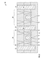
- FIG. 6 is an expanded schematic top view of another embodiment of an integrated circuit after filling the pattern and the interconnect holes with electrically-conductive material to form a first metal layer and interconnect vias, respectively.
- the integrated circuits include a semiconductor substrate having a plurality of semiconductor devices formed thereon, with a through-semiconductor via formed in the semiconductor substrate for supplying electricity through various layers of the integrated circuit.
- An interlayer dielectric layer is formed that overlies the through-semiconductor via and the plurality of semiconductor devices.
- a first interconnect via is embedded within the interlayer dielectric layer
- a second interconnect via is embedded within the interlayer dielectric layer with the first interconnect via and the second interconnect via in electrical communication with the through-semiconductor vias.
- the first interconnect via and the second interconnect via are embedded in the interlayer dielectric layer at spaced locations from each other on the through-semiconductor via.
- electrical connection to the through-semiconductor via with a single metal line is prone to void formation between the single metal line and the through-semiconductor via, whereas the first interconnect via and the second interconnect via each have a lesser contact area than traditional electrical connections to the through-semiconductor via with a single metal line.
- impact of void formation can be minimized while maintaining substantially uniform electrical contact between the first interconnect via and the second interconnect via across the through-semiconductor via.
- voiding between through-semiconductor via and a subsequent layer that overlies the through-semiconductor via can be measured by passing electrical current between the first interconnect via and the second interconnect via, through the through-semiconductor via, and by measuring resistivity.
- FIGS. 1-5 an embodiment of an integrated circuit 10 and a method of forming the integrated circuit 10 will now be described, with FIG. 5 showing the integrated circuit 10 that is formed in accordance with the method as shown sequentially in FIGS. 1-4 .
- a plurality of semiconductor devices 12 are formed on a semiconductor substrate 14 , and the semiconductor devices 12 are present in the resulting integrated circuit 10 as shown in FIG. 5 .
- the semiconductor substrate 14 includes semiconductor material such as any group IV semiconductor material.
- suitable semiconductor materials include, but are not limited to, those chosen from silicon, silicon germanium (SiGe), germanium (Ge), gallium arsenide (GaAs), or indium phosphide (InP).
- the semiconductor material is a silicon-containing material, such as mono- or poly-crystalline silicon, and the semiconductor substrate 14 may contain one or more doped regions 16 of the silicon-containing material.
- the semiconductor substrate 14 is shown as a base substrate with no further structure beneath the semiconductor substrate 14 ; however, although not shown, it is to be appreciated that the semiconductor substrate 14 can be an intermediate substrate within a stack of alternating layers produced through front-end-of-line (FEOL) fabrication and back-end-of-line (BEOL) fabrication techniques to form the integrated circuit 10 .
- the semiconductor devices 12 include, but are not limited to, transistors, capacitors, resistors, or the like.
- the semiconductor devices 12 are transistors that include a gate electrode 18 with embedded electrical contacts 20 that provide electrical connections on opposite sides of the gate electrode 18 .
- a dielectric layer 28 is formed that overlies the semiconductor substrate 14 , gate electrode 18 , and the embedded electrical contacts 20 are formed in the dielectric layer 28 through techniques known in the art.
- a through-semiconductor via 22 is formed in the semiconductor substrate 14 , with the through-semiconductor via 22 disposed in the semiconductor substrate 14 of the resulting integrated circuit 10 as shown in FIG. 5 .
- a plurality of the through-semiconductor vias 22 is formed in the semiconductor substrate 14 with the semiconductor substrate 14 surrounding the through-semiconductor vias 22 , with regions 24 of the semiconductor substrate 14 that are adjacent to the through-semiconductor vias 22 having at least one semiconductor device 12 formed thereon.
- the through-semiconductor vias 22 at least partially extend into the semiconductor substrate 14 , and generally extend completely through the semiconductor substrate 14 , to clearly define the regions 24 of the semiconductor substrate 14 that are adjacent to the through-semiconductor vias 22 .
- “through-semiconductor”, as the phase is used herein, does not necessarily require that the through-semiconductor via 22 extends completely through the semiconductor substrate 14 .
- the through-semiconductor via 22 includes an electrically-conductive material such as, but not limited to, metals including copper, tungsten, aluminum, silver, gold, other metals, or alloys thereof.
- the through-semiconductor via 22 enables semiconductor devices 12 in different levels of the integrated circuit 10 to be connected to a power source (not shown) and to other devices within the integrated circuit 10 , with the through-semiconductor via 22 embedded directly within the integrated circuit 10 to provide a common line that passes through various layers of the integrated circuit 10 .
- the through-semiconductor via 22 enables the integrated circuits 10 to be scaled down without sacrificing robust electrical connections between the semiconductor devices 12 and the power source, and further provides manufacturing efficiencies by avoiding the need for separate wiring schemes to be implemented after forming the integrated circuits 10 .
- the through-semiconductor via 22 is formed by etching a via hole 23 into the semiconductor substrate 14 , including through any dielectric layers 28 that overlie the semiconductor devices 12 , to form the regions 24 of the semiconductor substrate 14 on either side of the via hole 23 .
- a protecting layer 26 of dielectric material is formed over dielectric layers 28 that overlie the semiconductor devices 12 , with the protecting layer 26 including dielectric material that has a materially different etch rate in particular etchants than the dielectric layer 28 that is immediately beneath the protecting layer 26 .
- an etchant and etching technique that is effective to etch one of the layers etches another of the layers at a rate that is measurably slower, such as at least 50 percent slower.
- the protecting layer 26 thus functions as a hard mask, whereby the protecting layer 26 is patterned with the pattern in the protecting layer 26 transferred to underlying dielectric layers 28 .
- known techniques can be employed that utilize printing to pattern a resist film (not shown) over the protecting layer 26 , with the resist film patterned with a desired configuration of the via hole 23 , followed by etching the protecting layer 26 through the pattern in the resist film with an appropriate etchant that preferentially etches the protecting layer 26 to transfer the pattern in the resist film into the protecting layer 26 .
- the protecting layer 26 includes a nitrogen-containing silicon material such as nitrogen-doped silicon carbide or Si—N—C—H (NBLoK), and the dielectric layer 28 that is immediately beneath the protecting layer 26 includes an oxide such as silicon dioxide, with known etchants employed for etching that preferentially etch the nitrogen-containing silicon material and the oxide.
- Suitable etchants for nitrogen-containing silicon material include, but are not limited to, CHF 3 /O 2 mixtures, and etching of the protecting layer 26 can be conducted through dry etching techniques.
- suitable oxide etchants include, but are not limited to, CHF 3 , CF 4 , or SF 6 .
- the oxide may be etched through dry etching techniques, also referred to in the art as plasma etching techniques.
- the semiconductor substrate 14 may then be etched to form the at least one via hole 23 through known etching techniques, such as isotropic etching using SF6 and C4F8.
- etching techniques such as isotropic etching using SF6 and C4F8.
- the term “dielectric layer” encompasses one or more individual dielectric layers that overlie the semiconductor devices 12 .
- the dielectric layer 28 may include a single layer (not shown).
- more than two individual layers can be present in the dielectric layer 28 in other embodiments, depending upon particular architecture of the semiconductor devices 12 and electrical connections to the semiconductor devices 12 .
- the through-semiconductor via 22 is formed in the via hole in the semiconductor substrate 14 , such as through deposition of electrically-conductive material in the via hole while the protecting layer is still in place followed by chemical-mechanical planarization (CMP) of the protecting layer and excess electrically-conductive material that is outside of the via hole.
- CMP chemical-mechanical planarization
- an interlayer dielectric layer 30 is formed that overlies the through-semiconductor via 22 and the plurality of semiconductor devices 12 . More particularly, the interlayer dielectric layer 30 is formed overlying the through-semiconductor via 22 and any dielectric layers 28 that overlie the semiconductor devices 12 and that remain after forming the through-semiconductor via 22 (i.e., dielectric layers 28 that are formed during the FEOL fabrication).
- the “interlayer dielectric layer” refers to a layer or layers of dielectric material that are formed during BEOL fabrication and that at least partially remain in the integrated circuit 10 after fabrication.
- the interlayer dielectric layer 30 can include only a single layer (not shown).
- the interlayer dielectric layer 30 includes a combination of separate layers 31 , 32 , 33 that include different dielectric materials that have materially different etch rates in different etchants for purposes of selectively etching the interlayer dielectric layer 30 in the same manner as described above in the context of forming the through-semiconductor via 22 .
- additional layers of dielectric material may be formed that are subsequently completely removed during fabrication, such as a hard mask 34 that is described in further detail below, and such additional layers are not encompassed by the “interlayer dielectric layer” as referred to herein if such layers are ultimately removed from the integrated circuit 10 .
- additional layers may also be present in layer 30 , including dielectric layers and/or metal layers, and the structure shown in the Figures for the interlayer dielectric layer is not limited to only the layers 31 , 32 , 33 that are explicitly shown.
- a pattern is formed in the interlayer dielectric layer 30 in the same manner as described above for forming the through-semiconductor via 22 , where the protecting layer is employed and is patterned using printing of a resist film.
- a resist film 40 is formed over the interlayer dielectric layer 30 and patterned through printing.
- a pattern in the resist film 40 is transferred to a hard mask 34 , which is comparable to the protecting layer as described above. As shown in FIG.
- a pattern 36 is then etched in the interlayer dielectric layer 30 over the through-semiconductor via 22 or the plurality of the through-semiconductor vias 22 , through the pattern 36 in the hard mask 34 , to transfer the pattern 36 into the interlayer dielectric layer 30 .
- Portions of the hard mask 34 that remain after etching are generally shown in FIG. 4 .
- material of the hard mask 34 is substantially resistant to etchants that are effective for etching the interlayer dielectric layer 30 , or an individual layer 31 thereof that is immediately beneath the hard mask 34 , and the hard mask 34 is not completely removed during etching of the interlayer dielectric layer 30 such that the hard mask 34 is effective for maintaining the shape of the pattern 36 during etching of the interlayer dielectric layer 30 .
- the hard mask 34 includes metal, although it is to be appreciated that other known materials for hard masks can also be used and the hard masks described herein are not limited to any particular material. However, it is to be appreciated that suitable integration schemes are not limited to the preceding examples.
- the interlayer dielectric layer 30 may include separate layers 31 , 32 , 33 including different materials that have different etch rates in different etchants, and selection of particular materials can be employed to control etching of the interlayer dielectric layer 30 .
- one of the separate layers 31 , 32 , 33 included in the interlayer dielectric layer 30 is an etch stop layer 32 , which may be employed to isolate etching of the pattern 36 to a particular depth within the interlayer dielectric layer 30 .
- the etch stop layer 32 includes a material, such as a nitrogen-containing silicon material, and the etch stop layer 32 is spaced from the hard mask 34 by another separate layer 31 in the interlayer dielectric layer 30 that has a materially different etch rate in nitride etchants than the etch stop layer 32 , such as an oxide.
- the etch stop layer 32 may be thinner than the hard mask 34 to enable eventual etching through the etch stop layer 32 without completely removing the hard mask 34 .
- Etching the interlayer dielectric layer 30 through the pattern 36 in the hard mask 34 may be conducted in the same manner as described above in the context of FIG.
- a first interconnect via 42 and a second interconnect via 43 are embedded within the interlayer dielectric layer 30 to establish an electrical connection to the through-semiconductor via 22 , as shown in FIG. 5 .
- a first interconnect hole 44 and a second interconnect hole 45 are etched through the interlayer dielectric layer 30 in the pattern 36 to expose a surface 46 of the through-semiconductor via 22 in the first interconnect hole 44 and the second interconnect hole 45 .
- the first interconnect hole 44 and the second interconnect hole 45 are formed by patterning the etch stop layer 32 in portions of the etch stop layer 32 that are exposed in the pattern 36 and that overlie the through-semiconductor via 22 , followed by etching through any remaining separate layers 33 of the interlayer dielectric layer 30 that are beneath the etch stop layer 32 to expose the surface 46 of the through-semiconductor via 22 .
- gaps in a configuration of the first interconnect hole 44 and the second interconnect hole 45 may be pre-patterned in the etch stop layer 32 prior to forming subsequent separate layers 31 of the interlayer dielectric layer 30 over the etch stop layer 32 .
- etching may propagate through the gaps in the etch stop layer 32 that are exposed in the pattern 36 to effectively provide for interconnect hole formation concurrently with etching of the pattern 36 in the interlayer dielectric layer 30 .
- suitable integration schemes are not limited to the preceding examples.
- the first interconnect via 42 and the second interconnect via 43 are in electrical communication with one of the through-semiconductor via 22 at spaced locations from each other on the through-semiconductor via 22 .
- the first interconnect via 42 and the second interconnect via 43 are embedded within the interlayer dielectric layer 30 for each of the through-semiconductor vias 22 .
- Dielectric material of the interlayer dielectric layer 30 separates the first interconnect via 42 from the second interconnect via 43 from direct physical contact.
- an electrical connection between the first interconnect via 42 and the through-semiconductor via 22 can be established separate from an electrical connection between the second interconnect via 43 and the same through-semiconductor via 22 , as shown in FIG. 5 , which provides for numerous benefits including an ability to test for voiding between the through-semiconductor via 22 and either the interconnect vias 42 , 43 or the interlayer dielectric layer 30 , as described in further detail below.
- the first interconnect via 42 and the second interconnect via 43 by providing the first interconnect via 42 and the second interconnect via 43 , less contact area between the interconnect vias 42 , 43 and the through-semiconductor via 22 exists, which minimizes the incidence and impact of potential void formation on the respective electrical connections between the interconnect vias 42 , 43 and the through-semiconductor via 22 .
- a plurality of first interconnect vias 42 and a plurality of second interconnect vias 43 are embedded within the interlayer dielectric layer 30 with dielectric material of the interlayer dielectric layer 30 separating each interconnect via 42 , 43 from direct physical contact with each other.
- the plurality of first interconnect vias 42 is in electrical communication with one of the plurality of through-semiconductor vias 22 , i.e., each through-semiconductor via 22 may have a plurality of first interconnect vias 42 associated therewith.
- the plurality of second interconnect vias 43 is in electrical communication with one of the plurality of through-semiconductor vias 22 , such as the same through-semiconductor via 22 with which the plurality of first interconnect vias 42 is in electrical communication.
- the plurality of first interconnect vias 42 and the plurality of second interconnect vias 43 are embedded in different configurations over different through-semiconductor vias 22 , which enables different possible locations of voids to be detected and/or marginalized over different through-semiconductor vias 22 .
- a first electrically-conductive line 48 is formed that overlies and is in electrical communication with the first interconnect via 42 .
- the first electrically-conductive line 48 is separated from direct physical contact with the second interconnect via 43 by dielectric material of the interlayer dielectric layer 30 so that the first electrically-conductive line 48 is only in physical contact with the first interconnect via 42 .
- a second electrically-conductive line 49 is also formed overlying and in electrical communication with the second interconnect via 43 , with the second electrically-conductive line 49 separated from direct physical contact with the first interconnect via 42 by dielectric material of the interlayer dielectric layer 30 .
- an electrical circuit is formed between the first electrically-conductive line 48 and the second electrically-conductive line 49 , through the first interconnect via 42 , the through-semiconductor via 22 , and the second interconnect via 43 .
- an array 50 of first electrically-conductive lines 48 and second electrically-conductive lines 49 are formed.
- the first electrically-conductive lines 48 overlie and are in electrical communication with the plurality of first interconnect vias 42 that is associated with adjacent through-semiconductor vias 22
- the second electrically-conductive lines 49 overlie and are in electrical communication with the plurality of second interconnect vias 43 that is associated with adjacent through-semiconductor vias 22
- a plurality of through-semiconductor vias 22 in electrical communication through the array 50 of first electrically-conductive lines 48 and second electrically-conductive lines 49 .
- an electrical end terminal 52 is formed that is associated with end electrically-conductive lines at ends of the array 50 , with FIG. 6 showing two electrical end terminals 52 formed at ends of the array 50 .
- an electrical internal terminal 54 may be formed that is associated with internal electrically-conductive lines that are internal within the array 50 . In this manner, specific through-semiconductor vias 22 can be isolated for either testing or operation by supplying electricity through the electrical end terminals 52 or electrical internal terminals 54 .
- first electrically-conductive line 48 and the second electrically-conductive line 49 a metal-containing material is deposited in the pattern 36 .
- the first electrically-conductive line 48 and the second electrically-conductive line 49 are the layers formed after filling the pattern 36 with the metal-containing material, as distinguished from the interconnect vias 42 , 43 that establish electrical communication between the through-semiconductor via 22 and the electrically-conductive lines 48 , 49 .
- the metal-containing material includes, but is not limited to, metals such as copper, tungsten, aluminum, silver, gold, or alloys thereof, and it is to be appreciated that components other than metals may be present in the metal-containing material provided that the first electrically-conductive line 48 and the second electrically-conductive line 49 are capable conducting electricity.
- the first interconnect via 42 and the second interconnect via 43 are embedded in the interlayer dielectric layer 30 by concurrently filling the interconnect holes along with depositing the metal-containing material in the pattern 36 .
- first interconnect via 42 and/or the second interconnect via 43 may be formed prior to forming the first electrically-conductive line 48 and the second electrically-conductive line 49 .
- additional interlayer dielectric layers and additional metal layers may be formed over the first electrically-conductive line 48 and the second electrically-conductive line 49 in accordance with known fabrication techniques for integrated circuits. It is also to be appreciated that additional structure may be present below the semiconductor substrate 14 shown in FIGS. 1-5 , although no such additional structures are shown. Furthermore, numerous repeating structures as shown in FIGS. 1-5 can be stacked in the integrated circuit 10 to establish electrical connections through the through-semiconductor vias 22 .
- the features of the integrated circuits 10 described herein enable testing to be conducted for voiding between the through-semiconductor via 22 and either the interconnect vias 42 , 43 or interlayer dielectric layer 30 .
- a method of sensing voiding between the through-semiconductor via and a subsequent layer that overlies the through-semiconductor via in the integrated circuit 10 is provided.
- an integrated circuit 10 is provided as described above.
- An electrical current is passed through the electrical connection between the first interconnect via 42 and the second interconnect via 43 , through the through-semiconductor via 22 .
- the electrical current is passed through the electrical connections between the first interconnect via 42 and the second interconnect via 43 , through the through-semiconductor vias 22 , for a plurality of through-semiconductor vias 22 in series, such as when the array 50 of first electrically-conductive lines 48 and second electrically-conductive lines 49 are formed.
- electrical current can be passed through the first interconnect via 42 and the second interconnect via 43 that are associated with a single through-semiconductor via 22 .
- Electrical resistance to passage of the electrical current is then measured in the electrical connection between the first interconnect via 42 and the second interconnect via 43 , with the measurements associated with single through-semiconductor vias 22 or sections of through-semiconductor vias 22 depending upon which electrical end terminals 52 or electrical internal terminals 54 are used.
- electrical resistance may be measured in electrical connections between the electrically-conductive lines 48 , 49 , through the through-semiconductor vias 22 , at a plurality of locations in the array 50 . Based upon the measurements of electrical resistance, determinations can be made as to whether the first interconnect via 42 and the second interconnect via 43 provide an acceptable electrical connection with the corresponding through-semiconductor via 22 .
- the measured electrical resistance is compared to a benchmark electrical resistance value for the electrical connection between the first interconnect via 42 and the second interconnect via 43 , through the through-semiconductor via 22 . Based upon such comparison, determinations can be made as to whether the integrated circuits 10 are acceptable or whether modifications to fabrication of the integrated circuits 10 , 610 are necessary.
Abstract
Description
Claims (8)
Priority Applications (1)
| Application Number | Priority Date | Filing Date | Title |
|---|---|---|---|
| US13/747,579 US9245790B2 (en) | 2013-01-23 | 2013-01-23 | Integrated circuits and methods of forming the same with multiple embedded interconnect connection to same through-semiconductor via |
Applications Claiming Priority (1)
| Application Number | Priority Date | Filing Date | Title |
|---|---|---|---|
| US13/747,579 US9245790B2 (en) | 2013-01-23 | 2013-01-23 | Integrated circuits and methods of forming the same with multiple embedded interconnect connection to same through-semiconductor via |
Publications (2)
| Publication Number | Publication Date |
|---|---|
| US20140203827A1 US20140203827A1 (en) | 2014-07-24 |
| US9245790B2 true US9245790B2 (en) | 2016-01-26 |
Family
ID=51207242
Family Applications (1)
| Application Number | Title | Priority Date | Filing Date |
|---|---|---|---|
| US13/747,579 Active 2034-01-13 US9245790B2 (en) | 2013-01-23 | 2013-01-23 | Integrated circuits and methods of forming the same with multiple embedded interconnect connection to same through-semiconductor via |
Country Status (1)
| Country | Link |
|---|---|
| US (1) | US9245790B2 (en) |
Cited By (2)
| Publication number | Priority date | Publication date | Assignee | Title |
|---|---|---|---|---|
| US11417725B2 (en) * | 2015-10-27 | 2022-08-16 | Texas Instruments Incorporated | Isolation of circuit elements using front side deep trench etch |
| US11867754B2 (en) * | 2017-07-17 | 2024-01-09 | Cornell University | Sonic testing method, apparatus and applications |
Families Citing this family (6)
| Publication number | Priority date | Publication date | Assignee | Title |
|---|---|---|---|---|
| US7977962B2 (en) * | 2008-07-15 | 2011-07-12 | Micron Technology, Inc. | Apparatus and methods for through substrate via test |
| DE102013218402A1 (en) * | 2013-09-13 | 2015-03-19 | Krones Ag | Device and method for performing special functions of a transport device in a container treatment plant |
| CN104576509B (en) * | 2013-10-23 | 2017-09-22 | 中芯国际集成电路制造(上海)有限公司 | Semiconductor structure and forming method thereof |
| US10768222B1 (en) * | 2017-06-02 | 2020-09-08 | Pdf Solutions, Inc. | Method and apparatus for direct testing and characterization of a three dimensional semiconductor memory structure |
| EP3418694B1 (en) * | 2017-06-21 | 2020-01-01 | Optosys SA | Proximity sensor |
| US11410908B2 (en) * | 2018-06-26 | 2022-08-09 | Intel Corporation | Integrated circuit devices with front-end metal structures |
Citations (51)
| Publication number | Priority date | Publication date | Assignee | Title |
|---|---|---|---|---|
| US20090140395A1 (en) * | 2007-12-04 | 2009-06-04 | International Business Machines Corporation | Edge seal for thru-silicon-via technology |
| US7564115B2 (en) * | 2007-05-16 | 2009-07-21 | Taiwan Semiconductor Manufacturing Company, Ltd. | Tapered through-silicon via structure |
| US20090191708A1 (en) * | 2008-01-30 | 2009-07-30 | Kropewnicki Thomas J | Method for forming a through silicon via layout |
| US20090224405A1 (en) * | 2008-03-07 | 2009-09-10 | Taiwan Semiconductor Manufacturing Co., Ltd. | Through via process |
| US20100025825A1 (en) * | 2008-08-04 | 2010-02-04 | Degraw Danielle L | Metal adhesion by induced surface roughness |
| US20100038800A1 (en) * | 2008-08-18 | 2010-02-18 | Samsung Electronics Co., Ltd. | Through-silicon via structures including conductive protective layers and methods of forming the same |
| US20100164117A1 (en) * | 2008-12-31 | 2010-07-01 | Ming-Fa Chen | Through-Silicon Via With Air Gap |
| US20100171197A1 (en) * | 2009-01-05 | 2010-07-08 | Hung-Pin Chang | Isolation Structure for Stacked Dies |
| US20100225002A1 (en) * | 2009-03-06 | 2010-09-09 | Taiwan Semiconductor Manufacturing Company, Ltd. | Three-Dimensional System-in-Package Architecture |
| US20100244247A1 (en) * | 2009-03-27 | 2010-09-30 | Taiwan Semiconductor Manufacturing Company, Ltd. | Via structure and via etching process of forming the same |
| US20100252934A1 (en) * | 2009-04-07 | 2010-10-07 | Taiwan Semiconductor Manufacturing Company, Ltd. | Three-Dimensional Semiconductor Architecture |
| US20110081749A1 (en) * | 2009-10-01 | 2011-04-07 | Taiwan Semiconductor Manufacturing Company, Ltd. | Surface modification for handling wafer thinning process |
| US20110227230A1 (en) * | 2010-03-19 | 2011-09-22 | Qualcomm Incorporated | Through-silicon via fabrication with etch stop film |
| US20110227227A1 (en) * | 2010-03-17 | 2011-09-22 | Texas Instruments Incorporated | Integrated circuit having tsvs including hillock suppression |
| US20110241217A1 (en) * | 2010-03-30 | 2011-10-06 | Taiwan Semiconductor Manufacturing Company, Ltd. | Multi-Layer Interconnect Structure for Stacked Dies |
| US20120007154A1 (en) * | 2010-07-12 | 2012-01-12 | Taiwan Semiconductor Manufacturing Company, Ltd. | TSV Formation Processes Using TSV-Last Approach |
| US8143726B2 (en) * | 2007-09-28 | 2012-03-27 | International Business Machines Corporation | Semiconductor device and method of making semiconductor device |
| US20120270391A1 (en) * | 2011-04-21 | 2012-10-25 | Globalfoundries Singapore Pte Ltd | Scheme for planarizing through-silicon vias |
| US20120267788A1 (en) * | 2011-04-21 | 2012-10-25 | Globalfoundries Singapore Pte Ltd | Hybrid TSV and Method for Forming the Same |
| US20120273955A1 (en) * | 2009-10-12 | 2012-11-01 | Monolithic 3D Inc. | System comprising a semiconductor device and structure |
| US20120288083A1 (en) * | 2011-05-13 | 2012-11-15 | Intersil Americas Inc. | Systems and methods for forming isolated devices in a handle wafer |
| US20120326309A1 (en) * | 2011-06-23 | 2012-12-27 | International Business Machines Corporation | Optimized annular copper tsv |
| US20130001783A1 (en) * | 2011-07-01 | 2013-01-03 | Taiwan Semiconductor Manufacturing Company, Ltd. | Interconnect Barrier Structure and Method |
| US20130009317A1 (en) * | 2011-07-07 | 2013-01-10 | Taiwan Semiconductor Manufacturing Company, Ltd. | Forming grounded through-silicon vias in a semiconductor substrate |
| US8405201B2 (en) * | 2009-11-09 | 2013-03-26 | Taiwan Semiconductor Manufacturing Company, Ltd. | Through-silicon via structure |
| US20130093098A1 (en) * | 2011-10-13 | 2013-04-18 | Taiwan Semiconductor Manufacturing Company, Ltd. | Through substrate via structures and methods of forming the same |
| US20130113068A1 (en) * | 2011-11-09 | 2013-05-09 | Qualcomm Incorporated | Low-k dielectric protection spacer for patterning through substrate vias through a low-k wiring layer |
| US20130140690A1 (en) * | 2011-12-06 | 2013-06-06 | Taiwan Semiconductor Manufacturing Company, Ltd. | TSV Structures and Methods for Forming the Same |
| US20130181330A1 (en) * | 2012-01-13 | 2013-07-18 | Qualcomm Incorporated | Integrating through substrate vias into middle-of-line layers of integrated circuits |
| US20130221494A1 (en) * | 2012-02-27 | 2013-08-29 | Qualcomm Incorporated | Structure and method for strain-relieved tsv |
| US20130285125A1 (en) * | 2012-04-27 | 2013-10-31 | Taiwan Semiconductor Manufacturing Company, Ltd. | Through-Substrate Vias and Methods for Forming the Same |
| US8610270B2 (en) * | 2010-02-09 | 2013-12-17 | Taiwan Semiconductor Manufacturing Company, Ltd. | Semiconductor device and semiconductor assembly with lead-free solder |
| US20130334699A1 (en) * | 2012-06-19 | 2013-12-19 | Chien-Li Kuo | Semiconductor device and fabricating method thereof |
| US20130334669A1 (en) * | 2012-06-19 | 2013-12-19 | Chien-Li Kuo | Semiconductor device |
| US20130341799A1 (en) * | 2012-06-21 | 2013-12-26 | Hsin-Yu Chen | Through silicon via structure and method of fabricating the same |
| US20140008757A1 (en) * | 2012-07-09 | 2014-01-09 | Qualcomm Incorporated | Integrating through substrate vias from wafer backside layers of integrated circuits |
| US20140021612A1 (en) * | 2012-07-19 | 2014-01-23 | Taiwan Semiconductor Manufacturing Company, Ltd. | Semiconductor device and fabricating process for the same |
| US8637937B2 (en) * | 2008-08-08 | 2014-01-28 | Ultratech, Inc. | Through silicon via for use in integrated circuit chips |
| US20140035155A1 (en) * | 2012-08-02 | 2014-02-06 | Globalfoundries Singapore Pte. Ltd. | Device with integrated power supply |
| US20140061940A1 (en) * | 2012-08-29 | 2014-03-06 | Renesas Electronics Corporation | Semiconductor device and method of manufacturing the same |
| US20140084476A1 (en) * | 2012-09-21 | 2014-03-27 | Taiwan Semiconductor Manufacturing Company, Ltd. | Thermal Dissipation Through Seal Rings in 3DIC Structure |
| US20140117461A1 (en) * | 2012-08-10 | 2014-05-01 | Taiwan Semiconductor Manufacturing Company, Ltd. | Connecting Through Vias to Devices |
| US20140131884A1 (en) * | 2012-11-15 | 2014-05-15 | Taiwan Semiconductor Manufacturing Company, Ltd. | Through-Substrate via Formation with Improved Topography Control |
| US8754533B2 (en) * | 2009-04-14 | 2014-06-17 | Monolithic 3D Inc. | Monolithic three-dimensional semiconductor device and structure |
| US20140175651A1 (en) * | 2012-12-21 | 2014-06-26 | Christopher M. Pelto | Landing structure for through-silicon via |
| US20140203412A1 (en) * | 2013-01-23 | 2014-07-24 | Advanced Semiconductor Engineering, Inc. | Through silicon vias for semiconductor devices and manufacturing method thereof |
| US20140264630A1 (en) * | 2013-03-15 | 2014-09-18 | Chao-Yuan Huang | Integrated Structure |
| US20140273435A1 (en) * | 2013-03-15 | 2014-09-18 | IPEnval Consultant Inc. | Method for fabricating a through-silicon via |
| US20140264917A1 (en) * | 2013-03-15 | 2014-09-18 | IPEnval Consultant Inc. | A Semiconductor Device with a Through-Silicon Via and a Method for Making the Same |
| US20140264911A1 (en) * | 2013-03-15 | 2014-09-18 | Globalfoundries Singapore Pte. Ltd. | Through silicon vias |
| US20140264733A1 (en) * | 2013-03-14 | 2014-09-18 | GLOBALFOUNDERS Singapore Pte. Ltd. | Device with integrated passive component |
-
2013
- 2013-01-23 US US13/747,579 patent/US9245790B2/en active Active
Patent Citations (51)
| Publication number | Priority date | Publication date | Assignee | Title |
|---|---|---|---|---|
| US7564115B2 (en) * | 2007-05-16 | 2009-07-21 | Taiwan Semiconductor Manufacturing Company, Ltd. | Tapered through-silicon via structure |
| US8143726B2 (en) * | 2007-09-28 | 2012-03-27 | International Business Machines Corporation | Semiconductor device and method of making semiconductor device |
| US20090140395A1 (en) * | 2007-12-04 | 2009-06-04 | International Business Machines Corporation | Edge seal for thru-silicon-via technology |
| US20090191708A1 (en) * | 2008-01-30 | 2009-07-30 | Kropewnicki Thomas J | Method for forming a through silicon via layout |
| US20090224405A1 (en) * | 2008-03-07 | 2009-09-10 | Taiwan Semiconductor Manufacturing Co., Ltd. | Through via process |
| US20100025825A1 (en) * | 2008-08-04 | 2010-02-04 | Degraw Danielle L | Metal adhesion by induced surface roughness |
| US8637937B2 (en) * | 2008-08-08 | 2014-01-28 | Ultratech, Inc. | Through silicon via for use in integrated circuit chips |
| US20100038800A1 (en) * | 2008-08-18 | 2010-02-18 | Samsung Electronics Co., Ltd. | Through-silicon via structures including conductive protective layers and methods of forming the same |
| US20100164117A1 (en) * | 2008-12-31 | 2010-07-01 | Ming-Fa Chen | Through-Silicon Via With Air Gap |
| US20100171197A1 (en) * | 2009-01-05 | 2010-07-08 | Hung-Pin Chang | Isolation Structure for Stacked Dies |
| US20100225002A1 (en) * | 2009-03-06 | 2010-09-09 | Taiwan Semiconductor Manufacturing Company, Ltd. | Three-Dimensional System-in-Package Architecture |
| US20100244247A1 (en) * | 2009-03-27 | 2010-09-30 | Taiwan Semiconductor Manufacturing Company, Ltd. | Via structure and via etching process of forming the same |
| US20100252934A1 (en) * | 2009-04-07 | 2010-10-07 | Taiwan Semiconductor Manufacturing Company, Ltd. | Three-Dimensional Semiconductor Architecture |
| US8754533B2 (en) * | 2009-04-14 | 2014-06-17 | Monolithic 3D Inc. | Monolithic three-dimensional semiconductor device and structure |
| US20110081749A1 (en) * | 2009-10-01 | 2011-04-07 | Taiwan Semiconductor Manufacturing Company, Ltd. | Surface modification for handling wafer thinning process |
| US20120273955A1 (en) * | 2009-10-12 | 2012-11-01 | Monolithic 3D Inc. | System comprising a semiconductor device and structure |
| US8405201B2 (en) * | 2009-11-09 | 2013-03-26 | Taiwan Semiconductor Manufacturing Company, Ltd. | Through-silicon via structure |
| US8610270B2 (en) * | 2010-02-09 | 2013-12-17 | Taiwan Semiconductor Manufacturing Company, Ltd. | Semiconductor device and semiconductor assembly with lead-free solder |
| US20110227227A1 (en) * | 2010-03-17 | 2011-09-22 | Texas Instruments Incorporated | Integrated circuit having tsvs including hillock suppression |
| US20110227230A1 (en) * | 2010-03-19 | 2011-09-22 | Qualcomm Incorporated | Through-silicon via fabrication with etch stop film |
| US20110241217A1 (en) * | 2010-03-30 | 2011-10-06 | Taiwan Semiconductor Manufacturing Company, Ltd. | Multi-Layer Interconnect Structure for Stacked Dies |
| US20120007154A1 (en) * | 2010-07-12 | 2012-01-12 | Taiwan Semiconductor Manufacturing Company, Ltd. | TSV Formation Processes Using TSV-Last Approach |
| US20120267788A1 (en) * | 2011-04-21 | 2012-10-25 | Globalfoundries Singapore Pte Ltd | Hybrid TSV and Method for Forming the Same |
| US20120270391A1 (en) * | 2011-04-21 | 2012-10-25 | Globalfoundries Singapore Pte Ltd | Scheme for planarizing through-silicon vias |
| US20120288083A1 (en) * | 2011-05-13 | 2012-11-15 | Intersil Americas Inc. | Systems and methods for forming isolated devices in a handle wafer |
| US20120326309A1 (en) * | 2011-06-23 | 2012-12-27 | International Business Machines Corporation | Optimized annular copper tsv |
| US20130001783A1 (en) * | 2011-07-01 | 2013-01-03 | Taiwan Semiconductor Manufacturing Company, Ltd. | Interconnect Barrier Structure and Method |
| US20130009317A1 (en) * | 2011-07-07 | 2013-01-10 | Taiwan Semiconductor Manufacturing Company, Ltd. | Forming grounded through-silicon vias in a semiconductor substrate |
| US20130093098A1 (en) * | 2011-10-13 | 2013-04-18 | Taiwan Semiconductor Manufacturing Company, Ltd. | Through substrate via structures and methods of forming the same |
| US20130113068A1 (en) * | 2011-11-09 | 2013-05-09 | Qualcomm Incorporated | Low-k dielectric protection spacer for patterning through substrate vias through a low-k wiring layer |
| US20130140690A1 (en) * | 2011-12-06 | 2013-06-06 | Taiwan Semiconductor Manufacturing Company, Ltd. | TSV Structures and Methods for Forming the Same |
| US20130181330A1 (en) * | 2012-01-13 | 2013-07-18 | Qualcomm Incorporated | Integrating through substrate vias into middle-of-line layers of integrated circuits |
| US20130221494A1 (en) * | 2012-02-27 | 2013-08-29 | Qualcomm Incorporated | Structure and method for strain-relieved tsv |
| US20130285125A1 (en) * | 2012-04-27 | 2013-10-31 | Taiwan Semiconductor Manufacturing Company, Ltd. | Through-Substrate Vias and Methods for Forming the Same |
| US20130334669A1 (en) * | 2012-06-19 | 2013-12-19 | Chien-Li Kuo | Semiconductor device |
| US20130334699A1 (en) * | 2012-06-19 | 2013-12-19 | Chien-Li Kuo | Semiconductor device and fabricating method thereof |
| US20130341799A1 (en) * | 2012-06-21 | 2013-12-26 | Hsin-Yu Chen | Through silicon via structure and method of fabricating the same |
| US20140008757A1 (en) * | 2012-07-09 | 2014-01-09 | Qualcomm Incorporated | Integrating through substrate vias from wafer backside layers of integrated circuits |
| US20140021612A1 (en) * | 2012-07-19 | 2014-01-23 | Taiwan Semiconductor Manufacturing Company, Ltd. | Semiconductor device and fabricating process for the same |
| US20140035155A1 (en) * | 2012-08-02 | 2014-02-06 | Globalfoundries Singapore Pte. Ltd. | Device with integrated power supply |
| US20140117461A1 (en) * | 2012-08-10 | 2014-05-01 | Taiwan Semiconductor Manufacturing Company, Ltd. | Connecting Through Vias to Devices |
| US20140061940A1 (en) * | 2012-08-29 | 2014-03-06 | Renesas Electronics Corporation | Semiconductor device and method of manufacturing the same |
| US20140084476A1 (en) * | 2012-09-21 | 2014-03-27 | Taiwan Semiconductor Manufacturing Company, Ltd. | Thermal Dissipation Through Seal Rings in 3DIC Structure |
| US20140131884A1 (en) * | 2012-11-15 | 2014-05-15 | Taiwan Semiconductor Manufacturing Company, Ltd. | Through-Substrate via Formation with Improved Topography Control |
| US20140175651A1 (en) * | 2012-12-21 | 2014-06-26 | Christopher M. Pelto | Landing structure for through-silicon via |
| US20140203412A1 (en) * | 2013-01-23 | 2014-07-24 | Advanced Semiconductor Engineering, Inc. | Through silicon vias for semiconductor devices and manufacturing method thereof |
| US20140264733A1 (en) * | 2013-03-14 | 2014-09-18 | GLOBALFOUNDERS Singapore Pte. Ltd. | Device with integrated passive component |
| US20140264630A1 (en) * | 2013-03-15 | 2014-09-18 | Chao-Yuan Huang | Integrated Structure |
| US20140273435A1 (en) * | 2013-03-15 | 2014-09-18 | IPEnval Consultant Inc. | Method for fabricating a through-silicon via |
| US20140264917A1 (en) * | 2013-03-15 | 2014-09-18 | IPEnval Consultant Inc. | A Semiconductor Device with a Through-Silicon Via and a Method for Making the Same |
| US20140264911A1 (en) * | 2013-03-15 | 2014-09-18 | Globalfoundries Singapore Pte. Ltd. | Through silicon vias |
Cited By (2)
| Publication number | Priority date | Publication date | Assignee | Title |
|---|---|---|---|---|
| US11417725B2 (en) * | 2015-10-27 | 2022-08-16 | Texas Instruments Incorporated | Isolation of circuit elements using front side deep trench etch |
| US11867754B2 (en) * | 2017-07-17 | 2024-01-09 | Cornell University | Sonic testing method, apparatus and applications |
Also Published As
| Publication number | Publication date |
|---|---|
| US20140203827A1 (en) | 2014-07-24 |
Similar Documents
| Publication | Publication Date | Title |
|---|---|---|
| US9245790B2 (en) | Integrated circuits and methods of forming the same with multiple embedded interconnect connection to same through-semiconductor via | |
| US11488862B2 (en) | Semiconductor device with reduced via resistance | |
| CN108074911B (en) | Jumping hole structure | |
| US20100001409A1 (en) | Semiconductor device and method of manufacturing thereof | |
| KR101645825B1 (en) | Semiconductor deivices and methods of manufacture thereof | |
| JP2009147218A (en) | Semiconductor device, and method for manufacturing the same | |
| US20070046421A1 (en) | Structure and method for forming thin film resistor with topography controlled resistance density | |
| US10896874B2 (en) | Interconnects separated by a dielectric region formed using removable sacrificial plugs | |
| CN113284841B (en) | Method for forming three-dimensional semiconductor structure | |
| US7087350B2 (en) | Method for combining via patterns into a single mask | |
| US8835306B2 (en) | Methods for fabricating integrated circuits having embedded electrical interconnects | |
| US20120199980A1 (en) | Integrated circuits having interconnect structures and methods for fabricating integrated circuits having interconnect structures | |
| US20090267234A1 (en) | Semiconductor Device and Method of Manufacturing a Semiconductor Device | |
| US9761481B2 (en) | Integrated circuits and methods of forming the same with metal layer connection to through-semiconductor via | |
| US6835605B2 (en) | Method for providing and utilizing rerouting resources | |
| TW201820531A (en) | Fabricating method of semiconductor structure | |
| KR100557612B1 (en) | A method for forming a metal line of a semiconductor device | |
| US9601432B1 (en) | Advanced metallization for damage repair | |
| US20110248402A1 (en) | Semiconductor device and method for manufacturing the same | |
| JP2002176098A (en) | Method for manufacturing semiconductor device having multilayer interconnection structure | |
| KR20040008505A (en) | Method of forming a metal line in semiconductor device |
Legal Events
| Date | Code | Title | Description |
|---|---|---|---|
| AS | Assignment |
Owner name: GLOBALFOUNDRIES INC., CAYMAN ISLANDS Free format text: ASSIGNMENT OF ASSIGNORS INTEREST;ASSIGNORS:THANGARAJU, SARASVATHI;WONG, CHUN YU;REEL/FRAME:029676/0224 Effective date: 20130115 |
|
| STCF | Information on status: patent grant |
Free format text: PATENTED CASE |
|
| AS | Assignment |
Owner name: WILMINGTON TRUST, NATIONAL ASSOCIATION, DELAWARE Free format text: SECURITY AGREEMENT;ASSIGNOR:GLOBALFOUNDRIES INC.;REEL/FRAME:049490/0001 Effective date: 20181127 |
|
| MAFP | Maintenance fee payment |
Free format text: PAYMENT OF MAINTENANCE FEE, 4TH YEAR, LARGE ENTITY (ORIGINAL EVENT CODE: M1551); ENTITY STATUS OF PATENT OWNER: LARGE ENTITY Year of fee payment: 4 |
|
| AS | Assignment |
Owner name: GLOBALFOUNDRIES U.S. INC., CALIFORNIA Free format text: ASSIGNMENT OF ASSIGNORS INTEREST;ASSIGNOR:GLOBALFOUNDRIES INC.;REEL/FRAME:054633/0001 Effective date: 20201022 |
|
| AS | Assignment |
Owner name: GLOBALFOUNDRIES INC., CAYMAN ISLANDS Free format text: RELEASE BY SECURED PARTY;ASSIGNOR:WILMINGTON TRUST, NATIONAL ASSOCIATION;REEL/FRAME:054636/0001 Effective date: 20201117 |
|
| AS | Assignment |
Owner name: GLOBALFOUNDRIES U.S. INC., NEW YORK Free format text: RELEASE BY SECURED PARTY;ASSIGNOR:WILMINGTON TRUST, NATIONAL ASSOCIATION;REEL/FRAME:056987/0001 Effective date: 20201117 |
|
| MAFP | Maintenance fee payment |
Free format text: PAYMENT OF MAINTENANCE FEE, 8TH YEAR, LARGE ENTITY (ORIGINAL EVENT CODE: M1552); ENTITY STATUS OF PATENT OWNER: LARGE ENTITY Year of fee payment: 8 |