US9257901B2 - DC power supply circuit - Google Patents
DC power supply circuit Download PDFInfo
- Publication number
- US9257901B2 US9257901B2 US14/376,984 US201214376984A US9257901B2 US 9257901 B2 US9257901 B2 US 9257901B2 US 201214376984 A US201214376984 A US 201214376984A US 9257901 B2 US9257901 B2 US 9257901B2
- Authority
- US
- United States
- Prior art keywords
- terminal
- inductor
- capacitor
- current
- circuit
- Prior art date
- Legal status (The legal status is an assumption and is not a legal conclusion. Google has not performed a legal analysis and makes no representation as to the accuracy of the status listed.)
- Expired - Fee Related
Links
Images


Classifications
-
- H—ELECTRICITY
- H05—ELECTRIC TECHNIQUES NOT OTHERWISE PROVIDED FOR
- H05B—ELECTRIC HEATING; ELECTRIC LIGHT SOURCES NOT OTHERWISE PROVIDED FOR; CIRCUIT ARRANGEMENTS FOR ELECTRIC LIGHT SOURCES, IN GENERAL
- H05B45/00—Circuit arrangements for operating light-emitting diodes [LED]
- H05B45/30—Driver circuits
- H05B45/37—Converter circuits
- H05B45/3725—Switched mode power supply [SMPS]
- H05B45/385—Switched mode power supply [SMPS] using flyback topology
-
- H—ELECTRICITY
- H02—GENERATION; CONVERSION OR DISTRIBUTION OF ELECTRIC POWER
- H02M—APPARATUS FOR CONVERSION BETWEEN AC AND AC, BETWEEN AC AND DC, OR BETWEEN DC AND DC, AND FOR USE WITH MAINS OR SIMILAR POWER SUPPLY SYSTEMS; CONVERSION OF DC OR AC INPUT POWER INTO SURGE OUTPUT POWER; CONTROL OR REGULATION THEREOF
- H02M1/00—Details of apparatus for conversion
- H02M1/42—Circuits or arrangements for compensating for or adjusting power factor in converters or inverters
-
- H—ELECTRICITY
- H02—GENERATION; CONVERSION OR DISTRIBUTION OF ELECTRIC POWER
- H02M—APPARATUS FOR CONVERSION BETWEEN AC AND AC, BETWEEN AC AND DC, OR BETWEEN DC AND DC, AND FOR USE WITH MAINS OR SIMILAR POWER SUPPLY SYSTEMS; CONVERSION OF DC OR AC INPUT POWER INTO SURGE OUTPUT POWER; CONTROL OR REGULATION THEREOF
- H02M1/00—Details of apparatus for conversion
- H02M1/14—Arrangements for reducing ripples from dc input or output
-
- H—ELECTRICITY
- H02—GENERATION; CONVERSION OR DISTRIBUTION OF ELECTRIC POWER
- H02M—APPARATUS FOR CONVERSION BETWEEN AC AND AC, BETWEEN AC AND DC, OR BETWEEN DC AND DC, AND FOR USE WITH MAINS OR SIMILAR POWER SUPPLY SYSTEMS; CONVERSION OF DC OR AC INPUT POWER INTO SURGE OUTPUT POWER; CONTROL OR REGULATION THEREOF
- H02M1/00—Details of apparatus for conversion
- H02M1/42—Circuits or arrangements for compensating for or adjusting power factor in converters or inverters
- H02M1/4208—Arrangements for improving power factor of AC input
- H02M1/4225—Arrangements for improving power factor of AC input using a non-isolated boost converter
-
- H—ELECTRICITY
- H02—GENERATION; CONVERSION OR DISTRIBUTION OF ELECTRIC POWER
- H02M—APPARATUS FOR CONVERSION BETWEEN AC AND AC, BETWEEN AC AND DC, OR BETWEEN DC AND DC, AND FOR USE WITH MAINS OR SIMILAR POWER SUPPLY SYSTEMS; CONVERSION OF DC OR AC INPUT POWER INTO SURGE OUTPUT POWER; CONTROL OR REGULATION THEREOF
- H02M3/00—Conversion of dc power input into dc power output
- H02M3/02—Conversion of dc power input into dc power output without intermediate conversion into ac
- H02M3/04—Conversion of dc power input into dc power output without intermediate conversion into ac by static converters
- H02M3/10—Conversion of dc power input into dc power output without intermediate conversion into ac by static converters using discharge tubes with control electrode or semiconductor devices with control electrode
- H02M3/145—Conversion of dc power input into dc power output without intermediate conversion into ac by static converters using discharge tubes with control electrode or semiconductor devices with control electrode using devices of a triode or transistor type requiring continuous application of a control signal
- H02M3/155—Conversion of dc power input into dc power output without intermediate conversion into ac by static converters using discharge tubes with control electrode or semiconductor devices with control electrode using devices of a triode or transistor type requiring continuous application of a control signal using semiconductor devices only
- H02M3/156—Conversion of dc power input into dc power output without intermediate conversion into ac by static converters using discharge tubes with control electrode or semiconductor devices with control electrode using devices of a triode or transistor type requiring continuous application of a control signal using semiconductor devices only with automatic control of output voltage or current, e.g. switching regulators
- H02M3/1563—Conversion of dc power input into dc power output without intermediate conversion into ac by static converters using discharge tubes with control electrode or semiconductor devices with control electrode using devices of a triode or transistor type requiring continuous application of a control signal using semiconductor devices only with automatic control of output voltage or current, e.g. switching regulators without using an external clock
-
- H—ELECTRICITY
- H02—GENERATION; CONVERSION OR DISTRIBUTION OF ELECTRIC POWER
- H02M—APPARATUS FOR CONVERSION BETWEEN AC AND AC, BETWEEN AC AND DC, OR BETWEEN DC AND DC, AND FOR USE WITH MAINS OR SIMILAR POWER SUPPLY SYSTEMS; CONVERSION OF DC OR AC INPUT POWER INTO SURGE OUTPUT POWER; CONTROL OR REGULATION THEREOF
- H02M7/00—Conversion of ac power input into dc power output; Conversion of dc power input into ac power output
- H02M7/02—Conversion of ac power input into dc power output without possibility of reversal
- H02M7/04—Conversion of ac power input into dc power output without possibility of reversal by static converters
- H02M7/06—Conversion of ac power input into dc power output without possibility of reversal by static converters using discharge tubes without control electrode or semiconductor devices without control electrode
-
- H—ELECTRICITY
- H02—GENERATION; CONVERSION OR DISTRIBUTION OF ELECTRIC POWER
- H02M—APPARATUS FOR CONVERSION BETWEEN AC AND AC, BETWEEN AC AND DC, OR BETWEEN DC AND DC, AND FOR USE WITH MAINS OR SIMILAR POWER SUPPLY SYSTEMS; CONVERSION OF DC OR AC INPUT POWER INTO SURGE OUTPUT POWER; CONTROL OR REGULATION THEREOF
- H02M7/00—Conversion of ac power input into dc power output; Conversion of dc power input into ac power output
- H02M7/02—Conversion of ac power input into dc power output without possibility of reversal
- H02M7/04—Conversion of ac power input into dc power output without possibility of reversal by static converters
- H02M7/12—Conversion of ac power input into dc power output without possibility of reversal by static converters using discharge tubes with control electrode or semiconductor devices with control electrode
- H02M7/21—Conversion of ac power input into dc power output without possibility of reversal by static converters using discharge tubes with control electrode or semiconductor devices with control electrode using devices of a triode or transistor type requiring continuous application of a control signal
- H02M7/217—Conversion of ac power input into dc power output without possibility of reversal by static converters using discharge tubes with control electrode or semiconductor devices with control electrode using devices of a triode or transistor type requiring continuous application of a control signal using semiconductor devices only
-
- H05B33/0815—
-
- H—ELECTRICITY
- H05—ELECTRIC TECHNIQUES NOT OTHERWISE PROVIDED FOR
- H05B—ELECTRIC HEATING; ELECTRIC LIGHT SOURCES NOT OTHERWISE PROVIDED FOR; CIRCUIT ARRANGEMENTS FOR ELECTRIC LIGHT SOURCES, IN GENERAL
- H05B45/00—Circuit arrangements for operating light-emitting diodes [LED]
- H05B45/30—Driver circuits
- H05B45/37—Converter circuits
- H05B45/3725—Switched mode power supply [SMPS]
- H05B45/375—Switched mode power supply [SMPS] using buck topology
-
- Y—GENERAL TAGGING OF NEW TECHNOLOGICAL DEVELOPMENTS; GENERAL TAGGING OF CROSS-SECTIONAL TECHNOLOGIES SPANNING OVER SEVERAL SECTIONS OF THE IPC; TECHNICAL SUBJECTS COVERED BY FORMER USPC CROSS-REFERENCE ART COLLECTIONS [XRACs] AND DIGESTS
- Y02—TECHNOLOGIES OR APPLICATIONS FOR MITIGATION OR ADAPTATION AGAINST CLIMATE CHANGE
- Y02B—CLIMATE CHANGE MITIGATION TECHNOLOGIES RELATED TO BUILDINGS, e.g. HOUSING, HOUSE APPLIANCES OR RELATED END-USER APPLICATIONS
- Y02B70/00—Technologies for an efficient end-user side electric power management and consumption
- Y02B70/10—Technologies improving the efficiency by using switched-mode power supplies [SMPS], i.e. efficient power electronics conversion e.g. power factor correction or reduction of losses in power supplies or efficient standby modes
Definitions
- the present invention relates to a direct current (DC) power supply circuit, and in particular relates to an art of improving power factor of a circuit.
- DC direct current
- LEDs light-emitting diodes
- a DC power supply is required.
- Patent Literature 1 recites a DC power supply circuit which includes a diode bridge, a smoothing capacitor that is connected across output terminals of the diode bridge, and a voltage conversion circuit that converts voltage across terminals of the smoothing capacitor, thereby outputting a converted voltage.
- the present invention aims to provide a DC power supply circuit which enables power factor improvement.
- a DC power supply circuit relating to the present invention comprises: a rectifier circuit configured to rectify AC supplied from an AC power supply; and a voltage conversion circuit connected across output terminals of the rectifier circuit and configured to convert an input voltage from the rectifier circuit so as to output a converted voltage to a load connected across output terminals of the voltage conversion circuit, wherein the voltage conversion circuit includes: a capacitor having a first terminal that is connected to one of the output terminals of the rectifier circuit located at a low-potential side of the rectifier circuit; a series circuit including an inductor and a switching element, the series circuit being included along a discharge current path for the capacitor, extending from a second terminal of the capacitor to the first terminal of the capacitor; and a charging current supply path connecting, to the second terminal of the capacitor, a first terminal of the inductor which is connected to the switching element, and supplying current from the inductor to the second terminal of the capacitor, another of the output terminals of the rectifier circuit located at a high-potential side of the rectifier circuit is connected to
- first period and the second period are alternately repeated a plurality of times during each half cycle of the AC, thus enabling current to continue to flow from the rectifier circuit to the voltage conversion circuit substantially throughout the entire half cycle of AC, improving power factor of the DC power supply circuit relative to the AC power supply.
- FIG. 1 is a circuit diagram illustrating a DC power supply circuit relating to a first embodiment.
- FIGS. 2A and 2B are circuit diagrams illustrating the DC power supply circuit relating to the first embodiment and flow of current in the DC power supply circuit.
- FIG. 3 illustrates, for the DC power supply circuit relating to the first embodiment, on-off operation of a switching element in section (a), a time series waveform of current flowing through an inductor in section (b), a time series waveform of voltage arising at a node between inductors in section (c), and a time series waveform of current flowing through a diode in section (d).
- FIG. 4 illustrates, for the DC power supply circuit relating to the first embodiment, a time series waveform of input voltage to the rectifier circuit from an AC power supply in section (a), a time series waveform of voltage across terminals of a capacitor in section (b), a time series waveform of voltage at the node between the inductors in section (c), and a time series waveform of current flowing from the AC power supply to the rectifier circuit in section (d).
- FIG. 5 illustrates, for the DC power supply circuit relating to the first embodiment, a time series waveform of input voltage to a rectifier circuit 2 from a power supply AC in section (a), a time series waveform of voltage across terminals of a capacitor C 2 in section (b), and a time series waveform of current Iin flowing from the power supply AC to the rectifier circuit 2 in section (c).
- FIG. 6 is a circuit diagram illustrating a DC power supply circuit relating to a second embodiment.
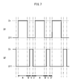
- FIG. 7 is provided in order to explain operation of the DC power supply circuit relating to the second embodiment.
- FIGS. 8A and 8B are circuit diagrams illustrating the DC power supply circuit relating to the second embodiment and flow of current in the DC power supply circuit.
- FIGS. 9A and 9B are circuit diagrams illustrating the DC power supply circuit relating to the second embodiment and flow of current in the DC power supply circuit.
- FIGS. 10A and 10B are circuit diagrams illustrating the DC power supply circuit relating to the second embodiment and flow of current in the DC power supply circuit.
- FIG. 11 illustrates, for the DC power supply circuit relating to the second embodiment, on-off operation of a switching element in section (a), a time series waveform of current flowing through an inductor in section (b), and a time series waveform of current flowing through a diode in section (c).
- FIG. 12 illustrates, for the DC power supply circuit relating to the second embodiment, a time series waveform of output voltage of a rectifier circuit in section (a), a time series waveform of current flowing through the inductor during period P in section (b-1), a time series waveform of current flowing through the diode during period P in section (b-2), a time series waveform of current flowing through the inductor during period Q in section (c-1), and a time series waveform of current flowing through the diode during period Q in section (c-2).
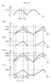
- FIG. 13 illustrates, for the DC power supply circuit relating to the second embodiment, a time series waveform of input voltage to the rectifier circuit from an AC power supply in section (a), a time series waveform of output voltage from the rectifier circuit in section (b), a time series waveform of current flowing through the diode in section (c), and a time series waveform of current flowing from the AC power supply to the rectifier circuit in section (d).
- FIG. 14 illustrates, for a DC power supply circuit relating to a modified example, a time series waveform of current flowing through an inductor when operating in critical mode in section (a-1), a time series waveform of voltage arising at a node between two inductors when operating in critical mode in section (a-2), a time series waveform of current flowing through the inductor when operating in continuous mode in section (b-1), and a time series waveform of voltage arising at the node between the two inductors when operating in continuous mode in section (b-2).
- FIG. 15 illustrates, for a DC power supply circuit relating to a modified example, a time series waveform of input voltage to a rectifier circuit from an AC power supply in section (a), a time series waveform of voltage across terminals of a capacitor in section (b), a time series waveform of voltage at a node between inductors in section (c), and a time series waveform of current flowing from the AC power supply to the rectifier circuit in section (d).
- FIG. 16 is a circuit diagram illustrating a DC power supply circuit relating to a modified example.
- FIGS. 17A and 17B are circuit diagrams illustrating the DC power supply circuit relating to the modified example and flow of current in the DC power supply circuit.
- FIG. 18 is a circuit diagram illustrating a DC power supply circuit relating to a modified example.
- FIGS. 19A and 19B are circuit diagrams illustrating the DC power supply circuit relating to the modified example and flow of current in the DC power supply circuit.
- FIG. 20 is a circuit diagram illustrating a DC power supply circuit relating to a modified example.
- FIG. 21 is a circuit diagram illustrating a DC power supply circuit relating to a modified example.
- FIG. 22 is a circuit diagram illustrating a DC power supply circuit relating to a modified example.
- FIG. 23 is a circuit diagram illustrating a DC power supply circuit relating to a modified example.
- FIG. 24 is a circuit diagram illustrating a DC power supply circuit relating to a modified example.
- FIG. 25 is a circuit diagram illustrating a DC power supply circuit relating to a modified example.
- FIG. 26 is a circuit diagram illustrating a DC power supply circuit relating to a modified example.
- FIG. 27 is a circuit diagram illustrating a DC power supply circuit relating to a modified example.
- FIG. 28 is a circuit diagram illustrating a DC power supply circuit relating to a modified example.
- FIG. 1 is a circuit diagram illustrating a DC power supply circuit 1 relating to the present embodiment.
- the DC power supply circuit 1 includes a rectifier circuit 2 , a voltage conversion circuit 3 , a drive circuit U 1 , and a fixed voltage circuit 4 .
- the rectifier circuit 2 is connected to an alternating current power supply AC.
- the voltage conversion circuit 3 is connected across output terminals of the rectifier circuit 2 .
- the drive circuit U 1 drives the voltage conversion circuit 3 .
- the fixed voltage circuit 4 supplies power to the drive circuit U 1 .
- An output terminal of the voltage conversion circuit 3 is connected to a load 11 , which is formed by a plurality of LEDs connected in series. Voltage across terminals of the load 11 is determined by a number of LEDs included in the load 11 .
- the load 11 differs from a load which has resistive impedance such as a fluorescent lamp.
- the power supply AC outputs AC at a voltage which for example has an actual value of 100 V.
- a current-limiting resistor R 1 is connected between the power supply AC and the rectifier circuit 2 in order to prevent excessive current flowing from the power supply AC to the rectifier circuit 2 .
- the rectifier circuit 2 is a diode bridge composed of four diodes.
- a capacitor C 1 is connected across output terminals of the rectifier circuit 2 in order to block high-frequency noise.
- the capacitor C 1 is for example an electrolytic capacitor, a high dielectric constant ceramic capacitor, or a film capacitor.
- the voltage conversion circuit 3 is a voltage step-up circuit and includes a switching element Q 1 , an inductor (inductor) L 2 , an inductor (auxiliary inductor) L 3 , diodes D 1 and D 2 , capacitors C 2 and C 4 , and a resistor R 2 .
- the switching element Q 1 is an N-channel MOSFET. A source of the switching element Q 1 is connected to an output terminal at a low-potential side of the rectifier circuit 2 , via the resistor R 2 , a gate of the switching element Q 1 is connected to the drive circuit U 1 , via a resistor R 11 , and a drain of the switching element Q 1 is connected to the inductor L 2 .
- the resistor R 2 is provided for detection of drain current flowing in the switching element Q 1 based on voltage arising across terminals of the resistor R 2 .
- a first terminal of the inductor L 2 is connected to the drain of the switching element Q 1 and a second terminal of the inductor L 2 is connected to the inductor L 3 .
- a first terminal of the inductor L 3 is connected to the second terminal of the inductor L 2 and a second terminal of the inductor L 3 is connected to the capacitor C 4 .
- An anode of the diode D 2 is connected to an output terminal at a high-potential side of the rectifier circuit 2 and a cathode of the diode D 2 is connected to the second terminal of the inductor L 2 .
- the diode D 2 is provided in order to prevent reverse flow of current from the second terminal of the inductor L 2 to the capacitor C 1 , which would otherwise occur when flow of current through the inductors L 2 and L 3 stops and electric potential at a node between the inductors L 2 and L 3 becomes greater than electric potential at a high-potential side of the capacitor C 1 .
- the diode D 1 is located in a charging current supply path that supplies current to the capacitor C 2 from between the inductor L 2 and the switching element Q 1 .
- An anode of the diode D 1 is connected to both the first terminal of the inductor L 2 and the drain of the switching element Q 1 , and a cathode of the diode D 1 is connected to the capacitor C 2 .
- a first terminal of the capacitor C 2 is connected to the output terminal at the low-potential side of the rectifier circuit 2 and a second terminal of the capacitor C 2 is connected to the cathode of the diode D 1 .
- a first terminal of the capacitor C 4 is connected to the cathode of the diode D 1 and a second terminal of the capacitor C 4 is connected to the second terminal of the inductor L 3 .
- a current path extending from the second terminal of the capacitor C 2 to the first terminal of the capacitor C 2 , via the load 11 , the inductor L 3 , the inductor L 2 , the switching element Q 1 , and the resistor R 2 in respective order, is a discharge current path for the capacitor C 2 .
- the voltage conversion circuit 3 outputs a voltage across terminals of the capacitor C 4 to the load 11 , which is connected in parallel to the capacitor C 4 .
- the capacitor C 2 is for example an electrolytic capacitor, a high dielectric constant ceramic capacitor, or a film capacitor.
- the drive circuit U 1 outputs a control signal having a rectangular voltage waveform in order to drive the switching element Q 1 through pulse width modulation (PWM) control (herein, the control signal is referred to as a PWM signal).
- PWM pulse width modulation
- the drive circuit U 1 includes a power supply terminal te 0 , an output terminal te 1 , a grounding terminal te 2 , and a current detection terminal te 3 , which is provided in order to detect drain current flowing through the switching element Q 1 .
- the power supply terminal te 0 is connected between output terminals of the fixed voltage circuit 4 .
- the output terminal te 1 is connected to the gate of the switching element Q 1 , via the resistor R 11 .
- the grounding terminal te 2 is connected to the output terminal at the low-potential side of the rectifier circuit 2 .
- the current detection terminal te 3 is connected between the source of the switching element Q 1 and the resistor R 2 .
- the drive circuit U 1 inputs the PWM signal to the gate of the switching element Q 1 and adjusts pulse width of the PWM signal in order that drain current flowing through the switching element Q 1 , which is detected through the current detection terminal te 3 , becomes constant. Adjustment of pulse width of the PWM signal alters a period during which gate voltage of the switching element Q 1 is maintained at equal to or greater than a turn-on voltage of the switching element Q 1 , and a period during which gate voltage of the switching element Q 1 is maintained at less than the turn-on voltage of the switching element Q 1 (i.e., maintained at approximately 0 V).
- the term “turn-on voltage of the switching element Q 1 ” refers to a voltage required between the gate and the source of the switching element Q 1 in order to turn on the switching element Q 1 .
- a period during which the switching element Q 1 is maintained in a turned-on state is referred to as a turned-on period.
- a period during which gate voltage of the switching element Q 1 is maintained at approximately 0 V which in other words is a period in which the switching element Q 1 is maintained in a turned-off state, is referred to as a turned-off period.
- a proportion of the cycle which is made up of the turned-on period is referred to as an “on-duty proportion”.
- the drive circuit U 1 drives the switching element Q 1 through fixed current control by altering the on duty proportion.
- the fixed voltage circuit 4 includes resistors R 41 and R 42 , a capacitor C 43 , and a zener diode ZD 44 .
- the resistors R 41 and R 42 are connected in series across the output terminals of the rectifier circuit 2 .
- a first terminal of the resistor R 41 is connected to the output terminal at the high-potential side of the rectifier circuit 2 .
- the resistor R 42 is connected between a second terminal of the resistor R 41 and the output terminal at the low-potential side of the rectifier circuit 2 .
- the capacitor C 43 is connected across terminals of the resistor R 42 .
- An anode of the zener diode ZD 44 is connected to the output terminal at the low-potential side of the rectifier circuit 2 and a cathode of the zener diode ZD 44 is connected to a node between the resistors R 41 and R 42 , and to the power supply terminal te 0 of the drive circuit U 1 .
- electric potential of the power supply terminal te 0 of the drive circuit U 1 is maintained at a fixed electric potential arising at the cathode of the zener diode ZD 44 .
- the fixed voltage circuit 4 also includes a capacitor C 47 , a resistor R 46 , and diodes D 45 and D 48 .
- a first terminal of the capacitor C 47 is connected to the anode of the diode D 1 of the voltage conversion circuit 3 .
- An anode of the diode D 45 is connected to a second terminal of the capacitor C 47 , via the resistor R 46 , and a cathode of the diode D 45 is connected to the power supply terminal te 0 of the drive circuit U 1 .
- a cathode of the diode D 48 is connected to a node between the resistor R 46 and the anode of the diode D 45 , and an anode of the diode D 48 is connected to the output terminal at the low-potential side of the rectifier circuit 2 .
- the diode D 48 has a function of enabling discharge of electrical charge from the capacitor C 47 .
- FIGS. 2A and 2B are circuit diagrams of the DC power supply circuit 1 relating to the present embodiment, and illustrate flow of current in the DC power supply circuit 1 .
- FIG. 2A illustrates flow of current when the switching element Q 1 is in the turned-on state and FIG. 2B illustrates flow of current when the switching element Q 1 is in the turned-off state.
- a third current path extending from the second terminal of the capacitor C 2 to the first terminal of the capacitor C 2 , via the load 11 , the inductor L 3 , the inductor L 2 , the switching element Q 1 , and the resistor R 2 in respective order.
- the third current path is equivalent to a discharge path for the capacitor C 2 . Discharge of the capacitor C 2 along the third current path causes accumulation of magnetic energy in the inductors L 2 and L 3 , and, at the same time, flow of current along the first current path from the output terminal at the high-potential side of the rectifier circuit 2 causes accumulation of magnetic energy in the inductor L 2 .
- the second current path is equivalent to a charging path for the capacitor C 2 .
- the on-duty proportion of the switching element Q 1 is set in the drive circuit U 1 based on voltage across terminals of the load 11 , number of turns in the inductors L 2 and L 3 (i.e., inductance of the inductors L 2 and L 3 ), and turn ratio of coils in the inductors L 2 and L 3 .
- Voltage arising at the second terminal of the inductor L 2 is set such as to be lower than a voltage (herein, referred to as a threshold voltage) which is lower than output voltage of the rectifier circuit 2 by an amount equal to turn-on voltage Von of the diode D 2 .
- a threshold voltage a voltage which is lower than output voltage of the rectifier circuit 2 by an amount equal to turn-on voltage Von of the diode D 2 .
- section (a) illustrates, for the DC power supply circuit 1 , on-off operation of the switching element Q 1
- section (b) illustrates a time series waveform of current IL 2 flowing through the inductor L 2
- section (c) illustrates a time series waveform of voltage arising at a node for the second terminal of the inductor L 2
- section (d) illustrates a time series waveform of current flowing through the diode D 2 .
- voltage VL of the second terminal of the inductor L 2 is maintained at voltage Vth (herein, referred to as a threshold voltage), which is lower than voltage across terminals of the capacitor C 1 by an amount equal to turn-on voltage of the diode D 2 (period between times T0 and T1 in section (c) of FIG. 3 ).
- Voltage Vth is lower than voltage VC 2 , which arises when current is not flowing through the inductors L 2 and L 3 , by an amount equal to voltage drop VLED of the load 11 .
- Current flowing from the output terminal at the high-potential side of the rectifier circuit 2 to the inductor L 2 , via the diode D 2 also increases gradually (period between times T0 and T1 in section (d) of FIG. 3 ).
- section (a) illustrates, for the DC power supply circuit 1 , a time series waveform of input voltage to the rectifier circuit 2 from the power supply AC
- section (b) illustrates a time series waveform of voltage VC 2 across terminals of the capacitor C 2
- section (c) illustrates a time series waveform of voltage VL of the second terminal of the inductor L 2
- section (d) illustrates a time series waveform of current Iin flowing from the power supply AC to the rectifier circuit 2 .
- the time series waveform of input voltage to the rectifier circuit 2 from the power supply AC is sinusoidal.
- the time series waveform of voltage VC 2 across terminals of the capacitor C 2 has a pulsating shape and times at which maximums of voltage VC 2 occur are shifted relative to times at which maximums of absolute value of input voltage to the rectifier circuit 2 occur.
- Threshold voltage Vth is lower than voltage across terminals of the capacitor C 2 by the amount equal to turn-on voltage Von of the diode D 2 .
- voltage of the second terminal of the inductor L 2 oscillates between threshold voltage Vth and voltage VC 2 -VLED, which is lower than voltage VC 2 across terminals of the capacitor C 2 by an amount equal to voltage drop VLED of the load 11 .
- section (a) illustrates, for the DC power supply circuit 1 , a time series waveform of input voltage to the rectifier circuit 2 from the power supply AC
- section (b) illustrates a time series waveform of voltage VC 2 across terminals of the capacitor C 2
- section (c) illustrates a time series waveform of current Iin flowing from the power supply AC to the rectifier circuit 2 .
- period Ti current flows from the power supply AC to the rectifier circuit 2 .
- period Ts flow of current from the power supply AC to the rectifier circuit 2 is cut-off. Note that in each half cycle of input voltage Vs, a period during which current Iin flows from the power supply AC to the rectifier circuit 2 , even after the absolute value of input voltage Vs has reached a maximum value, is present in period Ti.
- power factor is improved compared to a configuration in which a period does not exist during which current flows from the power supply AC to the rectifier circuit 2 after absolute value of input voltage Vs has reached the maximum value (herein, referred to as a configuration relating to a comparative example).
- power factor in the configuration relating to the comparative example is only in a range from approximately 0.56 to 0.61, whereas the DC power supply circuit 1 relating to the present embodiment enables power factor of 0.8 or greater.
- a time at which input current Iin to the rectifier circuit 2 from the power supply AC is at a maximum value corresponds to a time during a half cycle of input voltage Vs at which approximately a quarter cycle has passed since a start point of the half cycle.
- a time at which input current Iin to the rectifier circuit 2 from the power supply AC is at a maximum value occurs closer to a time at which output voltage Vin of the rectifier circuit 2 is at a maximum value.
- the time series waveform of input current Iin to the DC power supply circuit 1 clearly has improved lateral symmetry compared to the configuration relating to the comparative example.
- the DC power supply circuit 1 there is a reduced amount of shift between times at which input current Iin to the rectifier circuit 2 from the power supply AC is at a maximum value and times at which output voltage Vin is at a maximum value, and lateral symmetry of the time series waveform of input current Iin is improved. Consequently, compared in the configuration relating to the comparative example, in the DC power supply circuit 1 a proportion of input current Iin which is a high-frequency component is reduced.
- An advantageous effect of the above is that emission of high-frequency noise from a device including the DC power supply circuit 1 can be suppressed by an amount corresponding to the aforementioned reduction in the high-frequency component.
- Magnitude of current flowing from the high-potential side of the rectifier circuit 2 to the inductor L 2 when current is flowing through the inductors L 2 and L 3 can be adjusted by adjusting inductance of the inductors L 2 and L 3 .
- the aforementioned current can be increased by increasing inductance of inductor L 2 .
- Increasing inductance of the inductor L 2 enables the inductor L 2 to accumulate a greater amount of energy.
- An increase in inductance of the inductor L 2 is considered to be accompanied by an increase in force causing flow of current from the high-potential side of the rectifier circuit 2 , hence causing an increase in the aforementioned current.
- the DC power supply circuit 1 relating to the present embodiment, during the first period, current flows along the first current path which extends from the output terminal at the high-potential side of the rectifier circuit 2 to the output terminal at the low-potential side of the rectifier circuit 2 , via the inductor L 2 and the switching element Q 1 .
- the second period current flows along the second current path which extends from the output terminal at the high-potential side of the rectifier circuit 2 to the output terminal at the low-potential side of the rectifier circuit 2 , via the inductor L 2 , the charging current supply path, and the capacitor C 2 .
- the first period and the second period are alternately repeated a plurality of times during each half cycle of AC. As a result, current continues to flow from the rectifier circuit 2 to the voltage conversion circuit 3 substantially throughout the entire half cycle of AC, improving power factor relative to the power source AC.
- the DC power supply circuit 1 relating to the present embodiment, current flows from the capacitor C 1 to the inductor L 2 , via the second terminal of inductor L 2 , both when the switching element Q 1 is in the turned-on state (i.e., during the first period) and also when the switching element Q 1 is in the turned-off state (i.e., during the second period).
- the above promotes discharge of the capacitor C 1 such that voltage across terminals of the capacitor C 1 is reduced to less than or equal to output voltage of the rectifier circuit 2 , and thus enables continued supply of current from the power supply AC to the voltage conversion circuit 3 , via the rectifier circuit 2 .
- an amount of time during which current flows from the power supply AC to the capacitor C 1 , via the rectifier circuit 2 can be lengthened, enabling power factor to be improved by a corresponding amount.
- the DC power supply circuit has a configuration in which a power factor correction (PFC) circuit is connected to a rectifier circuit, and a voltage conversion circuit is connected downstream of the PFC circuit.
- the PFC circuit includes elements such as a switching element, an inductor, and a control IC.
- power factor improvement is achieved without providing a PFC circuit. Consequently, the DC power supply circuit 1 relating to the present embodiment enables reduction in circuit size and also enables improved circuit efficiency by eliminating power loss caused by the PFC circuit.
- FIG. 6 is a circuit diagram illustrating a DC power supply circuit 2001 relating to the present embodiment.
- the DC power supply circuit 2001 includes a rectifier circuit 2 , a voltage conversion circuit 2003 , a drive circuit U 2001 , and a fixed voltage circuit 4 .
- the rectifier circuit 2 is connected to an alternating current power supply AC.
- the voltage conversion circuit 2003 is connected across output terminals of the rectifier circuit 2 .
- the drive circuit U 2001 drives the voltage conversion circuit 2003 .
- the fixed voltage circuit 4 supplies power to the drive circuit U 2001 .
- configuration of the voltage conversion circuit 2003 and the drive circuit U 2001 differ to the first embodiment. Note that elements of configuration that are the same as in the first embodiment are labeled using the same reference signs and explanation thereof is omitted where appropriate.
- the voltage conversion circuit 2003 includes a switching element Q 1 (switching element) and a switching element Q 2 (auxiliary switching element), an inductor L 2 , a diode D 2 , a diode bridge (current supply circuit) DB, capacitors C 2 , C 3 , C 4 and C 5 , and a resistor R 2 .
- a first terminal of the capacitor C 2 is connected to an output terminal at a low-potential side of the rectifier circuit 2 .
- the capacitor C 2 is an electrolytic capacitor. Note that alternatively the capacitor C 2 may for example be a high dielectric constant ceramic capacitor or a film capacitor.
- a first terminal of the capacitor (resonance capacitor) C 3 is connected to a second terminal of the capacitor C 2 and a second terminal of the capacitor C 3 is connected to a first input terminal of the diode bridge DB.
- a first terminal of the inductor L 2 is connected to a node between the switching element Q 1 and the switching element Q 2 , and a second terminal of the inductor L 2 is connected to a second input terminal of the diode bridge DB.
- the switching element Q 1 is an N-channel MOSFET.
- a source of the switching element Q 1 is connected to an output terminal at a low-potential side of the rectifier circuit 2 , via the resistor R 2 , a gate of the switching element Q 1 is connected to the drive circuit U 2001 , via the resistor R 11 , and a drain of the switching element Q 1 is connected to the inductor L 2 .
- the switching element Q 2 is located in a charging current supply path for supplying charging current to the capacitor C 2 from between the inductor L 2 and the switching element Q 1 .
- the switching element Q 2 is an N-channel MOSFET.
- a source of the switching element Q 2 is connected to the inductor L 2 and the drain of the switching element Q 1 , a gate of the switching element Q 2 is connected to the drive circuit U 2001 , via the resistor R 12 , and a drain of the switching element Q 2 is connected to the capacitor C 2 .
- the resistor R 2 is provided in order to detect drain current flowing in the switching element Q 1 based on voltage arising across terminals of the resistor R 2 .
- An anode of the diode D 2 is connected to an output terminal at a high-potential side of the rectifier circuit 2 and a cathode of the diode D 2 is connected to a node between the inductor L 2 and the diode bridge DB.
- the capacitor C 4 is connected across the first and second input terminals of the diode bridge DB.
- the capacitor C 4 has a function of smoothing input voltage of the rectifier circuit 2 .
- the first input terminal of the diode bridge DB is connected to the second terminal of the capacitor C 3 .
- a load 11 is connected across two output terminals of the diode bridge DB.
- the diode bridge DB is formed by four diodes Da, Db, Dc, and Dd. Respective cathodes of the diodes Da and Dc are connected to a first terminal of the load 11 , and respective anodes of the diodes Db and Dd are connected to a second terminal of the load 11 .
- An anode of the diode Da is connected to a cathode of the diode Db and an anode of the diode Dc is connected to a cathode of the diode Dd.
- the anode of the diode Da and the cathode of the diode Db are connected to the second terminal of the capacitor C 3 .
- the anode of the diode Dc and the cathode of the diode Dd are connected to the second terminal of the inductor L 2 .
- the capacitor C 5 is connected across the output terminals of the diode bridge DB.
- the capacitor C 5 has a function of smoothing voltage applied to the load 11 .
- the drive circuit U 2001 outputs a control signal having a rectangular voltage waveform in order to drive the switching element Q 1 through PWM control (herein, the control signal is referred to as a PWM signal).
- the drive circuit U 2001 includes a power supply terminal te 0 , a grounding terminal te 2 , a current detection terminal te 3 , and output terminals te 11 and te 12 .
- the power supply terminal te 0 is connected to an output terminal of the fixed voltage circuit 4 .
- the grounding terminal te 2 is connected to the output terminal at the low-potential side of the rectifier circuit 2 .
- the current detection terminal te 3 is provided in order to detect drain current flowing in the switching element Q 1 .
- the current detection terminal te 3 is connected to a node between the source of the switching element Q 1 and the resistor R 2 .
- the output terminal te 11 is connected to the gate of the switching element Q 1 , via the resistor R 11 , and the output terminal te 12 is connected to the gate of the switching element Q 2 , via the resistor R 12 .
- the drive circuit U 2001 is formed as a single integrated circuit.
- the drive circuit U 2001 inputs PWM signals to the respective gates of the switching elements Q 1 and Q 2 , and adjusts pulse width of the PWM signals such that drain current flowing in the switching element Q 1 , which is detected through the current detection terminal te 3 , becomes constant.
- the PWM signal input to the gate of the switching element Q 2 has an opposite phase relative to the PWM signal input to the gate of the switching element Q 1 .
- a change in pulse width of the PWM signal input into the switching element Q 1 causes a change in a proportion of time during which gate voltage of the switching element Q 1 is greater than or equal to turn-on voltage of the switching element Q 1 , which in other words is a proportion of time (herein, referred to as an on-duty proportion) during which the switching element Q 1 is maintained in a turned-on state.
- An on-duty proportion of the switching element Q 2 changes in accordance with the above.
- the drive circuit U 2001 drives the switching element Q 1 as described above through fixed current control.
- the fixed voltage circuit 4 includes the same configuration elements as in the first embodiment.
- a first terminal of a capacitor C 47 is connected to a resistor R 46 and a second terminal of the capacitor C 47 is connected to a node between the switching elements Q 1 and Q 2 in the voltage conversion circuit 2003 .
- a capacitor C 43 and the capacitor C 47 are charged during a period in which the switching element Q 1 is in the turned-off state and the switching element Q 2 is in the turned-on state, and the capacitor C 47 is discharged during a period in which the switching element Q 1 is in the turned-on state and the switching element Q 2 is in the turned-off state, thereby causing electrical charge accumulated in the capacitor C 47 to be transferred to the capacitor C 43 .
- FIG. 7 is a time chart illustrating on-off operation of the switching elements Q 1 and Q 2 in the DC power supply circuit 2001 .
- FIGS. 8A , 8 B, 9 A, 9 B, 10 A, and 10 B are circuit diagrams of the DC power supply circuit 2001 , illustrating flow of current in the DC power supply circuit 2001 .
- period A first period during which the switching element Q 1 is in the turned-on state and the switching element Q 2 is in the turned-off state is followed by period B during which the switching elements Q 1 and Q 2 are both in the turned-off state.
- Period B is followed by period C (second period) during which the switching element Q 1 is in the turned-off state and the switching element Q 2 is in the turned-on state.
- Period C is followed by period D during which, once again, the switching elements Q 1 and Q 2 are both in the turned-off state.
- Periods A to D are repeated in respective order, thereby causing alternate repetition of periods A and C.
- period B is present in which the switching elements Q 1 and Q 2 are both in the turned-off state.
- period D is present in which the switching elements Q 1 and Q 2 are both in the turned-off state.
- period B and period D ensures that at any point in time, at least one of the switching elements Q 1 and Q 2 is in the turned-off state. If a period is present in which the switching elements Q 1 and Q 2 are both in the turned-on state, a malfunction may occur in the DC power supply circuit 2001 .
- FIG. 8A illustrates flow of current during period A, in which the switching element Q 1 is in the turned-on state and the switching element Q 2 is in the turned-off state.
- period A current flows along a path (herein, referred to as a first current path) extending from the output terminal at the high-potential side of the rectifier circuit 2 to the output terminal at the low-potential side of the rectifier circuit 2 , via the inductor L 2 , the switching element Q 1 , and the resistor R 2 .
- a path herein, referred to as a third current path
- current flows along a path (herein, referred to as a third current path) extending from the second terminal of the capacitor C 2 to the first terminal of the capacitor C 2 , via the capacitor C 3 , the diode Da, the load 11 , the diode Dd, the inductor L 2 , the switching element Q 1 , and the resistor R 2 in respective order.
- electric potential at a node between the inductor L 2 and the diode bridge DB is maintained at a magnitude lower than electric potential at the output terminal at the high-potential side of the rectifier circuit 2 by an amount equal to turn-on voltage Von of the diode D 2 .
- the third current path is equivalent to a discharge current path along which electrical charge, previously accumulated in the capacitor C 2 during a period in which the switching element Q 1 was in the turned-off state and the switching element Q 2 was in the turned-on state, is discharged to the load 11 , via the diode bridge DB.
- magnetic energy accumulates in the inductor L 2 as a result of current flowing along the first current path from the output terminal at the high-potential side of the rectifier circuit 2 and discharge current flowing along the third current path from the capacitor C 2 .
- the switching elements Q 1 and Q 2 are both turned off.
- FIG. 8B illustrates flow of current during period B, in which the switching elements Q 1 and Q 2 are both in the turned-off state.
- period B current flows along a path (herein, referred to as current path A) extending from the output terminal at the high-potential side of the rectifier circuit 2 to the output terminal at the low-potential side of the rectifier circuit 2 , via the inductor L 2 , a body diode of the switching element Q 2 , and the capacitor C 2 .
- current path B current flows along a path (herein, referred to as current path B) extending from the first terminal of the inductor L 2 to the second terminal of the inductor L 2 , via the body diode of the switching element Q 2 , the capacitor C 3 , the diode Da, the load 11 , and the diode Dd in respective order.
- FIGS. 9A and 9B illustrate flow of current during period C, in which the switching element Q 1 is in the turned-off state and the switching element Q 2 is in the turned-on state.
- a path (herein, referred to as a second current path) extending from the output terminal at the high-potential side of the rectifier circuit 2 to the output terminal at the low-potential side of the rectifier circuit 2 , via the inductor L 2 , the switching element Q 2 , and the capacitor C 2 .
- current flows along a path (herein, referred to as a fourth current path) extending from the first terminal of the inductor L 2 to the second terminal of the inductor L 2 , via the capacitor C 3 , the diode Da, the load 11 , and the diode Dd in respective order.
- the fourth current path is equivalent to an energy discharge path along which magnetic energy accumulated in the inductor L 2 is discharged to the load 11 , via the diode bridge DB.
- the capacitor C 3 is charged in accompaniment to discharge of magnetic energy accumulated in the inductor L 2 .
- a fifth current path extending from the first terminal of the capacitor C 3 to the second terminal of the capacitor C 3 , via the switching element Q 2 , the inductor L 2 , the diode Dc, the load 11 , and the diode Db in respective order.
- the switching element Q 2 is subsequently turned off such that the switching elements Q 1 and Q 2 are both in the turned-off state.
- FIG. 10A illustrates flow of current during period D, in which the switching elements Q 1 and Q 2 are both in the turned-off state.
- period D current flows along a path (herein, referred to as current path C) from the first terminal of the capacitor C 3 to the second terminal of the capacitor C 3 , via the capacitor C 2 , the resistor R 2 , a body diode of the switching element Q 1 , the inductor L 2 , the diode Dc, the load 11 , and the diode Db in respective order.
- the switching element Q 1 is subsequently turned on.
- FIG. 10B illustrates flow of current during a period (period A), in which the switching element Q 1 is in the turned-on state and the switching element Q 2 is in the turned-off state.
- period A current flows along a path (herein, referred to as a sixth current path) extending from the first terminal of the capacitor C 3 to the second terminal of the capacitor C 3 , via the capacitor C 2 , resistor R 2 , the switching element Q 1 , the inductor L 2 , the diode Dc, the load 11 , and the diode Db in respective order.
- a path herein, referred to as a sixth current path
- section (a) illustrates, for the DC power supply circuit 2001 , on-off operation of the switching elements Q 1 and Q 2
- section (b) illustrates a time series waveform of current IL 2 flowing through the inductor L 2
- section (c) illustrates a time series waveform of current ID 2 flowing through the diode D 2 .
- the phenomenon described above is repeated. Therefore, a period during which current ID 2 flows through the diode D 2 and a period during which current ID 2 is cut-off are alternately repeated.
- the period during which current ID 2 flows through the diode D 2 is in other words period Ti (herein, referred to as a current flow period) during which current flows from the output terminal at the high-potential side of the rectifier circuit 2 to the inductor L 2 .
- the period during which current ID 2 is cut-off is in other words period Ts during which flow of current from the output terminal at the high-potential side of the rectifier circuit 2 to the inductor L 2 is cut-off.
- Length of the period Ti, during which current ID 2 flows through the diode D 2 changes in accordance with instantaneous magnitude of output voltage Vin from the rectifier circuit 2 .
- section (a) illustrates a time series waveform of instantaneous magnitude of output voltage Vin from the rectifier circuit 2
- sections (b-1) and (b-2) respectively illustrate time series waveforms of current IL 2 and current ID 2 flowing respectively through the inductor L 2 and the diode D 2 during period P illustrated in section (a)
- sections (c-1) and (c-2) respectively illustrate time series waveforms of current IL 2 and current ID 2 respectively flowing through the inductor L 2 and the diode D 2 during period Q illustrated in section (a).
- instantaneous magnitude of output voltage Vin from the rectifier circuit 2 is greater during period Q than during period P.
- a single cycle of on-off operation of the switching elements Q 1 and Q 2 , and an on-duty proportion of each of the switching elements Q 1 and Q 2 are set such that a ratio of average values of the aforementioned current flow periods during the single cycle is greater than 0.65.
- the above ensures that a ratio of sum totals of the current flow periods, during a half cycle of AC output from the power supply AC, is greater than 0.65.
- section (a) illustrates, for the DC power supply circuit 2001 , a time series waveform of input voltage Vs to the rectifier circuit 2 from the power supply AC
- section (b) illustrates a time series waveform of output voltage Vin from the rectifier circuit 2
- section (c) illustrates a time series waveform of current ID 2 flowing through the diode D 2
- section (d) illustrates a time series waveform of input current Iin to the rectifier circuit 2 from the power supply AC.
- the time series waveform of input voltage Vs to the rectifier circuit 2 from the power supply AC is sinusoidal, whereas the time series waveform of output voltage Vin from the rectifier circuit 2 has a pulsating shape, maximums of which occur at times coinciding with maximums of absolute value of input voltage Vs to the rectifier circuit 2 from the power supply AC.
- the time series waveform of current ID 2 flowing through the diode D 2 has saw-blade shape which is synchronized with on-off operation of the switching elements Q 1 and Q 2 .
- An envelope around the time series waveform of the current ID 2 increases in accordance with increasing instantaneous magnitude of output voltage Vin from the rectifier circuit 2 .
- Input current Iin to the rectifier circuit 2 from the power supply AC is approximately proportional to current ID 2 flowing through the diode D 2 .
- An increase in instantaneous magnitude of output voltage Vin from the rectifier circuit 2 corresponds to an increase in absolute value of the envelope around the time series waveform of current ID 2 flowing through the diode D 2 .
- absolute value of an envelope around the time series waveform of current Iin, flowing from the power supply AC to the rectifier circuit 2 mirrors absolute value of the envelope around the time series waveform of the current ID 2 flowing through the diode D 2 .
- current Iin continues to flow intermittently from the power supply AC to the rectifier circuit 2 throughout the entirety of each cycle of output voltage Vs of the power supply AC. In other words, current Iin flows intermittently, in synchronization with on-off operation of the switching elements Q 1 and Q 2 , from the power supply AC to the voltage conversion circuit 2003 , via the rectifier circuit 2 .
- the DC power supply circuit 2001 enables circuit efficiency improvement in accordance with an amount of discharge current which is supplied to the load 11 from the capacitor C 2 .
- Charging of the capacitor C 2 is repeated upon each repetition of period C, in which the switching element Q 1 is in the turned-off state and the switching element Q 2 is in the turned-on state, thus maintaining an approximately constant voltage across terminals of the capacitor C 2 . The above enables suppression of variation in magnitude of current supplied to the load 11 from the capacitor C 2 .
- the switching element Q 1 when the switching element Q 1 is in the turned-on state and the switching element Q 2 is in the turned-off state, current flows along the first current path from the output terminal at the high-potential side of the rectifier circuit 2 to the output terminal at the low-potential side of the rectifier circuit 2 and when the switching element Q 1 is in the turned-off state and the switching element Q 2 is in the turned-on state, current flows along the second current path from the output terminal at the high-potential side of the rectifier circuit 2 to the output terminal at the low-potential side of the rectifier circuit 2 .
- the switching elements Q 1 and Q 2 are operated such that period A (first period) and period C (second period) are alternately repeated a plurality of times during each half cycle of AC. As a result, current continues to flow from the rectifier circuit 2 to the voltage conversion circuit 2003 substantially throughout the entire half cycle of AC, thus improving power factor relative to the power supply AC.
- a DC power supply circuit designed in order to improve power factor has a configuration in which a PFC circuit is connected to a rectifier circuit, and a voltage conversion circuit is connected downstream of the PFC circuit.
- the PFC includes elements such as a switching element, an inductor, and a control IC.
- the DC power supply circuit 2001 relating to the present embodiment enables power factor improvement without inclusion of a separate PFC circuit.
- the DC power supply circuit 2001 relating to the present embodiment has advantageous effects of reduced circuit size and improved circuit efficiency through elimination of power loss occurring due to the PFC circuit.
- the DC power supply circuit 2001 is configured using common components such as the diode D 2 and the diode bridge DB, and thus also has an advantageous effect of cost reduction.
- the first embodiment is explained for an example in which the drive circuit U 1 operates the switching element Q 1 in a mode in which periods occur during which current does not flow through the inductors L 2 and L 3 of the voltage conversion circuit 3 (i.e., a so called “discontinuous mode”), but the above is not a limitation.
- the switching element Q 1 may be operated in a so called “critical mode” or “continuous mode” in which current flows through the inductors L 2 and L 3 at all times. In such a situation, operation mode of the drive circuit U 1 can simply be changed while retaining the same configuration as described for the DC power supply circuit 1 in the first embodiment.
- section (a-1) illustrates, for a DC power supply circuit relating to the present modified example, a time series waveform of current IL 2 flowing through the inductor L 2 when the DC power supply circuit is operating in critical mode
- section (a-2) illustrates a time series waveform of voltage arising at the second terminal of the inductor L 2 when the DC power supply circuit is operating in critical mode
- section (b-1) illustrates a time series waveform of current IL 2 flowing through the inductor L 2 when the DC power supply circuit is operating in continuous mode
- section (b-2) illustrates a time series waveform of voltage arising at the second terminal of the inductor L 2 when the DC power supply circuit is operating in continuous mode.
- voltage arising at the second terminal of the inductor L 2 can be maintained at voltage Vth in both critical mode and continuous mode.
- section (a) illustrates, for the DC power supply circuit relating to the present modified example, a time series waveform of input voltage to the rectifier circuit 2 from the power supply AC
- section (b) illustrates a time series waveform of voltage VC 2 across terminals of the capacitor C 2
- section (c) illustrates a time series waveform of voltage VL of the second terminal of the inductor L 2
- section (d) illustrates a time series waveform of current Iin flowing from the power supply AC to the rectifier circuit 2 .
- voltage VLref dasheshed line
- voltage VL of the second terminal of the inductor L 2 is fixed as threshold voltage Vth.
- the voltage conversion circuit 3 is a step-down chopper circuit, but the above is not a limitation.
- the voltage conversion circuit 3 may be a step-up/step-down chopper circuit.
- FIG. 16 is a circuit diagram illustrating a DC power supply circuit 201 relating to the present modified example. Elements of configuration which are the same as in the embodiments are labeled using the same reference signs and explanation thereof is omitted where appropriate.
- voltage conversion circuit 203 is a step-up/step-down chopper circuit, and connection relationship of inductors L 22 and L 23 , and diode D 21 differs from the embodiments.
- a first terminal of a capacitor C 22 is connected to the output terminal at the low-potential side of the rectifier circuit 2 .
- the inductors L 22 and L 23 are connected between the drain of the switching element Q 1 and a second terminal of the capacitor C 22 .
- a first terminal of the inductor L 22 is connected to the drain of the switching element Q 1 .
- a first terminal of the inductor L 23 is connected to the second terminal of the capacitor C 22 and a first terminal of the load 11 , and a second terminal of the inductor L 23 is connected to a second terminal of the inductor L 22 .
- An anode of the diode D 21 is connected to a node between the first terminal of the inductor L 22 and the drain of the switching element Q 1 , and a cathode of the diode D 21 is connected to a second terminal of the load 11 .
- the anode of the diode D 2 is connected to the output terminal at the high-potential side of the rectifier circuit 2 and the cathode of the diode D 2 is connected to the second terminal of the inductor L 22 .
- the capacitor C 24 is an electrolytic capacitor and is connected in parallel to the load 11 .
- FIGS. 17A and 17B are circuit diagrams of the DC power supply circuit 201 relating to the present modified example, illustrating flow of current in the DC power supply circuit 201 . Note that illustration of the fixed voltage circuit 4 is omitted in FIGS. 17A and 17B .
- FIG. 17A illustrates flow of current when the switching element Q 1 is in the turned-on state
- FIG. 17B illustrates flow of current when the switching element Q 1 is in the turned-off state.
- a third current path extending from the second terminal of the capacitor C 22 to the first terminal of the capacitor C 22 , via the inductor L 23 , the inductor L 22 , the switching element Q 1 , and the resistor R 2 in respective order.
- the capacitor C 22 discharges and magnetic energy accumulates in the inductors L 22 and L 23 . Note that power is not supplied to the load 11 during the above.
- the DC power supply circuit 201 is configured such that voltage arising at the second terminal of the inductor L 22 when current flows along the paths illustrated in FIG. 17A is equal to voltage arising at the second terminal of the inductor L 22 when current flows along the paths illustrated in FIG. 17B . More specifically, an on-duty proportion of the switching element Q 1 is set in the drive circuit U 1 based on voltage across terminals of the load 11 , number of turns in the inductors L 22 and L 23 , and turn ratio of coils of the inductors L 22 and L 23 .
- voltage arising at the second terminal of the inductor L 22 is set such as to be lower than a threshold voltage, which is lower than output voltage from the rectifier circuit 2 by an amount equal to turn-on voltage Von of the diode D 2 .
- a threshold voltage which is lower than output voltage from the rectifier circuit 2 by an amount equal to turn-on voltage Von of the diode D 2 .
- the voltage conversion circuit 3 includes the two inductors L 2 and L 3 , but the above is not a limitation.
- the inductor L 3 may be replaced by a diode.
- FIG. 18 is a circuit diagram illustrating a DC power supply circuit 501 relating to the present modified example. Elements of configuration which are the same as in the embodiments are labeled using the same reference signs and explanation thereof is omitted where appropriate.
- voltage conversion circuit 503 is a step-up/step-down chopper circuit, and configuration also differs to the first embodiment in terms that the cathode of the diode D 2 is connected to a node between the inductor L 2 and a cathode of a diode D 503 .
- the first terminal of the inductor L 2 is connected to the drain of the switching element Q 1 and the second terminal of the inductor L 2 is connected to the cathode of the diode D 503 .
- An anode of the diode D 503 is connected to the load 11 .
- the anode of the diode D 2 is connected to the output terminal at the high-potential side of the rectifier circuit 2 and the cathode of the diode D 2 is connected to the node between the inductor L 2 and the cathode of the diode D 503 .
- the diode D 2 has a function of preventing reverse flow of current to the capacitor C 1 from the node between the inductor L 2 and the cathode of the diode D 503 .
- the first terminal of the capacitor C 4 is connected to the cathode of the diode D 1 and the second terminal of the capacitor C 4 is connected to the anode of the diode D 503 .
- the voltage conversion circuit 503 outputs a voltage across terminals of the capacitor C 4 to the load 11 , which is connected in parallel to the capacitor C 4 .
- the capacitor C 2 is for example an electrolytic capacitor, a high dielectric constant ceramic capacitor, or a film capacitor.
- FIGS. 19A and 19B are circuit diagrams of the DC power supply circuit 501 relating to the present modified example, illustrating flow of current in the DC power supply circuit 501 . Note that illustration of the fixed voltage circuit 4 is omitted in FIGS. 19A and 19B .
- FIG. 19A illustrates flow of current when the switching element Q 1 is in the turned-on state
- FIG. 19B illustrates flow of current when the switching element Q 1 is in the turned-off state.
- a third current path extending from the second terminal of the capacitor C 2 to the first terminal of the capacitor C 2 , via the load 11 , the diode D 503 , the inductor L 2 , the switching element Q 1 , and the resistor R 2 in respective order.
- the capacitor C 2 discharges, magnetic energy accumulates in the inductor L 2 , and power is supplied to the load 11 due to current flowing along the third current path.
- the voltage conversion circuit 3 is a non-insulation type voltage conversion circuit such as a step-up chopper circuit, but the above is not a limitation. Alternatively, an insulation type voltage conversion circuit may be provided.
- FIG. 20 is a circuit diagram illustrating a DC power supply circuit 301 relating to the present modified example. Elements of configuration which are the same as in the embodiments are labeled using the same reference signs and explanation thereof is omitted where appropriate.
- voltage conversion circuit 303 is a flyback converter and includes a switching element Q 1 , an inductor L 32 , a transformer TF 33 having a primary coil L 331 and a secondary coil L 332 , diodes D 2 and D 31 , capacitors C 32 and C 34 , and a resistor R 2 .
- polarity of the primary coil L 331 is the opposite of polarity of the secondary coil L 332 .
- a source of the switching element Q 1 is connected to the output terminal at the low-potential side of the rectifier circuit 2 , via the resistor R 2 , a gate of the switching element Q 1 is connected to the drive circuit U 1 , via the resistor R 11 , and a drain of the switching element Q 1 is connected to a first terminal of the inductor L 32 .
- a second terminal of the inductor L 32 is connected to a first terminal of the primary coil L 331 of the transformer TF 33 .
- a second terminal of the primary coil L 331 of the transformer TF 33 is connected to the capacitor C 32 .
- a first terminal of the secondary coil L 332 of the transformer TF 33 is connected to the second terminal of the load 11 , via the diode D 31 , and a second terminal of the secondary coil L 332 is connected to the first terminal of the load 11 .
- the capacitor C 34 is connected in parallel to the load 11 .
- the voltage conversion circuit 303 outputs voltage across terminals of the capacitor C 34 to the load 11 , which is connected in parallel to the capacitor C 34 .
- FIG. 21 is a circuit diagram illustrating a DC power supply circuit 401 relating to the present modified example.
- voltage conversion circuit 403 in the DC power supply circuit 401 includes an inductor L 402 which has a center tap.
- the cathode of the diode D 2 is connected to the center tap of the inductor L 402 .
- magnitude of current flowing from the capacitor C 1 to the inductor L 402 , via the center tap, can be adjusted by changing position of the center tap in the inductor L 402 .
- the present configuration enables reduction in inductor size and thereby also enables reduction in size of the DC power supply circuit as a whole.
- the second embodiment is explained for an example in which the voltage conversion circuit 2003 includes the diode bridge DB, but the above is not a limitation.
- FIG. 22 is a circuit diagram illustrating a DC power supply circuit 2201 relating to the present modified example. Elements of configuration which are the same as in the embodiments are labeled using the same reference signs and explanation thereof is omitted where appropriate.
- voltage conversion circuit 2203 includes a diode D 201 .
- An anode of the diode D 201 is connected to the second terminal of the capacitor C 3 and a cathode of the diode D 201 is connected to the inductor L 2 , via the load 11 .
- the configuration illustrated in FIG. 22 relating to the present modified example enables simplified circuit configuration and reduction in circuit size compared to the DC power supply circuit 2001 relating to the second embodiment.
- FIG. 23 is a circuit diagram illustrating a DC power supply circuit 2301 relating to a different modified example. Elements of configuration which are the same as in the embodiments are labeled using the same reference signs and explanation thereof is omitted where appropriate.
- voltage conversion circuit 2303 includes diodes D 311 and D 312 .
- An anode of the diode D 311 is connected to the second terminal of the capacitor C 3 and a cathode of the diode D 311 is connected to the inductor L 2 , via the load 11 .
- An anode of the diode D 312 is connected to the inductor L 2 , via a load 21 , and a cathode of the diode D 312 is connected to the second terminal of the capacitor C 3 .
- the loads 11 and 21 are each a light-emitting module formed by a plurality of LEDs connected in series.
- a phase of current flowing through the load 11 and a phase of current flowing through the load 21 are shifted relative to one another by precisely a half cycle of the AC, causing the light-emitting module forming the load 11 and the light-emitting module forming the load 21 to repeatedly flash on and off in alternation with one other.
- light output by the light-emitting module forming the load 21 can be used to counterbalance fluctuations in light emitted from the light-emitting module forming the load 11 , by forming a single light-emitting unit from the respective light-emitting modules forming the loads 11 and 21 .
- An advantageous effect of such a configuration is that when the aforementioned light-emitting unit is viewed from a distance, fluctuations in light output from the light-emitting unit are not perceptible.
- the DC power supply circuit 2001 includes the drive circuit U 2001 , which is configured as a single integrated circuit, and the fixed voltage circuit 4 , which supplies power to the drive circuit U 2001 , and in which the DC power supply circuit 2001 operates by a so called “separate excitation” method.
- the DC power supply circuit 2001 may operate by a so called “self excitation” method.
- FIG. 24 is a circuit diagram illustrating a DC power supply circuit 2401 relating to the present modified example. Elements of configuration which are the same as in the second embodiment are labeled using the same reference signs and explanation thereof is omitted where appropriate.
- a voltage conversion circuit 2403 includes switching elements Q 401 and Q 402 , an inductor L 402 , capacitors C 5 , C 402 , C 403 , C 404 and C 468 , diodes D 460 a and D 461 a , and resistors R 467 a and R 467 b .
- the voltage conversion circuit 2403 also includes a transformer Tr 464 , diodes D 453 , D 466 a and D 466 b , a capacitor C 455 , resistors R 452 , R 465 a and R 465 b , and a triac T 454 .
- the transformer Tr 464 has a primary coil L 464 a , a secondary coil L 464 b , and a tertiary coil L 464 c .
- a first terminal of the primary coil L 464 a is connected to the inductor L 402 and a second terminal of the primary coil L 464 a is connected to a first terminal of the secondary coil L 464 b .
- a first terminal of the tertiary coil L 464 c is connected to the output terminal at the low-potential side of the rectifier circuit 2 .
- a first terminal of the capacitor C 402 is connected to the output terminal at the low-potential side of the rectifier circuit 2 .
- a first terminal of the capacitor C 403 is connected to a second terminal of the capacitor C 402 and a second terminal of the capacitor C 403 is connected to a first input terminal of the diode bridge DB.
- a first terminal of the inductor L 402 is connected to the primary coil L 464 a of the transformer Tr 464 and a second terminal of the inductor L 402 is connected to a second input terminal of the diode bridge DB.
- the switching element Q 401 is an N-channel MOSFET.
- a source of the switching element Q 401 is connected to the output terminal at the low-potential side of the rectifier circuit 2 , via the resistor R 467 b , a gate of the switching element Q 401 is connected to a second terminal of the tertiary coil L 464 c of the transformer Tr 464 , and a drain of the switching element Q 401 is connected to the second terminal of the primary coil L 464 a .
- the switching element Q 402 is also an N-channel MOSFET.
- a source of the switching element Q 402 is connected to the second terminal of the primary coil L 464 a , via the resistor R 467 b , a gate of the switching element Q 402 is connected to a second terminal of the secondary coil L 464 b , via the resistor R 465 a , and a drain of the switching element Q 402 is connected to the capacitor C 402 .
- An anode of the diode D 460 a is connected to the output terminal at the low-potential side of the rectifier circuit 2 and a cathode of the diode D 460 a is connected to the second terminal of the primary coil L 464 a.
- An anode of the diode D 461 a is connected to the second terminal of the primary coil L 464 a and a cathode of the diode D 461 a is connected to the second terminal of the capacitor C 402 .
- a first terminal of the capacitor C 468 is connected to the second terminal of the primary coil L 464 a and a second terminal of the capacitor C 468 is connected to the second terminal of the capacitor C 402 .
- An anode of the diode D 453 is connected to the output terminal at the high-potential side of the rectifier circuit 2 , via the resistor R 452 , and a cathode of the diode D 453 is connected to the second terminal of the primary coil L 464 a.
- a first terminal of the capacitor C 455 is connected to the output terminal at the low-potential side of the rectifier circuit 2 and a second terminal of the capacitor C 455 is connected to the anode of the diode D 453 .
- the triac T 454 is connected between the second terminal of the capacitor C 455 and the gate of the switching element Q 401 .
- An anode of the diode D 466 a is connected to the second terminal of the primary coil L 464 a and a cathode of the diode D 466 a is connected to the gate of the switching element Q 402 .
- An anode of the diode D 466 b is connected to the output terminal at the low-potential side of the rectifier circuit 2 and a cathode of the diode D 466 b is connected to the gate of the switching element Q 401 .
- a first terminal of the capacitor C 404 is connected to the second terminal of the capacitor C 403 and a second terminal of the capacitor C 404 is connected to the second terminal of the inductor L 402 .
- the capacitor C 404 has a function of smoothing input voltage to the diode bridge DB.
- configuration elements such as the fixed voltage circuit 4 are not required, enabling simplification of circuit configuration.
- the second embodiment is explained for an example in which the capacitors C 43 and C 47 are charged at the same time as discharge of magnetic energy from the inductor L 2 during a period in which the switching element Q 1 is in the turned-off state and the switching element Q 2 is in the turned-on state. Also, the capacitor C 47 discharges during a period in which the switching element Q 1 is in the turned-on state and the switching element Q 2 is in the turned-off state, thereby causing electrical charge accumulated in the capacitor C 47 to be transferred to the capacitor C 43 .
- the configuration described above is not a limitation.
- a transformer may be included instead of the inductor L 2 such that current flows from a secondary coil of the transformer to the fixed voltage circuit (i.e., charging the fixed voltage circuit).
- FIG. 25 is a circuit diagram illustrating a DC power supply circuit 2501 relating to the present modified example. Elements of configuration which are the same as in the second embodiment are labeled using the same reference signs and explanation thereof is omitted where appropriate.
- voltage conversion circuit 2503 includes a transformer Tr 502 which has a primary coil L 511 and a secondary coil L 512 .
- polarity of the primary coil L 511 is the same as polarity of the secondary coil L 512 .
- Fixed voltage circuit 2504 includes a capacitor C 547 which is connected between the output terminal at the low-potential side of the rectifier circuit 2 and a node between the resistor R 46 and the secondary coil L 512 of the transformer Tr 502 .
- the capacitor C 547 functions as a so called “snubber capacitor” with respect to the secondary coil L 512 .
- the switching element Q 1 is in the turned-off state and the switching element Q 2 is in the turned-on state
- current is supplied from the secondary coil L 512 to the fixed voltage circuit 2504 at the same time as magnetic energy is discharged from the primary coil L 511 . More specifically, current flows from the secondary coil L 512 to the capacitor C 43 , via the resistor R 46 and the diode D 45 , thereby causing charging of the capacitor C 43 .
- the capacitor C 547 may be omitted.
- polarity of the primary coil L 511 is the same as polarity of the secondary coil L 512 , but alternatively polarity of the primary coil L 511 may be the opposite of polarity of the secondary coil L 512 .
- current is supplied from the secondary coil L 512 to the fixed voltage circuit 2504 at the same time as magnetic energy is accumulated in the primary coil L 511 .
- FIG. 26 is a circuit diagram illustrating a DC power supply circuit 2601 relating to a different modified example. Elements of configuration which are the same as in FIG. 25 are labeled using the same reference signs and explanation thereof is omitted where appropriate.
- the DC power supply circuit 2601 differs from the configuration illustrated in FIG. 25 in terms that voltage conversion circuit 2603 includes a diode bridge DB 2 which has input terminals connected across the first and second terminals of the secondary coil L 512 in the transformer Tr 502 .
- An output terminal at a high-potential side of the diode bridge DB 2 is connected to the fixed voltage circuit 2504 and an output terminal at a low-potential side of the diode bridge DB 2 is connected to the output terminal at the low-potential side of the rectifier circuit 2 .
- polarity of the primary coil L 511 may alternatively be the opposite of polarity of the secondary coil L 512 .
- power may for example be supplied to the fixed voltage circuit 2504 when voltage at a node between the transformer Tr 502 and the switching element Q 1 is no greater than a certain voltage during a period in which the switching element Q 1 is in the turned-off state.
- FIG. 27 is a circuit diagram illustrating a DC power supply circuit 2701 relating to a different modified example. Elements of configuration which are the same as in the embodiments are labeled using the same reference signs and explanation thereof is omitted where appropriate.
- a switching element Q 702 is connected between a fixed voltage circuit 2704 and the node between the inductor L 2 and the switching element Q 1 in the voltage conversion circuit 2003 .
- the DC power supply circuit 2701 includes a drive circuit U 2002 , which has a control terminal te 4 for outputting a signal voltage for controlling the switching element Q 702 .
- the switching element Q 702 is an N-channel MOSFET.
- a source of the switching element Q 702 is connected to the fixed voltage circuit 2704
- a gate of the switching element Q 702 is connected to the control terminal te 4 of the drive circuit U 2002 , via a resistor R 712
- a drain of the switching element Q 702 is connected to a node between the switching elements Q 1 and Q 2 .
- a resistor R 46 is directly connected to the source of the switching element Q 702 .
- the fixed voltage circuit 2704 has the same configuration as the fixed voltage circuit 2504 illustrated in FIG. 25 but with the capacitor C 547 omitted therefrom.
- the switching element Q 702 is set in the turned-on state through a signal voltage from the control terminal te 4 , which is a certain voltage that is greater than 0 V. Timing at which the switching element Q 702 is turned on is set in advance. As a result, power loss in the resistor R 46 of the fixed voltage circuit 2704 can be reduced, enabling improved circuit efficiency. Furthermore, a number of circuit elements can be reduced in the fixed voltage circuit 2704 , thereby enabling reduction in circuit size.
- a noise filter 2005 including an inductor NF and capacitors C 0 and C 1 , may be provided between the DC power supply circuit 2001 and the power supply AC as illustrated in FIG. 28A .
- a DC power supply circuit 2801 may include a noise filter 2205 between the rectifier circuit 2 and the voltage conversion circuit 2003 .
- the noise filter 2205 includes a capacitor connected across output terminals of the rectifier circuit 2 and an inductor NF connected in series between the capacitor and the voltage conversion circuit 2003 (i.e., the diode D 2 illustrated in FIG. 6 ).
- position at which the noise filter is connected is preferably altered in a situation in which an objective is high-frequency ripple reduction compared to a situation in which an objective is high-frequency noise reduction.
- the capacitor C 1 should be connected to a terminal of inductor NF which is closest to the voltage conversion circuit 2003 .
- two capacitors may be provided connected to opposite terminals of the inductor NF.
- an additional inductor NF may be provided connected to the low-potential side of the rectifier circuit 2 .
- the second embodiment was explained for an example in which the DC power supply circuit 2001 includes the diode bridge DB as a current supply circuit, but the above is not a limitation.
- a current supply circuit may simply be formed by a wire connecting the second terminal of the capacitor C 2 and the second terminal of the load 11 , and by a wire connecting the second terminal of the inductor L 2 and the first terminal of the load 11 .
- the first embodiment and the second embodiment are explained for examples in which the switching element Q 1 in the voltage conversion circuit 3 and the switching elements Q 1 and Q 2 in the voltage conversion circuit 2003 are N-channel MOSFETs, but the above is not a limitation, and alternatively the aforementioned switching elements may be P-channel MOSFETs. Further alternatively, the aforementioned switching elements may be bipolar transistors.
- a configuration may be adopted in which a power adjuster is provided between the power supply AC and the DC power supply circuit 1 in order to adjust power input to the DC power supply circuit 1 .
- a power adjustor may be provided between the power supply AC and the DC power supply circuit 2001 .
- the power adjustor may typically include a triac or the like, and there is a possibility of a malfunction occurring in the triac if current flows toward the DC power supply circuit 1 while input voltage to the DC power supply circuit 1 is zero.
- phase of input voltage approximately matches phase of input current in the DC power supply circuit 1 , and input current is caused to flow even at low input voltage close to crossing zero.
- power adjustor malfunction is prevented in the configuration described above in which the power adjustor includes the triac.
Abstract
Description
- [Patent Literature 1] Japanese Unexamined Patent Application Publication No. 2011-90901
-
- 1, 201, 301, 2001, 2201, 2301, 2401, 2501, 2601, 2701, 2801 DC power supply circuit
- 2 rectifier circuit
- 3, 203, 2003, 2203, 2303, 2403, 2503, 2603 voltage conversion circuit
- 4, 504, 2704 fixed voltage circuit
- 11, 21 load
- 2005, 2205 noise filter
- C0, C2, C3, C4, C5, C22, C24, C32, C34, C43, C47, C402, C403, C404, C455, C468, C547 capacitor
- D1, D2, D3, D21, D31, D45, D48, D201, D311, D312, D453, D460 a, D461 a, D466 a, D466 b diode
- DB, DB2 diode bridge
- L2, L3, L22, L23, L32, L402 inductor
- L331, L464 a, L511 primary coil
- L332, L464 b, L512 secondary coil
- L464 c tertiary coil
- Q1, Q2, Q401, Q402, Q702 switching element
- R1, R2, R11, R12, R41, R42, R46, R452, R465 a, R467 a, R467 b, R712 resistor
- T454 triac
- TF33, Tr464, Tr502 transformer
- U1, U2001, U2002 drive circuit
- ZD44 zener diode
Claims (12)
Applications Claiming Priority (7)
| Application Number | Priority Date | Filing Date | Title |
|---|---|---|---|
| JP2012026050 | 2012-02-09 | ||
| JP2012-026050 | 2012-02-09 | ||
| JP2012034804 | 2012-02-21 | ||
| JP2012-034804 | 2012-02-21 | ||
| JP2012052588 | 2012-03-09 | ||
| JP2012-052588 | 2012-03-09 | ||
| PCT/JP2012/006656 WO2013124921A1 (en) | 2012-02-21 | 2012-10-18 | Dc power supply circuit |
Publications (2)
| Publication Number | Publication Date |
|---|---|
| US20150009728A1 US20150009728A1 (en) | 2015-01-08 |
| US9257901B2 true US9257901B2 (en) | 2016-02-09 |
Family
ID=49005145
Family Applications (1)
| Application Number | Title | Priority Date | Filing Date |
|---|---|---|---|
| US14/376,984 Expired - Fee Related US9257901B2 (en) | 2012-02-09 | 2012-10-18 | DC power supply circuit |
Country Status (4)
| Country | Link |
|---|---|
| US (1) | US9257901B2 (en) |
| EP (1) | EP2819292B1 (en) |
| JP (1) | JP5250163B1 (en) |
| WO (1) | WO2013124921A1 (en) |
Cited By (1)
| Publication number | Priority date | Publication date | Assignee | Title |
|---|---|---|---|---|
| WO2021221680A1 (en) * | 2020-04-30 | 2021-11-04 | Hewlett-Packard Development Company, L.P. | Dynamically altering capacitance value of capacitors |
Families Citing this family (7)
| Publication number | Priority date | Publication date | Assignee | Title |
|---|---|---|---|---|
| KR101386830B1 (en) * | 2012-05-29 | 2014-04-29 | 엘에스산전 주식회사 | Power factor correction circuit |
| PL3028376T3 (en) * | 2013-07-29 | 2022-10-31 | Sma Solar Technology Ag | Step-up converter, corresponding inverter and method of operation |
| CN105207472A (en) * | 2015-10-27 | 2015-12-30 | 杰华特微电子(杭州)有限公司 | Circuit used for boosting buck output voltage |
| WO2017134824A1 (en) * | 2016-02-05 | 2017-08-10 | 俊蔵 大島 | Power supply device |
| US10540040B2 (en) * | 2016-06-30 | 2020-01-21 | Stmicroelectronics Asia Pacific Pte Ltd | Architecture and driving methods for minimizing power losses in touch panel |
| JP6340463B1 (en) * | 2017-09-26 | 2018-06-06 | 高周波熱錬株式会社 | Power supply |
| US11863062B2 (en) * | 2018-04-27 | 2024-01-02 | Raytheon Company | Capacitor discharge circuit |
Citations (15)
| Publication number | Priority date | Publication date | Assignee | Title |
|---|---|---|---|---|
| DE19633351A1 (en) | 1995-08-19 | 1997-02-20 | Toko Inc | Power factor improvement circuit e.g. for electronic device power supply |
| JP2000071070A (en) | 1998-07-09 | 2000-03-07 | Illinois Tool Works Inc <Itw> | Welding power source and welding power supplying method |
| US20040125625A1 (en) * | 2002-06-28 | 2004-07-01 | Nillesen Martijn E. | Method and apparatus for controlling the power supplied to a load |
| US6865096B1 (en) | 1998-07-09 | 2005-03-08 | Illinois Tool Works Inc. | Power convertor with low loss switching |
| JP2005142137A (en) | 2003-10-15 | 2005-06-02 | Matsushita Electric Works Ltd | Led lighting device |
| JP2006034028A (en) | 2004-07-20 | 2006-02-02 | Matsushita Electric Ind Co Ltd | Power conversion apparatus, motor driving device, and air conditioner |
| US20100118572A1 (en) * | 2008-11-12 | 2010-05-13 | Alexander Mednik | Led driver with low harmonic distortion of input ac current and methods of controlling the same |
| US20100265745A1 (en) * | 2009-04-16 | 2010-10-21 | Fsp Technology Inc. | Parameter configuration method for elements of power factor correction function converter |
| US20100265231A1 (en) * | 2009-04-15 | 2010-10-21 | Hyeon-Yong Jang | Method of supplying power, power supply apparatus for performing the method and display apparatus having the apparatus |
| JP2011090901A (en) | 2009-10-22 | 2011-05-06 | Phoenix Electric Co Ltd | Power supply circuit |
| JP2012023294A (en) | 2010-07-16 | 2012-02-02 | Time Engineering Co Ltd | Led lighting device |
| US20120081032A1 (en) | 2010-09-30 | 2012-04-05 | Taiwan Semiconductor Manufacturing Company, Ltd. | Mechanisms for anti-flickering |
| EP2458722A1 (en) | 2010-11-24 | 2012-05-30 | Samsung LED Co., Ltd. | LED driving apparatus |
| WO2013128509A1 (en) | 2012-03-02 | 2013-09-06 | パナソニック株式会社 | Dc power supply circuit |
| WO2013128506A1 (en) | 2012-03-01 | 2013-09-06 | パナソニック株式会社 | Dc power supply circuit |
-
2012
- 2012-10-18 JP JP2013505257A patent/JP5250163B1/en not_active Expired - Fee Related
- 2012-10-18 US US14/376,984 patent/US9257901B2/en not_active Expired - Fee Related
- 2012-10-18 EP EP12869175.5A patent/EP2819292B1/en not_active Not-in-force
- 2012-10-18 WO PCT/JP2012/006656 patent/WO2013124921A1/en active Application Filing
Patent Citations (23)
| Publication number | Priority date | Publication date | Assignee | Title |
|---|---|---|---|---|
| DE19633351A1 (en) | 1995-08-19 | 1997-02-20 | Toko Inc | Power factor improvement circuit e.g. for electronic device power supply |
| US5740022A (en) | 1995-08-19 | 1998-04-14 | Toko, Inc. | Power factor improving circuit |
| US20050185432A1 (en) | 1998-07-09 | 2005-08-25 | Illinois Tool Works Inc. | Power convertor with low loss switching |
| US6115273A (en) | 1998-07-09 | 2000-09-05 | Illinois Tool Works Inc. | Power converter with low loss switching |
| US6266257B1 (en) | 1998-07-09 | 2001-07-24 | Illinois Tool Works Inc. | Power convertor with low loss switching |
| US20010026458A1 (en) | 1998-07-09 | 2001-10-04 | Illinois Tool Works Inc. | Power convertor with low loss switching |
| US20020191425A1 (en) | 1998-07-09 | 2002-12-19 | Illinois Tool Works Inc. | Power convertor with low loss switching |
| US6865096B1 (en) | 1998-07-09 | 2005-03-08 | Illinois Tool Works Inc. | Power convertor with low loss switching |
| JP2000071070A (en) | 1998-07-09 | 2000-03-07 | Illinois Tool Works Inc <Itw> | Welding power source and welding power supplying method |
| US20080298102A1 (en) | 1998-07-09 | 2008-12-04 | Illinois Toolworks Inc. | Power Converter With Low Loss Switching |
| US20040125625A1 (en) * | 2002-06-28 | 2004-07-01 | Nillesen Martijn E. | Method and apparatus for controlling the power supplied to a load |
| JP2005142137A (en) | 2003-10-15 | 2005-06-02 | Matsushita Electric Works Ltd | Led lighting device |
| JP2006034028A (en) | 2004-07-20 | 2006-02-02 | Matsushita Electric Ind Co Ltd | Power conversion apparatus, motor driving device, and air conditioner |
| US20100118572A1 (en) * | 2008-11-12 | 2010-05-13 | Alexander Mednik | Led driver with low harmonic distortion of input ac current and methods of controlling the same |
| US20100265231A1 (en) * | 2009-04-15 | 2010-10-21 | Hyeon-Yong Jang | Method of supplying power, power supply apparatus for performing the method and display apparatus having the apparatus |
| US20100265745A1 (en) * | 2009-04-16 | 2010-10-21 | Fsp Technology Inc. | Parameter configuration method for elements of power factor correction function converter |
| JP2011090901A (en) | 2009-10-22 | 2011-05-06 | Phoenix Electric Co Ltd | Power supply circuit |
| JP2012023294A (en) | 2010-07-16 | 2012-02-02 | Time Engineering Co Ltd | Led lighting device |
| US20120081032A1 (en) | 2010-09-30 | 2012-04-05 | Taiwan Semiconductor Manufacturing Company, Ltd. | Mechanisms for anti-flickering |
| EP2458722A1 (en) | 2010-11-24 | 2012-05-30 | Samsung LED Co., Ltd. | LED driving apparatus |
| WO2013128506A1 (en) | 2012-03-01 | 2013-09-06 | パナソニック株式会社 | Dc power supply circuit |
| WO2013128509A1 (en) | 2012-03-02 | 2013-09-06 | パナソニック株式会社 | Dc power supply circuit |
| US20150036401A1 (en) | 2012-03-02 | 2015-02-05 | Panasonic Corporation | Dc power supply circuit |
Non-Patent Citations (4)
| Title |
|---|
| Extended European Search Report for corresponding European Application No. EP 12 86 9175 dated Feb. 18, 2015. |
| Extended European Search Report for corresponding European Application No. EP 12 86 9175 dated Feb. 27, 2015 (previously submitted on IDS filed May 26, 2015). |
| Form PCT/ISA/237 for corresponding International Application No. PCT/JP2012/006656 dated Jan. 22, 2013. |
| International Search Report for corresponding International Application No. PCT/JP2012/006656 mailed Jan. 22, 2013. |
Cited By (1)
| Publication number | Priority date | Publication date | Assignee | Title |
|---|---|---|---|---|
| WO2021221680A1 (en) * | 2020-04-30 | 2021-11-04 | Hewlett-Packard Development Company, L.P. | Dynamically altering capacitance value of capacitors |
Also Published As
| Publication number | Publication date |
|---|---|
| EP2819292B1 (en) | 2017-12-06 |
| EP2819292A1 (en) | 2014-12-31 |
| JP5250163B1 (en) | 2013-07-31 |
| WO2013124921A1 (en) | 2013-08-29 |
| US20150009728A1 (en) | 2015-01-08 |
| EP2819292A4 (en) | 2015-04-01 |
| JPWO2013124921A1 (en) | 2015-05-21 |
Similar Documents
| Publication | Publication Date | Title |
|---|---|---|
| US11323036B2 (en) | Forward converter having a primary-side current sense circuit | |
| US9257901B2 (en) | DC power supply circuit | |
| US9515547B2 (en) | DC power supply circuit | |
| EP2536013B1 (en) | A cascade boost and inverting buck converter | |
| JP5693870B2 (en) | Switching power supply circuit | |
| US9491820B2 (en) | Hybrid dimming control techniques for LED drivers | |
| EP3050400B1 (en) | Electronic resonant and insulated half-bridge zeta converter and method to control the converter | |
| US8188617B2 (en) | Current balancing apparatus, current balancing method, and power supply apparatus | |
| US9093893B2 (en) | DC power supply circuit | |
| WO2013172259A1 (en) | Switching power supply circuit and led lighting device | |
| WO2012144274A1 (en) | Led lighting device and led illuminating device | |
| US9426869B2 (en) | Multi-output electronic ballast | |
| JP5260809B1 (en) | DC power supply circuit | |
| JP2014110196A (en) | Lighting device and illuminating fixture |
Legal Events
| Date | Code | Title | Description |
|---|---|---|---|
| AS | Assignment |
Owner name: PANASONIC CORPORATION, JAPAN Free format text: ASSIGNMENT OF ASSIGNORS INTEREST;ASSIGNORS:SUGITA, KAZUSHIGE;ITOH, KAZUHIKO;MURAKAMI, MASANOBU;SIGNING DATES FROM 20140507 TO 20140519;REEL/FRAME:033715/0523 |
|
| AS | Assignment |
Owner name: PANASONIC INTELLECTUAL PROPERTY MANAGEMENT CO., LTD., JAPAN Free format text: ASSIGNMENT OF ASSIGNORS INTEREST;ASSIGNOR:PANASONIC CORPORATION;REEL/FRAME:034194/0143 Effective date: 20141110 Owner name: PANASONIC INTELLECTUAL PROPERTY MANAGEMENT CO., LT Free format text: ASSIGNMENT OF ASSIGNORS INTEREST;ASSIGNOR:PANASONIC CORPORATION;REEL/FRAME:034194/0143 Effective date: 20141110 |
|
| STCF | Information on status: patent grant |
Free format text: PATENTED CASE |
|
| FEPP | Fee payment procedure |
Free format text: MAINTENANCE FEE REMINDER MAILED (ORIGINAL EVENT CODE: REM.); ENTITY STATUS OF PATENT OWNER: LARGE ENTITY |
|
| LAPS | Lapse for failure to pay maintenance fees |
Free format text: PATENT EXPIRED FOR FAILURE TO PAY MAINTENANCE FEES (ORIGINAL EVENT CODE: EXP.); ENTITY STATUS OF PATENT OWNER: LARGE ENTITY |
|
| STCH | Information on status: patent discontinuation |
Free format text: PATENT EXPIRED DUE TO NONPAYMENT OF MAINTENANCE FEES UNDER 37 CFR 1.362 |
|
| FP | Lapsed due to failure to pay maintenance fee |
Effective date: 20200209 |
|
| AS | Assignment |
Owner name: PANASONIC INTELLECTUAL PROPERTY MANAGEMENT CO., LTD., JAPAN Free format text: CORRECTIVE ASSIGNMENT TO CORRECT THE ERRONEOUSLY FILED APPLICATION NUMBERS 13/384239, 13/498734, 14/116681 AND 14/301144 PREVIOUSLY RECORDED ON REEL 034194 FRAME 0143. ASSIGNOR(S) HEREBY CONFIRMS THE ASSIGNMENT;ASSIGNOR:PANASONIC CORPORATION;REEL/FRAME:056788/0362 Effective date: 20141110 |