US9349637B2 - Method for void-free cobalt gap fill - Google Patents
Method for void-free cobalt gap fill Download PDFInfo
- Publication number
- US9349637B2 US9349637B2 US14/465,610 US201414465610A US9349637B2 US 9349637 B2 US9349637 B2 US 9349637B2 US 201414465610 A US201414465610 A US 201414465610A US 9349637 B2 US9349637 B2 US 9349637B2
- Authority
- US
- United States
- Prior art keywords
- cobalt
- feature
- features
- substrate
- plasma
- Prior art date
- Legal status (The legal status is an assumption and is not a legal conclusion. Google has not performed a legal analysis and makes no representation as to the accuracy of the status listed.)
- Active
Links
- GUTLYIVDDKVIGB-UHFFFAOYSA-N cobalt atom Chemical compound [Co] GUTLYIVDDKVIGB-UHFFFAOYSA-N 0.000 title claims abstract description 216
- 229910017052 cobalt Inorganic materials 0.000 title claims abstract description 207
- 239000010941 cobalt Substances 0.000 title claims abstract description 206
- 238000000034 method Methods 0.000 title claims abstract description 146
- 238000000151 deposition Methods 0.000 claims abstract description 55
- 239000002243 precursor Substances 0.000 claims abstract description 51
- 239000007789 gas Substances 0.000 claims abstract description 50
- 238000010899 nucleation Methods 0.000 claims abstract description 39
- 230000006911 nucleation Effects 0.000 claims abstract description 39
- 230000004888 barrier function Effects 0.000 claims abstract description 29
- 238000005229 chemical vapour deposition Methods 0.000 claims abstract description 25
- QJGQUHMNIGDVPM-UHFFFAOYSA-N nitrogen group Chemical group [N] QJGQUHMNIGDVPM-UHFFFAOYSA-N 0.000 claims abstract description 21
- 239000000758 substrate Substances 0.000 claims description 96
- 239000003638 chemical reducing agent Substances 0.000 claims description 28
- -1 tungsten nitride Chemical class 0.000 claims description 28
- 230000002401 inhibitory effect Effects 0.000 claims description 11
- 230000005764 inhibitory process Effects 0.000 claims description 10
- 229910052721 tungsten Inorganic materials 0.000 claims description 9
- 239000010937 tungsten Substances 0.000 claims description 9
- WFKWXMTUELFFGS-UHFFFAOYSA-N tungsten Chemical compound [W] WFKWXMTUELFFGS-UHFFFAOYSA-N 0.000 claims description 7
- NRTOMJZYCJJWKI-UHFFFAOYSA-N Titanium nitride Chemical compound [Ti]#N NRTOMJZYCJJWKI-UHFFFAOYSA-N 0.000 claims description 3
- 239000010936 titanium Substances 0.000 claims description 3
- KJTLSVCANCCWHF-UHFFFAOYSA-N Ruthenium Chemical compound [Ru] KJTLSVCANCCWHF-UHFFFAOYSA-N 0.000 claims description 2
- RTAQQCXQSZGOHL-UHFFFAOYSA-N Titanium Chemical group [Ti] RTAQQCXQSZGOHL-UHFFFAOYSA-N 0.000 claims description 2
- 229910052707 ruthenium Inorganic materials 0.000 claims description 2
- 229910052715 tantalum Inorganic materials 0.000 claims description 2
- GUVRBAGPIYLISA-UHFFFAOYSA-N tantalum atom Chemical compound [Ta] GUVRBAGPIYLISA-UHFFFAOYSA-N 0.000 claims description 2
- MZLGASXMSKOWSE-UHFFFAOYSA-N tantalum nitride Chemical compound [Ta]#N MZLGASXMSKOWSE-UHFFFAOYSA-N 0.000 claims description 2
- 229910052719 titanium Inorganic materials 0.000 claims description 2
- 238000011049 filling Methods 0.000 abstract description 3
- 230000008569 process Effects 0.000 description 88
- 230000008021 deposition Effects 0.000 description 36
- 238000012545 processing Methods 0.000 description 36
- 238000011282 treatment Methods 0.000 description 28
- 235000012431 wafers Nutrition 0.000 description 23
- IJGRMHOSHXDMSA-UHFFFAOYSA-N Atomic nitrogen Chemical compound N#N IJGRMHOSHXDMSA-UHFFFAOYSA-N 0.000 description 21
- 238000000231 atomic layer deposition Methods 0.000 description 15
- 229910052757 nitrogen Inorganic materials 0.000 description 15
- NJPPVKZQTLUDBO-UHFFFAOYSA-N novaluron Chemical compound C1=C(Cl)C(OC(F)(F)C(OC(F)(F)F)F)=CC=C1NC(=O)NC(=O)C1=C(F)C=CC=C1F NJPPVKZQTLUDBO-UHFFFAOYSA-N 0.000 description 15
- 230000001276 controlling effect Effects 0.000 description 14
- 238000004519 manufacturing process Methods 0.000 description 14
- 239000004065 semiconductor Substances 0.000 description 14
- 239000012159 carrier gas Substances 0.000 description 11
- 229910052751 metal Inorganic materials 0.000 description 8
- 239000002184 metal Substances 0.000 description 8
- 239000000463 material Substances 0.000 description 7
- 238000002474 experimental method Methods 0.000 description 6
- 238000011112 process operation Methods 0.000 description 6
- 238000005530 etching Methods 0.000 description 5
- 239000000203 mixture Substances 0.000 description 5
- 238000009832 plasma treatment Methods 0.000 description 5
- 238000012546 transfer Methods 0.000 description 5
- 239000011800 void material Substances 0.000 description 5
- XKRFYHLGVUSROY-UHFFFAOYSA-N Argon Chemical compound [Ar] XKRFYHLGVUSROY-UHFFFAOYSA-N 0.000 description 4
- UGFAIRIUMAVXCW-UHFFFAOYSA-N Carbon monoxide Chemical compound [O+]#[C-] UGFAIRIUMAVXCW-UHFFFAOYSA-N 0.000 description 4
- XUIMIQQOPSSXEZ-UHFFFAOYSA-N Silicon Chemical compound [Si] XUIMIQQOPSSXEZ-UHFFFAOYSA-N 0.000 description 4
- 229910002091 carbon monoxide Inorganic materials 0.000 description 4
- 238000005137 deposition process Methods 0.000 description 4
- 238000009713 electroplating Methods 0.000 description 4
- 239000007788 liquid Substances 0.000 description 4
- 229910052710 silicon Inorganic materials 0.000 description 4
- 239000010703 silicon Substances 0.000 description 4
- 238000003860 storage Methods 0.000 description 4
- 125000000217 alkyl group Chemical group 0.000 description 3
- 125000000484 butyl group Chemical group [H]C([*])([H])C([H])([H])C([H])([H])C([H])([H])[H] 0.000 description 3
- 239000004020 conductor Substances 0.000 description 3
- 238000010586 diagram Methods 0.000 description 3
- 238000010438 heat treatment Methods 0.000 description 3
- 125000001183 hydrocarbyl group Chemical group 0.000 description 3
- 239000001257 hydrogen Substances 0.000 description 3
- 229910052739 hydrogen Inorganic materials 0.000 description 3
- 238000001459 lithography Methods 0.000 description 3
- 238000002161 passivation Methods 0.000 description 3
- 229920002120 photoresistant polymer Polymers 0.000 description 3
- 125000001436 propyl group Chemical group [H]C([*])([H])C([H])([H])C([H])([H])[H] 0.000 description 3
- 239000000376 reactant Substances 0.000 description 3
- 238000001878 scanning electron micrograph Methods 0.000 description 3
- 238000002207 thermal evaporation Methods 0.000 description 3
- 125000004209 (C1-C8) alkyl group Chemical group 0.000 description 2
- 125000003903 2-propenyl group Chemical group [H]C([*])([H])C([H])=C([H])[H] 0.000 description 2
- UFHFLCQGNIYNRP-UHFFFAOYSA-N Hydrogen Chemical compound [H][H] UFHFLCQGNIYNRP-UHFFFAOYSA-N 0.000 description 2
- VYPSYNLAJGMNEJ-UHFFFAOYSA-N Silicium dioxide Chemical compound O=[Si]=O VYPSYNLAJGMNEJ-UHFFFAOYSA-N 0.000 description 2
- 229910052786 argon Inorganic materials 0.000 description 2
- 230000015572 biosynthetic process Effects 0.000 description 2
- 239000012707 chemical precursor Substances 0.000 description 2
- 238000006243 chemical reaction Methods 0.000 description 2
- 230000001934 delay Effects 0.000 description 2
- 230000000694 effects Effects 0.000 description 2
- 125000001495 ethyl group Chemical group [H]C([H])([H])C([H])([H])* 0.000 description 2
- 125000003187 heptyl group Chemical group [H]C([*])([H])C([H])([H])C([H])([H])C([H])([H])C([H])([H])C([H])([H])C([H])([H])[H] 0.000 description 2
- 125000004051 hexyl group Chemical group [H]C([H])([H])C([H])([H])C([H])([H])C([H])([H])C([H])([H])C([H])([H])* 0.000 description 2
- 238000011065 in-situ storage Methods 0.000 description 2
- 239000003446 ligand Substances 0.000 description 2
- 230000033001 locomotion Effects 0.000 description 2
- 230000007246 mechanism Effects 0.000 description 2
- 125000002496 methyl group Chemical group [H]C([H])([H])* 0.000 description 2
- 125000002347 octyl group Chemical group [H]C([*])([H])C([H])([H])C([H])([H])C([H])([H])C([H])([H])C([H])([H])C([H])([H])C([H])([H])[H] 0.000 description 2
- 125000000962 organic group Chemical group 0.000 description 2
- 150000002902 organometallic compounds Chemical class 0.000 description 2
- 125000001147 pentyl group Chemical group C(CCCC)* 0.000 description 2
- 238000005240 physical vapour deposition Methods 0.000 description 2
- 238000000623 plasma-assisted chemical vapour deposition Methods 0.000 description 2
- 238000011160 research Methods 0.000 description 2
- 0 CC(C)(C)c12c[Co]1(C=O)(C=O)(C=O)c2 Chemical compound CC(C)(C)c12c[Co]1(C=O)(C=O)(C=O)c2 0.000 description 1
- 229910018874 CoNx Inorganic materials 0.000 description 1
- 229910052581 Si3N4 Inorganic materials 0.000 description 1
- 238000003848 UV Light-Curing Methods 0.000 description 1
- 230000004913 activation Effects 0.000 description 1
- 238000013019 agitation Methods 0.000 description 1
- 238000013459 approach Methods 0.000 description 1
- 238000003491 array Methods 0.000 description 1
- 125000004429 atom Chemical group 0.000 description 1
- IVHJCRXBQPGLOV-UHFFFAOYSA-N azanylidynetungsten Chemical compound [W]#N IVHJCRXBQPGLOV-UHFFFAOYSA-N 0.000 description 1
- AEVRNKXPLOTCBW-UHFFFAOYSA-N carbon monoxide;cobalt;cyclopenta-1,3-diene Chemical compound [Co].[O+]#[C-].[O+]#[C-].C=1C=C[CH-]C=1 AEVRNKXPLOTCBW-UHFFFAOYSA-N 0.000 description 1
- 125000002915 carbonyl group Chemical group [*:2]C([*:1])=O 0.000 description 1
- 230000008859 change Effects 0.000 description 1
- 238000004140 cleaning Methods 0.000 description 1
- 238000004891 communication Methods 0.000 description 1
- 150000001875 compounds Chemical class 0.000 description 1
- 238000001816 cooling Methods 0.000 description 1
- 238000001723 curing Methods 0.000 description 1
- 230000007423 decrease Effects 0.000 description 1
- 239000003989 dielectric material Substances 0.000 description 1
- 238000009792 diffusion process Methods 0.000 description 1
- 238000005531 etching kinetic Methods 0.000 description 1
- 238000005111 flow chemistry technique Methods 0.000 description 1
- 239000012530 fluid Substances 0.000 description 1
- 239000001307 helium Substances 0.000 description 1
- 229910052734 helium Inorganic materials 0.000 description 1
- SWQJXJOGLNCZEY-UHFFFAOYSA-N helium atom Chemical compound [He] SWQJXJOGLNCZEY-UHFFFAOYSA-N 0.000 description 1
- 150000002431 hydrogen Chemical group 0.000 description 1
- 239000003112 inhibitor Substances 0.000 description 1
- 238000005468 ion implantation Methods 0.000 description 1
- 125000000959 isobutyl group Chemical group [H]C([H])([H])C([H])(C([H])([H])[H])C([H])([H])* 0.000 description 1
- 125000001449 isopropyl group Chemical group [H]C([H])([H])C([H])(*)C([H])([H])[H] 0.000 description 1
- 239000010410 layer Substances 0.000 description 1
- 238000005259 measurement Methods 0.000 description 1
- 150000002739 metals Chemical class 0.000 description 1
- 238000012986 modification Methods 0.000 description 1
- 230000004048 modification Effects 0.000 description 1
- 238000012544 monitoring process Methods 0.000 description 1
- 125000004108 n-butyl group Chemical group [H]C([H])([H])C([H])([H])C([H])([H])C([H])([H])* 0.000 description 1
- 125000004123 n-propyl group Chemical group [H]C([H])([H])C([H])([H])C([H])([H])* 0.000 description 1
- 238000000059 patterning Methods 0.000 description 1
- 238000007747 plating Methods 0.000 description 1
- 238000004886 process control Methods 0.000 description 1
- 230000001105 regulatory effect Effects 0.000 description 1
- 229920006395 saturated elastomer Polymers 0.000 description 1
- 229930195734 saturated hydrocarbon Natural products 0.000 description 1
- 238000007789 sealing Methods 0.000 description 1
- 125000002914 sec-butyl group Chemical group [H]C([H])([H])C([H])([H])C([H])(*)C([H])([H])[H] 0.000 description 1
- 238000005389 semiconductor device fabrication Methods 0.000 description 1
- 238000012163 sequencing technique Methods 0.000 description 1
- 235000012239 silicon dioxide Nutrition 0.000 description 1
- 239000000377 silicon dioxide Substances 0.000 description 1
- HQVNEWCFYHHQES-UHFFFAOYSA-N silicon nitride Chemical compound N12[Si]34N5[Si]62N3[Si]51N64 HQVNEWCFYHHQES-UHFFFAOYSA-N 0.000 description 1
- 125000000999 tert-butyl group Chemical group [H]C([H])([H])C(*)(C([H])([H])[H])C([H])([H])[H] 0.000 description 1
- 238000009834 vaporization Methods 0.000 description 1
- 230000008016 vaporization Effects 0.000 description 1
Images


Classifications
-
- H—ELECTRICITY
- H01—ELECTRIC ELEMENTS
- H01L—SEMICONDUCTOR DEVICES NOT COVERED BY CLASS H10
- H01L21/00—Processes or apparatus adapted for the manufacture or treatment of semiconductor or solid state devices or of parts thereof
- H01L21/70—Manufacture or treatment of devices consisting of a plurality of solid state components formed in or on a common substrate or of parts thereof; Manufacture of integrated circuit devices or of parts thereof
- H01L21/71—Manufacture of specific parts of devices defined in group H01L21/70
- H01L21/768—Applying interconnections to be used for carrying current between separate components within a device comprising conductors and dielectrics
- H01L21/76838—Applying interconnections to be used for carrying current between separate components within a device comprising conductors and dielectrics characterised by the formation and the after-treatment of the conductors
- H01L21/76841—Barrier, adhesion or liner layers
- H01L21/76871—Layers specifically deposited to enhance or enable the nucleation of further layers, i.e. seed layers
- H01L21/76876—Layers specifically deposited to enhance or enable the nucleation of further layers, i.e. seed layers for deposition from the gas phase, e.g. CVD
-
- C—CHEMISTRY; METALLURGY
- C23—COATING METALLIC MATERIAL; COATING MATERIAL WITH METALLIC MATERIAL; CHEMICAL SURFACE TREATMENT; DIFFUSION TREATMENT OF METALLIC MATERIAL; COATING BY VACUUM EVAPORATION, BY SPUTTERING, BY ION IMPLANTATION OR BY CHEMICAL VAPOUR DEPOSITION, IN GENERAL; INHIBITING CORROSION OF METALLIC MATERIAL OR INCRUSTATION IN GENERAL
- C23C—COATING METALLIC MATERIAL; COATING MATERIAL WITH METALLIC MATERIAL; SURFACE TREATMENT OF METALLIC MATERIAL BY DIFFUSION INTO THE SURFACE, BY CHEMICAL CONVERSION OR SUBSTITUTION; COATING BY VACUUM EVAPORATION, BY SPUTTERING, BY ION IMPLANTATION OR BY CHEMICAL VAPOUR DEPOSITION, IN GENERAL
- C23C16/00—Chemical coating by decomposition of gaseous compounds, without leaving reaction products of surface material in the coating, i.e. chemical vapour deposition [CVD] processes
- C23C16/04—Coating on selected surface areas, e.g. using masks
- C23C16/045—Coating cavities or hollow spaces, e.g. interior of tubes; Infiltration of porous substrates
-
- C—CHEMISTRY; METALLURGY
- C23—COATING METALLIC MATERIAL; COATING MATERIAL WITH METALLIC MATERIAL; CHEMICAL SURFACE TREATMENT; DIFFUSION TREATMENT OF METALLIC MATERIAL; COATING BY VACUUM EVAPORATION, BY SPUTTERING, BY ION IMPLANTATION OR BY CHEMICAL VAPOUR DEPOSITION, IN GENERAL; INHIBITING CORROSION OF METALLIC MATERIAL OR INCRUSTATION IN GENERAL
- C23C—COATING METALLIC MATERIAL; COATING MATERIAL WITH METALLIC MATERIAL; SURFACE TREATMENT OF METALLIC MATERIAL BY DIFFUSION INTO THE SURFACE, BY CHEMICAL CONVERSION OR SUBSTITUTION; COATING BY VACUUM EVAPORATION, BY SPUTTERING, BY ION IMPLANTATION OR BY CHEMICAL VAPOUR DEPOSITION, IN GENERAL
- C23C16/00—Chemical coating by decomposition of gaseous compounds, without leaving reaction products of surface material in the coating, i.e. chemical vapour deposition [CVD] processes
- C23C16/06—Chemical coating by decomposition of gaseous compounds, without leaving reaction products of surface material in the coating, i.e. chemical vapour deposition [CVD] processes characterised by the deposition of metallic material
- C23C16/16—Chemical coating by decomposition of gaseous compounds, without leaving reaction products of surface material in the coating, i.e. chemical vapour deposition [CVD] processes characterised by the deposition of metallic material from metal carbonyl compounds
-
- C—CHEMISTRY; METALLURGY
- C23—COATING METALLIC MATERIAL; COATING MATERIAL WITH METALLIC MATERIAL; CHEMICAL SURFACE TREATMENT; DIFFUSION TREATMENT OF METALLIC MATERIAL; COATING BY VACUUM EVAPORATION, BY SPUTTERING, BY ION IMPLANTATION OR BY CHEMICAL VAPOUR DEPOSITION, IN GENERAL; INHIBITING CORROSION OF METALLIC MATERIAL OR INCRUSTATION IN GENERAL
- C23C—COATING METALLIC MATERIAL; COATING MATERIAL WITH METALLIC MATERIAL; SURFACE TREATMENT OF METALLIC MATERIAL BY DIFFUSION INTO THE SURFACE, BY CHEMICAL CONVERSION OR SUBSTITUTION; COATING BY VACUUM EVAPORATION, BY SPUTTERING, BY ION IMPLANTATION OR BY CHEMICAL VAPOUR DEPOSITION, IN GENERAL
- C23C16/00—Chemical coating by decomposition of gaseous compounds, without leaving reaction products of surface material in the coating, i.e. chemical vapour deposition [CVD] processes
- C23C16/06—Chemical coating by decomposition of gaseous compounds, without leaving reaction products of surface material in the coating, i.e. chemical vapour deposition [CVD] processes characterised by the deposition of metallic material
- C23C16/18—Chemical coating by decomposition of gaseous compounds, without leaving reaction products of surface material in the coating, i.e. chemical vapour deposition [CVD] processes characterised by the deposition of metallic material from metallo-organic compounds
-
- C—CHEMISTRY; METALLURGY
- C23—COATING METALLIC MATERIAL; COATING MATERIAL WITH METALLIC MATERIAL; CHEMICAL SURFACE TREATMENT; DIFFUSION TREATMENT OF METALLIC MATERIAL; COATING BY VACUUM EVAPORATION, BY SPUTTERING, BY ION IMPLANTATION OR BY CHEMICAL VAPOUR DEPOSITION, IN GENERAL; INHIBITING CORROSION OF METALLIC MATERIAL OR INCRUSTATION IN GENERAL
- C23C—COATING METALLIC MATERIAL; COATING MATERIAL WITH METALLIC MATERIAL; SURFACE TREATMENT OF METALLIC MATERIAL BY DIFFUSION INTO THE SURFACE, BY CHEMICAL CONVERSION OR SUBSTITUTION; COATING BY VACUUM EVAPORATION, BY SPUTTERING, BY ION IMPLANTATION OR BY CHEMICAL VAPOUR DEPOSITION, IN GENERAL
- C23C16/00—Chemical coating by decomposition of gaseous compounds, without leaving reaction products of surface material in the coating, i.e. chemical vapour deposition [CVD] processes
- C23C16/44—Chemical coating by decomposition of gaseous compounds, without leaving reaction products of surface material in the coating, i.e. chemical vapour deposition [CVD] processes characterised by the method of coating
- C23C16/455—Chemical coating by decomposition of gaseous compounds, without leaving reaction products of surface material in the coating, i.e. chemical vapour deposition [CVD] processes characterised by the method of coating characterised by the method used for introducing gases into reaction chamber or for modifying gas flows in reaction chamber
- C23C16/45523—Pulsed gas flow or change of composition over time
- C23C16/45525—Atomic layer deposition [ALD]
- C23C16/45544—Atomic layer deposition [ALD] characterized by the apparatus
-
- C—CHEMISTRY; METALLURGY
- C23—COATING METALLIC MATERIAL; COATING MATERIAL WITH METALLIC MATERIAL; CHEMICAL SURFACE TREATMENT; DIFFUSION TREATMENT OF METALLIC MATERIAL; COATING BY VACUUM EVAPORATION, BY SPUTTERING, BY ION IMPLANTATION OR BY CHEMICAL VAPOUR DEPOSITION, IN GENERAL; INHIBITING CORROSION OF METALLIC MATERIAL OR INCRUSTATION IN GENERAL
- C23C—COATING METALLIC MATERIAL; COATING MATERIAL WITH METALLIC MATERIAL; SURFACE TREATMENT OF METALLIC MATERIAL BY DIFFUSION INTO THE SURFACE, BY CHEMICAL CONVERSION OR SUBSTITUTION; COATING BY VACUUM EVAPORATION, BY SPUTTERING, BY ION IMPLANTATION OR BY CHEMICAL VAPOUR DEPOSITION, IN GENERAL
- C23C16/00—Chemical coating by decomposition of gaseous compounds, without leaving reaction products of surface material in the coating, i.e. chemical vapour deposition [CVD] processes
- C23C16/44—Chemical coating by decomposition of gaseous compounds, without leaving reaction products of surface material in the coating, i.e. chemical vapour deposition [CVD] processes characterised by the method of coating
- C23C16/50—Chemical coating by decomposition of gaseous compounds, without leaving reaction products of surface material in the coating, i.e. chemical vapour deposition [CVD] processes characterised by the method of coating using electric discharges
-
- C—CHEMISTRY; METALLURGY
- C23—COATING METALLIC MATERIAL; COATING MATERIAL WITH METALLIC MATERIAL; CHEMICAL SURFACE TREATMENT; DIFFUSION TREATMENT OF METALLIC MATERIAL; COATING BY VACUUM EVAPORATION, BY SPUTTERING, BY ION IMPLANTATION OR BY CHEMICAL VAPOUR DEPOSITION, IN GENERAL; INHIBITING CORROSION OF METALLIC MATERIAL OR INCRUSTATION IN GENERAL
- C23C—COATING METALLIC MATERIAL; COATING MATERIAL WITH METALLIC MATERIAL; SURFACE TREATMENT OF METALLIC MATERIAL BY DIFFUSION INTO THE SURFACE, BY CHEMICAL CONVERSION OR SUBSTITUTION; COATING BY VACUUM EVAPORATION, BY SPUTTERING, BY ION IMPLANTATION OR BY CHEMICAL VAPOUR DEPOSITION, IN GENERAL
- C23C16/00—Chemical coating by decomposition of gaseous compounds, without leaving reaction products of surface material in the coating, i.e. chemical vapour deposition [CVD] processes
- C23C16/44—Chemical coating by decomposition of gaseous compounds, without leaving reaction products of surface material in the coating, i.e. chemical vapour deposition [CVD] processes characterised by the method of coating
- C23C16/52—Controlling or regulating the coating process
-
- H—ELECTRICITY
- H01—ELECTRIC ELEMENTS
- H01J—ELECTRIC DISCHARGE TUBES OR DISCHARGE LAMPS
- H01J37/00—Discharge tubes with provision for introducing objects or material to be exposed to the discharge, e.g. for the purpose of examination or processing thereof
- H01J37/32—Gas-filled discharge tubes
- H01J37/32009—Arrangements for generation of plasma specially adapted for examination or treatment of objects, e.g. plasma sources
- H01J37/32082—Radio frequency generated discharge
-
- H—ELECTRICITY
- H01—ELECTRIC ELEMENTS
- H01J—ELECTRIC DISCHARGE TUBES OR DISCHARGE LAMPS
- H01J37/00—Discharge tubes with provision for introducing objects or material to be exposed to the discharge, e.g. for the purpose of examination or processing thereof
- H01J37/32—Gas-filled discharge tubes
- H01J37/32431—Constructional details of the reactor
- H01J37/3244—Gas supply means
- H01J37/32449—Gas control, e.g. control of the gas flow
-
- H—ELECTRICITY
- H01—ELECTRIC ELEMENTS
- H01L—SEMICONDUCTOR DEVICES NOT COVERED BY CLASS H10
- H01L21/00—Processes or apparatus adapted for the manufacture or treatment of semiconductor or solid state devices or of parts thereof
- H01L21/02—Manufacture or treatment of semiconductor devices or of parts thereof
- H01L21/04—Manufacture or treatment of semiconductor devices or of parts thereof the devices having at least one potential-jump barrier or surface barrier, e.g. PN junction, depletion layer or carrier concentration layer
- H01L21/18—Manufacture or treatment of semiconductor devices or of parts thereof the devices having at least one potential-jump barrier or surface barrier, e.g. PN junction, depletion layer or carrier concentration layer the devices having semiconductor bodies comprising elements of Group IV of the Periodic System or AIIIBV compounds with or without impurities, e.g. doping materials
- H01L21/28—Manufacture of electrodes on semiconductor bodies using processes or apparatus not provided for in groups H01L21/20 - H01L21/268
- H01L21/283—Deposition of conductive or insulating materials for electrodes conducting electric current
- H01L21/285—Deposition of conductive or insulating materials for electrodes conducting electric current from a gas or vapour, e.g. condensation
- H01L21/28506—Deposition of conductive or insulating materials for electrodes conducting electric current from a gas or vapour, e.g. condensation of conductive layers
- H01L21/28512—Deposition of conductive or insulating materials for electrodes conducting electric current from a gas or vapour, e.g. condensation of conductive layers on semiconductor bodies comprising elements of Group IV of the Periodic System
- H01L21/28556—Deposition of conductive or insulating materials for electrodes conducting electric current from a gas or vapour, e.g. condensation of conductive layers on semiconductor bodies comprising elements of Group IV of the Periodic System by chemical means, e.g. CVD, LPCVD, PECVD, laser CVD
- H01L21/28562—Selective deposition
-
- H—ELECTRICITY
- H01—ELECTRIC ELEMENTS
- H01L—SEMICONDUCTOR DEVICES NOT COVERED BY CLASS H10
- H01L21/00—Processes or apparatus adapted for the manufacture or treatment of semiconductor or solid state devices or of parts thereof
- H01L21/02—Manufacture or treatment of semiconductor devices or of parts thereof
- H01L21/04—Manufacture or treatment of semiconductor devices or of parts thereof the devices having at least one potential-jump barrier or surface barrier, e.g. PN junction, depletion layer or carrier concentration layer
- H01L21/18—Manufacture or treatment of semiconductor devices or of parts thereof the devices having at least one potential-jump barrier or surface barrier, e.g. PN junction, depletion layer or carrier concentration layer the devices having semiconductor bodies comprising elements of Group IV of the Periodic System or AIIIBV compounds with or without impurities, e.g. doping materials
- H01L21/30—Treatment of semiconductor bodies using processes or apparatus not provided for in groups H01L21/20 - H01L21/26
- H01L21/31—Treatment of semiconductor bodies using processes or apparatus not provided for in groups H01L21/20 - H01L21/26 to form insulating layers thereon, e.g. for masking or by using photolithographic techniques; After treatment of these layers; Selection of materials for these layers
- H01L21/3205—Deposition of non-insulating-, e.g. conductive- or resistive-, layers on insulating layers; After-treatment of these layers
- H01L21/32051—Deposition of metallic or metal-silicide layers
-
- H—ELECTRICITY
- H01—ELECTRIC ELEMENTS
- H01L—SEMICONDUCTOR DEVICES NOT COVERED BY CLASS H10
- H01L21/00—Processes or apparatus adapted for the manufacture or treatment of semiconductor or solid state devices or of parts thereof
- H01L21/02—Manufacture or treatment of semiconductor devices or of parts thereof
- H01L21/04—Manufacture or treatment of semiconductor devices or of parts thereof the devices having at least one potential-jump barrier or surface barrier, e.g. PN junction, depletion layer or carrier concentration layer
- H01L21/18—Manufacture or treatment of semiconductor devices or of parts thereof the devices having at least one potential-jump barrier or surface barrier, e.g. PN junction, depletion layer or carrier concentration layer the devices having semiconductor bodies comprising elements of Group IV of the Periodic System or AIIIBV compounds with or without impurities, e.g. doping materials
- H01L21/30—Treatment of semiconductor bodies using processes or apparatus not provided for in groups H01L21/20 - H01L21/26
- H01L21/326—Application of electric currents or fields, e.g. for electroforming
-
- H—ELECTRICITY
- H01—ELECTRIC ELEMENTS
- H01L—SEMICONDUCTOR DEVICES NOT COVERED BY CLASS H10
- H01L21/00—Processes or apparatus adapted for the manufacture or treatment of semiconductor or solid state devices or of parts thereof
- H01L21/70—Manufacture or treatment of devices consisting of a plurality of solid state components formed in or on a common substrate or of parts thereof; Manufacture of integrated circuit devices or of parts thereof
- H01L21/71—Manufacture of specific parts of devices defined in group H01L21/70
- H01L21/768—Applying interconnections to be used for carrying current between separate components within a device comprising conductors and dielectrics
- H01L21/76838—Applying interconnections to be used for carrying current between separate components within a device comprising conductors and dielectrics characterised by the formation and the after-treatment of the conductors
- H01L21/76841—Barrier, adhesion or liner layers
- H01L21/76843—Barrier, adhesion or liner layers formed in openings in a dielectric
-
- H—ELECTRICITY
- H01—ELECTRIC ELEMENTS
- H01L—SEMICONDUCTOR DEVICES NOT COVERED BY CLASS H10
- H01L21/00—Processes or apparatus adapted for the manufacture or treatment of semiconductor or solid state devices or of parts thereof
- H01L21/70—Manufacture or treatment of devices consisting of a plurality of solid state components formed in or on a common substrate or of parts thereof; Manufacture of integrated circuit devices or of parts thereof
- H01L21/71—Manufacture of specific parts of devices defined in group H01L21/70
- H01L21/768—Applying interconnections to be used for carrying current between separate components within a device comprising conductors and dielectrics
- H01L21/76838—Applying interconnections to be used for carrying current between separate components within a device comprising conductors and dielectrics characterised by the formation and the after-treatment of the conductors
- H01L21/76841—Barrier, adhesion or liner layers
- H01L21/76853—Barrier, adhesion or liner layers characterized by particular after-treatment steps
- H01L21/76855—After-treatment introducing at least one additional element into the layer
- H01L21/76856—After-treatment introducing at least one additional element into the layer by treatment in plasmas or gaseous environments, e.g. nitriding a refractory metal liner
-
- H—ELECTRICITY
- H01—ELECTRIC ELEMENTS
- H01L—SEMICONDUCTOR DEVICES NOT COVERED BY CLASS H10
- H01L21/00—Processes or apparatus adapted for the manufacture or treatment of semiconductor or solid state devices or of parts thereof
- H01L21/70—Manufacture or treatment of devices consisting of a plurality of solid state components formed in or on a common substrate or of parts thereof; Manufacture of integrated circuit devices or of parts thereof
- H01L21/71—Manufacture of specific parts of devices defined in group H01L21/70
- H01L21/768—Applying interconnections to be used for carrying current between separate components within a device comprising conductors and dielectrics
- H01L21/76838—Applying interconnections to be used for carrying current between separate components within a device comprising conductors and dielectrics characterised by the formation and the after-treatment of the conductors
- H01L21/76877—Filling of holes, grooves or trenches, e.g. vias, with conductive material
- H01L21/76879—Filling of holes, grooves or trenches, e.g. vias, with conductive material by selective deposition of conductive material in the vias, e.g. selective C.V.D. on semiconductor material, plating
-
- H—ELECTRICITY
- H01—ELECTRIC ELEMENTS
- H01L—SEMICONDUCTOR DEVICES NOT COVERED BY CLASS H10
- H01L23/00—Details of semiconductor or other solid state devices
- H01L23/52—Arrangements for conducting electric current within the device in operation from one component to another, i.e. interconnections, e.g. wires, lead frames
- H01L23/522—Arrangements for conducting electric current within the device in operation from one component to another, i.e. interconnections, e.g. wires, lead frames including external interconnections consisting of a multilayer structure of conductive and insulating layers inseparably formed on the semiconductor body
- H01L23/532—Arrangements for conducting electric current within the device in operation from one component to another, i.e. interconnections, e.g. wires, lead frames including external interconnections consisting of a multilayer structure of conductive and insulating layers inseparably formed on the semiconductor body characterised by the materials
- H01L23/53204—Conductive materials
- H01L23/53209—Conductive materials based on metals, e.g. alloys, metal silicides
Definitions
- tungsten-containing materials to be used for horizontal interconnects, vias between adjacent metal layers, and contacts between first metal layers and devices on the silicon substrate.
- CVD chemical vapor deposition
- One aspect involves a method of processing a semiconductor substrates by (a) providing a substrate having one or more features, each feature including a feature opening; (b) selectively inhibiting cobalt nucleation on surfaces of the one or more features that are at or near the feature openings such that there is a differential inhibition profile in each feature; and (c) depositing cobalt in the feature in accordance with the differential inhibition profile.
- the method may be performed at a temperature less than about 400° C.
- the method further includes, prior to selectively inhibiting cobalt nucleation, depositing a barrier layer on the features.
- the barrier layer is selected from the group consisting of titanium nitride, tungsten nitride, and cobalt nitride.
- the method further includes, prior to selectively inhibiting cobalt nucleation, exposing the substrate to a cobalt-containing precursor to partially fill the one or more features.
- the cobalt-containing precursor is selected from the group consisting of dicarbonyl cyclopentadienyl cobalt, cobalt carbonyl, various cobalt amidinate precursors, cobalt diazadienyl complexes, cobalt amidinate/guanidinate precursors, and combinations thereof.
- the surfaces of the features that are at or near the feature openings include the top about 10% to about 50% of the feature sidewalls.
- selectively inhibiting cobalt nucleation further includes exposing the substrate to plasma generated from nitrogen-containing gas.
- the substrate may be exposed to the plasma generated from the nitrogen-containing gas for a time less than about 300 seconds.
- the plasma is directional.
- the features include re-entrant profiles.
- depositing cobalt in (c) includes exposing the substrate to a cobalt-containing precursor and a reducing agent.
- (c) is performed by chemical vapor deposition.
- the feature opening may be less than about 3 ⁇ nm and the feature may include an aspect ratio of at least about 1.5:1.
- Another aspect involves a method of processing a semiconductor substrate by (a) providing a substrate including one or more features, each feature including a feature opening; (b) exposing the substrate to a cobalt-containing precursor to partially fill the features; (c) exposing the substrate to a nitrogen-containing gas and a plasma; (d) optionally repeating (b) and (c); and (e) depositing cobalt in the feature in accordance with the differential inhibition profile.
- the method is performed at a temperature less than about 400° C.
- the cobalt-containing precursor is selected from the group consisting of dicarbonyl cyclopentadienyl cobalt, cobalt carbonyl, various cobalt amidinate precursors, cobalt diazadienyl complexes, cobalt amidinate/guanidinate precursors, and combinations thereof.
- the surfaces of the features that are at or near the feature openings include the top about 10% to about 50% of the feature sidewalls.
- Another aspect involves an apparatus for processing semiconductor substrates including one or more process chambers; one or more gas inlets into the process chambers and associated flow-control hardware; a directional plasma generator; and a controller having at least one processor and a memory, such that the at least one processer and the memory are communicatively connected with one another, the at least one processor is at least operatively connected with the flow-control hardware and plasma generator, and the memory stores computer-executable instructions for: (a) introducing a cobalt-containing precursor and reducing agent to the chamber, (b) igniting the plasma and introducing a nitrogen-containing gas to the chamber, (c) optionally repeating (a) and (b), and (d) introducing the cobalt-containing precursor and the reducing agent to the chamber to form a cobalt film, where the substrates include features having re-entrant profiles.
- the plasma power is between about 50 W and about 5000 W.
- FIGS. 1A-1C are schematic illustrations of cobalt fill in features.
- FIG. 2 is a process flow diagram depicting a method in accordance with disclosed embodiments.
- FIGS. 3A-3G are schematic illustrations of features filled with cobalt in accordance with disclosed embodiments.
- FIGS. 4A-4H are schematic illustrations of features filled with cobalt in accordance with disclosed embodiments.
- FIG. 5 is a schematic illustration of a processing chamber suitable for deposition and/or plasma treatment processes in accordance with disclosed embodiments.
- FIG. 6 is a schematic illustration of a processing apparatus suitable for deposition processes in accordance with disclosed embodiments.
- FIGS. 7 and 8 are plots depicting experimental results from depositing cobalt in accordance with disclosed embodiments.
- FIG. 9A is a SEM image of features filled with cobalt.
- FIG. 9B is a SEM image of features filled with cobalt in accordance with disclosed embodiments.
- features may be filled with conductive materials.
- tungsten is often filled in features to form contacts, such as in front end of line (FEOL) applications.
- an alternative conductive material such as cobalt, may be used to form contacts or otherwise fill features.
- cobalt deposition in semiconductor fabrication includes electroplating.
- cobalt electroplating some thickness of the metal is first deposited in the feature such that the metal is sufficiently conductive, which permits a current to allow growth of the metal in the feature in the electroplating process.
- seed layers may have a certain maximum resistance.
- Wet-based cobalt feature fill processes such as electroplating typically involve feature fill in a different tool than the deposition of the seed layer, increasing the complexity of the process and the manufacturing cost.
- Cobalt may also be deposited by atomic layer deposition (ALD) or chemical vapor deposition (CVD).
- ALD atomic layer deposition
- CVD chemical vapor deposition
- voids may form in the features due to the feature profile.
- FIG. 1A is a schematic illustration of an example of such a feature 100 in a substrate 102 .
- the substrate may be a silicon wafer, e.g., 200-mm wafer, 300-mm wafer, 450-mm wafer, including wafers having one or more layers of material such as dielectric, conducting, or semi-conducting material deposited thereon.
- Features can be characterized by one or more of narrow and/or re-entrant openings, constrictions within the feature, and high aspect ratios.
- the feature 100 may have an aspect ratio of at least about 2:1, at least about 10:1, at least about 15:1, at least about 20:1 or higher.
- the feature hole as shown may also have a dimension near the opening, e.g., an opening diameter or line width, or opening width, or critical dimension, of less than about 19 nm, also known as feature widths less than l ⁇ nm.
- the feature 100 can be referred to as an unfilled feature or simply a feature.
- the feature, and any feature may be characterized in part by an axis that extends through the length of the feature, with vertically-oriented features having vertical axes and horizontally-oriented features having horizontal axes.
- the substrate 102 includes a feature 100 having a feature opening 110 which is narrower than the width of the bottom of the feature.
- the feature 100 in FIG. 1A includes a re-entrant profile.
- a re-entrant profile is a profile that narrows from a bottom, closed end, or interior of the feature to the feature opening. According to various embodiments, the profile may narrow gradually and/or include an overhang at the feature opening.
- the re-entrant pattern shown in FIG. 1A may be generated by asymmetric etching kinetics during patterning and/or the overhang due to non-conformal film step coverage in the previous film deposition, such as deposition of a diffusion barrier.
- the feature may have a width smaller in the opening at the top of the feature than the width of the bottom of the feature.
- FIG. 1B is a schematic illustration of a barrier layer 104 deposited conformally into the feature 100 . After a barrier layer 104 is deposited, conventional deposition of cobalt by ALD or CVD forms a conformal cobalt film in the feature 100 .
- FIG. 1C is a schematic illustration of the feature 100 filled with cobalt 106 by conventional ALD or CVD methods. Due to the conformal step coverage, the cobalt film 106 has a pinch-off in the re-entrant pattern entrance and results in the formation of a void 160 within the pattern of the feature 100 .
- the cobalt pinch-off may occur on the re-entrant pattern even prior to cobalt gap fill, thereby closing the feature 100 and forming a void 160 .
- a void is region in the feature that is left unfilled.
- a void can form, for example, when the deposited material forms a pinch point within the feature, sealing off an unfilled space within the feature preventing reactant entry and deposition. The formation of voids in features often results in device failure.
- a passivation treatment provides methods of depositing void-free cobalt in both small and large features, including features having a large aspect ratio, performed by a passivation treatment.
- the approaches described herein are applicable to narrowly patterned substrates with re-entrant structures and/or overhangs that may occur from a prior film deposition or etching.
- the methods involve using a treatment to selectively inhibit cobalt film growth in some aspects of the cobalt surface to shape the cobalt film growth profile based on cobalt film growth kinetics for treated and non-treated cobalt surfaces.
- Treated surfaces exhibit longer nucleation delays, which allow growth from untreated surfaces in a bottom-up fill process.
- Such methods may be applicable to the fabrication of metal gate/contact fill in front end of line (FEOL) processes as well as via/line fill in back end of line (BEOL) processes.
- FEOL front end of line
- BEOL back end of line
- Methods include filling features using a single treatment, or using multiple cycles of treatment.
- a single treatment method may be used for smaller features, such as features having an opening on the order of less than about 3 ⁇ nm or less than about 1 ⁇ nm (e.g., less than about 19 nm) wide.
- a single treatment method is used to deposit cobalt in features having an aspect ratio of at least about 1.5:1 or more, or about 10:1 or more.
- a multiple treatment method may be used for larger features, such as those having an opening on the order of more than about 2 ⁇ nm, 3 x nm, or 4 x nm. In multiple treatments, each cycle decreases the remaining opening of the feature until the last cycle.
- FIG. 2 is a process flow diagram of operations for performing methods in accordance with disclosed embodiments.
- a substrate having a feature to be filled is provided.
- the substrate may be a silicon substrate or another suitable semiconductor substrate.
- the substrate may include more than one feature, and may include a pattern of features having features of various sizes, or features of one size.
- FIG. 2 is discussed in the context of filling a single feature, but it should be understood that features of various sizes may also be filled similarly. Features may be any of those described above.
- FIG. 3A provides an example of a small feature 300 in a substrate 302 .
- the small feature 300 includes a narrow feature opening 310 at the top 300 b of the small feature 300 , which is narrower than the bottom 300 a of the small feature 300 .
- a barrier film or barrier layer is optionally deposited on the substrate.
- the barrier film is deposited conformally.
- the barrier film may be a thin layer of tungsten nitride (WN), titanium nitride (TiN), or any other suitable barrier film. Additional examples of barrier films include tungsten (W), titanium (Ti), tantalum (Ta), tantalum nitride (TaN), cobalt nitride (CoN), and ruthenium (Ru).
- the barrier film is deposited by ALD or CVD methods. The barrier film may be selected such that the barrier film material and cobalt form a strong, high adhesion energy interface.
- FIG. 3B provides an example of a barrier film 304 deposited in a small feature 300 . As shown, the barrier film 304 is deposited conformally in the feature, forming a thin barrier on the substrate 302 along the contours of the feature 300 .
- the barrier film may be optionally treated with a nitrogen-based plasma in operation 204 b .
- the treatment may be performed to inhibit nucleation cobalt in subsequent operations.
- the treatment is performed to inhibit bulk cobalt fill in operation 212 .
- the treatment inhibits bulk cobalt fill in operation 206 .
- Treatment process conditions are further described below with respect to operation 208 .
- the barrier film is treated if the feature opening is on the order of about 1 ⁇ nm or smaller.
- operation 204 c it is determined whether the remaining feature opening is sufficiently small.
- the feature opening may be sufficiently small. Considerations for determining whether a feature opening is sufficiently small are described below with respect to operation 210 . Generally, if a feature opening is so small that depositing a cobalt seed layer into the feature would narrow the feature opening and prevent or reduce bulk cobalt fill processes, the feature opening is sufficiently small to directly deposit bulk cobalt into the feature in operation 212 , as further described below. If the feature is not sufficiently small, then operation 206 is performed.
- the feature is partially filled with cobalt at low temperature.
- this partial fill may be referred to as a “seed layer.”
- the feature is partially filled by exposing the substrate to a cobalt-containing precursor and a reducing agent. Operation 206 may be performed thermally such that no plasma is generated or introduced to the chamber while cobalt is deposited.
- Cobalt may be deposited conformally in the feature by ALD or CVD methods.
- a CVD method the substrate is exposed to a suitable cobalt-containing precursor and a reducing agent to form a cobalt layer on the substrate.
- the temperature may be between about 70° C. and about 400° C., or between about 80° C. and about 200° C. In some embodiments, the temperature may be between about 70° C. and about 200° C., or between about 100° C. and about 120° C.
- the chamber pressure may be about 0.1 Torr to about 10 Torr, or between about 1 Torr and about 5 Torr. In some embodiments, the chamber pressure may be between about 0.5 Torr and about 10 Torr, or between about 1 Torr and about 3 Torr.
- the suitable cobalt-containing precursor and/or reducing agent are introduced into the chamber using a carrier gas, such as argon (Ar), nitrogen (N 2 ), or carbon monoxide (CO).
- a carrier gas such as argon (Ar), nitrogen (N 2 ), or carbon monoxide (CO).
- the cobalt-containing precursor is introduced to the chamber using argon as a carrier gas.
- the flow rate of the carrier gas may be between about 10 sccm and about 300 sccm, or between about 10 sccm and about 50 sccm. In some embodiments, the flow rate of the carrier gas may be between about 10 sccm and about 100 sccm, or between about 10 sccm and about 30 sccm.
- the reducing agent may be any suitable reactant for reducing the selected cobalt-containing precursor.
- the reducing agent is hydrogen (H 2 ).
- the reducing agent may be introduced at a flow rate between about 100 sccm and about 5000 sccm, or between about 2000 sccm and about 5000 sccm. It will be understood that, depending on the particular deposition chamber, flow rates outside of the ranges provided throughout this disclosure may be used.
- the substrate may be exposed in cycles such that the substrate is first exposed to a pulse of a suitable cobalt-containing precursor, then the precursor is purged, then the substrate is exposed to a pulse of a reducing agent, and then the reducing agent is purged, and such cycles may be repeated until a desired thickness of cobalt is formed on the substrate.
- the temperature may be between about 70° C. and about 400° C., or between about 100° C. and about 200° C. In some embodiments, the temperature may be between about 70° C. and about 200° C., or between about 100° C. and about 120° C.
- the pressure may be between about 1 Torr and about 20 Torr, or between about 8 Torr and about 15 Torr.
- the cobalt-containing precursor and/or reducing agent are introduced into the chamber using a carrier gas, such as Ar, N 2 , or CO.
- the cobalt-containing precursor is introduced to the chamber using Ar as a carrier gas.
- the flow rate of the carrier gas may be between about 10 sccm and about 300 sccm, or between about 10 sccm and about 100 sccm. In some embodiments, the flow rate of the carrier gas may be between about 50 sccm and about 100 sccm.
- the reducing agent may be any suitable reactant for reducing the selected cobalt-containing precursor.
- the reducing agent is H 2 .
- the reducing agent may be introduced at a flow rate between about 100 sccm and about 5000 sccm, or between about 2000 sccm and about 5000 sccm. The time when operation 206 is terminated depends on the size of the feature.
- Example cobalt-containing precursors include dicarbonyl cyclopentadienyl cobalt (I), cobalt carbonyl, various cobalt amidinate precursors, cobalt diazadienyl complexes, cobalt amidinate/guanidinate precursors, and combinations thereof.
- Suitable cobalt-containing precursors may include a cobalt center with organic groups and/or carbonyl groups, where organic groups include alkyls, such as methyl, ethyl, propyl, butyl, pentyl, hexyl, heptyl, and octyl, which may be straight or branched hydrocarbon chains.
- the organometallic compound has a substituted or unsubstituted allyl ligand.
- the allyl ligand is unsubstituted.
- R 1 is C 1 -C 8 -alkyl
- R 2 is C 1 -C 8 alkyl
- x is zero, 1 or 2
- y is zero or 1.
- R 1 is a C 2 -C 8 -alkyl
- R 2 is independently C 2 -C 8 alkyl.
- alkyl refers to saturated hydrocarbon chain of 1 to 8 atoms in length, such as methyl, ethyl, propyl, butyl, pentyl, hexyl, heptyl, and octyl.
- alkyl includes both straight and branched hydrocarbon chains.
- propyl includes both n-propyl and isopropyl.
- butyl includes n-butyl, sec-butyl, iso-butyl, and tert-butyl.
- x is 0 and y is 1.
- An example of an organometallic compound in accordance with this embodiment is shown below:
- Certain described compounds are available from SAFC-Hitech of Haverhill, Mass., in conjunction with corresponding deposition apparatuses available from Lam Research Inc., of Fremont, Calif.
- cobalt-containing precursors include metal-organic precursors having a high vapor pressure at low temperatures, such as at temperatures less than about 100° C.
- An example vapor pressure may be about 0.5 Torr in an about 30° C. environment.
- Such precursors are highly selective such that later cobalt deposition is selective to non-treated versus treated surfaces, which are described in detail below.
- the cobalt-containing precursor may have growth selectivity to generate sufficient nucleation delay on treated surfaces compared to untreated surfaces as described below.
- the nucleation delay may be greater than about 200 seconds.
- FIG. 3C is a schematic illustration of a cobalt seed layer 306 partially filled in small feature 300 over the barrier layer 304 .
- the cobalt seed layer 306 is also conformal.
- the small feature 300 is partially filled such that fill of the feature 300 is terminated when the opening at the top of the feature is sufficiently small to allow some plasma to enter in subsequent processing, and is small enough to prevent plasma from entering into the majority of the sidewalls in the feature.
- the remaining opening at the top of the feature is prepared to allow plasma to enter in subsequent processing, but to limit plasma exposure to the top about 10-30% of the sidewalls of the deposited cobalt indicated by 306 b , which is discussed in detail below.
- the partial fill is stopped at a predetermined time even if the remaining opening on the feature is not small enough to prevent plasma from entering into the majority of the sidewalls in the feature.
- FIG. 4A is a schematic illustration of an example of a large feature 400 in a substrate 402 .
- the large feature 400 has a feature opening 410 , which may be on the order of greater than about 2 ⁇ nm or about 3 ⁇ nm.
- the large feature 400 includes an optional barrier film 404 which was deposited conformally in accordance with operation 204 described above with respect to FIG. 2 .
- a cobalt seed layer 406 is deposited conformally over the substrate per operation 206 with respect to FIG. 2 , and the predetermined time for terminating cobalt seed layer deposition depends on the feature size.
- the cobalt surfaces at and near the top of the feature are treated by exposing to a plasma generated from a nitrogen-containing gas.
- This treatment may be referred to as “inhibitor controlled exposure” (ICE) or “plasma-based surface nitridation.”
- the plasma is a directional plasma such that the active species from the plasma directly contact the surfaces of the feature in a direction perpendicular to the plane of the substrate.
- treated surfaces may form cobalt nitride (CoN x ), which triggers a long nucleation delay in subsequent processing.
- a treated barrier film such as one from treated in operation 204 b may have a nucleation delay shorter than the nucleation delay on a treated cobalt film.
- the following description describes treated cobalt surfaces but it should be understood that any of the following treatment processes and conditions may be used to treat barrier films and form treated barrier film, such as in operation 204 b.
- the plasma treats mostly the top surfaces of the feature and the top about 10% to about 50% of the feature sidewalls. In some embodiments, the plasma treats the top about 10% to about 30% of the feature sidewalls. In various embodiments involving a small feature, due to the narrow opening, the bottom about 50% to 90% of the sidewalls remains untreated. In some embodiments, the bottom about 70% to 90% of the sidewalls remains untreated. In some embodiments, when the active species hits the feature opening, nitrogen ions collide around the opening, leaving a small gradient of treated cobalt surfaces near the top of the feature.
- cobalt nucleation is selectively inhibited on the treated surfaces such that there is a differential inhibition profile along a feature axis formed by the treatment.
- Selective inhibition which may also be referred to as selective passivation, differential inhibition, or differential passivation, involves inhibiting subsequent cobalt nucleation on a portion of the feature, while not inhibiting nucleation (or inhibiting nucleation to a lesser extent) on the remainder of the feature.
- a feature is selectively inhibited at or near a feature opening (e.g., the top about 10% to about 50%, or about 10% to about 30% of the feature sidewalls and the top surfaces of the feature), while nucleation in the bottom about 70% to 90%, or about 50% to 90% of the sidewalls inside the feature is not inhibited.
- a feature opening e.g., the top about 10% to about 50%, or about 10% to about 30% of the feature sidewalls and the top surfaces of the feature
- FIG. 3D is a schematic illustration of nitrogen ions 308 generated from plasma directed at the surfaces of the deposited cobalt 306 .
- the surfaces of cobalt at the top of the feature 306 b are exposed to the nitrogen ions 308
- the surfaces of cobalt at the bottom of the feature 306 a are not exposed to nitrogen ions. This is due to the narrower opening at the top of the feature 300 , such that the nitrogen ions hit the top about 10-50% of the sidewalls, forming a differential inhibition profile of treated cobalt surfaces 306 b .
- the arrows on the sidewalls are depicted to show the collision of nitrogen ions around the opening of the feature.
- the nitrogen ions enter the entire feature and may treat some of the bottom of the feature and bottom portions of the sidewalls. However, due to the shape of the feature, the top portion of the feature sidewalls may be treated with more nitrogen ions than the bottom sidewalls of the feature.
- FIG. 4B is a schematic illustration of a larger feature 400 with a cobalt seed layer 406 exposed to a plasma and nitrogen ions 408 . Note that as compared to FIG. 3D , the bottom of the feature 400 a is also exposed to the plasma due to the wider opening. However, since the surface is further away from the plasma 308 , the surface at the bottom 400 a may not be exposed to as much plasma 308 as the surfaces at the sidewalls and the top of the feature.
- the treatment performed in operation 208 may be performed at a temperature less than about 400° C., or between about 50° C. and about 200° C., or between about 70° C. and about 200° C.
- the chamber pressure may be less than about 10 Torr, or between about 0.1 Torr and about 5 Torr, or between about 0.5 Torr and about 2 Torr.
- the plasma used may be a directional in-situ plasma with a bias. Typically though not necessarily, such a plasma is capacitively-coupled. Alternatively, it may be inductively-coupled.
- the plasma power for a single station may be between about 50 W and about 5000 W, or 100 W and about 1000 W, or between about 100 W and about 500 W, or between about 200 W and about 500 W.
- the gas introduced to the chamber for generating the plasma may be any nitrogen-containing gas or mixture of nitrogen-containing gases.
- the gas used is nitrogen.
- the gas flow rate may be between about 50 sccm and about 5000 sccm, or between about 100 sccm and about 2000 sccm, or between about 100 sccm and about 500 sccm, or between about 200 sccm and about 500 sccm.
- Operation 208 may be performed for an exposure time less than about 300 seconds, or between about 1 second and about 300 seconds, or between about 5 seconds and about 60 seconds. In some embodiments, exposure time may be between about 2 seconds and about 60 seconds, or between about 5 seconds and about 20 seconds.
- the operations 206 and 208 may be repeated as shown in operation 207 until a sufficient thickness of partially filled cobalt seed layer is formed in the substrate.
- FIGS. 4C-4H are schematic illustrations of depositing a large feature with cobalt by repeating operations 206 and 208 over time.
- cobalt is introduced to the chamber to continue to form cobalt. Note, however, that although more cobalt is formed at the bottom of the feature at 406 a , since much of the cobalt surface was treated, there is also cobalt growth at 406 b . The nucleation delay experienced at 406 b may not be much higher than the little to no nucleation delay at 406 a .
- cobalt is further deposited such that cobalt around the top of the feature 406 b is growing at the same or similar rate as the cobalt at the bottom of the feature 406 a .
- FIGS. 4C and 4D depict growth of cobalt over time while operation 206 is performed to partially fill the feature with cobalt at low temperature again. Any of the above conditions and methods described with respect to operation 206 may be used to perform the repeated operation.
- the top surfaces of the feature 406 b are treated in operation 208 by exposing the substrate to a plasma generated from a nitrogen-containing gas.
- FIG. 4E show a schematic illustration of the subsequent treatment. Note that the nitrogen ions 418 now primarily treat the top surfaces 406 b of the feature, much like the illustration in FIG. 3D . This ensures that subsequent deposition using the cobalt-containing precursor will be selective and nucleation delay on the treated surfaces will be higher than the nucleation delay on the untreated surfaces.
- the remaining opening (e.g., the remaining space between the deposited cobalt films at the top of the feature) is evaluated. If the remaining opening is sufficiently small such that the bottom of the feature was not exposed to the plasma during operation 208 , then bulk fill of cobalt is deposited into the feature per operation 212 . In some embodiments, this is performed using CVD cobalt gap fill methods. The substrate is exposed to a cobalt-containing precursor and a reducing agent to form cobalt on the surface of deposited cobalt.
- the temperature during CVD cobalt gap fill may be between about 70° C. and about 400° C., or between about 70° C. and about 200° C. In some embodiments, the temperature may be between about 70° C. and about 200° C., or between about 70° C. and about 90° C.
- the chamber pressure may be between about 0.1 Torr and about 10 Torr, or between about 1 Torr and about 5 Torr. In some embodiments, the pressure may be between about 0.5 Torr and about 10 Torr, or between about 1 Torr and about 3 Torr.
- the cobalt-containing precursor and/or reducing agent may be introduced using a carrier gas, such as Ar, N 2 , or CO, which may have a flow rate between about 10 sccm and about 300 sccm or between about 10 sccm and about 50 sccm. In some embodiments, the flow rate is between about 10 sccm and about 100 sccm, or between about 10 sccm and about 30 sccm. In some embodiments, the cobalt-containing precursor and/or reducing agent are introduced with Ar as a carrier gas.
- a carrier gas such as Ar, N 2 , or CO
- the reducing agent may be H 2 , flowing at a flow rate between about 100 sccm and about 5000 sccm, or between about 2000 sccm and about 5000 sccm.
- the process time and thickness of operation 210 depends on the size of the feature.
- FIGS. 3E-3G show schematic illustrations of the gap fill process over time in a small feature.
- Bulk cobalt fill was subsequently deposited per operation 212 .
- the top surfaces 306 b were treated, these surfaces are passivated such that when cobalt is deposited on the substrate, these surfaces have a longer nucleation delay than compared to the bottom surfaces that were not treated.
- the nucleation delay for a treated surface may be greater than about 200 seconds.
- the time of nucleation for a non-treated surface versus a treated surface depends on the treatment exposure time.
- the time of nucleation can be evaluated by comparing the thickness of cobalt on a non-treated surface versus a treated surface over time.
- treated surfaces may have a nucleation delay such that over about 300 seconds, the non-treated surfaces may have about 17 to 18 nm more cobalt deposited than the treated surfaces for a treatment exposure time of about 20 seconds.
- Void-free gap cobalt gap fill is made possible by high selective film growth between treated and non-treated cobalt layers.
- the growth of cobalt in FIG. 3E is mostly bottom up such that cobalt deposited at the bottom of the feature 306 a continues to grow.
- FIG. 3E the growth of cobalt in FIG. 3E is mostly bottom up such that cobalt deposited at the bottom of the feature 306 a continues to grow.
- Operation 212 is performed such that CVD cobalt gap fill occurs.
- a bulk cobalt layer is deposited in operation 212 without deposition of a cobalt seed layer. Nonetheless, as shown in FIG. 4F , as bulk cobalt is deposited, the surfaces at the top 406 b have a higher nucleation delay and therefore little growth is shown, while growth of bulk cobalt 406 is shown at the bottom surface of the cobalt 406 a .
- FIG. 4G provides a schematic illustration of the void-free cobalt 406 deposited in a large feature using cycles of treatment and deposition.
- Deposition techniques provided herein may be implemented in a plasma enhanced chemical vapor deposition (PECVD) chamber or a conformal film deposition (CFD) chamber or in some embodiments, an ALD chamber.
- PECVD plasma enhanced chemical vapor deposition
- CCD conformal film deposition
- ALD ALD
- Such a chamber may take many forms, and may be part of an apparatus that includes one or more chambers or reactors (sometimes including multiple stations) that may each house one or more substrate or wafers and may be configured to perform various substrate processing operations.
- the one or more chambers may maintain the substrate in a defined position or positions (with or without motion within that position, e.g., rotation, vibration, or other agitation).
- a substrate undergoing film deposition may be transferred from one station to another within a chamber during the process.
- the substrate may be transferred from chamber to chamber within the apparatus to perform different operations, such as etching operations or lithography operations.
- the full film deposition may occur entirely at a single station or any fraction of the total film thickness for any deposition step.
- each substrate may be held in place by a pedestal, substrate chuck, and/or other substrate-holding apparatus.
- the apparatus may include a heater, such as a heating plate.
- FIG. 5 provides a simple block diagram depicting various reactor components arranged for implementing methods described herein.
- a reactor 500 includes a process chamber 524 that encloses other components of the reactor and serves to contain a plasma generated by a capacitive-discharge type system including a showerhead 514 working in conjunction with a grounded heater block 520 .
- a high frequency (HF) radio frequency (RF) generator 504 and a low frequency (LF) RF generator 502 may be connected to a matching network 506 and to the showerhead 514 .
- the power and frequency supplied by matching network 506 may be sufficient to generate a plasma from process gases supplied to the process chamber 524 .
- the matching network 506 may provide 100 W to 1000 W of power.
- the HFRF component may generally be between 1 MHz to 100 MHz, e.g., 13.56 MHz.
- the LF component may be from less than about 1 MHz, e.g., 100 kHz.
- a pedestal 518 may support a substrate 516 .
- the pedestal 518 may include a chuck, a fork, or lift pins (not shown) to hold and transfer the substrate during and between the deposition and/or plasma treatment reactions.
- the chuck may be an electrostatic chuck, a mechanical chuck, or various other types of chuck as are available for use in the industry and/or for research.
- Various process gases may be introduced via inlet 512 .
- Multiple source gas lines 510 are connected to manifold 508 .
- the gases may be premixed or not.
- Appropriate valving and mass flow control mechanisms may be employed to ensure that the correct process gases are delivered during the deposition and plasma treatment phases of the process.
- liquid flow control mechanisms may be employed. Such liquids may then be vaporized and mixed with process gases during transportation in a manifold heated above the vaporization point of the chemical precursor supplied in liquid form before reaching the deposition chamber.
- Process gases such as a cobalt-containing precursor or nitrogen-containing gas, may exit chamber 524 via an outlet 522 .
- a vacuum pump e.g., a one or two stage mechanical dry pump and/or turbomolecular pump 540 , may be used to draw process gases out of the process chamber 524 and to maintain a suitably low pressure within the process chamber 524 by using a closed-loop-controlled flow restriction device, such as a throttle valve or a pendulum valve.
- FIG. 6 is a schematic illustration of an example of such a tool.
- a 300 mm Lam VectorTM tool having a 4-station deposition scheme or a 200 mm SequelTM tool having a 6-station deposition scheme may be used.
- tools for processing 450 mm substrates may be used.
- the substrates may be indexed after every deposition and/or post-deposition plasma treatment, or may be indexed after etching steps if the etching chambers or stations are also part of the same tool, or multiple depositions and treatments may be conducted at a single station before indexing the substrate.
- an apparatus may be provided that is configured to perform the techniques described herein.
- a suitable apparatus may include hardware for performing various process operations as well as a system controller 530 having instructions for controlling process operations in accordance with the disclosed embodiments.
- the system controller 530 will typically include one or more memory devices and one or more processors communicatively connected with various process control equipment, e.g., valves, RF generators, substrate handling systems, etc., and configured to execute the instructions so that the apparatus will perform a technique in accordance with the disclosed embodiments, e.g., a technique such as that provided in the deposition steps of FIG. 2 .
- Machine-readable media containing instructions for controlling process operations in accordance with the present disclosure may be coupled to the system controller 530 .
- the controller 530 may be communicatively connected with various hardware devices, e.g., mass flow controllers, valves, RF generators, vacuum pumps, etc. to facilitate control of the various process parameters that are associated with the deposition operations as described herein.
- a system controller 530 may control all of the activities of the reactor 500 .
- the system controller 530 may execute system control software stored in a mass storage device, loaded into a memory device, and executed on a processor.
- the system control software may include instructions for controlling the timing of gas flows, substrate movement, RF generator activation, etc., as well as instructions for controlling the mixture of gases, the chamber and/or station pressure, the chamber and/or station temperature, the substrate temperature, the target power levels, the RF power levels, the substrate pedestal, chuck, and/or susceptor position, and other parameters of a particular process performed by the reactor apparatus 500 .
- the software may include instructions or code for controlling the flow rate of a cobalt-containing precursor, the flow rate of a reducing agent, the flow rate of a nitrogen-containing gas, and exposure times for each of the above described flow chemistries.
- the system control software may be configured in any suitable way. For example, various process tool component subroutines or control objects may be written to control operation of the process tool components necessary to carry out various process tool processes.
- the system control software may be coded in any suitable computer readable programming language.
- the system controller 530 may typically include one or more memory devices and one or more processors configured to execute the instructions so that the apparatus will perform a technique in accordance with the present disclosure.
- Machine-readable media containing instructions for controlling process operations in accordance with disclosed embodiments may be coupled to the system controller 530 .
- FIG. 6 shows a schematic view of an embodiment of a multi-station processing tool 600 with an inbound load lock 602 and an outbound load lock 604 , either or both of which may comprise a remote plasma source.
- a robot 606 at atmospheric pressure, is configured to move substrates from a cassette loaded through a pod 608 into inbound load lock 602 via an atmospheric port 610 .
- a substrate is placed by the robot 606 on a pedestal 612 in the inbound load lock 602 , the atmospheric port 610 is closed, and the load lock is pumped down.
- the substrate may be exposed to a remote plasma treatment in the load lock prior to being introduced into a processing chamber 614 . Further, the substrate also may be heated in the inbound load lock 602 as well, for example, to remove moisture and adsorbed gases.
- a chamber transport port 616 to processing chamber 614 is opened, and another robot (not shown) places the substrate into the reactor on a pedestal of a first station shown in the reactor for processing. While the embodiment depicted in FIG. 6 includes load locks, it will be appreciated that, in some embodiments, direct entry of a substrate into a process station may be provided.
- the depicted processing chamber 614 comprises four process stations, numbered from 1 to 4 in the embodiment shown in FIG. 6 .
- Each station has a heated pedestal (shown at 618 for station 1 ), and gas line inlets.
- Some stations may include similar components to those described above with respect to FIG. 5 .
- each process station may have different or multiple purposes.
- a process station may be switchable between an ALD and CVD process mode.
- processing chamber 614 may include one or more matched pairs of ALD and CVD process stations.
- features may be partially filled with cobalt thermally (e.g., without a plasma) using ALD or CVD at one station (such as station 1 ).
- the substrate may then be transferred to a second station (such as station 2 ) within the same chamber 614 , or to a station in a different chamber, where the substrate is exposed to a nitrogen-containing gas and plasma, followed by exposure to a cobalt-containing precursor and a reducing agent to deposit bulk cobalt by CVD.
- the reducing agent alternates with plasma exposure while a nitrogen-containing gas flows into the chamber.
- the nitrogen-containing gas and/or the reducing agent may be introduced only to the station where the substrate of interest is (such as station 2 ), or it may be introduced to the entire chamber 614 .
- the substrate is not transferred to a second station. Rather, the substrate remains in the same station as during the thermal deposition (e.g., station 1 ), but the station is equipped to also introduce a reducing agent, a nitrogen-containing gas, and plasma to the station after the thermal deposition.
- the substrate is transferred to a different chamber, which may also include various stations. While the depicted processing chamber 614 comprises four stations, it will be understood that a processing chamber according to the present disclosure may have any suitable number of stations. For example, in some embodiments, a processing chamber may have five or more stations, while in other embodiments a processing chamber may have three or fewer stations.
- FIG. 6 depicts an embodiment of a wafer handling system 609 for transferring wafers within processing chamber 614 .
- wafer handling system 609 may transfer wafers between various process stations and/or between a process station and a load lock. It will be appreciated that any suitable wafer handling system may be employed. Non-limiting examples include wafer carousels and wafer handling robots.
- FIG. 6 also depicts an embodiment of a system controller 650 employed to control process conditions and hardware states of process tool 600 .
- System controller 650 may include one or more memory devices 656 , one or more mass storage devices 654 , and one or more processors 652 .
- Processor 652 may include a CPU or computer, analog, and/or digital input/output connections, stepper motor controller boards, etc.
- the controller 650 controls all of the activities of process tool 600 .
- the controller 650 executes system control software 658 stored in mass storage device 654 , loaded into memory device 656 , and executed on processor 652 .
- the control logic may be hard coded in the controller 650 .
- Applications Specific Integrated Circuits, Programmable Logic Devices e.g., field-programmable gate arrays, or FPGAs
- FPGAs field-programmable gate arrays
- System control software 658 may include instructions for controlling the timing, mixture of gases, amount of sub-saturated gas flow, chamber and/or station pressure, chamber and/or station temperature, wafer temperature, target power levels, RF power levels, substrate pedestal, chuck and/or susceptor position, and other parameters of a particular process performed by process tool 600 .
- System control software 658 may be configured in any suitable way. For example, various process tool component subroutines or control objects may be written to control operation of the process tool components necessary to carry out various process tool processes.
- System control software 658 may be coded in any suitable computer readable programming language.
- system control software 658 may include input/output control (IOC) sequencing instructions for controlling the various parameters described above.
- IOC input/output control
- Other computer software and/or programs stored on mass storage device 654 and/or memory device 656 associated with the controller 650 may be employed in some embodiments. Examples of programs or sections of programs for this purpose include a substrate positioning program, a process gas control program, a pressure control program, a heater control program, and a plasma control program.
- a substrate positioning program may include program code for process tool components that are used to load the substrate onto pedestal 618 and to control the spacing between the substrate and other parts of process tool 600 .
- a process gas control program may include code for controlling gas composition (e.g., cobalt-containing precursor, reducing agent, and nitrogen-containing gas as described herein) and flow rates and optionally for flowing gas into one or more process stations prior to deposition in order to stabilize the pressure in the process station.
- a pressure control program may include code for controlling the pressure in the process station by regulating, for example, a throttle valve in the exhaust system of the process station, a gas flow into the process station, etc.
- a controller 650 is part of a system, which may be part of the above-described examples.
- Such systems can comprise semiconductor processing equipment, including a processing tool or tools, chamber or chambers such as chamber 614 , a platform or platforms for processing, and/or specific processing components (a wafer pedestal, a gas flow system, etc.).
- These systems may be integrated with electronics for controlling their operation before, during, and after processing of a semiconductor wafer or substrate.
- the electronics may be referred to as the “controller,” which may control various components or subparts of the system or systems.
- the controller 650 may be programmed to control any of the processes disclosed herein, including the delivery of processing gases, temperature settings (e.g., heating and/or cooling), pressure settings, vacuum settings, power settings, radio frequency (RF) generator settings, RF matching circuit settings, frequency settings, flow rate settings, fluid delivery settings, positional and operation settings, wafer transfers into and out of a tool and other transfer tools and/or load locks connected to or interfaced with a specific system.
- temperature settings e.g., heating and/or cooling
- pressure settings e.g., vacuum settings, power settings, radio frequency (RF) generator settings, RF matching circuit settings, frequency settings, flow rate settings, fluid delivery settings, positional and operation settings
- RF radio frequency
- the controller 650 may be defined as electronics having various integrated circuits, logic, memory, and/or software that receive instructions, issue instructions, control operation, enable cleaning operations, enable endpoint measurements, and the like.
- the integrated circuits may include chips in the form of firmware that store program instructions, digital signal processors (DSPs), chips defined as application specific integrated circuits (ASICs), and/or one or more microprocessors, or microcontrollers that execute program instructions (e.g., software).
- Program instructions may be instructions communicated to the controller 650 in the form of various individual settings (or program files), defining operational parameters for carrying out a particular process on or for a semiconductor wafer or to a system.
- the operational parameters may, in some embodiments, be part of a recipe defined by process engineers to accomplish one or more processing steps during the fabrication of one or more layers, materials, metals, oxides, silicon, silicon dioxide, surfaces, circuits, and/or dies of a wafer.
- parameters may include cobalt-containing precursor gas flow, reducing agent gas flow, carrier gas flow, nitrogen-containing gas flow, plasma power and frequency, pedestal temperature, station or chamber pressure and/or temperature, and others.
- the controller 650 may be a part of or coupled to a computer that is integrated with, coupled to the system, otherwise networked to the system, or a combination thereof.
- the controller 650 may be in the “cloud” or all or a part of a fab host computer system, which can allow for remote access of the wafer processing.
- the computer may enable remote access to the system to monitor current progress of fabrication operations, examine a history of past fabrication operations, examine trends or performance metrics from a plurality of fabrication operations, to change parameters of current processing, to set processing steps to follow a current processing, or to start a new process.
- a remote computer e.g.
- a server can provide process recipes to a system over a network, which may include a local network or the Internet.
- the remote computer may include a user interface that enables entry or programming of parameters and/or settings, which are then communicated to the system from the remote computer.
- the controller 650 receives instructions in the form of data, which specify parameters for each of the processing steps to be performed during one or more operations. It should be understood that the parameters may be specific to the type of process to be performed and the type of tool that the controller 650 is configured to interface with or control.
- the controller 650 may be distributed, such as by comprising one or more discrete controllers that are networked together and working towards a common purpose, such as the processes and controls described herein.
- An example of a distributed controller 650 for such purposes would be one or more integrated circuits on a chamber in communication with one or more integrated circuits located remotely (such as at the platform level or as part of a remote computer) that combine to control a process on the chamber.
- example systems may include a plasma etch chamber or module, a deposition chamber or module, a spin-rinse chamber or module, a metal plating chamber or module, a clean chamber or module, a bevel edge etch chamber or module, a physical vapor deposition (PVD) chamber or module, a chemical vapor deposition (CVD) chamber or module, an atomic layer deposition (ALD) chamber or module, an atomic layer etch (ALE) chamber or module, an ion implantation chamber or module, a track chamber or module, and any other semiconductor processing systems that may be associated or used in the fabrication and/or manufacturing of semiconductor wafers.
- PVD physical vapor deposition
- CVD chemical vapor deposition
- ALD atomic layer deposition
- ALE atomic layer etch
- the controller 650 might communicate with one or more of other tool circuits or modules, other tool components, cluster tools such as tool 600 , other tool interfaces, adjacent tools, neighboring tools, tools located throughout a factory, a main computer, another controller 650 , or tools used in material transport that bring containers of wafers to and from tool locations and/or load ports in a semiconductor manufacturing factory.
- a heater control program may include code for controlling the current to a heating unit that is used to heat the substrate.
- the heater control program may control delivery of a heat transfer gas (such as helium) to the substrate.
- a plasma control program may include code for setting RF power levels applied to the process electrodes in one or more process stations in accordance with the embodiments herein.
- a pressure control program may include code for maintaining the pressure in the reaction chamber in accordance with the embodiments herein.
- the user interface may include a display screen, graphical software displays of the apparatus and/or process conditions, and user input devices such as pointing devices, keyboards, touch screens, microphones, etc.
- parameters adjusted by the controller 650 may relate to process conditions.
- process conditions include process gas composition and flow rates, temperature, pressure, plasma conditions (such as RF bias power levels), pressure, temperature, etc. These parameters may be provided to the user in the form of a recipe, which may be entered utilizing the user interface.
- Signals for monitoring the process may be provided by analog and/or digital input connections of the controller 650 from various process tool sensors.
- the signals for controlling the process may be output on the analog and digital output connections of process tool 600 .
- process tool sensors that may be monitored include mass flow controllers, pressure sensors (such as manometers), thermocouples, etc. Appropriately programmed feedback and control algorithms may be used with data from these sensors to maintain process conditions.
- the controller 650 may provide program instructions for implementing the above-described deposition processes.
- the program instructions may control a variety of process parameters, such as DC power level, RF bias power level, pressure, temperature, etc.
- the instructions may control the parameters to operate in-situ deposition of film stacks according to various embodiments described herein.
- the controller will typically include one or more memory devices and one or more processors configured to execute the instructions so that the apparatus will perform a method in accordance with the present embodiments.
- Machine-readable media containing instructions for controlling process operations in accordance with the present embodiments may be coupled to the controller.
- the apparatus/process described herein may be used in conjunction with lithographic patterning tools or processes, for example, for the fabrication or manufacture of semiconductor devices, displays, LEDs, photovoltaic panels and the like. Typically, though not necessarily, such tools/processes will be used or conducted together in a common fabrication facility.
- Lithographic patterning of a film typically includes some or all of the following operations, each operation enabled with a number of possible tools: (1) application of photoresist on a workpiece, i.e., substrate, using a spin-on or spray-on tool; (2) curing of photoresist using a hot plate or furnace or UV curing tool; (3) exposing the photoresist to visible or UV or x-ray light with a tool such as a wafer stepper; (4) developing the resist so as to selectively remove resist and thereby pattern it using a tool such as a wet bench; (5) transferring the resist pattern into an underlying film or workpiece by using a dry or plasma-assisted etching tool; and (6) removing the resist using a tool such as an RF or microwave plasma resist stripper.
- a tool such as an RF or microwave plasma resist stripper.
- FIG. 7 is a plot showing the various thicknesses of cobalt as deposited over time.
- Triangular plots 702 represent thicknesses measured for the untreated cobalt seed layer. Note the triangular plots show little to no nucleation delay.
- the circular plots 704 represent thicknesses measured for the treated cobalt seed layer. The nucleation delay was over about 200 seconds. Note that after the cobalt nucleates the deposition rate for both the untreated and treated substrates were similar (0.065 nm/s for untreated cobalt, and 0.066 nm/s for treated cobalt). These results suggest exposing a cobalt film to nitrogen and plasma may increase nucleation delay such that features may be filled with cobalt by delaying nucleation at or near the top of the feature to reduce voids.
- the treated films saturate at around 5 seconds, which indicates that the treatment effectively generates the treated surface (e.g., cobalt nitride surface) that may be used to retard the cobalt film nucleation at a short time.
- the treated surface e.g., cobalt nitride surface
- FIGS. 9A and 9B SEM images of the deposited films are shown in FIGS. 9A and 9B .
- FIG. 9A shows features deposited without the treatment.
- Note features 900 included deposited cobalt 906 , but a void 960 formed in both features.
- FIG. 9B shows features deposited with the treatment.
- the features 980 are filled with cobalt 986 with no voids.
Abstract
Description
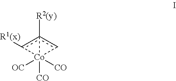
where R1 is C1-C8-alkyl, R2 is C1-C8 alkyl, x is zero, 1 or 2; and y is zero or 1.

Claims (18)
Priority Applications (6)
| Application Number | Priority Date | Filing Date | Title |
|---|---|---|---|
| US14/465,610 US9349637B2 (en) | 2014-08-21 | 2014-08-21 | Method for void-free cobalt gap fill |
| TW104127083A TWI724998B (en) | 2014-08-21 | 2015-08-20 | Method for void-free cobalt gap fill |
| JP2015162354A JP2016046532A (en) | 2014-08-21 | 2015-08-20 | Method and apparatus for void-free cobalt gap fill |
| KR1020150117358A KR20160024351A (en) | 2014-08-21 | 2015-08-20 | Method for void-free cobalt gap fill |
| CN201510518752.1A CN105390438A (en) | 2014-08-21 | 2015-08-21 | Method for void-free cobalt gap fill |
| US14/873,152 US9748137B2 (en) | 2014-08-21 | 2015-10-01 | Method for void-free cobalt gap fill |
Applications Claiming Priority (1)
| Application Number | Priority Date | Filing Date | Title |
|---|---|---|---|
| US14/465,610 US9349637B2 (en) | 2014-08-21 | 2014-08-21 | Method for void-free cobalt gap fill |
Related Child Applications (1)
| Application Number | Title | Priority Date | Filing Date |
|---|---|---|---|
| US14/873,152 Continuation-In-Part US9748137B2 (en) | 2014-08-21 | 2015-10-01 | Method for void-free cobalt gap fill |
Publications (2)
| Publication Number | Publication Date |
|---|---|
| US20160056074A1 US20160056074A1 (en) | 2016-02-25 |
| US9349637B2 true US9349637B2 (en) | 2016-05-24 |
Family
ID=55348899
Family Applications (1)
| Application Number | Title | Priority Date | Filing Date |
|---|---|---|---|
| US14/465,610 Active US9349637B2 (en) | 2014-08-21 | 2014-08-21 | Method for void-free cobalt gap fill |
Country Status (5)
| Country | Link |
|---|---|
| US (1) | US9349637B2 (en) |
| JP (1) | JP2016046532A (en) |
| KR (1) | KR20160024351A (en) |
| CN (1) | CN105390438A (en) |
| TW (1) | TWI724998B (en) |
Cited By (17)
| Publication number | Priority date | Publication date | Assignee | Title |
|---|---|---|---|---|
| US20150140233A1 (en) * | 2013-11-18 | 2015-05-21 | Applied Materials, Inc. | Methods for preferential growth of cobalt within substrate features |
| US20170114459A1 (en) * | 2015-10-23 | 2017-04-27 | Applied Materials, Inc. | Bottom-Up Gap-Fill by Surface Poisoning Treatment |
| US9653353B2 (en) | 2009-08-04 | 2017-05-16 | Novellus Systems, Inc. | Tungsten feature fill |
| US9748137B2 (en) | 2014-08-21 | 2017-08-29 | Lam Research Corporation | Method for void-free cobalt gap fill |
| US9899234B2 (en) | 2014-06-30 | 2018-02-20 | Lam Research Corporation | Liner and barrier applications for subtractive metal integration |
| US9997405B2 (en) | 2014-09-30 | 2018-06-12 | Lam Research Corporation | Feature fill with nucleation inhibition |
| US10170320B2 (en) | 2015-05-18 | 2019-01-01 | Lam Research Corporation | Feature fill with multi-stage nucleation inhibition |
| US10211099B2 (en) | 2016-12-19 | 2019-02-19 | Lam Research Corporation | Chamber conditioning for remote plasma process |
| US10242879B2 (en) | 2017-04-20 | 2019-03-26 | Lam Research Corporation | Methods and apparatus for forming smooth and conformal cobalt film by atomic layer deposition |
| US10256142B2 (en) | 2009-08-04 | 2019-04-09 | Novellus Systems, Inc. | Tungsten feature fill with nucleation inhibition |
| US10381266B2 (en) | 2012-03-27 | 2019-08-13 | Novellus Systems, Inc. | Tungsten feature fill with nucleation inhibition |
| US10418326B2 (en) | 2016-12-06 | 2019-09-17 | Samsung Electronics Co., Ltd. | Semiconductor device and method of fabricating the same |
| US10438847B2 (en) | 2016-05-13 | 2019-10-08 | Lam Research Corporation | Manganese barrier and adhesion layers for cobalt |
| US10573522B2 (en) | 2016-08-16 | 2020-02-25 | Lam Research Corporation | Method for preventing line bending during metal fill process |
| US11015241B2 (en) | 2016-06-06 | 2021-05-25 | Wayne State University | Reaction of diazadiene complexes with amines |
| US11437269B2 (en) | 2012-03-27 | 2022-09-06 | Novellus Systems, Inc. | Tungsten feature fill with nucleation inhibition |
| US11827978B2 (en) | 2019-08-23 | 2023-11-28 | Asm Ip Holding B.V. | Methods for depositing a molybdenum nitride film on a surface of a substrate by a cyclical deposition process and related semiconductor device structures including a molybdenum nitride film |
Families Citing this family (323)
| Publication number | Priority date | Publication date | Assignee | Title |
|---|---|---|---|---|
| US10378106B2 (en) | 2008-11-14 | 2019-08-13 | Asm Ip Holding B.V. | Method of forming insulation film by modified PEALD |
| US9394608B2 (en) | 2009-04-06 | 2016-07-19 | Asm America, Inc. | Semiconductor processing reactor and components thereof |
| US8802201B2 (en) | 2009-08-14 | 2014-08-12 | Asm America, Inc. | Systems and methods for thin-film deposition of metal oxides using excited nitrogen-oxygen species |
| US9312155B2 (en) | 2011-06-06 | 2016-04-12 | Asm Japan K.K. | High-throughput semiconductor-processing apparatus equipped with multiple dual-chamber modules |
| US10364496B2 (en) | 2011-06-27 | 2019-07-30 | Asm Ip Holding B.V. | Dual section module having shared and unshared mass flow controllers |
| US10854498B2 (en) | 2011-07-15 | 2020-12-01 | Asm Ip Holding B.V. | Wafer-supporting device and method for producing same |
| US20130023129A1 (en) | 2011-07-20 | 2013-01-24 | Asm America, Inc. | Pressure transmitter for a semiconductor processing environment |
| US9017481B1 (en) | 2011-10-28 | 2015-04-28 | Asm America, Inc. | Process feed management for semiconductor substrate processing |
| US9659799B2 (en) | 2012-08-28 | 2017-05-23 | Asm Ip Holding B.V. | Systems and methods for dynamic semiconductor process scheduling |
| US10714315B2 (en) | 2012-10-12 | 2020-07-14 | Asm Ip Holdings B.V. | Semiconductor reaction chamber showerhead |
| US9484191B2 (en) | 2013-03-08 | 2016-11-01 | Asm Ip Holding B.V. | Pulsed remote plasma method and system |
| US9589770B2 (en) | 2013-03-08 | 2017-03-07 | Asm Ip Holding B.V. | Method and systems for in-situ formation of intermediate reactive species |
| US9240412B2 (en) | 2013-09-27 | 2016-01-19 | Asm Ip Holding B.V. | Semiconductor structure and device and methods of forming same using selective epitaxial process |
| US10683571B2 (en) | 2014-02-25 | 2020-06-16 | Asm Ip Holding B.V. | Gas supply manifold and method of supplying gases to chamber using same |
| US10167557B2 (en) | 2014-03-18 | 2019-01-01 | Asm Ip Holding B.V. | Gas distribution system, reactor including the system, and methods of using the same |
| US11015245B2 (en) | 2014-03-19 | 2021-05-25 | Asm Ip Holding B.V. | Gas-phase reactor and system having exhaust plenum and components thereof |
| US10858737B2 (en) | 2014-07-28 | 2020-12-08 | Asm Ip Holding B.V. | Showerhead assembly and components thereof |
| US9890456B2 (en) | 2014-08-21 | 2018-02-13 | Asm Ip Holding B.V. | Method and system for in situ formation of gas-phase compounds |
| US9601430B2 (en) * | 2014-10-02 | 2017-03-21 | Taiwan Semiconductor Manufacturing Co., Ltd. | Semiconductor device structure and method for forming the same |
| US10941490B2 (en) | 2014-10-07 | 2021-03-09 | Asm Ip Holding B.V. | Multiple temperature range susceptor, assembly, reactor and system including the susceptor, and methods of using the same |
| US9657845B2 (en) | 2014-10-07 | 2017-05-23 | Asm Ip Holding B.V. | Variable conductance gas distribution apparatus and method |
| KR102263121B1 (en) | 2014-12-22 | 2021-06-09 | 에이에스엠 아이피 홀딩 비.브이. | Semiconductor device and manufacuring method thereof |
| US9576811B2 (en) | 2015-01-12 | 2017-02-21 | Lam Research Corporation | Integrating atomic scale processes: ALD (atomic layer deposition) and ALE (atomic layer etch) |
| US10529542B2 (en) | 2015-03-11 | 2020-01-07 | Asm Ip Holdings B.V. | Cross-flow reactor and method |
| US10276355B2 (en) | 2015-03-12 | 2019-04-30 | Asm Ip Holding B.V. | Multi-zone reactor, system including the reactor, and method of using the same |
| US9806252B2 (en) | 2015-04-20 | 2017-10-31 | Lam Research Corporation | Dry plasma etch method to pattern MRAM stack |
| US9870899B2 (en) | 2015-04-24 | 2018-01-16 | Lam Research Corporation | Cobalt etch back |
| US10458018B2 (en) | 2015-06-26 | 2019-10-29 | Asm Ip Holding B.V. | Structures including metal carbide material, devices including the structures, and methods of forming same |
| US10600673B2 (en) | 2015-07-07 | 2020-03-24 | Asm Ip Holding B.V. | Magnetic susceptor to baseplate seal |
| US10083836B2 (en) | 2015-07-24 | 2018-09-25 | Asm Ip Holding B.V. | Formation of boron-doped titanium metal films with high work function |
| US9960072B2 (en) | 2015-09-29 | 2018-05-01 | Asm Ip Holding B.V. | Variable adjustment for precise matching of multiple chamber cavity housings |
| US10211308B2 (en) | 2015-10-21 | 2019-02-19 | Asm Ip Holding B.V. | NbMC layers |
| US10322384B2 (en) | 2015-11-09 | 2019-06-18 | Asm Ip Holding B.V. | Counter flow mixer for process chamber |
| US11139308B2 (en) | 2015-12-29 | 2021-10-05 | Asm Ip Holding B.V. | Atomic layer deposition of III-V compounds to form V-NAND devices |
| US10727073B2 (en) | 2016-02-04 | 2020-07-28 | Lam Research Corporation | Atomic layer etching 3D structures: Si and SiGe and Ge smoothness on horizontal and vertical surfaces |
| US10229837B2 (en) | 2016-02-04 | 2019-03-12 | Lam Research Corporation | Control of directionality in atomic layer etching |
| US10468251B2 (en) | 2016-02-19 | 2019-11-05 | Asm Ip Holding B.V. | Method for forming spacers using silicon nitride film for spacer-defined multiple patterning |
| US10529554B2 (en) | 2016-02-19 | 2020-01-07 | Asm Ip Holding B.V. | Method for forming silicon nitride film selectively on sidewalls or flat surfaces of trenches |
| US10501866B2 (en) | 2016-03-09 | 2019-12-10 | Asm Ip Holding B.V. | Gas distribution apparatus for improved film uniformity in an epitaxial system |
| US10343920B2 (en) | 2016-03-18 | 2019-07-09 | Asm Ip Holding B.V. | Aligned carbon nanotubes |
| US9892913B2 (en) | 2016-03-24 | 2018-02-13 | Asm Ip Holding B.V. | Radial and thickness control via biased multi-port injection settings |
| US10190213B2 (en) | 2016-04-21 | 2019-01-29 | Asm Ip Holding B.V. | Deposition of metal borides |
| US10865475B2 (en) | 2016-04-21 | 2020-12-15 | Asm Ip Holding B.V. | Deposition of metal borides and silicides |
| US10367080B2 (en) | 2016-05-02 | 2019-07-30 | Asm Ip Holding B.V. | Method of forming a germanium oxynitride film |
| US10032628B2 (en) | 2016-05-02 | 2018-07-24 | Asm Ip Holding B.V. | Source/drain performance through conformal solid state doping |
| KR102592471B1 (en) | 2016-05-17 | 2023-10-20 | 에이에스엠 아이피 홀딩 비.브이. | Method of forming metal interconnection and method of fabricating semiconductor device using the same |
| US11453943B2 (en) | 2016-05-25 | 2022-09-27 | Asm Ip Holding B.V. | Method for forming carbon-containing silicon/metal oxide or nitride film by ALD using silicon precursor and hydrocarbon precursor |
| TWI729457B (en) | 2016-06-14 | 2021-06-01 | 美商應用材料股份有限公司 | Oxidative volumetric expansion of metals and metal containing compounds |
| US10388509B2 (en) | 2016-06-28 | 2019-08-20 | Asm Ip Holding B.V. | Formation of epitaxial layers via dislocation filtering |
| US9859151B1 (en) | 2016-07-08 | 2018-01-02 | Asm Ip Holding B.V. | Selective film deposition method to form air gaps |
| US10612137B2 (en) | 2016-07-08 | 2020-04-07 | Asm Ip Holdings B.V. | Organic reactants for atomic layer deposition |
| US10714385B2 (en) | 2016-07-19 | 2020-07-14 | Asm Ip Holding B.V. | Selective deposition of tungsten |
| US10381226B2 (en) | 2016-07-27 | 2019-08-13 | Asm Ip Holding B.V. | Method of processing substrate |
| US10395919B2 (en) | 2016-07-28 | 2019-08-27 | Asm Ip Holding B.V. | Method and apparatus for filling a gap |
| US9812320B1 (en) | 2016-07-28 | 2017-11-07 | Asm Ip Holding B.V. | Method and apparatus for filling a gap |
| KR102532607B1 (en) | 2016-07-28 | 2023-05-15 | 에이에스엠 아이피 홀딩 비.브이. | Substrate processing apparatus and method of operating the same |
| US9887082B1 (en) | 2016-07-28 | 2018-02-06 | Asm Ip Holding B.V. | Method and apparatus for filling a gap |
| US10410943B2 (en) | 2016-10-13 | 2019-09-10 | Asm Ip Holding B.V. | Method for passivating a surface of a semiconductor and related systems |
| US10643826B2 (en) | 2016-10-26 | 2020-05-05 | Asm Ip Holdings B.V. | Methods for thermally calibrating reaction chambers |
| US11532757B2 (en) | 2016-10-27 | 2022-12-20 | Asm Ip Holding B.V. | Deposition of charge trapping layers |
| US10714350B2 (en) | 2016-11-01 | 2020-07-14 | ASM IP Holdings, B.V. | Methods for forming a transition metal niobium nitride film on a substrate by atomic layer deposition and related semiconductor device structures |
| US10643904B2 (en) | 2016-11-01 | 2020-05-05 | Asm Ip Holdings B.V. | Methods for forming a semiconductor device and related semiconductor device structures |
| US10229833B2 (en) | 2016-11-01 | 2019-03-12 | Asm Ip Holding B.V. | Methods for forming a transition metal nitride film on a substrate by atomic layer deposition and related semiconductor device structures |
| US10435790B2 (en) | 2016-11-01 | 2019-10-08 | Asm Ip Holding B.V. | Method of subatmospheric plasma-enhanced ALD using capacitively coupled electrodes with narrow gap |
| TWI719262B (en) | 2016-11-03 | 2021-02-21 | 美商應用材料股份有限公司 | Deposition and treatment of films for patterning |
| US10134757B2 (en) | 2016-11-07 | 2018-11-20 | Asm Ip Holding B.V. | Method of processing a substrate and a device manufactured by using the method |
| CN109923662A (en) | 2016-11-08 | 2019-06-21 | 应用材料公司 | For patterning the geometry control of the bottom-up column of application |
| KR102546317B1 (en) | 2016-11-15 | 2023-06-21 | 에이에스엠 아이피 홀딩 비.브이. | Gas supply unit and substrate processing apparatus including the same |
| US10340135B2 (en) | 2016-11-28 | 2019-07-02 | Asm Ip Holding B.V. | Method of topologically restricted plasma-enhanced cyclic deposition of silicon or metal nitride |
| KR20180068582A (en) | 2016-12-14 | 2018-06-22 | 에이에스엠 아이피 홀딩 비.브이. | Substrate processing apparatus |
| US11581186B2 (en) | 2016-12-15 | 2023-02-14 | Asm Ip Holding B.V. | Sequential infiltration synthesis apparatus |
| US11289374B2 (en) * | 2016-12-15 | 2022-03-29 | Applied Materials, Inc. | Nucleation-free gap fill ALD process |
| US11447861B2 (en) | 2016-12-15 | 2022-09-20 | Asm Ip Holding B.V. | Sequential infiltration synthesis apparatus and a method of forming a patterned structure |
| KR20180070971A (en) | 2016-12-19 | 2018-06-27 | 에이에스엠 아이피 홀딩 비.브이. | Substrate processing apparatus |
| US10269558B2 (en) | 2016-12-22 | 2019-04-23 | Asm Ip Holding B.V. | Method of forming a structure on a substrate |
| US10867788B2 (en) | 2016-12-28 | 2020-12-15 | Asm Ip Holding B.V. | Method of forming a structure on a substrate |
| TWI758398B (en) * | 2017-01-24 | 2022-03-21 | 美商應用材料股份有限公司 | Method of forming cobalt layer on substrate |
| US10655221B2 (en) | 2017-02-09 | 2020-05-19 | Asm Ip Holding B.V. | Method for depositing oxide film by thermal ALD and PEALD |
| US10176984B2 (en) | 2017-02-14 | 2019-01-08 | Lam Research Corporation | Selective deposition of silicon oxide |
| US10468261B2 (en) | 2017-02-15 | 2019-11-05 | Asm Ip Holding B.V. | Methods for forming a metallic film on a substrate by cyclical deposition and related semiconductor device structures |
| US10770349B2 (en) | 2017-02-22 | 2020-09-08 | Applied Materials, Inc. | Critical dimension control for self-aligned contact patterning |
| KR102553120B1 (en) * | 2017-03-07 | 2023-07-06 | 도쿄엘렉트론가부시키가이샤 | Method of filling retrograde recessed features |
| US10242866B2 (en) | 2017-03-08 | 2019-03-26 | Lam Research Corporation | Selective deposition of silicon nitride on silicon oxide using catalytic control |
| US10103056B2 (en) * | 2017-03-08 | 2018-10-16 | Lam Research Corporation | Methods for wet metal seed deposition for bottom up gapfill of features |
| US9911595B1 (en) | 2017-03-17 | 2018-03-06 | Lam Research Corporation | Selective growth of silicon nitride |
| US10283353B2 (en) | 2017-03-29 | 2019-05-07 | Asm Ip Holding B.V. | Method of reforming insulating film deposited on substrate with recess pattern |
| US10529563B2 (en) | 2017-03-29 | 2020-01-07 | Asm Ip Holdings B.V. | Method for forming doped metal oxide films on a substrate by cyclical deposition and related semiconductor device structures |
| JP7113651B2 (en) * | 2017-04-11 | 2022-08-05 | 東京エレクトロン株式会社 | Void-free filling method for recessed features with retrograde profiles |
| US10559461B2 (en) * | 2017-04-19 | 2020-02-11 | Lam Research Corporation | Selective deposition with atomic layer etch reset |
| US10832909B2 (en) | 2017-04-24 | 2020-11-10 | Lam Research Corporation | Atomic layer etch, reactive precursors and energetic sources for patterning applications |
| WO2018200212A1 (en) * | 2017-04-25 | 2018-11-01 | Applied Materials, Inc. | Selective deposition of tungsten for simplified process flow of tungsten oxide pillar formation |
| KR102457289B1 (en) | 2017-04-25 | 2022-10-21 | 에이에스엠 아이피 홀딩 비.브이. | Method for depositing a thin film and manufacturing a semiconductor device |
| US10446393B2 (en) | 2017-05-08 | 2019-10-15 | Asm Ip Holding B.V. | Methods for forming silicon-containing epitaxial layers and related semiconductor device structures |
| US10892156B2 (en) | 2017-05-08 | 2021-01-12 | Asm Ip Holding B.V. | Methods for forming a silicon nitride film on a substrate and related semiconductor device structures |
| US10770286B2 (en) | 2017-05-08 | 2020-09-08 | Asm Ip Holdings B.V. | Methods for selectively forming a silicon nitride film on a substrate and related semiconductor device structures |
| US10504742B2 (en) | 2017-05-31 | 2019-12-10 | Asm Ip Holding B.V. | Method of atomic layer etching using hydrogen plasma |
| US10886123B2 (en) | 2017-06-02 | 2021-01-05 | Asm Ip Holding B.V. | Methods for forming low temperature semiconductor layers and related semiconductor device structures |
| US10840186B2 (en) | 2017-06-10 | 2020-11-17 | Applied Materials, Inc. | Methods of forming self-aligned vias and air gaps |
| CN111032908B (en) | 2017-06-23 | 2024-01-30 | 默克专利有限公司 | Atomic layer deposition method for selective film growth |
| TW201906035A (en) | 2017-06-24 | 2019-02-01 | 美商微材料有限責任公司 | Method of producing fully self-aligned vias and contacts |
| US11306395B2 (en) | 2017-06-28 | 2022-04-19 | Asm Ip Holding B.V. | Methods for depositing a transition metal nitride film on a substrate by atomic layer deposition and related deposition apparatus |
| US10685834B2 (en) | 2017-07-05 | 2020-06-16 | Asm Ip Holdings B.V. | Methods for forming a silicon germanium tin layer and related semiconductor device structures |
| KR20190009245A (en) | 2017-07-18 | 2019-01-28 | 에이에스엠 아이피 홀딩 비.브이. | Methods for forming a semiconductor device structure and related semiconductor device structures |
| US11374112B2 (en) | 2017-07-19 | 2022-06-28 | Asm Ip Holding B.V. | Method for depositing a group IV semiconductor and related semiconductor device structures |
| US10541333B2 (en) | 2017-07-19 | 2020-01-21 | Asm Ip Holding B.V. | Method for depositing a group IV semiconductor and related semiconductor device structures |
| US11018002B2 (en) | 2017-07-19 | 2021-05-25 | Asm Ip Holding B.V. | Method for selectively depositing a Group IV semiconductor and related semiconductor device structures |
| US10605530B2 (en) | 2017-07-26 | 2020-03-31 | Asm Ip Holding B.V. | Assembly of a liner and a flange for a vertical furnace as well as the liner and the vertical furnace |
| US10312055B2 (en) | 2017-07-26 | 2019-06-04 | Asm Ip Holding B.V. | Method of depositing film by PEALD using negative bias |
| US10590535B2 (en) | 2017-07-26 | 2020-03-17 | Asm Ip Holdings B.V. | Chemical treatment, deposition and/or infiltration apparatus and method for using the same |
| US10770336B2 (en) | 2017-08-08 | 2020-09-08 | Asm Ip Holding B.V. | Substrate lift mechanism and reactor including same |
| US10692741B2 (en) | 2017-08-08 | 2020-06-23 | Asm Ip Holdings B.V. | Radiation shield |
| US11139191B2 (en) | 2017-08-09 | 2021-10-05 | Asm Ip Holding B.V. | Storage apparatus for storing cassettes for substrates and processing apparatus equipped therewith |
| US11769682B2 (en) | 2017-08-09 | 2023-09-26 | Asm Ip Holding B.V. | Storage apparatus for storing cassettes for substrates and processing apparatus equipped therewith |
| US10249524B2 (en) | 2017-08-09 | 2019-04-02 | Asm Ip Holding B.V. | Cassette holder assembly for a substrate cassette and holding member for use in such assembly |
| USD900036S1 (en) | 2017-08-24 | 2020-10-27 | Asm Ip Holding B.V. | Heater electrical connector and adapter |
| US11830730B2 (en) | 2017-08-29 | 2023-11-28 | Asm Ip Holding B.V. | Layer forming method and apparatus |
| KR102491945B1 (en) | 2017-08-30 | 2023-01-26 | 에이에스엠 아이피 홀딩 비.브이. | Substrate processing apparatus |
| US11295980B2 (en) | 2017-08-30 | 2022-04-05 | Asm Ip Holding B.V. | Methods for depositing a molybdenum metal film over a dielectric surface of a substrate by a cyclical deposition process and related semiconductor device structures |
| US11056344B2 (en) | 2017-08-30 | 2021-07-06 | Asm Ip Holding B.V. | Layer forming method |
| WO2019046399A1 (en) | 2017-08-31 | 2019-03-07 | Micromaterials Llc | Methods of producing self-aligned vias |
| WO2019046402A1 (en) | 2017-08-31 | 2019-03-07 | Micromaterials Llc | Methods of producing self-aligned grown via |
| WO2019050735A1 (en) | 2017-09-06 | 2019-03-14 | Micromaterials Llc | Methods of producing self-aligned vias |
| US10607895B2 (en) | 2017-09-18 | 2020-03-31 | Asm Ip Holdings B.V. | Method for forming a semiconductor device structure comprising a gate fill metal |
| US10304732B2 (en) * | 2017-09-21 | 2019-05-28 | Applied Materials, Inc. | Methods and apparatus for filling substrate features with cobalt |
| KR102630301B1 (en) | 2017-09-21 | 2024-01-29 | 에이에스엠 아이피 홀딩 비.브이. | Method of sequential infiltration synthesis treatment of infiltrateable material and structures and devices formed using same |
| US10844484B2 (en) | 2017-09-22 | 2020-11-24 | Asm Ip Holding B.V. | Apparatus for dispensing a vapor phase reactant to a reaction chamber and related methods |
| US10658205B2 (en) | 2017-09-28 | 2020-05-19 | Asm Ip Holdings B.V. | Chemical dispensing apparatus and methods for dispensing a chemical to a reaction chamber |
| US10403504B2 (en) | 2017-10-05 | 2019-09-03 | Asm Ip Holding B.V. | Method for selectively depositing a metallic film on a substrate |
| US10319588B2 (en) | 2017-10-10 | 2019-06-11 | Asm Ip Holding B.V. | Method for depositing a metal chalcogenide on a substrate by cyclical deposition |
| US10923344B2 (en) | 2017-10-30 | 2021-02-16 | Asm Ip Holding B.V. | Methods for forming a semiconductor structure and related semiconductor structures |
| US10910262B2 (en) | 2017-11-16 | 2021-02-02 | Asm Ip Holding B.V. | Method of selectively depositing a capping layer structure on a semiconductor device structure |
| KR102443047B1 (en) | 2017-11-16 | 2022-09-14 | 에이에스엠 아이피 홀딩 비.브이. | Method of processing a substrate and a device manufactured by the same |
| US10460930B2 (en) | 2017-11-22 | 2019-10-29 | Lam Research Corporation | Selective growth of SiO2 on dielectric surfaces in the presence of copper |
| US11022879B2 (en) | 2017-11-24 | 2021-06-01 | Asm Ip Holding B.V. | Method of forming an enhanced unexposed photoresist layer |
| JP7214724B2 (en) | 2017-11-27 | 2023-01-30 | エーエスエム アイピー ホールディング ビー.ブイ. | Storage device for storing wafer cassettes used in batch furnaces |
| TWI791689B (en) | 2017-11-27 | 2023-02-11 | 荷蘭商Asm智慧財產控股私人有限公司 | Apparatus including a clean mini environment |
| US10290508B1 (en) | 2017-12-05 | 2019-05-14 | Asm Ip Holding B.V. | Method for forming vertical spacers for spacer-defined patterning |
| CN110034017A (en) | 2017-12-07 | 2019-07-19 | 微材料有限责任公司 | Method for making metal and barrier layer-liner controllably be recessed |
| EP3499557A1 (en) | 2017-12-15 | 2019-06-19 | Micromaterials LLC | Selectively etched self-aligned via processes |
| US10872771B2 (en) | 2018-01-16 | 2020-12-22 | Asm Ip Holding B. V. | Method for depositing a material film on a substrate within a reaction chamber by a cyclical deposition process and related device structures |
| WO2019142055A2 (en) | 2018-01-19 | 2019-07-25 | Asm Ip Holding B.V. | Method for depositing a gap-fill layer by plasma-assisted deposition |
| TWI799494B (en) | 2018-01-19 | 2023-04-21 | 荷蘭商Asm 智慧財產控股公司 | Deposition method |
| USD903477S1 (en) | 2018-01-24 | 2020-12-01 | Asm Ip Holdings B.V. | Metal clamp |
| US11018047B2 (en) | 2018-01-25 | 2021-05-25 | Asm Ip Holding B.V. | Hybrid lift pin |
| US10535516B2 (en) | 2018-02-01 | 2020-01-14 | Asm Ip Holdings B.V. | Method for depositing a semiconductor structure on a surface of a substrate and related semiconductor structures |
| USD880437S1 (en) | 2018-02-01 | 2020-04-07 | Asm Ip Holding B.V. | Gas supply plate for semiconductor manufacturing apparatus |
| US11081345B2 (en) | 2018-02-06 | 2021-08-03 | Asm Ip Holding B.V. | Method of post-deposition treatment for silicon oxide film |
| US10896820B2 (en) | 2018-02-14 | 2021-01-19 | Asm Ip Holding B.V. | Method for depositing a ruthenium-containing film on a substrate by a cyclical deposition process |
| US11685991B2 (en) | 2018-02-14 | 2023-06-27 | Asm Ip Holding B.V. | Method for depositing a ruthenium-containing film on a substrate by a cyclical deposition process |
| US10731249B2 (en) | 2018-02-15 | 2020-08-04 | Asm Ip Holding B.V. | Method of forming a transition metal containing film on a substrate by a cyclical deposition process, a method for supplying a transition metal halide compound to a reaction chamber, and related vapor deposition apparatus |
| US10658181B2 (en) | 2018-02-20 | 2020-05-19 | Asm Ip Holding B.V. | Method of spacer-defined direct patterning in semiconductor fabrication |
| KR102636427B1 (en) | 2018-02-20 | 2024-02-13 | 에이에스엠 아이피 홀딩 비.브이. | Substrate processing method and apparatus |
| US10975470B2 (en) | 2018-02-23 | 2021-04-13 | Asm Ip Holding B.V. | Apparatus for detecting or monitoring for a chemical precursor in a high temperature environment |
| US11473195B2 (en) | 2018-03-01 | 2022-10-18 | Asm Ip Holding B.V. | Semiconductor processing apparatus and a method for processing a substrate |
| KR20200118504A (en) | 2018-03-02 | 2020-10-15 | 램 리써치 코포레이션 | Selective deposition using hydrolysis |
| KR20190104902A (en) | 2018-03-02 | 2019-09-11 | 마이크로머티어리얼즈 엘엘씨 | Methods for removing metal oxides |
| US11629406B2 (en) | 2018-03-09 | 2023-04-18 | Asm Ip Holding B.V. | Semiconductor processing apparatus comprising one or more pyrometers for measuring a temperature of a substrate during transfer of the substrate |
| US11114283B2 (en) | 2018-03-16 | 2021-09-07 | Asm Ip Holding B.V. | Reactor, system including the reactor, and methods of manufacturing and using same |
| KR102646467B1 (en) | 2018-03-27 | 2024-03-11 | 에이에스엠 아이피 홀딩 비.브이. | Method of forming an electrode on a substrate and a semiconductor device structure including an electrode |
| US11230766B2 (en) | 2018-03-29 | 2022-01-25 | Asm Ip Holding B.V. | Substrate processing apparatus and method |
| US10510536B2 (en) | 2018-03-29 | 2019-12-17 | Asm Ip Holding B.V. | Method of depositing a co-doped polysilicon film on a surface of a substrate within a reaction chamber |
| US11088002B2 (en) | 2018-03-29 | 2021-08-10 | Asm Ip Holding B.V. | Substrate rack and a substrate processing system and method |
| KR102501472B1 (en) | 2018-03-30 | 2023-02-20 | 에이에스엠 아이피 홀딩 비.브이. | Substrate processing method |
| KR20200141522A (en) | 2018-05-04 | 2020-12-18 | 어플라이드 머티어리얼스, 인코포레이티드 | Deposition of metal films |
| TW202002219A (en) | 2018-05-08 | 2020-01-01 | 美商微材料有限責任公司 | Selective removal process to create high aspect ratio fully self-aligned via |
| TWI811348B (en) | 2018-05-08 | 2023-08-11 | 荷蘭商Asm 智慧財產控股公司 | Methods for depositing an oxide film on a substrate by a cyclical deposition process and related device structures |
| KR20190129718A (en) | 2018-05-11 | 2019-11-20 | 에이에스엠 아이피 홀딩 비.브이. | Methods for forming a doped metal carbide film on a substrate and related semiconductor device structures |
| TW202011547A (en) | 2018-05-16 | 2020-03-16 | 美商微材料有限責任公司 | A method for creating a fully self-aligned via |
| KR102596988B1 (en) | 2018-05-28 | 2023-10-31 | 에이에스엠 아이피 홀딩 비.브이. | Method of processing a substrate and a device manufactured by the same |
| TWI740046B (en) | 2018-05-28 | 2021-09-21 | 國立清華大學 | Atomic layer deposition and cobalt metal film |
| US11718913B2 (en) | 2018-06-04 | 2023-08-08 | Asm Ip Holding B.V. | Gas distribution system and reactor system including same |
| TW202013553A (en) | 2018-06-04 | 2020-04-01 | 荷蘭商Asm 智慧財產控股公司 | Wafer handling chamber with moisture reduction |
| US11286562B2 (en) | 2018-06-08 | 2022-03-29 | Asm Ip Holding B.V. | Gas-phase chemical reactor and method of using same |
| WO2019236350A1 (en) | 2018-06-08 | 2019-12-12 | Micromaterials Llc | A method for creating a fully self-aligned via |
| KR102568797B1 (en) | 2018-06-21 | 2023-08-21 | 에이에스엠 아이피 홀딩 비.브이. | Substrate processing system |
| US10797133B2 (en) | 2018-06-21 | 2020-10-06 | Asm Ip Holding B.V. | Method for depositing a phosphorus doped silicon arsenide film and related semiconductor device structures |
| CN112292478A (en) | 2018-06-27 | 2021-01-29 | Asm Ip私人控股有限公司 | Cyclic deposition methods for forming metal-containing materials and films and structures containing metal-containing materials |
| JP2021529880A (en) | 2018-06-27 | 2021-11-04 | エーエスエム・アイピー・ホールディング・ベー・フェー | Periodic deposition methods for forming metal-containing materials and films and structures containing metal-containing materials |
| KR20200002519A (en) | 2018-06-29 | 2020-01-08 | 에이에스엠 아이피 홀딩 비.브이. | Method for depositing a thin film and manufacturing a semiconductor device |
| US10612136B2 (en) | 2018-06-29 | 2020-04-07 | ASM IP Holding, B.V. | Temperature-controlled flange and reactor system including same |
| US10388513B1 (en) | 2018-07-03 | 2019-08-20 | Asm Ip Holding B.V. | Method for depositing silicon-free carbon-containing film as gap-fill layer by pulse plasma-assisted deposition |
| US10755922B2 (en) | 2018-07-03 | 2020-08-25 | Asm Ip Holding B.V. | Method for depositing silicon-free carbon-containing film as gap-fill layer by pulse plasma-assisted deposition |
| US10767789B2 (en) | 2018-07-16 | 2020-09-08 | Asm Ip Holding B.V. | Diaphragm valves, valve components, and methods for forming valve components |
| US10483099B1 (en) | 2018-07-26 | 2019-11-19 | Asm Ip Holding B.V. | Method for forming thermally stable organosilicon polymer film |
| US11053591B2 (en) | 2018-08-06 | 2021-07-06 | Asm Ip Holding B.V. | Multi-port gas injection system and reactor system including same |
| US10883175B2 (en) | 2018-08-09 | 2021-01-05 | Asm Ip Holding B.V. | Vertical furnace for processing substrates and a liner for use therein |
| US10829852B2 (en) | 2018-08-16 | 2020-11-10 | Asm Ip Holding B.V. | Gas distribution device for a wafer processing apparatus |
| US11430674B2 (en) | 2018-08-22 | 2022-08-30 | Asm Ip Holding B.V. | Sensor array, apparatus for dispensing a vapor phase reactant to a reaction chamber and related methods |
| KR20200030162A (en) | 2018-09-11 | 2020-03-20 | 에이에스엠 아이피 홀딩 비.브이. | Method for deposition of a thin film |
| US11024523B2 (en) | 2018-09-11 | 2021-06-01 | Asm Ip Holding B.V. | Substrate processing apparatus and method |
| US11049751B2 (en) | 2018-09-14 | 2021-06-29 | Asm Ip Holding B.V. | Cassette supply system to store and handle cassettes and processing apparatus equipped therewith |
| CN110970344A (en) | 2018-10-01 | 2020-04-07 | Asm Ip控股有限公司 | Substrate holding apparatus, system including the same, and method of using the same |
| US11232963B2 (en) | 2018-10-03 | 2022-01-25 | Asm Ip Holding B.V. | Substrate processing apparatus and method |
| KR102592699B1 (en) | 2018-10-08 | 2023-10-23 | 에이에스엠 아이피 홀딩 비.브이. | Substrate support unit and apparatuses for depositing thin film and processing the substrate including the same |
| US10847365B2 (en) | 2018-10-11 | 2020-11-24 | Asm Ip Holding B.V. | Method of forming conformal silicon carbide film by cyclic CVD |
| US10811256B2 (en) | 2018-10-16 | 2020-10-20 | Asm Ip Holding B.V. | Method for etching a carbon-containing feature |
| KR102546322B1 (en) | 2018-10-19 | 2023-06-21 | 에이에스엠 아이피 홀딩 비.브이. | Substrate processing apparatus and substrate processing method |
| KR102605121B1 (en) | 2018-10-19 | 2023-11-23 | 에이에스엠 아이피 홀딩 비.브이. | Substrate processing apparatus and substrate processing method |
| USD948463S1 (en) | 2018-10-24 | 2022-04-12 | Asm Ip Holding B.V. | Susceptor for semiconductor substrate supporting apparatus |
| US10381219B1 (en) | 2018-10-25 | 2019-08-13 | Asm Ip Holding B.V. | Methods for forming a silicon nitride film |
| US11087997B2 (en) | 2018-10-31 | 2021-08-10 | Asm Ip Holding B.V. | Substrate processing apparatus for processing substrates |
| KR20200051105A (en) | 2018-11-02 | 2020-05-13 | 에이에스엠 아이피 홀딩 비.브이. | Substrate support unit and substrate processing apparatus including the same |
| US11572620B2 (en) | 2018-11-06 | 2023-02-07 | Asm Ip Holding B.V. | Methods for selectively depositing an amorphous silicon film on a substrate |
| US11031242B2 (en) | 2018-11-07 | 2021-06-08 | Asm Ip Holding B.V. | Methods for depositing a boron doped silicon germanium film |
| US10818758B2 (en) | 2018-11-16 | 2020-10-27 | Asm Ip Holding B.V. | Methods for forming a metal silicate film on a substrate in a reaction chamber and related semiconductor device structures |
| US10847366B2 (en) | 2018-11-16 | 2020-11-24 | Asm Ip Holding B.V. | Methods for depositing a transition metal chalcogenide film on a substrate by a cyclical deposition process |
| US10559458B1 (en) | 2018-11-26 | 2020-02-11 | Asm Ip Holding B.V. | Method of forming oxynitride film |
| US11217444B2 (en) | 2018-11-30 | 2022-01-04 | Asm Ip Holding B.V. | Method for forming an ultraviolet radiation responsive metal oxide-containing film |
| KR102636428B1 (en) | 2018-12-04 | 2024-02-13 | 에이에스엠 아이피 홀딩 비.브이. | A method for cleaning a substrate processing apparatus |
| US11158513B2 (en) | 2018-12-13 | 2021-10-26 | Asm Ip Holding B.V. | Methods for forming a rhenium-containing film on a substrate by a cyclical deposition process and related semiconductor device structures |
| TW202037745A (en) | 2018-12-14 | 2020-10-16 | 荷蘭商Asm Ip私人控股有限公司 | Method of forming device structure, structure formed by the method and system for performing the method |
| TWI819180B (en) | 2019-01-17 | 2023-10-21 | 荷蘭商Asm 智慧財產控股公司 | Methods of forming a transition metal containing film on a substrate by a cyclical deposition process |
| KR20200091543A (en) | 2019-01-22 | 2020-07-31 | 에이에스엠 아이피 홀딩 비.브이. | Semiconductor processing device |
| CN111524788B (en) | 2019-02-01 | 2023-11-24 | Asm Ip私人控股有限公司 | Method for topologically selective film formation of silicon oxide |
| KR102626263B1 (en) | 2019-02-20 | 2024-01-16 | 에이에스엠 아이피 홀딩 비.브이. | Cyclical deposition method including treatment step and apparatus for same |
| KR20200102357A (en) | 2019-02-20 | 2020-08-31 | 에이에스엠 아이피 홀딩 비.브이. | Apparatus and methods for plug fill deposition in 3-d nand applications |
| JP2020136678A (en) | 2019-02-20 | 2020-08-31 | エーエスエム・アイピー・ホールディング・ベー・フェー | Method for filing concave part formed inside front surface of base material, and device |
| JP2020136677A (en) | 2019-02-20 | 2020-08-31 | エーエスエム・アイピー・ホールディング・ベー・フェー | Periodic accumulation method for filing concave part formed inside front surface of base material, and device |
| TW202100794A (en) | 2019-02-22 | 2021-01-01 | 荷蘭商Asm Ip私人控股有限公司 | Substrate processing apparatus and method for processing substrate |
| US11742198B2 (en) | 2019-03-08 | 2023-08-29 | Asm Ip Holding B.V. | Structure including SiOCN layer and method of forming same |
| KR20200108242A (en) | 2019-03-08 | 2020-09-17 | 에이에스엠 아이피 홀딩 비.브이. | Method for Selective Deposition of Silicon Nitride Layer and Structure Including Selectively-Deposited Silicon Nitride Layer |
| KR20200108243A (en) | 2019-03-08 | 2020-09-17 | 에이에스엠 아이피 홀딩 비.브이. | Structure Including SiOC Layer and Method of Forming Same |
| US11164938B2 (en) | 2019-03-26 | 2021-11-02 | Micromaterials Llc | DRAM capacitor module |
| JP2020167398A (en) | 2019-03-28 | 2020-10-08 | エーエスエム・アイピー・ホールディング・ベー・フェー | Door opener and substrate processing apparatus provided therewith |
| KR20200116855A (en) | 2019-04-01 | 2020-10-13 | 에이에스엠 아이피 홀딩 비.브이. | Method of manufacturing semiconductor device |
| US11447864B2 (en) | 2019-04-19 | 2022-09-20 | Asm Ip Holding B.V. | Layer forming method and apparatus |
| KR20200125453A (en) | 2019-04-24 | 2020-11-04 | 에이에스엠 아이피 홀딩 비.브이. | Gas-phase reactor system and method of using same |
| KR20200130118A (en) | 2019-05-07 | 2020-11-18 | 에이에스엠 아이피 홀딩 비.브이. | Method for Reforming Amorphous Carbon Polymer Film |
| KR20200130121A (en) | 2019-05-07 | 2020-11-18 | 에이에스엠 아이피 홀딩 비.브이. | Chemical source vessel with dip tube |
| KR20200130652A (en) | 2019-05-10 | 2020-11-19 | 에이에스엠 아이피 홀딩 비.브이. | Method of depositing material onto a surface and structure formed according to the method |
| JP2020188255A (en) | 2019-05-16 | 2020-11-19 | エーエスエム アイピー ホールディング ビー.ブイ. | Wafer boat handling device, vertical batch furnace, and method |
| USD975665S1 (en) | 2019-05-17 | 2023-01-17 | Asm Ip Holding B.V. | Susceptor shaft |
| USD947913S1 (en) | 2019-05-17 | 2022-04-05 | Asm Ip Holding B.V. | Susceptor shaft |
| USD935572S1 (en) | 2019-05-24 | 2021-11-09 | Asm Ip Holding B.V. | Gas channel plate |
| USD922229S1 (en) | 2019-06-05 | 2021-06-15 | Asm Ip Holding B.V. | Device for controlling a temperature of a gas supply unit |
| KR20200141003A (en) | 2019-06-06 | 2020-12-17 | 에이에스엠 아이피 홀딩 비.브이. | Gas-phase reactor system including a gas detector |
| KR20200143254A (en) | 2019-06-11 | 2020-12-23 | 에이에스엠 아이피 홀딩 비.브이. | Method of forming an electronic structure using an reforming gas, system for performing the method, and structure formed using the method |
| USD944946S1 (en) | 2019-06-14 | 2022-03-01 | Asm Ip Holding B.V. | Shower plate |
| USD931978S1 (en) | 2019-06-27 | 2021-09-28 | Asm Ip Holding B.V. | Showerhead vacuum transport |
| CN110265353B (en) * | 2019-06-28 | 2021-06-04 | 芯盟科技有限公司 | Trench isolation structure and forming method thereof |
| KR20210005515A (en) | 2019-07-03 | 2021-01-14 | 에이에스엠 아이피 홀딩 비.브이. | Temperature control assembly for substrate processing apparatus and method of using same |
| JP2021015791A (en) | 2019-07-09 | 2021-02-12 | エーエスエム アイピー ホールディング ビー.ブイ. | Plasma device and substrate processing method using coaxial waveguide |
| CN112216646A (en) | 2019-07-10 | 2021-01-12 | Asm Ip私人控股有限公司 | Substrate supporting assembly and substrate processing device comprising same |
| KR20210010307A (en) | 2019-07-16 | 2021-01-27 | 에이에스엠 아이피 홀딩 비.브이. | Substrate processing apparatus |
| KR20210010820A (en) | 2019-07-17 | 2021-01-28 | 에이에스엠 아이피 홀딩 비.브이. | Methods of forming silicon germanium structures |
| KR20210010816A (en) | 2019-07-17 | 2021-01-28 | 에이에스엠 아이피 홀딩 비.브이. | Radical assist ignition plasma system and method |
| US11643724B2 (en) | 2019-07-18 | 2023-05-09 | Asm Ip Holding B.V. | Method of forming structures using a neutral beam |
| TW202121506A (en) | 2019-07-19 | 2021-06-01 | 荷蘭商Asm Ip私人控股有限公司 | Method of forming topology-controlled amorphous carbon polymer film |
| TW202113936A (en) | 2019-07-29 | 2021-04-01 | 荷蘭商Asm Ip私人控股有限公司 | Methods for selective deposition utilizing n-type dopants and/or alternative dopants to achieve high dopant incorporation |
| CN112309899A (en) | 2019-07-30 | 2021-02-02 | Asm Ip私人控股有限公司 | Substrate processing apparatus |
| CN112309900A (en) | 2019-07-30 | 2021-02-02 | Asm Ip私人控股有限公司 | Substrate processing apparatus |
| US11587814B2 (en) | 2019-07-31 | 2023-02-21 | Asm Ip Holding B.V. | Vertical batch furnace assembly |
| US11587815B2 (en) | 2019-07-31 | 2023-02-21 | Asm Ip Holding B.V. | Vertical batch furnace assembly |
| US11227782B2 (en) | 2019-07-31 | 2022-01-18 | Asm Ip Holding B.V. | Vertical batch furnace assembly |
| CN112323048B (en) | 2019-08-05 | 2024-02-09 | Asm Ip私人控股有限公司 | Liquid level sensor for chemical source container |
| USD965524S1 (en) | 2019-08-19 | 2022-10-04 | Asm Ip Holding B.V. | Susceptor support |
| USD965044S1 (en) | 2019-08-19 | 2022-09-27 | Asm Ip Holding B.V. | Susceptor shaft |
| JP2021031769A (en) | 2019-08-21 | 2021-03-01 | エーエスエム アイピー ホールディング ビー.ブイ. | Production apparatus of mixed gas of film deposition raw material and film deposition apparatus |
| USD930782S1 (en) | 2019-08-22 | 2021-09-14 | Asm Ip Holding B.V. | Gas distributor |
| KR20210024423A (en) | 2019-08-22 | 2021-03-05 | 에이에스엠 아이피 홀딩 비.브이. | Method for forming a structure with a hole |
| USD940837S1 (en) | 2019-08-22 | 2022-01-11 | Asm Ip Holding B.V. | Electrode |
| USD949319S1 (en) | 2019-08-22 | 2022-04-19 | Asm Ip Holding B.V. | Exhaust duct |
| USD979506S1 (en) | 2019-08-22 | 2023-02-28 | Asm Ip Holding B.V. | Insulator |
| KR20210024420A (en) | 2019-08-23 | 2021-03-05 | 에이에스엠 아이피 홀딩 비.브이. | Method for depositing silicon oxide film having improved quality by peald using bis(diethylamino)silane |
| KR20210029090A (en) | 2019-09-04 | 2021-03-15 | 에이에스엠 아이피 홀딩 비.브이. | Methods for selective deposition using a sacrificial capping layer |
| KR20210029663A (en) | 2019-09-05 | 2021-03-16 | 에이에스엠 아이피 홀딩 비.브이. | Substrate processing apparatus |
| US11562901B2 (en) | 2019-09-25 | 2023-01-24 | Asm Ip Holding B.V. | Substrate processing method |
| CN112593212B (en) | 2019-10-02 | 2023-12-22 | Asm Ip私人控股有限公司 | Method for forming topologically selective silicon oxide film by cyclic plasma enhanced deposition process |
| TW202129060A (en) | 2019-10-08 | 2021-08-01 | 荷蘭商Asm Ip控股公司 | Substrate processing device, and substrate processing method |
| KR20210043460A (en) | 2019-10-10 | 2021-04-21 | 에이에스엠 아이피 홀딩 비.브이. | Method of forming a photoresist underlayer and structure including same |
| KR20210045930A (en) | 2019-10-16 | 2021-04-27 | 에이에스엠 아이피 홀딩 비.브이. | Method of Topology-Selective Film Formation of Silicon Oxide |
| US11637014B2 (en) | 2019-10-17 | 2023-04-25 | Asm Ip Holding B.V. | Methods for selective deposition of doped semiconductor material |
| CN110797300A (en) * | 2019-10-21 | 2020-02-14 | 长江存储科技有限责任公司 | Filling method of metal tungsten |
| KR20210047808A (en) | 2019-10-21 | 2021-04-30 | 에이에스엠 아이피 홀딩 비.브이. | Apparatus and methods for selectively etching films |
| US11646205B2 (en) | 2019-10-29 | 2023-05-09 | Asm Ip Holding B.V. | Methods of selectively forming n-type doped material on a surface, systems for selectively forming n-type doped material, and structures formed using same |
| KR20210054983A (en) | 2019-11-05 | 2021-05-14 | 에이에스엠 아이피 홀딩 비.브이. | Structures with doped semiconductor layers and methods and systems for forming same |
| US11501968B2 (en) | 2019-11-15 | 2022-11-15 | Asm Ip Holding B.V. | Method for providing a semiconductor device with silicon filled gaps |
| KR20210062561A (en) | 2019-11-20 | 2021-05-31 | 에이에스엠 아이피 홀딩 비.브이. | Method of depositing carbon-containing material on a surface of a substrate, structure formed using the method, and system for forming the structure |
| CN112951697A (en) | 2019-11-26 | 2021-06-11 | Asm Ip私人控股有限公司 | Substrate processing apparatus |
| KR20210065848A (en) | 2019-11-26 | 2021-06-04 | 에이에스엠 아이피 홀딩 비.브이. | Methods for selectivley forming a target film on a substrate comprising a first dielectric surface and a second metallic surface |
| CN112885692A (en) | 2019-11-29 | 2021-06-01 | Asm Ip私人控股有限公司 | Substrate processing apparatus |
| CN112885693A (en) | 2019-11-29 | 2021-06-01 | Asm Ip私人控股有限公司 | Substrate processing apparatus |
| JP2021090042A (en) | 2019-12-02 | 2021-06-10 | エーエスエム アイピー ホールディング ビー.ブイ. | Substrate processing apparatus and substrate processing method |
| KR20210070898A (en) | 2019-12-04 | 2021-06-15 | 에이에스엠 아이피 홀딩 비.브이. | Substrate processing apparatus |
| JP2021097227A (en) | 2019-12-17 | 2021-06-24 | エーエスエム・アイピー・ホールディング・ベー・フェー | Method of forming vanadium nitride layer and structure including vanadium nitride layer |
| KR20210080214A (en) | 2019-12-19 | 2021-06-30 | 에이에스엠 아이피 홀딩 비.브이. | Methods for filling a gap feature on a substrate and related semiconductor structures |
| KR20210095050A (en) | 2020-01-20 | 2021-07-30 | 에이에스엠 아이피 홀딩 비.브이. | Method of forming thin film and method of modifying surface of thin film |
| TW202130846A (en) | 2020-02-03 | 2021-08-16 | 荷蘭商Asm Ip私人控股有限公司 | Method of forming structures including a vanadium or indium layer |
| KR20210100010A (en) | 2020-02-04 | 2021-08-13 | 에이에스엠 아이피 홀딩 비.브이. | Method and apparatus for transmittance measurements of large articles |
| US11776846B2 (en) | 2020-02-07 | 2023-10-03 | Asm Ip Holding B.V. | Methods for depositing gap filling fluids and related systems and devices |
| TW202146715A (en) | 2020-02-17 | 2021-12-16 | 荷蘭商Asm Ip私人控股有限公司 | Method for growing phosphorous-doped silicon layer and system of the same |
| US11876356B2 (en) | 2020-03-11 | 2024-01-16 | Asm Ip Holding B.V. | Lockout tagout assembly and system and method of using same |
| KR20210116240A (en) | 2020-03-11 | 2021-09-27 | 에이에스엠 아이피 홀딩 비.브이. | Substrate handling device with adjustable joints |
| KR20210124042A (en) | 2020-04-02 | 2021-10-14 | 에이에스엠 아이피 홀딩 비.브이. | Thin film forming method |
| TW202146689A (en) | 2020-04-03 | 2021-12-16 | 荷蘭商Asm Ip控股公司 | Method for forming barrier layer and method for manufacturing semiconductor device |
| TW202145344A (en) | 2020-04-08 | 2021-12-01 | 荷蘭商Asm Ip私人控股有限公司 | Apparatus and methods for selectively etching silcon oxide films |
| US11821078B2 (en) | 2020-04-15 | 2023-11-21 | Asm Ip Holding B.V. | Method for forming precoat film and method for forming silicon-containing film |
| KR20210132576A (en) | 2020-04-24 | 2021-11-04 | 에이에스엠 아이피 홀딩 비.브이. | Method of forming vanadium nitride-containing layer and structure comprising the same |
| KR20210132605A (en) | 2020-04-24 | 2021-11-04 | 에이에스엠 아이피 홀딩 비.브이. | Vertical batch furnace assembly comprising a cooling gas supply |
| KR20210132600A (en) | 2020-04-24 | 2021-11-04 | 에이에스엠 아이피 홀딩 비.브이. | Methods and systems for depositing a layer comprising vanadium, nitrogen, and a further element |
| KR20210134869A (en) | 2020-05-01 | 2021-11-11 | 에이에스엠 아이피 홀딩 비.브이. | Fast FOUP swapping with a FOUP handler |
| KR20210141379A (en) | 2020-05-13 | 2021-11-23 | 에이에스엠 아이피 홀딩 비.브이. | Laser alignment fixture for a reactor system |
| KR20210143653A (en) | 2020-05-19 | 2021-11-29 | 에이에스엠 아이피 홀딩 비.브이. | Substrate processing apparatus |
| KR20210145078A (en) | 2020-05-21 | 2021-12-01 | 에이에스엠 아이피 홀딩 비.브이. | Structures including multiple carbon layers and methods of forming and using same |
| TW202201602A (en) | 2020-05-29 | 2022-01-01 | 荷蘭商Asm Ip私人控股有限公司 | Substrate processing device |
| TW202218133A (en) | 2020-06-24 | 2022-05-01 | 荷蘭商Asm Ip私人控股有限公司 | Method for forming a layer provided with silicon |
| TW202217953A (en) | 2020-06-30 | 2022-05-01 | 荷蘭商Asm Ip私人控股有限公司 | Substrate processing method |
| TW202219628A (en) | 2020-07-17 | 2022-05-16 | 荷蘭商Asm Ip私人控股有限公司 | Structures and methods for use in photolithography |
| TW202204662A (en) | 2020-07-20 | 2022-02-01 | 荷蘭商Asm Ip私人控股有限公司 | Method and system for depositing molybdenum layers |
| KR20220027026A (en) | 2020-08-26 | 2022-03-07 | 에이에스엠 아이피 홀딩 비.브이. | Method and system for forming metal silicon oxide and metal silicon oxynitride |
| USD990534S1 (en) | 2020-09-11 | 2023-06-27 | Asm Ip Holding B.V. | Weighted lift pin |
| USD1012873S1 (en) | 2020-09-24 | 2024-01-30 | Asm Ip Holding B.V. | Electrode for semiconductor processing apparatus |
| TW202229613A (en) | 2020-10-14 | 2022-08-01 | 荷蘭商Asm Ip私人控股有限公司 | Method of depositing material on stepped structure |
| KR20220053482A (en) | 2020-10-22 | 2022-04-29 | 에이에스엠 아이피 홀딩 비.브이. | Method of depositing vanadium metal, structure, device and a deposition assembly |
| TW202223136A (en) | 2020-10-28 | 2022-06-16 | 荷蘭商Asm Ip私人控股有限公司 | Method for forming layer on substrate, and semiconductor processing system |
| KR20220076343A (en) | 2020-11-30 | 2022-06-08 | 에이에스엠 아이피 홀딩 비.브이. | an injector configured for arrangement within a reaction chamber of a substrate processing apparatus |
| US11946137B2 (en) | 2020-12-16 | 2024-04-02 | Asm Ip Holding B.V. | Runout and wobble measurement fixtures |
| TW202231903A (en) | 2020-12-22 | 2022-08-16 | 荷蘭商Asm Ip私人控股有限公司 | Transition metal deposition method, transition metal layer, and deposition assembly for depositing transition metal on substrate |
| CN113013093A (en) * | 2021-02-24 | 2021-06-22 | 上海华力集成电路制造有限公司 | Tungsten filling process method for connecting hole |
| USD981973S1 (en) | 2021-05-11 | 2023-03-28 | Asm Ip Holding B.V. | Reactor wall for substrate processing apparatus |
| USD980813S1 (en) | 2021-05-11 | 2023-03-14 | Asm Ip Holding B.V. | Gas flow control plate for substrate processing apparatus |
| USD980814S1 (en) | 2021-05-11 | 2023-03-14 | Asm Ip Holding B.V. | Gas distributor for substrate processing apparatus |
| USD990441S1 (en) | 2021-09-07 | 2023-06-27 | Asm Ip Holding B.V. | Gas flow control plate |
Citations (70)
| Publication number | Priority date | Publication date | Assignee | Title |
|---|---|---|---|---|
| US4714520A (en) | 1985-07-25 | 1987-12-22 | Advanced Micro Devices, Inc. | Method for filling a trench in an integrated circuit structure without producing voids |
| US4746375A (en) | 1987-05-08 | 1988-05-24 | General Electric Company | Activation of refractory metal surfaces for electroless plating |
| US5250467A (en) | 1991-03-29 | 1993-10-05 | Applied Materials, Inc. | Method for forming low resistance and low defect density tungsten contacts to silicon semiconductor wafer |
| US5370739A (en) | 1992-06-15 | 1994-12-06 | Materials Research Corporation | Rotating susceptor semiconductor wafer processing cluster tool module useful for tungsten CVD |
| US5391394A (en) | 1990-01-08 | 1995-02-21 | Lsi Logic Corporation | Tungsten deposition process for low contact resistivity to silicon |
| US5489552A (en) | 1994-12-30 | 1996-02-06 | At&T Corp. | Multiple layer tungsten deposition process |
| US5719410A (en) | 1993-12-28 | 1998-02-17 | Kabushiki Kaisha Toshiba | Semiconductor device wiring or electrode |
| US5804249A (en) | 1997-02-07 | 1998-09-08 | Lsi Logic Corporation | Multistep tungsten CVD process with amorphization step |
| US5866483A (en) | 1997-04-04 | 1999-02-02 | Applied Materials, Inc. | Method for anisotropically etching tungsten using SF6, CHF3, and N2 |
| US5963833A (en) | 1996-07-03 | 1999-10-05 | Micron Technology, Inc. | Method for cleaning semiconductor wafers and |
| US6001729A (en) | 1995-01-10 | 1999-12-14 | Kawasaki Steel Corporation | Method of forming wiring structure for semiconductor device |
| US6017818A (en) | 1996-01-22 | 2000-01-25 | Texas Instruments Incorporated | Process for fabricating conformal Ti-Si-N and Ti-B-N based barrier films with low defect density |
| US6034419A (en) | 1989-04-07 | 2000-03-07 | Inmos Limited | Semiconductor device with a tungsten contact |
| US6037263A (en) | 1998-11-05 | 2000-03-14 | Vanguard International Semiconductor Corporation | Plasma enhanced CVD deposition of tungsten and tungsten compounds |
| US6066366A (en) | 1998-07-22 | 2000-05-23 | Applied Materials, Inc. | Method for depositing uniform tungsten layers by CVD |
| US6107200A (en) | 1998-03-12 | 2000-08-22 | Fujitsu Limited | Semiconductor device manufacturing method |
| US6143082A (en) | 1998-10-08 | 2000-11-07 | Novellus Systems, Inc. | Isolation of incompatible processes in a multi-station processing chamber |
| US6184158B1 (en) | 1996-12-23 | 2001-02-06 | Lam Research Corporation | Inductively coupled plasma CVD |
| US20010044041A1 (en) | 2000-05-18 | 2001-11-22 | Badding Michael E. | High performance solid electrolyte fuel cells |
| US6355558B1 (en) | 1999-06-10 | 2002-03-12 | Texas Instruments Incorporated | Metallization structure, and associated method, to improve crystallographic texture and cavity fill for CVD aluminum/PVD aluminum alloy films |
| US20020037630A1 (en) | 2000-06-08 | 2002-03-28 | Micron Technology, Inc. | Methods for forming and integrated circuit structures containing ruthenium and tungsten containing layers |
| US6432830B1 (en) | 1998-05-15 | 2002-08-13 | Applied Materials, Inc. | Semiconductor fabrication process |
| US20020155722A1 (en) | 1999-08-24 | 2002-10-24 | Alessandra Satta | Method for bottomless deposition of barrier layers in integrated circuit metallization schemes |
| US20020177316A1 (en) | 2000-11-16 | 2002-11-28 | Miller Anne E. | Slurry and method for chemical mechanical polishing of copper |
| US20030082902A1 (en) | 2001-10-31 | 2003-05-01 | Shoichi Fukui | Semiconductor-device fabrication method |
| US20030091870A1 (en) | 2001-11-15 | 2003-05-15 | Siddhartha Bhowmik | Method of forming a liner for tungsten plugs |
| US6566250B1 (en) | 2002-03-18 | 2003-05-20 | Taiwant Semiconductor Manufacturing Co., Ltd | Method for forming a self aligned capping layer |
| US20030129828A1 (en) | 1999-10-02 | 2003-07-10 | Uri Cohen | Methods for making multiple seed layers for metallic interconnects |
| US6696337B2 (en) | 1996-11-14 | 2004-02-24 | Hitachi, Ltd. | Method of manufacturing a semiconductor integrated circuit device having a memory cell array and a peripheral circuit region |
| US20040079632A1 (en) | 2002-10-23 | 2004-04-29 | Applied Materials, Inc. | High density plasma CVD process for gapfill into high aspect ratio features |
| US20040142557A1 (en) | 2003-01-21 | 2004-07-22 | Novellus Systems, Inc. | Deposition of tungsten nitride |
| US20040206267A1 (en) | 2002-12-23 | 2004-10-21 | Sankar Sambasivan | Aluminum phosphate coatings |
| US20040245091A1 (en) | 2003-06-04 | 2004-12-09 | Applied Materials, Inc. | Hdp-cvd multistep gapfill process |
| US20050031786A1 (en) | 2001-05-22 | 2005-02-10 | Novellus Systems, Inc. | Method for reducing tungsten film roughness and improving step coverage |
| US6861356B2 (en) | 1997-11-05 | 2005-03-01 | Tokyo Electron Limited | Method of forming a barrier film and method of forming wiring structure and electrodes of semiconductor device having a barrier film |
| US20050059236A1 (en) | 2003-09-11 | 2005-03-17 | Akio Nishida | Semiconductor device and a method of manufacturing the same |
| US6903016B2 (en) | 1999-10-02 | 2005-06-07 | Uri Cohen | Combined conformal/non-conformal seed layers for metallic interconnects |
| US6902763B1 (en) | 1999-10-15 | 2005-06-07 | Asm International N.V. | Method for depositing nanolaminate thin films on sensitive surfaces |
| US20060145190A1 (en) | 2004-12-31 | 2006-07-06 | Salzman David B | Surface passivation for III-V compound semiconductors |
| US20070099420A1 (en) | 2005-11-02 | 2007-05-03 | Dominguez Juan E | Direct tailoring of the composition and density of ALD films |
| US20070166989A1 (en) * | 2005-05-18 | 2007-07-19 | Intermolecular, Inc. | Substrate processing including a masking layer |
| US7355254B2 (en) | 2006-06-30 | 2008-04-08 | Intel Corporation | Pinning layer for low resistivity N-type source drain ohmic contacts |
| US20090045517A1 (en) | 2005-07-01 | 2009-02-19 | Tokyo Electron Limited | Method for forming tungsten film, film-forming apparatus, storage medium and semiconductor device |
| US20090053426A1 (en) | 2001-07-25 | 2009-02-26 | Jiang Lu | Cobalt deposition on barrier surfaces |
| US7501344B2 (en) | 2000-06-27 | 2009-03-10 | Applied Materials, Inc. | Formation of boride barrier layers using chemisorption techniques |
| US20090160030A1 (en) | 2005-09-01 | 2009-06-25 | Micron Technology, Inc. | Methods for forming through wafer interconnects and structures resulting therefrom |
| US20090269507A1 (en) | 2008-04-29 | 2009-10-29 | Sang-Ho Yu | Selective cobalt deposition on copper surfaces |
| US20090315154A1 (en) | 2008-06-19 | 2009-12-24 | Micron Technology, Inc. | Semiconductor with through-substrate interconnect |
| US7655567B1 (en) | 2007-07-24 | 2010-02-02 | Novellus Systems, Inc. | Methods for improving uniformity and resistivity of thin tungsten films |
| US20100055904A1 (en) | 2008-08-29 | 2010-03-04 | Novellus Systems Inc. | Method for reducing tungsten roughness and improving reflectivity |
| KR20100067065A (en) | 2008-12-10 | 2010-06-18 | 노벨러스 시스템즈, 인코포레이티드 | Method for depositing tungsten films having low resistivity for gapfill applications |
| US7858510B1 (en) | 2008-02-28 | 2010-12-28 | Novellus Systems, Inc. | Interfacial layers for electromigration resistance improvement in damascene interconnects |
| US20110111533A1 (en) | 2009-11-12 | 2011-05-12 | Bhadri Varadarajan | Uv and reducing treatment for k recovery and surface clean in semiconductor processing |
| US20110159690A1 (en) | 2009-08-04 | 2011-06-30 | Anand Chandrashekar | Depositing tungsten into high aspect ratio features |
| US20110236594A1 (en) | 2010-03-25 | 2011-09-29 | Jason Haverkamp | In-Situ Deposition of Film Stacks |
| US20120009785A1 (en) | 2010-07-09 | 2012-01-12 | Anand Chandrashekar | Depositing Tungsten Into High Aspect Ratio Features |
| US8119527B1 (en) | 2009-08-04 | 2012-02-21 | Novellus Systems, Inc. | Depositing tungsten into high aspect ratio features |
| US20120177845A1 (en) | 2009-08-07 | 2012-07-12 | Sigma-Aldrich Co. Llc | High molecular weight alkyl-allyl cobalttricarbonyl complexes and use thereof for preparing dielectric thin films |
| US8258057B2 (en) | 2006-03-30 | 2012-09-04 | Intel Corporation | Copper-filled trench contact for transistor performance improvement |
| US20120294874A1 (en) | 2009-11-19 | 2012-11-22 | Paul Anthony Macary | Method for Producing T Cell Receptor-Like Monoclonal Antibodies and Uses Thereof |
| US20130171822A1 (en) | 2009-08-04 | 2013-07-04 | Anand Chandrashekar | Tungsten feature fill with nucleation inhibition |
| US20130260555A1 (en) | 2012-03-28 | 2013-10-03 | Bhushan N. ZOPE | Method of enabling seamless cobalt gap-fill |
| US20130302980A1 (en) | 2009-08-04 | 2013-11-14 | Anand Chandrashekar | Tungsten feature fill |
| US8586473B1 (en) | 2012-06-26 | 2013-11-19 | GlobalFoundries, Inc. | Methods for fabricating integrated circuits with ruthenium-lined copper |
| US20140030889A1 (en) | 2012-07-27 | 2014-01-30 | Feng Chen | Methods of improving tungsten contact resistance in small critical dimension features |
| US20140073135A1 (en) | 2012-09-09 | 2014-03-13 | Yan Guan | Method for depositing tungsten film with low roughness and low resistivity |
| US20140106083A1 (en) | 2012-10-11 | 2014-04-17 | Applied Materials, Inc. | Tungsten growth modulation by controlling surface composition |
| US20140349477A1 (en) | 2013-05-24 | 2014-11-27 | Lam Research Corporation | Methods and apparatuses for void-free tungsten fill in three-dimensional semiconductor features |
| US20150024592A1 (en) | 2009-08-04 | 2015-01-22 | Lam Research Corporation | Void free tungsten fill in different sized features |
| US20150221542A1 (en) | 2014-02-03 | 2015-08-06 | Lam Research Corporation | Methods and apparatus for selective deposition of cobalt in semiconductor processing |
Family Cites Families (5)
| Publication number | Priority date | Publication date | Assignee | Title |
|---|---|---|---|---|
| US8293647B2 (en) * | 2008-11-24 | 2012-10-23 | Applied Materials, Inc. | Bottom up plating by organic surface passivation and differential plating retardation |
| KR20120046786A (en) * | 2009-09-02 | 2012-05-10 | 가부시키가이샤 알박 | Method for forming co film and method for forming cu wiring film |
| JP2011199021A (en) * | 2010-03-19 | 2011-10-06 | Renesas Electronics Corp | Semiconductor device, and method for manufacturing the same |
| KR102100520B1 (en) * | 2012-03-27 | 2020-04-14 | 노벨러스 시스템즈, 인코포레이티드 | Tungsten feature fill with nucleation inhibition |
| US9514983B2 (en) * | 2012-12-28 | 2016-12-06 | Intel Corporation | Cobalt based interconnects and methods of fabrication thereof |
-
2014
- 2014-08-21 US US14/465,610 patent/US9349637B2/en active Active
-
2015
- 2015-08-20 TW TW104127083A patent/TWI724998B/en active
- 2015-08-20 JP JP2015162354A patent/JP2016046532A/en active Pending
- 2015-08-20 KR KR1020150117358A patent/KR20160024351A/en unknown
- 2015-08-21 CN CN201510518752.1A patent/CN105390438A/en active Pending
Patent Citations (86)
| Publication number | Priority date | Publication date | Assignee | Title |
|---|---|---|---|---|
| US4714520A (en) | 1985-07-25 | 1987-12-22 | Advanced Micro Devices, Inc. | Method for filling a trench in an integrated circuit structure without producing voids |
| US4746375A (en) | 1987-05-08 | 1988-05-24 | General Electric Company | Activation of refractory metal surfaces for electroless plating |
| US6034419A (en) | 1989-04-07 | 2000-03-07 | Inmos Limited | Semiconductor device with a tungsten contact |
| US5391394A (en) | 1990-01-08 | 1995-02-21 | Lsi Logic Corporation | Tungsten deposition process for low contact resistivity to silicon |
| US5250467A (en) | 1991-03-29 | 1993-10-05 | Applied Materials, Inc. | Method for forming low resistance and low defect density tungsten contacts to silicon semiconductor wafer |
| US5370739A (en) | 1992-06-15 | 1994-12-06 | Materials Research Corporation | Rotating susceptor semiconductor wafer processing cluster tool module useful for tungsten CVD |
| US5719410A (en) | 1993-12-28 | 1998-02-17 | Kabushiki Kaisha Toshiba | Semiconductor device wiring or electrode |
| US6100193A (en) | 1993-12-28 | 2000-08-08 | Kabushiki Kaisha Toshiba | Method of manufacturing a semiconductor device |
| US5489552A (en) | 1994-12-30 | 1996-02-06 | At&T Corp. | Multiple layer tungsten deposition process |
| US6001729A (en) | 1995-01-10 | 1999-12-14 | Kawasaki Steel Corporation | Method of forming wiring structure for semiconductor device |
| US6017818A (en) | 1996-01-22 | 2000-01-25 | Texas Instruments Incorporated | Process for fabricating conformal Ti-Si-N and Ti-B-N based barrier films with low defect density |
| US5963833A (en) | 1996-07-03 | 1999-10-05 | Micron Technology, Inc. | Method for cleaning semiconductor wafers and |
| US6696337B2 (en) | 1996-11-14 | 2004-02-24 | Hitachi, Ltd. | Method of manufacturing a semiconductor integrated circuit device having a memory cell array and a peripheral circuit region |
| US6184158B1 (en) | 1996-12-23 | 2001-02-06 | Lam Research Corporation | Inductively coupled plasma CVD |
| US5804249A (en) | 1997-02-07 | 1998-09-08 | Lsi Logic Corporation | Multistep tungsten CVD process with amorphization step |
| US5866483A (en) | 1997-04-04 | 1999-02-02 | Applied Materials, Inc. | Method for anisotropically etching tungsten using SF6, CHF3, and N2 |
| US6861356B2 (en) | 1997-11-05 | 2005-03-01 | Tokyo Electron Limited | Method of forming a barrier film and method of forming wiring structure and electrodes of semiconductor device having a barrier film |
| US6107200A (en) | 1998-03-12 | 2000-08-22 | Fujitsu Limited | Semiconductor device manufacturing method |
| US6432830B1 (en) | 1998-05-15 | 2002-08-13 | Applied Materials, Inc. | Semiconductor fabrication process |
| US6066366A (en) | 1998-07-22 | 2000-05-23 | Applied Materials, Inc. | Method for depositing uniform tungsten layers by CVD |
| US6143082A (en) | 1998-10-08 | 2000-11-07 | Novellus Systems, Inc. | Isolation of incompatible processes in a multi-station processing chamber |
| US6037263A (en) | 1998-11-05 | 2000-03-14 | Vanguard International Semiconductor Corporation | Plasma enhanced CVD deposition of tungsten and tungsten compounds |
| US6355558B1 (en) | 1999-06-10 | 2002-03-12 | Texas Instruments Incorporated | Metallization structure, and associated method, to improve crystallographic texture and cavity fill for CVD aluminum/PVD aluminum alloy films |
| US20020155722A1 (en) | 1999-08-24 | 2002-10-24 | Alessandra Satta | Method for bottomless deposition of barrier layers in integrated circuit metallization schemes |
| US20030129828A1 (en) | 1999-10-02 | 2003-07-10 | Uri Cohen | Methods for making multiple seed layers for metallic interconnects |
| US6903016B2 (en) | 1999-10-02 | 2005-06-07 | Uri Cohen | Combined conformal/non-conformal seed layers for metallic interconnects |
| US6902763B1 (en) | 1999-10-15 | 2005-06-07 | Asm International N.V. | Method for depositing nanolaminate thin films on sensitive surfaces |
| US20010044041A1 (en) | 2000-05-18 | 2001-11-22 | Badding Michael E. | High performance solid electrolyte fuel cells |
| US20020037630A1 (en) | 2000-06-08 | 2002-03-28 | Micron Technology, Inc. | Methods for forming and integrated circuit structures containing ruthenium and tungsten containing layers |
| US7501344B2 (en) | 2000-06-27 | 2009-03-10 | Applied Materials, Inc. | Formation of boride barrier layers using chemisorption techniques |
| US7501343B2 (en) | 2000-06-27 | 2009-03-10 | Applied Materials, Inc. | Formation of boride barrier layers using chemisorption techniques |
| US20020177316A1 (en) | 2000-11-16 | 2002-11-28 | Miller Anne E. | Slurry and method for chemical mechanical polishing of copper |
| US7141494B2 (en) | 2001-05-22 | 2006-11-28 | Novellus Systems, Inc. | Method for reducing tungsten film roughness and improving step coverage |
| US20050031786A1 (en) | 2001-05-22 | 2005-02-10 | Novellus Systems, Inc. | Method for reducing tungsten film roughness and improving step coverage |
| US20090053426A1 (en) | 2001-07-25 | 2009-02-26 | Jiang Lu | Cobalt deposition on barrier surfaces |
| US20030082902A1 (en) | 2001-10-31 | 2003-05-01 | Shoichi Fukui | Semiconductor-device fabrication method |
| US20030091870A1 (en) | 2001-11-15 | 2003-05-15 | Siddhartha Bhowmik | Method of forming a liner for tungsten plugs |
| US6566250B1 (en) | 2002-03-18 | 2003-05-20 | Taiwant Semiconductor Manufacturing Co., Ltd | Method for forming a self aligned capping layer |
| US20040079632A1 (en) | 2002-10-23 | 2004-04-29 | Applied Materials, Inc. | High density plasma CVD process for gapfill into high aspect ratio features |
| US20040206267A1 (en) | 2002-12-23 | 2004-10-21 | Sankar Sambasivan | Aluminum phosphate coatings |
| US7005372B2 (en) | 2003-01-21 | 2006-02-28 | Novellus Systems, Inc. | Deposition of tungsten nitride |
| US20060094238A1 (en) | 2003-01-21 | 2006-05-04 | Novellus Systems, Inc. | Deposition of tungsten nitride |
| US20040142557A1 (en) | 2003-01-21 | 2004-07-22 | Novellus Systems, Inc. | Deposition of tungsten nitride |
| US7691749B2 (en) | 2003-01-21 | 2010-04-06 | Novellus Systems, Inc. | Deposition of tungsten nitride |
| US20040245091A1 (en) | 2003-06-04 | 2004-12-09 | Applied Materials, Inc. | Hdp-cvd multistep gapfill process |
| US20050059236A1 (en) | 2003-09-11 | 2005-03-17 | Akio Nishida | Semiconductor device and a method of manufacturing the same |
| US20060145190A1 (en) | 2004-12-31 | 2006-07-06 | Salzman David B | Surface passivation for III-V compound semiconductors |
| US20070166989A1 (en) * | 2005-05-18 | 2007-07-19 | Intermolecular, Inc. | Substrate processing including a masking layer |
| US20090045517A1 (en) | 2005-07-01 | 2009-02-19 | Tokyo Electron Limited | Method for forming tungsten film, film-forming apparatus, storage medium and semiconductor device |
| US20090160030A1 (en) | 2005-09-01 | 2009-06-25 | Micron Technology, Inc. | Methods for forming through wafer interconnects and structures resulting therefrom |
| US20070099420A1 (en) | 2005-11-02 | 2007-05-03 | Dominguez Juan E | Direct tailoring of the composition and density of ALD films |
| US8258057B2 (en) | 2006-03-30 | 2012-09-04 | Intel Corporation | Copper-filled trench contact for transistor performance improvement |
| US7355254B2 (en) | 2006-06-30 | 2008-04-08 | Intel Corporation | Pinning layer for low resistivity N-type source drain ohmic contacts |
| US7655567B1 (en) | 2007-07-24 | 2010-02-02 | Novellus Systems, Inc. | Methods for improving uniformity and resistivity of thin tungsten films |
| US7858510B1 (en) | 2008-02-28 | 2010-12-28 | Novellus Systems, Inc. | Interfacial layers for electromigration resistance improvement in damascene interconnects |
| US20090269507A1 (en) | 2008-04-29 | 2009-10-29 | Sang-Ho Yu | Selective cobalt deposition on copper surfaces |
| US20090315154A1 (en) | 2008-06-19 | 2009-12-24 | Micron Technology, Inc. | Semiconductor with through-substrate interconnect |
| US20100055904A1 (en) | 2008-08-29 | 2010-03-04 | Novellus Systems Inc. | Method for reducing tungsten roughness and improving reflectivity |
| US8551885B2 (en) | 2008-08-29 | 2013-10-08 | Novellus Systems, Inc. | Method for reducing tungsten roughness and improving reflectivity |
| KR20100067065A (en) | 2008-12-10 | 2010-06-18 | 노벨러스 시스템즈, 인코포레이티드 | Method for depositing tungsten films having low resistivity for gapfill applications |
| US20130330926A1 (en) | 2009-08-04 | 2013-12-12 | Anand Chandrashekar | Depositing tungsten into high aspect ratio features |
| US20110159690A1 (en) | 2009-08-04 | 2011-06-30 | Anand Chandrashekar | Depositing tungsten into high aspect ratio features |
| US8119527B1 (en) | 2009-08-04 | 2012-02-21 | Novellus Systems, Inc. | Depositing tungsten into high aspect ratio features |
| US8124531B2 (en) | 2009-08-04 | 2012-02-28 | Novellus Systems, Inc. | Depositing tungsten into high aspect ratio features |
| US20120115329A1 (en) | 2009-08-04 | 2012-05-10 | Anand Chandrashekar | Depositing tungsten into high aspect ratio features |
| US8835317B2 (en) | 2009-08-04 | 2014-09-16 | Novellus Systems, Inc. | Depositing tungsten into high aspect ratio features |
| US20150024592A1 (en) | 2009-08-04 | 2015-01-22 | Lam Research Corporation | Void free tungsten fill in different sized features |
| US20130302980A1 (en) | 2009-08-04 | 2013-11-14 | Anand Chandrashekar | Tungsten feature fill |
| US8435894B2 (en) | 2009-08-04 | 2013-05-07 | Novellus Systems, Inc. | Depositing tungsten into high aspect ratio features |
| US20130171822A1 (en) | 2009-08-04 | 2013-07-04 | Anand Chandrashekar | Tungsten feature fill with nucleation inhibition |
| US20120177845A1 (en) | 2009-08-07 | 2012-07-12 | Sigma-Aldrich Co. Llc | High molecular weight alkyl-allyl cobalttricarbonyl complexes and use thereof for preparing dielectric thin films |
| US20110111533A1 (en) | 2009-11-12 | 2011-05-12 | Bhadri Varadarajan | Uv and reducing treatment for k recovery and surface clean in semiconductor processing |
| US20120294874A1 (en) | 2009-11-19 | 2012-11-22 | Paul Anthony Macary | Method for Producing T Cell Receptor-Like Monoclonal Antibodies and Uses Thereof |
| US20110236594A1 (en) | 2010-03-25 | 2011-09-29 | Jason Haverkamp | In-Situ Deposition of Film Stacks |
| US20120009785A1 (en) | 2010-07-09 | 2012-01-12 | Anand Chandrashekar | Depositing Tungsten Into High Aspect Ratio Features |
| US20150056803A1 (en) | 2012-03-27 | 2015-02-26 | Novellus Systems, Inc. | Tungsten feature fill |
| US20130260555A1 (en) | 2012-03-28 | 2013-10-03 | Bhushan N. ZOPE | Method of enabling seamless cobalt gap-fill |
| US8586473B1 (en) | 2012-06-26 | 2013-11-19 | GlobalFoundries, Inc. | Methods for fabricating integrated circuits with ruthenium-lined copper |
| US20140030889A1 (en) | 2012-07-27 | 2014-01-30 | Feng Chen | Methods of improving tungsten contact resistance in small critical dimension features |
| US8975184B2 (en) | 2012-07-27 | 2015-03-10 | Novellus Systems, Inc. | Methods of improving tungsten contact resistance in small critical dimension features |
| US8853080B2 (en) | 2012-09-09 | 2014-10-07 | Novellus Systems, Inc. | Method for depositing tungsten film with low roughness and low resistivity |
| US20140073135A1 (en) | 2012-09-09 | 2014-03-13 | Yan Guan | Method for depositing tungsten film with low roughness and low resistivity |
| US20140106083A1 (en) | 2012-10-11 | 2014-04-17 | Applied Materials, Inc. | Tungsten growth modulation by controlling surface composition |
| US20140349477A1 (en) | 2013-05-24 | 2014-11-27 | Lam Research Corporation | Methods and apparatuses for void-free tungsten fill in three-dimensional semiconductor features |
| US20150221542A1 (en) | 2014-02-03 | 2015-08-06 | Lam Research Corporation | Methods and apparatus for selective deposition of cobalt in semiconductor processing |
| US9153482B2 (en) | 2014-02-03 | 2015-10-06 | Lam Research Corporation | Methods and apparatus for selective deposition of cobalt in semiconductor processing |
Non-Patent Citations (9)
| Title |
|---|
| Hesemann et al., (2000) "The Effect of Film Thickness on Stress and Transformation Behavior in Cobalt Thin Films," Mat. Res. Soc. Symp. Proc., 594:219-224. |
| Kakuhara, et al.,(2010) "Comparison of Lifetime Improvements in Electromigration between Ti Barrier Metal and Chemical Vapor Deposition Co Capping," Japanese Journal of Applied Physics, 49:04DB08, 1-5 pages. |
| Nogami et al., (2010) "CVD Co and its Application to Cu Damascene Interconnections," Proceedings of the IITC, IEEE, 3 pages. |
| Simone et al., (2013) "Electromigration Comparison of Selective CVD Cobalt Capping with PVD Ta(N) and CVD Cobalt Liners on 22nm-Groundrule Dual-Damascene Cu Interconnects," Reliability Physics Symposium (IRPS), IEEE International, p. 3F.4.1-3F.4.6; 6 pages. |
| U.S. Appl. No. 14/866,621, filed Sep. 25, 2015, entitled "Feature Fill With Nucleation Inhibition." |
| U.S. Appl. No. 14/873,152, filed Oct. 1, 2015, entitled "Method for Void-Free Cobalt Gap Fill." |
| US Notice of Allowance dated May 29, 2015 issued U.S. Appl. No. 14/171,483. |
| Yang et al., (2011) "CVD Co Capping Layers for Cu/Low-k Interconnects: Cu EM enhancement vs. Co thickness," International Interconnect Technology Conference (IITC), IEEE International, 3 pages. |
| Yang, et al., (Jul. 2010) "Characterization of Selectively Deposited Cobalt Capping Layers: Selectivity and Electromigration Resistance", IEEE Electron Device Letters, 31(7):728-730. |
Cited By (29)
| Publication number | Priority date | Publication date | Assignee | Title |
|---|---|---|---|---|
| US11410883B2 (en) | 2009-08-04 | 2022-08-09 | Novellus Systems, Inc. | Tungsten feature fill with nucleation inhibition |
| US9653353B2 (en) | 2009-08-04 | 2017-05-16 | Novellus Systems, Inc. | Tungsten feature fill |
| US11075115B2 (en) | 2009-08-04 | 2021-07-27 | Novellus Systems, Inc. | Tungsten feature fill |
| US10103058B2 (en) | 2009-08-04 | 2018-10-16 | Novellus Systems, Inc. | Tungsten feature fill |
| US10256142B2 (en) | 2009-08-04 | 2019-04-09 | Novellus Systems, Inc. | Tungsten feature fill with nucleation inhibition |
| US10381266B2 (en) | 2012-03-27 | 2019-08-13 | Novellus Systems, Inc. | Tungsten feature fill with nucleation inhibition |
| US11437269B2 (en) | 2012-03-27 | 2022-09-06 | Novellus Systems, Inc. | Tungsten feature fill with nucleation inhibition |
| US20150140233A1 (en) * | 2013-11-18 | 2015-05-21 | Applied Materials, Inc. | Methods for preferential growth of cobalt within substrate features |
| US9637819B2 (en) * | 2013-11-18 | 2017-05-02 | Applied Materials, Inc. | Methods for preferential growth of cobalt within substrate features |
| US9899234B2 (en) | 2014-06-30 | 2018-02-20 | Lam Research Corporation | Liner and barrier applications for subtractive metal integration |
| US10199235B2 (en) | 2014-06-30 | 2019-02-05 | Lam Research Corporation | Liner and barrier applications for subtractive metal integration |
| US9748137B2 (en) | 2014-08-21 | 2017-08-29 | Lam Research Corporation | Method for void-free cobalt gap fill |
| US9997405B2 (en) | 2014-09-30 | 2018-06-12 | Lam Research Corporation | Feature fill with nucleation inhibition |
| US10580695B2 (en) | 2014-09-30 | 2020-03-03 | Lam Research Corporation | Feature fill with nucleation inhibition |
| US11901227B2 (en) | 2014-09-30 | 2024-02-13 | Lam Research Corporation | Feature fill with nucleation inhibition |
| US10170320B2 (en) | 2015-05-18 | 2019-01-01 | Lam Research Corporation | Feature fill with multi-stage nucleation inhibition |
| US10916434B2 (en) | 2015-05-18 | 2021-02-09 | Lam Research Corporation | Feature fill with multi-stage nucleation inhibition |
| US10580654B2 (en) | 2015-05-18 | 2020-03-03 | Lam Research Corporation | Feature fill with multi-stage nucleation inhibition |
| US11028477B2 (en) * | 2015-10-23 | 2021-06-08 | Applied Materials, Inc. | Bottom-up gap-fill by surface poisoning treatment |
| US20170114459A1 (en) * | 2015-10-23 | 2017-04-27 | Applied Materials, Inc. | Bottom-Up Gap-Fill by Surface Poisoning Treatment |
| US10438847B2 (en) | 2016-05-13 | 2019-10-08 | Lam Research Corporation | Manganese barrier and adhesion layers for cobalt |
| US11015241B2 (en) | 2016-06-06 | 2021-05-25 | Wayne State University | Reaction of diazadiene complexes with amines |
| US10573522B2 (en) | 2016-08-16 | 2020-02-25 | Lam Research Corporation | Method for preventing line bending during metal fill process |
| US11355345B2 (en) | 2016-08-16 | 2022-06-07 | Lam Research Corporation | Method for preventing line bending during metal fill process |
| US10418326B2 (en) | 2016-12-06 | 2019-09-17 | Samsung Electronics Co., Ltd. | Semiconductor device and method of fabricating the same |
| US10211099B2 (en) | 2016-12-19 | 2019-02-19 | Lam Research Corporation | Chamber conditioning for remote plasma process |
| US10242879B2 (en) | 2017-04-20 | 2019-03-26 | Lam Research Corporation | Methods and apparatus for forming smooth and conformal cobalt film by atomic layer deposition |
| US11827978B2 (en) | 2019-08-23 | 2023-11-28 | Asm Ip Holding B.V. | Methods for depositing a molybdenum nitride film on a surface of a substrate by a cyclical deposition process and related semiconductor device structures including a molybdenum nitride film |
| US11898242B2 (en) | 2019-08-23 | 2024-02-13 | Asm Ip Holding B.V. | Methods for forming a polycrystalline molybdenum film over a surface of a substrate and related structures including a polycrystalline molybdenum film |
Also Published As
| Publication number | Publication date |
|---|---|
| KR20160024351A (en) | 2016-03-04 |
| JP2016046532A (en) | 2016-04-04 |
| TWI724998B (en) | 2021-04-21 |
| CN105390438A (en) | 2016-03-09 |
| US20160056074A1 (en) | 2016-02-25 |
| TW201619435A (en) | 2016-06-01 |
Similar Documents
| Publication | Publication Date | Title |
|---|---|---|
| US9349637B2 (en) | Method for void-free cobalt gap fill | |
| US9748137B2 (en) | Method for void-free cobalt gap fill | |
| KR102599906B1 (en) | Methods and apparatus for forming smooth and conformal cobalt film by atomic layer deposition | |
| KR102510612B1 (en) | Atomic layer etching of tungsten for enhanced tungsten deposition fill | |
| US10804144B2 (en) | Deposition of aluminum oxide etch stop layers | |
| KR102609125B1 (en) | Chamber conditioning for remote plasma process | |
| US9837312B1 (en) | Atomic layer etching for enhanced bottom-up feature fill | |
| JP6971539B2 (en) | Tungsten film with low fluorine content | |
| US10438847B2 (en) | Manganese barrier and adhesion layers for cobalt | |
| US10283404B2 (en) | Selective deposition of WCN barrier/adhesion layer for interconnect | |
| CN109791914B (en) | Composite dielectric interfacial layer for interconnect structures | |
| US20210017643A1 (en) | Chamfer-less via integration scheme | |
| CN114051542A (en) | Protection of seed layers during metal electrodeposition in semiconductor device fabrication | |
| WO2023038905A1 (en) | Process gas ramp during semiconductor processing |
Legal Events
| Date | Code | Title | Description |
|---|---|---|---|
| AS | Assignment |
Owner name: LAM RESEARCH CORPORATION, CALIFORNIA Free format text: ASSIGNMENT OF ASSIGNORS INTEREST;ASSIGNORS:NA, JEONG-SEOK;YU, TIANHUA;DANEK, MICHAL;AND OTHERS;SIGNING DATES FROM 20140818 TO 20140819;REEL/FRAME:033604/0917 |
|
| STCF | Information on status: patent grant |
Free format text: PATENTED CASE |
|
| MAFP | Maintenance fee payment |
Free format text: PAYMENT OF MAINTENANCE FEE, 4TH YEAR, LARGE ENTITY (ORIGINAL EVENT CODE: M1551); ENTITY STATUS OF PATENT OWNER: LARGE ENTITY Year of fee payment: 4 |
|
| MAFP | Maintenance fee payment |
Free format text: PAYMENT OF MAINTENANCE FEE, 8TH YEAR, LARGE ENTITY (ORIGINAL EVENT CODE: M1552); ENTITY STATUS OF PATENT OWNER: LARGE ENTITY Year of fee payment: 8 |